US6090670A - Highly efficient transistor for fast programming of flash memories - Google Patents
Highly efficient transistor for fast programming of flash memoriesDownload PDFInfo
- Publication number
- US6090670A US6090670AUS08/929,138US92913897AUS6090670AUS 6090670 AUS6090670 AUS 6090670AUS 92913897 AUS92913897 AUS 92913897AUS 6090670 AUS6090670 AUS 6090670A
- Authority
- US
- United States
- Prior art keywords
- transistor
- oxide region
- forming
- semiconductor substrate
- fabrication method
- Prior art date
- Legal status (The legal status is an assumption and is not a legal conclusion. Google has not performed a legal analysis and makes no representation as to the accuracy of the status listed.)
- Expired - Lifetime
Links
- 230000015654memoryEffects0.000titledescription48
- 239000004065semiconductorSubstances0.000claimsabstractdescription68
- 239000000758substrateSubstances0.000claimsabstractdescription49
- 150000004767nitridesChemical class0.000claimsabstractdescription31
- 238000000034methodMethods0.000claimsabstractdescription29
- 238000004519manufacturing processMethods0.000claimsabstractdescription22
- 229910021420polycrystalline siliconInorganic materials0.000claimsdescription5
- 239000011810insulating materialSubstances0.000claimsdescription3
- 230000003647oxidationEffects0.000claimsdescription3
- 238000007254oxidation reactionMethods0.000claimsdescription3
- 238000000151depositionMethods0.000claims2
- 229920005591polysiliconPolymers0.000claims2
- 239000002800charge carrierSubstances0.000abstractdescription4
- 230000035515penetrationEffects0.000abstractdescription2
- IJGRMHOSHXDMSA-UHFFFAOYSA-NAtomic nitrogenChemical compoundN#NIJGRMHOSHXDMSA-UHFFFAOYSA-N0.000description4
- XUIMIQQOPSSXEZ-UHFFFAOYSA-NSiliconChemical compound[Si]XUIMIQQOPSSXEZ-UHFFFAOYSA-N0.000description4
- 229910052710siliconInorganic materials0.000description4
- 239000010703siliconSubstances0.000description4
- 230000005641tunnelingEffects0.000description4
- 230000005689Fowler Nordheim tunnelingEffects0.000description3
- 238000002347injectionMethods0.000description3
- 239000007924injectionSubstances0.000description3
- 239000000463materialSubstances0.000description3
- 239000000969carrierSubstances0.000description2
- 238000010438heat treatmentMethods0.000description2
- 239000002784hot electronSubstances0.000description2
- 239000007943implantSubstances0.000description2
- 229910052757nitrogenInorganic materials0.000description2
- 238000003491arrayMethods0.000description1
- 230000015572biosynthetic processEffects0.000description1
- 239000005380borophosphosilicate glassSubstances0.000description1
- 230000015556catabolic processEffects0.000description1
- 239000004020conductorSubstances0.000description1
- 238000007796conventional methodMethods0.000description1
- 238000006731degradation reactionMethods0.000description1
- 239000002019doping agentSubstances0.000description1
- 230000005684electric fieldEffects0.000description1
- 238000007373indentationMethods0.000description1
- 238000005468ion implantationMethods0.000description1
- 238000012986modificationMethods0.000description1
- 230000004048modificationEffects0.000description1
- 230000001590oxidative effectEffects0.000description1
- WFKWXMTUELFFGS-UHFFFAOYSA-NtungstenChemical compound[W]WFKWXMTUELFFGS-UHFFFAOYSA-N0.000description1
- 229910052721tungstenInorganic materials0.000description1
- 239000010937tungstenSubstances0.000description1
Images


Classifications
- H—ELECTRICITY
- H10—SEMICONDUCTOR DEVICES; ELECTRIC SOLID-STATE DEVICES NOT OTHERWISE PROVIDED FOR
- H10D—INORGANIC ELECTRIC SEMICONDUCTOR DEVICES
- H10D30/00—Field-effect transistors [FET]
- H10D30/60—Insulated-gate field-effect transistors [IGFET]
- H10D30/68—Floating-gate IGFETs
- H10D30/681—Floating-gate IGFETs having only two programming levels
- H10D30/684—Floating-gate IGFETs having only two programming levels programmed by hot carrier injection
- H10D30/685—Floating-gate IGFETs having only two programming levels programmed by hot carrier injection from the channel
- H—ELECTRICITY
- H10—SEMICONDUCTOR DEVICES; ELECTRIC SOLID-STATE DEVICES NOT OTHERWISE PROVIDED FOR
- H10D—INORGANIC ELECTRIC SEMICONDUCTOR DEVICES
- H10D30/00—Field-effect transistors [FET]
- H10D30/60—Insulated-gate field-effect transistors [IGFET]
- H10D30/68—Floating-gate IGFETs
- H10D30/6891—Floating-gate IGFETs characterised by the shapes, relative sizes or dispositions of the floating gate electrode
Definitions
- This inventionrelates to the field of semiconductor integrated circuit fabrication, and, in particular, to the field of fabricating transistors within semiconductor integrated memory cell circuits.
- a memory devicecan be a volatile memory device or a nonvolatile memory device.
- volatile memory devicesold information can be erased and new information can be stored.
- nonvolatile memory devicesprogrammed information is stored in the memory cells permanently.
- RAMrandom access memory
- RAMsare arrays of memory cells that store one bit of information in binary form. Information can be randomly written into or read out of each memory cell of RAMs as needed. Thus RAM is a read-write memory.
- ROMRead only memory
- Informationis permanently stored in ROMs, as previously described, and thus only read operations can be performed.
- Nonvolatile memory devicesinclude erasable programmable memory (EPROM), electrically-erasable programmable memory (EEPROM) and flash EPROM memory.
- EPROMSerasable programmable memory
- EEPROMs and flash EPROM memoriesthe stored information is erasable and new information can be programmed.
- These nonvolatile memoriesare programmed in substantially similar ways. However, the erasing operations of these memories are different.
- the EPROMcan be erased only with ultraviolet light.
- the EEPROM and the flash memorycan be erased electrically. EEPROMS and flash memories are therefore referred to as electrically alterable devices.
- the EPROM and the EEPROMare basically the same in their fundamental structure and operation. However, the structure of the flash memory is different. For example, the flash memory cell is a single transistor memory cell, as compared with the more complicated architectures of the other erasable read only memory devices. Additionally, flash memories have floating gates.
- Flash memoriesare finding widespread use in the smaller die sizes required in present day applications.
- One reason for their widespread use in smaller die sizesis the high memory cell densities that can be achieved using them.
- the major reason for the high density that is possible in flash memory cellsis their single transistor architecture. Another reason they are finding widespread use is that they can be efficiently manufactured at low cost.
- the transistors of floating gate flash memory cellsare programmed by applying an electric field that injects hot electrons into the floating gates in order to store a charge on the gates.
- the charge stored on the gateschanges the effective threshold voltage of the transistors. This can be sensed by determining the voltage required to turn the transistor on.
- the floating gates of the memory cellsare deprogrammed by leaking the charge from the floating gates through an oxide layer into the substrate.
- the mechanism for leaking the charge from the gatesis Fowler-Nordheim tunneling.
- One problem with floating gate flash memoriesis that the tunneling of electrons in this manner to deprogram the cells degrades the oxide through which the tunneling occurs.
- U.S. Pat. No. 5,362,685entitled “Method For Achieving A High Quality Thin Oxide in Integrated Circuit Devices,” issued to Gardner et al. on Nov. 8, 1994, also addresses the problem of increasing the programming speed of flash memory devices.
- Gardner et al.teaches a gate oxide having varying thicknesses underneath the gate of a transistor. In the method taught by Gardner an etch operation is performed to provide a gate oxide over only a portion of a transistor channel region. An oxidation step then increases the thickness of the oxide gate while also growing oxide upon the surface area of the semiconductor.
- a nitride layeris formed over the semiconductor substrate.
- a gate oxide layeris also formed over the semiconductor substrate.
- the gate oxide layerhas a relatively thinner oxide region in the vicinity of the nitride layer and a relatively thicker oxide region over the substrate adjacent the nitride layer.
- a transistor gateis formed extending over the relatively thinner oxide region and over the relatively thicker oxide region. The transistor thus formed is therefore asymmetric.
- a first transistor active regionis formed in the vicinity of the relatively thicker oxide region and a second transistor active region is formed in the vicinity of the relatively thinner oxide region.
- the nitride layercan be formed by rapid thermal nitridization of the semiconductor substrate.
- the relatively thinner oxide regioncan be one-half as thick as the relatively thicker oxide region.
- the surface of the semiconductor substratecan be curved in the vicinity of the drain of the asymmetric transistor in order to permit the momentum of the charge carriers to facilitate penetration of the charge carriers into the gate.
- FIGS. 1-5show cross-sectional representations of a semiconductor integrated circuit illustrating the method of the present invention for forming an asymmetric transistor for fast programming and deprogramming of flash memory cells;
- FIG. 6shows a top view of a floating gate flash memory cell including two asymmetric transistors formed in accordance with the method of the present invention as shown in FIGS. 1-5;
- FIG. 7shows a cross-sectional representation of the floating gate flash memory cell of FIG. 6
- FIG. 8shows a cross-sectional representation of the floating gate memory cell of FIG. 7 rotated ninety degrees.
- FIGS. 1-5there are shown cross-sectional representations of a semiconductor integrated circuit 10 illustrating the method of the present invention for forming an asymmetric transistor.
- Asymmetric transistors formed in accordance with the method of the present inventionmay be advantageously applied to the field of floating gate flash memory cells.
- field oxide layer 18is formed upon semiconductor substrate 10 in a conventional manner.
- semiconductor substrate 10can be formed of silicon.
- nitride layer 22 upon substrate region 14can have a wide range of values. However, in the preferred embodiment of the asymmetric transistor of the present invention, nitride layer 22 can be approximately thirty angstroms. Field oxide layer 18 can then be removed from the surface of semiconductor substrate 10. Because the growth of field oxide layer 18 consumes some of the semiconductor material forming semiconductor substrate 10 beneath it, removal of field oxide layer 18 leaves a small indentation or curve in the surface of substrate 10 where field oxide layer 18 was formed. In this manner, contact region 26 having sloped surface 44 is formed in the vicinity of nitride layer 22. Substrate region 14 and contact region 26 of substrate 10 are suitable for forming the asymmetric transistor of the present invention thereupon.
- Gate oxide layer 30is then formed over the surface of semiconductor substrate 10. Any conventional method for oxidizing semiconductor substrate 10 to form gate oxide layer 30 can be used.
- gate oxide layer 30can be formed by rapid thermal heating of semiconductor substrate 10 at a temperature of 1000° C. in O 2 for 20 seconds at a pressure of one atmosphere.
- Gate oxide layer 30includes relatively thicker gate oxide region 34 in the vicinity of contact region 26 on the silicon surface of semiconductor substrate 10. At least a portion of relatively thicker gate oxide region 34 is disposed over sloped surface 44 of semiconductor substrate 10. The thicker gate oxide region 34 is self-aligned with sloped surface 44 in the embodiment shown in the drawings. Gate oxide layer 30 also includes relatively thinner gate oxide region 38. Relatively thinner gate oxide region 38 is formed upon nitride layer 22.
- the thickness of relatively thicker gate oxide region 34can be between approximately fifty angstroms and approximately one hundred and fifty angstroms. In the preferred embodiment of the present invention, the thickness of relatively thicker gate oxide region 34 can be approximately one hundred angstroms.
- the thickness of relatively thinner gate oxide region 38can be approximately one-half the thickness of relatively thicker gate oxide region 34 due to the relative oxidation rates of the semiconductor material forming substrate 10 and the nitride forming nitride layer 22.
- gate oxide region 34 of gate oxide layer 30is thicker than gate oxide region 38 because the silicon which is oxidized to form gate oxide region 34 oxidizes more easily than the nitride layer 22 which is oxidized to form gate oxide region 38.
- the thickness of relatively thinner gate oxide region 38is substantially determined by the amount of time required to form a predetermined thickness of relatively thicker gate oxide 34 and the thickness of nitride layer 22.
- the rapid thermal heating of the present inventioncan produce three different structures. A single oxide layer can be formed over nitride layer 22 as described when temperatures substantially below 1000° C. are applied.
- oxide layerscan be formed both above and below the area of nitride layer 22 when temperatures substantially above 1000° C. are applied because the semiconductor material under nitride layer 22 can begin to oxidize.
- a layer of oxynitridecan be formed in the area of nitride layer 22 when temperatures substantially close to 1000° C. are applied. It is believed that the oxynitride layer is preferred.
- Thinner gate oxide region 38is a nitride rich oxide layer due to the presence of nitride layer 22. Oxide region 38 can therefore be referred to as a nitridized gate oxide. Thinner gate oxide region 38 provides increased device endurance because nitrogen rich oxides have increased fluence values.
- floating transistor gate 42A portion of floating transistor gate 42 is defined over thinner gate oxide region 38. Another portion of floating transistor gate 42 is defined over a part of thicker gate oxide region 34 adjacent thinner oxide region 38.
- the thickness of floating transistor gate 42can be approximately two thousand angstroms in the preferred embodiment of the invention. However, floating transistor gate 42 can have any thickness typical of known transistor gates. While floating gate 42 can be used to program and deprogram the asymmetric transistor formed in accordance with the preferred embodiment of the present invention, it will be understood that a control gate 43 can be provided above floating transistor gate 42 for the purpose of programming and deprogramming.
- transistor active region 46can be a drain and transistor active region 48 can be a source. In this manner, asymmetric transistor 50 of the present invention is formed.
- Insulating layer 56is deposited over semiconductor substrate 10, including over asymmetric transistor 50.
- Insulating layer 56can be formed of BPSG or any other insulating material.
- Contact 52is formed in an opening through insulating layer 56 in order to make electrical contact with asymmetric transistor 50. Contact 52 thus extends through insulating layer 56 from the top surface of insulating layer 56 to the surface of semiconductor substrate 10 where it makes contact with drain 46 of transistor 50.
- asymmetric transistor 50is well adapted for the programming and deprogramming required of transistors within flash memory cells. It is believed that this asymmetric transistor structure increases the injection of hot electrons into the drain end of gate 42 when programming transistor 50 for at least two reasons.
- thicker oxide layerssuch as thicker gate oxide 34 provide more reliable injection of hot carriers into the floating gate of a transistor because of longer lifetime of the gate oxide.
- injection of hot carriers into thicker gate oxide 34is assisted by the geometry of sloped surface 44 of semiconductor substrate 10. As electrons are accelerated towards drain 46 of asymmetric transistor 50 as indicated by arrow 45 some of them strike the thicker oxide layer 34 and penetrate the thicker oxide layer 34 because of their momentum and the geometry of sloped surface 44.
- the asymmetric structure of transistor 50also facilitates the Fowler-Nordheim tunneling of electrons out of floating gate 42 at the drain end when deprogramming transistor 50 because a thinner oxide layer such as thinner oxide layer 38 favors tunneling of electrons. It will be understood that the tunneling through oxide layer 38 does not cause oxide layer 38 to degrade as quickly as prior art oxide layers because oxide layer 38 is rich in nitrogen. Thus, in addition to permitting faster programming and deprogramming, asymmetric transistors formed in accordance with the present invention are more durable.
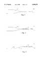
- Cross-sectional representation 90 of flash memory 74shows a portion of two flash memory cells, each including asymmetric transistor 82 formed in accordance with the method of the present invention.
- Asymmetric transistors 82are each provided with relatively thinner gate oxide region 86 and relatively thicker gate oxide region 84 beneath transistor gate 87.
- Asymmetric transistors 82are covered by insulating layer 88 and provided with common contact 78.
- Common contact 78provides an electrical connection to the drain of each asymmetric transistor 82. The use of common contact 78 in this manner saves space within a flash memory.
- Common contact 78can be formed of tungsten.
- flash memory 74can be provided with field oxide layer 80 and polycrystalline silicon conductors 76 in a conventional manner.
- Rotated cross-sectional representation 100illustrates flash memory 74 in a direction rotated ninety degrees with respect to the view of cross-sectional representation 90.
Landscapes
- Semiconductor Memories (AREA)
- Non-Volatile Memory (AREA)
Abstract
Description
Claims (18)
Priority Applications (1)
| Application Number | Priority Date | Filing Date | Title |
|---|---|---|---|
| US08/929,138US6090670A (en) | 1995-12-26 | 1997-09-05 | Highly efficient transistor for fast programming of flash memories |
Applications Claiming Priority (2)
| Application Number | Priority Date | Filing Date | Title |
|---|---|---|---|
| US08/580,459US5949117A (en) | 1995-12-26 | 1995-12-26 | Highly efficient transistor for fast programming of flash memories |
| US08/929,138US6090670A (en) | 1995-12-26 | 1997-09-05 | Highly efficient transistor for fast programming of flash memories |
Related Parent Applications (1)
| Application Number | Title | Priority Date | Filing Date |
|---|---|---|---|
| US08/580,459DivisionUS5949117A (en) | 1995-12-26 | 1995-12-26 | Highly efficient transistor for fast programming of flash memories |
Publications (1)
| Publication Number | Publication Date |
|---|---|
| US6090670Atrue US6090670A (en) | 2000-07-18 |
Family
ID=24321194
Family Applications (2)
| Application Number | Title | Priority Date | Filing Date |
|---|---|---|---|
| US08/580,459Expired - LifetimeUS5949117A (en) | 1995-12-26 | 1995-12-26 | Highly efficient transistor for fast programming of flash memories |
| US08/929,138Expired - LifetimeUS6090670A (en) | 1995-12-26 | 1997-09-05 | Highly efficient transistor for fast programming of flash memories |
Family Applications Before (1)
| Application Number | Title | Priority Date | Filing Date |
|---|---|---|---|
| US08/580,459Expired - LifetimeUS5949117A (en) | 1995-12-26 | 1995-12-26 | Highly efficient transistor for fast programming of flash memories |
Country Status (1)
| Country | Link |
|---|---|
| US (2) | US5949117A (en) |
Cited By (6)
| Publication number | Priority date | Publication date | Assignee | Title |
|---|---|---|---|---|
| US6242307B1 (en)* | 1999-08-23 | 2001-06-05 | United Microelectronics Corp. | Method of fabricating flash memory |
| US6417537B1 (en) | 2000-01-18 | 2002-07-09 | Micron Technology, Inc. | Metal oxynitride capacitor barrier layer |
| US6465828B2 (en) | 1999-07-30 | 2002-10-15 | Micron Technology, Inc. | Semiconductor container structure with diffusion barrier |
| US6476432B1 (en) | 2000-03-23 | 2002-11-05 | Micron Technology, Inc. | Structures and methods for enhancing capacitors in integrated circuits |
| US6677640B1 (en) | 2000-03-01 | 2004-01-13 | Micron Technology, Inc. | Memory cell with tight coupling |
| US20070018249A1 (en)* | 2005-07-21 | 2007-01-25 | Dongbuanam Semiconductor Inc. | Extended drain metal oxide semiconductor transistor and manufacturing method thereof |
Families Citing this family (7)
| Publication number | Priority date | Publication date | Assignee | Title |
|---|---|---|---|---|
| US5827769A (en)* | 1996-11-20 | 1998-10-27 | Intel Corporation | Method for fabricating a transistor with increased hot carrier resistance by nitridizing and annealing the sidewall oxide of the gate electrode |
| US6225661B1 (en)* | 1998-09-02 | 2001-05-01 | Advanced Micro Devices, Inc. | MOS transistor with stepped gate insulator |
| US6229184B1 (en)* | 1999-02-16 | 2001-05-08 | Advanced Micro Devices, Inc. | Semiconductor device with a modulated gate oxide thickness |
| US6291363B1 (en) | 1999-03-01 | 2001-09-18 | Micron Technology, Inc. | Surface treatment of DARC films to reduce defects in subsequent cap layers |
| US7206768B1 (en)* | 2000-08-14 | 2007-04-17 | Jpmorgan Chase Bank, N.A. | Electronic multiparty accounts receivable and accounts payable system |
| US7772062B2 (en)* | 2005-02-08 | 2010-08-10 | Taiwan Semiconductor Manufacturing Co., Ltd. | MOSFET having a channel mechanically stressed by an epitaxially grown, high k strain layer |
| US20070278557A1 (en)* | 2006-05-31 | 2007-12-06 | Texas Instruments Incorporated | Novel method to form memory cells to improve programming performance of embedded memory technology |
Citations (17)
| Publication number | Priority date | Publication date | Assignee | Title |
|---|---|---|---|---|
| US4454524A (en)* | 1978-03-06 | 1984-06-12 | Ncr Corporation | Device having implantation for controlling gate parasitic action |
| US4852062A (en)* | 1987-09-28 | 1989-07-25 | Motorola, Inc. | EPROM device using asymmetrical transistor characteristics |
| US5278087A (en)* | 1990-01-22 | 1994-01-11 | Silicon Storage Technology, Inc. | Method of making a single transistor non-volatile electrically alterable semiconductor memory device with a re-crystallized floating gate |
| US5310691A (en)* | 1990-11-06 | 1994-05-10 | Mitsubishi Denki Kabushiki Kaisha | Method of manufacturing semiconductor device including formation of alignment mark |
| US5338954A (en)* | 1991-10-31 | 1994-08-16 | Rohm Co., Ltd. | Semiconductor memory device having an insulating film and a trap film joined in a channel region |
| US5362685A (en)* | 1992-10-29 | 1994-11-08 | Advanced Micro Devices, Inc. | Method for achieving a high quality thin oxide in integrated circuit devices |
| US5376572A (en)* | 1994-05-06 | 1994-12-27 | United Microelectronics Corporation | Method of making an electrically erasable programmable memory device with improved erase and write operation |
| US5411911A (en)* | 1992-10-27 | 1995-05-02 | Sanyo Electric Co., Ltd. | Process for producing DRAM semiconductor devices |
| US5432106A (en)* | 1993-08-02 | 1995-07-11 | United Microelectronics Corporation | Manufacture of an asymmetric non-volatile memory cell |
| US5445983A (en)* | 1994-10-11 | 1995-08-29 | United Microelectronics Corporation | Method of manufacturing EEPROM memory device with a select gate |
| US5453388A (en)* | 1991-09-23 | 1995-09-26 | Integrated Silicon Solution, Inc. | Method of making an EEPROM |
| US5459091A (en)* | 1993-10-12 | 1995-10-17 | Goldstar Electron Co., Ltd. | Method for fabricating a non-volatile memory device |
| US5550078A (en)* | 1995-06-28 | 1996-08-27 | Vanguard International Semiconductor Corp. | Reduced mask DRAM process |
| US5591652A (en)* | 1993-11-08 | 1997-01-07 | Sharp Kabushiki Kaisha | Method of manufacturing flash memory with inclined channel region |
| US5897354A (en)* | 1996-12-17 | 1999-04-27 | Cypress Semiconductor Corporation | Method of forming a non-volatile memory device with ramped tunnel dielectric layer |
| US5918116A (en)* | 1994-11-30 | 1999-06-29 | Lucent Technologies Inc. | Process for forming gate oxides possessing different thicknesses on a semiconductor substrate |
| US5930631A (en)* | 1996-07-19 | 1999-07-27 | Mosel Vitelic Inc. | Method of making double-poly MONOS flash EEPROM cell |
Family Cites Families (1)
| Publication number | Priority date | Publication date | Assignee | Title |
|---|---|---|---|---|
| KR0179066B1 (en)* | 1994-11-03 | 1999-03-20 | 구자홍 | Thin film transistor and manufacturing method of the same |
- 1995
- 1995-12-26USUS08/580,459patent/US5949117A/ennot_activeExpired - Lifetime
- 1997
- 1997-09-05USUS08/929,138patent/US6090670A/ennot_activeExpired - Lifetime
Patent Citations (17)
| Publication number | Priority date | Publication date | Assignee | Title |
|---|---|---|---|---|
| US4454524A (en)* | 1978-03-06 | 1984-06-12 | Ncr Corporation | Device having implantation for controlling gate parasitic action |
| US4852062A (en)* | 1987-09-28 | 1989-07-25 | Motorola, Inc. | EPROM device using asymmetrical transistor characteristics |
| US5278087A (en)* | 1990-01-22 | 1994-01-11 | Silicon Storage Technology, Inc. | Method of making a single transistor non-volatile electrically alterable semiconductor memory device with a re-crystallized floating gate |
| US5310691A (en)* | 1990-11-06 | 1994-05-10 | Mitsubishi Denki Kabushiki Kaisha | Method of manufacturing semiconductor device including formation of alignment mark |
| US5453388A (en)* | 1991-09-23 | 1995-09-26 | Integrated Silicon Solution, Inc. | Method of making an EEPROM |
| US5338954A (en)* | 1991-10-31 | 1994-08-16 | Rohm Co., Ltd. | Semiconductor memory device having an insulating film and a trap film joined in a channel region |
| US5411911A (en)* | 1992-10-27 | 1995-05-02 | Sanyo Electric Co., Ltd. | Process for producing DRAM semiconductor devices |
| US5362685A (en)* | 1992-10-29 | 1994-11-08 | Advanced Micro Devices, Inc. | Method for achieving a high quality thin oxide in integrated circuit devices |
| US5432106A (en)* | 1993-08-02 | 1995-07-11 | United Microelectronics Corporation | Manufacture of an asymmetric non-volatile memory cell |
| US5459091A (en)* | 1993-10-12 | 1995-10-17 | Goldstar Electron Co., Ltd. | Method for fabricating a non-volatile memory device |
| US5591652A (en)* | 1993-11-08 | 1997-01-07 | Sharp Kabushiki Kaisha | Method of manufacturing flash memory with inclined channel region |
| US5376572A (en)* | 1994-05-06 | 1994-12-27 | United Microelectronics Corporation | Method of making an electrically erasable programmable memory device with improved erase and write operation |
| US5445983A (en)* | 1994-10-11 | 1995-08-29 | United Microelectronics Corporation | Method of manufacturing EEPROM memory device with a select gate |
| US5918116A (en)* | 1994-11-30 | 1999-06-29 | Lucent Technologies Inc. | Process for forming gate oxides possessing different thicknesses on a semiconductor substrate |
| US5550078A (en)* | 1995-06-28 | 1996-08-27 | Vanguard International Semiconductor Corp. | Reduced mask DRAM process |
| US5930631A (en)* | 1996-07-19 | 1999-07-27 | Mosel Vitelic Inc. | Method of making double-poly MONOS flash EEPROM cell |
| US5897354A (en)* | 1996-12-17 | 1999-04-27 | Cypress Semiconductor Corporation | Method of forming a non-volatile memory device with ramped tunnel dielectric layer |
Non-Patent Citations (4)
| Title |
|---|
| Robinson, "Endurance Brightens the Future of Flash", Electronic Component News, Nov. 1988, Reprinted in nonvolatile Semiconductor Memories Technologies, Design and Applications, IEEE Press pp. 167-168. |
| Robinson, Endurance Brightens the Future of Flash , Electronic Component News, Nov. 1988, Reprinted in nonvolatile Semiconductor Memories Technologies, Design and Applications, IEEE Press pp. 167 168.* |
| S. Wolf and R.N. Tauber, Silicon Processing for the VLSI Era, vol. 1, Lattice Press, pp. 57 58 and 210 211, 1986.* |
| S. Wolf and R.N. Tauber, Silicon Processing for the VLSI Era, vol. 1, Lattice Press, pp. 57-58 and 210-211, 1986. |
Cited By (19)
| Publication number | Priority date | Publication date | Assignee | Title |
|---|---|---|---|---|
| US6780706B2 (en) | 1999-07-30 | 2004-08-24 | Micron Technology, Inc. | Semiconductor container structure with diffusion barrier |
| US6465828B2 (en) | 1999-07-30 | 2002-10-15 | Micron Technology, Inc. | Semiconductor container structure with diffusion barrier |
| US6242307B1 (en)* | 1999-08-23 | 2001-06-05 | United Microelectronics Corp. | Method of fabricating flash memory |
| US6631069B2 (en) | 2000-01-18 | 2003-10-07 | Micron Technology, Inc. | Metal oxynitride capacitor barrier layer |
| US20040085802A1 (en)* | 2000-01-18 | 2004-05-06 | Micron Technology, Inc. | Metal oxynitride capacitor barrier layer |
| US6664584B2 (en) | 2000-01-18 | 2003-12-16 | Micron Technology, Inc. | Metal oxynitride capacitor barrier layer |
| US6664583B2 (en) | 2000-01-18 | 2003-12-16 | Micron Technology, Inc. | Metal oxynitride capacitor barrier layer |
| US6670256B2 (en) | 2000-01-18 | 2003-12-30 | Micron Technology, Inc. | Metal oxynitride capacitor barrier layer |
| US7015527B2 (en) | 2000-01-18 | 2006-03-21 | Micron Technology, Inc. | Metal oxynitride capacitor barrier layer |
| US7002202B2 (en) | 2000-01-18 | 2006-02-21 | Micron Technology, Inc. | Metal oxynitride capacitor barrier layer |
| US6417537B1 (en) | 2000-01-18 | 2002-07-09 | Micron Technology, Inc. | Metal oxynitride capacitor barrier layer |
| US20040102002A1 (en)* | 2000-03-01 | 2004-05-27 | Micron Technology, Inc. | Memory cell with tight coupling |
| US6677640B1 (en) | 2000-03-01 | 2004-01-13 | Micron Technology, Inc. | Memory cell with tight coupling |
| US7241661B2 (en) | 2000-03-01 | 2007-07-10 | Micron Technology, Inc. | Method of forming a coupling dielectric Ta2O5 in a memory device |
| US6476432B1 (en) | 2000-03-23 | 2002-11-05 | Micron Technology, Inc. | Structures and methods for enhancing capacitors in integrated circuits |
| US6861330B2 (en) | 2000-03-23 | 2005-03-01 | Micron Technology Inc. | Structures and methods for enhancing capacitors in integrated circuits |
| US6696716B2 (en) | 2000-03-23 | 2004-02-24 | Micron Technology, Inc. | Structures and methods for enhancing capacitors in integrated ciruits |
| US20070018249A1 (en)* | 2005-07-21 | 2007-01-25 | Dongbuanam Semiconductor Inc. | Extended drain metal oxide semiconductor transistor and manufacturing method thereof |
| US7385261B2 (en)* | 2005-07-21 | 2008-06-10 | Dongbu Electronics Co., Ltd. | Extended drain metal oxide semiconductor transistor and manufacturing method thereof |
Also Published As
| Publication number | Publication date |
|---|---|
| US5949117A (en) | 1999-09-07 |
Similar Documents
| Publication | Publication Date | Title |
|---|---|---|
| US5614747A (en) | Method for manufacturing a flash EEPROM cell | |
| US5460988A (en) | Process for high density flash EPROM cell | |
| US6445030B1 (en) | Flash memory erase speed by fluorine implant or fluorination | |
| US5459091A (en) | Method for fabricating a non-volatile memory device | |
| US6188103B1 (en) | Method of forming sharp beak of poly by nitrogen implant to improve erase speed for split-gate flash | |
| USRE35810E (en) | Plug-based floating gate memory | |
| KR100979661B1 (en) | Dielectric storage memory cell (MOONOS) having a high dielectric constant uppermost dielectric and its method | |
| US5930631A (en) | Method of making double-poly MONOS flash EEPROM cell | |
| US6576511B2 (en) | Method for forming nitride read only memory | |
| US6252276B1 (en) | Non-volatile semiconductor memory device including assymetrically nitrogen doped gate oxide | |
| US6090670A (en) | Highly efficient transistor for fast programming of flash memories | |
| US5703388A (en) | Double-poly monos flash EEPROM cell | |
| US6001713A (en) | Methods for forming nitrogen-rich regions in a floating gate and interpoly dielectric layer in a non-volatile semiconductor memory device | |
| US6069042A (en) | Multi-layer spacer technology for flash EEPROM | |
| US6180977B1 (en) | Self-aligned edge implanted cell to reduce leakage current and improve program speed in split-gate flash | |
| US6667509B1 (en) | Method of forming sharp beak of poly by oxygen/fluorine implant to improve erase speed for split-gate flash | |
| US5422292A (en) | Process for fabricating split gate flash EEPROM memory | |
| US5643812A (en) | Method of making EEPROM flash memory cell with erase gate | |
| US5445982A (en) | Method of fabricating nonvolatile semiconductor memory device | |
| US7186615B2 (en) | Method of forming a floating gate for a split-gate flash memory device | |
| US6429472B2 (en) | Split gate type flash memory | |
| US7118969B2 (en) | Method of manufacturing a floating gate and method of manufacturing a non-volatile semiconductor memory device comprising the same | |
| JP4969748B2 (en) | Nonvolatile semiconductor memory device and method of manufacturing nonvolatile memory cell | |
| US5726070A (en) | Silicon-rich tunnel oxide formed by oxygen implantation for flash EEPROM | |
| US6989319B1 (en) | Methods for forming nitrogen-rich regions in non-volatile semiconductor memory devices |
Legal Events
| Date | Code | Title | Description |
|---|---|---|---|
| STCF | Information on status: patent grant | Free format text:PATENTED CASE | |
| FPAY | Fee payment | Year of fee payment:4 | |
| FPAY | Fee payment | Year of fee payment:8 | |
| FPAY | Fee payment | Year of fee payment:12 | |
| AS | Assignment | Owner name:U.S. BANK NATIONAL ASSOCIATION, AS COLLATERAL AGENT, CALIFORNIA Free format text:SECURITY INTEREST;ASSIGNOR:MICRON TECHNOLOGY, INC.;REEL/FRAME:038669/0001 Effective date:20160426 Owner name:U.S. BANK NATIONAL ASSOCIATION, AS COLLATERAL AGEN Free format text:SECURITY INTEREST;ASSIGNOR:MICRON TECHNOLOGY, INC.;REEL/FRAME:038669/0001 Effective date:20160426 | |
| AS | Assignment | Owner name:MORGAN STANLEY SENIOR FUNDING, INC., AS COLLATERAL AGENT, MARYLAND Free format text:PATENT SECURITY AGREEMENT;ASSIGNOR:MICRON TECHNOLOGY, INC.;REEL/FRAME:038954/0001 Effective date:20160426 Owner name:MORGAN STANLEY SENIOR FUNDING, INC., AS COLLATERAL Free format text:PATENT SECURITY AGREEMENT;ASSIGNOR:MICRON TECHNOLOGY, INC.;REEL/FRAME:038954/0001 Effective date:20160426 | |
| AS | Assignment | Owner name:U.S. BANK NATIONAL ASSOCIATION, AS COLLATERAL AGENT, CALIFORNIA Free format text:CORRECTIVE ASSIGNMENT TO CORRECT THE REPLACE ERRONEOUSLY FILED PATENT #7358718 WITH THE CORRECT PATENT #7358178 PREVIOUSLY RECORDED ON REEL 038669 FRAME 0001. ASSIGNOR(S) HEREBY CONFIRMS THE SECURITY INTEREST;ASSIGNOR:MICRON TECHNOLOGY, INC.;REEL/FRAME:043079/0001 Effective date:20160426 Owner name:U.S. BANK NATIONAL ASSOCIATION, AS COLLATERAL AGEN Free format text:CORRECTIVE ASSIGNMENT TO CORRECT THE REPLACE ERRONEOUSLY FILED PATENT #7358718 WITH THE CORRECT PATENT #7358178 PREVIOUSLY RECORDED ON REEL 038669 FRAME 0001. ASSIGNOR(S) HEREBY CONFIRMS THE SECURITY INTEREST;ASSIGNOR:MICRON TECHNOLOGY, INC.;REEL/FRAME:043079/0001 Effective date:20160426 | |
| AS | Assignment | Owner name:MICRON TECHNOLOGY, INC., IDAHO Free format text:RELEASE BY SECURED PARTY;ASSIGNOR:U.S. BANK NATIONAL ASSOCIATION, AS COLLATERAL AGENT;REEL/FRAME:047243/0001 Effective date:20180629 | |
| AS | Assignment | Owner name:MICRON TECHNOLOGY, INC., IDAHO Free format text:RELEASE BY SECURED PARTY;ASSIGNOR:MORGAN STANLEY SENIOR FUNDING, INC., AS COLLATERAL AGENT;REEL/FRAME:050937/0001 Effective date:20190731 |