US6088800A - Encryption processor with shared memory interconnect - Google Patents
Encryption processor with shared memory interconnectDownload PDFInfo
- Publication number
- US6088800A US6088800AUS09/032,029US3202998AUS6088800AUS 6088800 AUS6088800 AUS 6088800AUS 3202998 AUS3202998 AUS 3202998AUS 6088800 AUS6088800 AUS 6088800A
- Authority
- US
- United States
- Prior art keywords
- data
- processing
- adder
- processing elements
- segments
- Prior art date
- Legal status (The legal status is an assumption and is not a legal conclusion. Google has not performed a legal analysis and makes no representation as to the accuracy of the status listed.)
- Ceased
Links
Images


Classifications
- H—ELECTRICITY
- H04—ELECTRIC COMMUNICATION TECHNIQUE
- H04L—TRANSMISSION OF DIGITAL INFORMATION, e.g. TELEGRAPHIC COMMUNICATION
- H04L9/00—Cryptographic mechanisms or cryptographic arrangements for secret or secure communications; Network security protocols
- G—PHYSICS
- G06—COMPUTING OR CALCULATING; COUNTING
- G06F—ELECTRIC DIGITAL DATA PROCESSING
- G06F7/00—Methods or arrangements for processing data by operating upon the order or content of the data handled
- G06F7/38—Methods or arrangements for performing computations using exclusively denominational number representation, e.g. using binary, ternary, decimal representation
- G06F7/48—Methods or arrangements for performing computations using exclusively denominational number representation, e.g. using binary, ternary, decimal representation using non-contact-making devices, e.g. tube, solid state device; using unspecified devices
- G06F7/52—Multiplying; Dividing
- G06F7/523—Multiplying only
- G06F7/53—Multiplying only in parallel-parallel fashion, i.e. both operands being entered in parallel
- G06F7/5324—Multiplying only in parallel-parallel fashion, i.e. both operands being entered in parallel partitioned, i.e. using repetitively a smaller parallel parallel multiplier or using an array of such smaller multipliers
- G—PHYSICS
- G06—COMPUTING OR CALCULATING; COUNTING
- G06F—ELECTRIC DIGITAL DATA PROCESSING
- G06F7/00—Methods or arrangements for processing data by operating upon the order or content of the data handled
- G06F7/38—Methods or arrangements for performing computations using exclusively denominational number representation, e.g. using binary, ternary, decimal representation
- G06F7/48—Methods or arrangements for performing computations using exclusively denominational number representation, e.g. using binary, ternary, decimal representation using non-contact-making devices, e.g. tube, solid state device; using unspecified devices
- G06F7/50—Adding; Subtracting
- G06F7/505—Adding; Subtracting in bit-parallel fashion, i.e. having a different digit-handling circuit for each denomination
- G06F7/5052—Adding; Subtracting in bit-parallel fashion, i.e. having a different digit-handling circuit for each denomination using carry completion detection, either over all stages or at sample stages only
- G—PHYSICS
- G06—COMPUTING OR CALCULATING; COUNTING
- G06F—ELECTRIC DIGITAL DATA PROCESSING
- G06F7/00—Methods or arrangements for processing data by operating upon the order or content of the data handled
- G06F7/60—Methods or arrangements for performing computations using a digital non-denominational number representation, i.e. number representation without radix; Computing devices using combinations of denominational and non-denominational quantity representations, e.g. using difunction pulse trains, STEELE computers, phase computers
- G06F7/72—Methods or arrangements for performing computations using a digital non-denominational number representation, i.e. number representation without radix; Computing devices using combinations of denominational and non-denominational quantity representations, e.g. using difunction pulse trains, STEELE computers, phase computers using residue arithmetic
- G06F7/722—Modular multiplication
- H—ELECTRICITY
- H04—ELECTRIC COMMUNICATION TECHNIQUE
- H04L—TRANSMISSION OF DIGITAL INFORMATION, e.g. TELEGRAPHIC COMMUNICATION
- H04L9/00—Cryptographic mechanisms or cryptographic arrangements for secret or secure communications; Network security protocols
- H04L9/14—Cryptographic mechanisms or cryptographic arrangements for secret or secure communications; Network security protocols using a plurality of keys or algorithms
- G—PHYSICS
- G06—COMPUTING OR CALCULATING; COUNTING
- G06F—ELECTRIC DIGITAL DATA PROCESSING
- G06F2207/00—Indexing scheme relating to methods or arrangements for processing data by operating upon the order or content of the data handled
- G06F2207/38—Indexing scheme relating to groups G06F7/38 - G06F7/575
- G06F2207/3804—Details
- G06F2207/3808—Details concerning the type of numbers or the way they are handled
- G06F2207/3812—Devices capable of handling different types of numbers
- G06F2207/382—Reconfigurable for different fixed word lengths
- G—PHYSICS
- G06—COMPUTING OR CALCULATING; COUNTING
- G06F—ELECTRIC DIGITAL DATA PROCESSING
- G06F2207/00—Indexing scheme relating to methods or arrangements for processing data by operating upon the order or content of the data handled
- G06F2207/38—Indexing scheme relating to groups G06F7/38 - G06F7/575
- G06F2207/3804—Details
- G06F2207/3808—Details concerning the type of numbers or the way they are handled
- G06F2207/3828—Multigauge devices, i.e. capable of handling packed numbers without unpacking them
- G—PHYSICS
- G06—COMPUTING OR CALCULATING; COUNTING
- G06F—ELECTRIC DIGITAL DATA PROCESSING
- G06F7/00—Methods or arrangements for processing data by operating upon the order or content of the data handled
- G06F7/38—Methods or arrangements for performing computations using exclusively denominational number representation, e.g. using binary, ternary, decimal representation
- G06F7/48—Methods or arrangements for performing computations using exclusively denominational number representation, e.g. using binary, ternary, decimal representation using non-contact-making devices, e.g. tube, solid state device; using unspecified devices
- G06F7/499—Denomination or exception handling, e.g. rounding or overflow
- G06F7/49931—Modulo N reduction of final result
- H—ELECTRICITY
- H04—ELECTRIC COMMUNICATION TECHNIQUE
- H04L—TRANSMISSION OF DIGITAL INFORMATION, e.g. TELEGRAPHIC COMMUNICATION
- H04L2209/00—Additional information or applications relating to cryptographic mechanisms or cryptographic arrangements for secret or secure communication H04L9/00
- H04L2209/12—Details relating to cryptographic hardware or logic circuitry
- H04L2209/125—Parallelization or pipelining, e.g. for accelerating processing of cryptographic operations
Definitions
- Privacyis accomplished through encryption/decryption.
- encryption/decryptionis performed based on algorithms which are intended to allow data transfer over an open channel between parties while maintaining the privacy of the message contents. This is accomplished by encrypting the data using an encryption key by the sender and decrypting it using a decryption key by the receiver (sometimes, the encryption and decryption keys are the same).
- Encryption algorithmscan be classified into public-key and secret key algorithms. In secret-key algorithms, both keys are secret whereas in public-key algorithms, one of the keys is known to the general public.
- Block ciphersare representative of the secret-key cryptosystems in use today. Usually, for block ciphers, the encryption key is the same as the decryption key. A block cipher takes a block of data, typically 32-128 bits, as input and produces the same number of bits as output. The encryption and decryption are performed using a key, anywhere from 56-128 bits in length. The encryption algorithm is designed such that it is very difficult to decrypt a message without knowing the key.
- a public key cryptosystemsuch as the Rivest, Shamir, Adelman (RSA) cryptosystem described in U.S. Pat. No. 5,144,667 issued to Pogue and Rivest uses two keys, only one of which is made public. Once someone publishes a key, anyone may send that person a secret message using that key. However, decryption of the message can only be accomplished by use of the secret key.
- the advantage of such public-key encryptionis secret keys do not need to be distributed to all parties of a conversation beforehand. In contrast, if only secret-key encryption were used, multiple secret keys would have to be generated, one for each party intended to receive the message, and each secret key would have to be privately communicated. Attempting to communicate the secret key privately results in the same problem as in sending the message itself using only secret-key encryption; this is called the key distribution problem.
- Key exchangeis another application of public-key techniques.
- a key exchange protocoltwo parties can agree on a secret key even if their conversation is intercepted by a third party.
- the Diffie-Hellman exponential key exchangedescribed in U.S. Pat. No. 4,200,770, is an example of such a protocol.
- a Pentium®can perform a 32 ⁇ 32-bit multiply in 10 clock cycles.
- a 2048-bit numbercan be represented in 64 32-bit words.
- a 2048 ⁇ 2048-bit multiplyrequires 64 ⁇ 64 separate 32 ⁇ 32-bit multiplications, which takes 40960 clocks on the Pentium.
- An exponentiation with a 2048-bit exponentrequires up to 4096 multiplications if done in the normal way, which requires about 167 million clock cycles.
- public-key algorithmsare so computationally intensive, they are typically not used to encrypt entire messages. Instead, private-key cryptosystems are used for message transfer.
- the private key used to encrypt the messagecalled the session key, is chosen at random and encrypted using a public key.
- the encrypted session key, as well as the encrypted message,are then sent to the other party.
- the other partyuses its secret key to decrypt the session key, at which point the message may be decrypted using the session key.
- a different session keyis used for each communication, so that if one session key is ever broken, only the one message encrypted with it may be read.
- This public-key/private-key methodcan also be used to protect continuous communications, such as interactive terminal sessions that never terminate in normal operation. In this case, the session key is periodically changed (e.g. once an hour) by repeating the public-key generation technique. Again, frequent changing of the session key limits the amount of data compromised if the encryption is broken.
- Network-level encryption devicesallowing access to corporate networks using a software-based solution are experiencing widespread usage.
- Productssuch as Raptor Eagle Remote and others perform encryption entirely in software.
- the softwarelimits the encryptor's throughput. Session key generation using public-key techniques may take several minutes. For this reason, session keys are not re-generated as often as some people would like.
- softwaredoes have the advantage that the encryption algorithms are easily changed in response to advances in the field.
- the Sentinelalso makes use of a Motorola DSP56000 processor to perform the public-key operations.
- the single-cycle multiplication ability of the DSPmade this approach significantly faster than implementing the public-key algorithms on regular CISC microprocessors.
- a preferred high-performance programmable network encryption deviceintegrated into a single chip, is a parallel-pipelined processor system whose instruction set is optimized for common encryption algorithms.
- the present inventionrealizes the advantages of both hardware and software approaches. Since the processor is a programmable processor, any encryption algorithm may be implemented, contrary to a hardware implemented encryption processor which is dedicated to executing only one algorithm. However, the processor's architecture permits parallel computations of a nature useful for encryption, so its performance more closely approximates that of a dedicated hardware device.
- an electronic encryption devicecomprises an array of processing elements.
- Each processing elementcomprises an instruction memory for storing a round of an encryption algorithm, the round comprising a sequence of instructions.
- the processing elementalso includes a processor for implementing the round from the instruction memory and data storage for storing encryption data operands and encrypted data resulting from implementing the round.
- Each processing element of the arrayimplements one of the rounds and transfers results to successive processing elements such that the array of processing elements implements successive rounds of the encryption algorithm in a processing element pipeline.
- the data storagehas a portion thereof which is shared between adjacent processing elements of the linear array for transfer of data between adjacent processing elements of the linear array.
- the shared data storageis preferably comprised of dual port memories but may also comprise shared registers.
- the preferred processing elementcomprises a control unit and an ALU.
- the control unit, ALU, instruction memory and data storage, including local data memory and shared data memory,are connected to a local processing element bus.
- the local busis segmented by a switch into a local instruction bus segment, connecting the instruction memory and the control unit, and a local data bus segment connecting the ALU, local data memory and shared data memory.
- the switchpermits either independent simultaneous operation on the two local bus segments or a communication between the two bus segments.
- Each processing elementfurther comprises a multiplier for performing multiplication operations within the processing element.
- the preferred encryption devicefurther comprises a global random access memory and a global bus through which data is transferred between the global random access memory and the processing element data storage.
- a central processoris coupled to the global bus for processing data words which are wider than data words processed by the processing elements.
- the multipliers of the plural processing elementsmay be adapted for concatenation as segments of a wider multiplier used by the central processor.
- each multipliercomprises partial product adders having input selection circuitry for selecting a first set of inputs when operating as an individual multiplier and a second set of inputs, including inputs from adjacent processing elements, when concatenated.
- the central processorcomprises a novel adder.
- each of plural adder segmentshas a carry output and a sum output and each of the adder segments processes a segment of each of two operands.
- Selectorsselect the carry outputs as carry inputs to successive adder segments for successive clock cycles so long as any carry results in an adder cycle.
- Selectorsalso select each sum output as an operand input to the same adder segment. Accordingly, so long as any carry results in an adder cycle, the sum output of an adder is fed back to its input, and the adder segment receives a carry input generated as a carry output from a preceding segment in a preceding cycle.
- each processing elementperforms a modular adjust operation to compute M mod N without using a divide circuit.
- Each processing elementalso performs a modulo add/subtract operation to compute A ⁇ B mod N. Further, each processing element performs a modulo multiply operation to compute A ⁇ B mod N.
- FIGS. 1A and 1Bare block diagrams of potential applications of the present invention.
- FIG. 2is a block diagram of an encryption chip embodying the present invention.
- FIG. 3is a block diagram of a processing element in the encryption chip of FIG. 2.
- FIG. 4illustrates a preferred chip layout of the circuitry of FIGS. 2 and 3.
- FIG. 5illustrates the processing element of FIG. 3 redrawn to correspond to the layout of FIG. 4 and to illustrate the PE local bus and global bus connections.
- FIG. 6illustrates an adder circuit used in the PK ALU of FIG. 2.
- FIG. 7illustrates a full adder symbol used in a multiplier of the PK ALU.
- FIG. 8illustrates processing in the first stage of a 4 ⁇ 4 multiplier using full adders.
- FIG. 9illustrates three stages of the 4 ⁇ 4 multiplier.
- FIG. 10illustrates the adders of a wide multiplier with the adders of the 4 ⁇ 4 multiplier overlaid thereon.
- FIG. 11is a block diagram of a 4 ⁇ 4 multiplier adapted to be concatenated with like multipliers in a wide word length multiplier of FIG. 10.
- FIG. 12illustrates a conventional implementation of an 8-bit adder using full adders.
- FIG. 13is a conventional implementation of a carry lookahead adder.
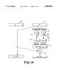
- FIG. 14is a block diagram illustration of a DES encryption round.
- FIGS. 15A-Dare functional diagrams illustrating modular add, subtract, adjust and combination of all three operations according to embodiments of the present invention.
- the encryption chip of the present inventionmay be programmed to perform common data encryption and decryption algorithms on one or more data streams in any application.
- the principal purpose of the encryption chipis to perform high speed data encryption using algorithms that are expected to be in use on the Internet, at data rates of 100-2000 Mbps.
- Example applicationsare illustrated in FIGS. 1A and 12.
- data from a source 22is encrypted in an encryption chip 24 before the data is passed into a public network 26.
- the datais then decrypted in encryption chip 28 before being forwarded to a destination 30.
- the source and the destinationare themselves networks such as local area networks. In that case, the encryption chips provide a secure path between the local area networks and the public network 26.
- DESThree main secret-key block encryption algorithms are in common use today: DES, RC5 and IDEA.
- the first two algorithmsare standard Internet Protocol SECurity IPSEC standard algorithms.
- IDEAis the algorithm used by PGP, a popular email encryption program.
- block algorithmsconsist of a number of rounds; each round is a sequence of operations in an encryption algorithm. Anywhere from 8-32 rounds are required to completely implement an encryption algorithm.
- the operations performed by each roundare often the same, although they need not be.
- each roundis implemented with a few machine instructions.
- each roundis implemented with dedicated circuitry. The hardware is typically pipelined, with each round being implemented in its own pipeline stage.
- FIG. 2illustrates an integrated chip solution, henceforth referred to as the encryption chip, according to an embodiment of the present invention.
- the encryption chipimplies the chip can perform encryption, it should be noted that the chip is also designed to perform decryption and message digest functions as well.
- the input stageconverts the serial data stream to block-aligned data suitable for processing as an input to an encryption/decryption pipeline.
- the size of the input blocksis programmable.
- the pipelineis made up of a plurality of processing elements 37 arranged in a linear array, each containing an instruction memory, a register file, an ALU, local and shared data memory, and control circuitry. Each of the processing elements is designed to process 32-bit wide data words.
- the encrypted datais taken from the last processing element in the pipeline into an output stage 42, which converts the block data back into a serial stream format and forwards the data over the network or to a local destination.
- Datacan be transferred among non-adjacent processing elements and/or other elements within the encryption ship via a global data bus 38.
- I/O communication logic 54which allows communication with a host CPU (not shown). Host CPU communication is required to program the encryption chip prior to use.
- Global random access memory (RAM) 44is also connected to the global data bus 38, allowing global communication among the processing elements.
- a control CPU 52synchronizes the operations of the encryption pipeline processors. This CPU may be implemented using any available embedded CPU core such as MIPS, ARM or ARC.
- a public-key (PK) core processor 46is connected to the control CPU 52.
- the PK coreincludes a register file 48 consisting of 8-16 512-bit wide registers as well as a PK ALU 50.
- the PK core processorcan make data transfers to and from the global RAM 44 over a 512-bit bus in one system clock cycle. 512-bit operands are processed in the ALU 50, typically in 2-32 clock cycles.
- the PK core ALU 50is a coprocessor controlled by the control CPU 52, performing only arithmetic and logic operations along with loads and stores. Other instructions necessary for implementing PK algorithms can be executed within the control CPU 52.
- the encryption chipimplements the code for each round of a secret key algorithm in a separate processing element of the pipeline. Once computed upon, data from one PE is transferred to the next PE where the next round is implemented. The first PE is then free to process an encryption round for the next block of data coming in. The pipeline process continues for the remaining PE's. The time required to encrypt a block using this architecture is therefore equal to the time required to encrypt one round.
- the basic application of a block algorithmtransforms a block of plaintext (unencrypted information) into a similar-sized block of ciphertext (encrypted information) and vice-versa.
- This operating modeis known as electronic codebook (ECB) mode. Due to its many inherent security weaknesses, methods of introducing feedback into the encryption by cycling some of the basic output back into the input are commonly used.
- the encryption chipuses the global data bus 38 to perform cipher feedback (CFB).
- CFBcipher feedback
- ECB modea new block of data can be encrypted once per pipeline cycle, which can be 10-100 instructions.
- CFB modeeach datum must pass through the pipeline multiple times. This mode substantially reduces throughput on a single channel.
- peak performancecan be achieved by encrypting multiple data channels, interleaved in the pipeline.
- FIG. 3A block diagram of one individual processing element PE according to an embodiment of the present invention is shown in FIG. 3.
- the processing element 37consists of an ALU 56 operating on 32-bit words from a register file 58 made up of 8-16 32-bit registers.
- the register file 58 and ALU 56are controlled by a control unit 60 which decodes instructions from a processing element instruction memory 62.
- Each processing element instruction memorystores at least one round of an encryption algorithm, where a round is defined as a sequence of instructions in an encryption algorithm.
- the PE data memory space accessible by each processing elementis divided into four areas: a local PE memory 64 (in FIG. 3, designated as PE n local memory), a shared memory 66 (in FIG.
- PE n ,n-1 shared memory shared between the n-th and n-1-th processing elementshared memory shared between the n-th and n-1-th processing element
- a second shared memory 68in FIG. 3, designated as PE n+1 ,n shared memory shared between the n+1-st and n-th processing element
- the global memory 44as described with reference to FIG. 2, which is accessible to all PEs. All of these memories are mapped into the address space of a processing element, say the n-th processing element. No special instructions are required to access any type of memory; all memories are accessible by all memory access instructions.
- the memories 66 and 68 of a processing elementare dual port SRAMs and are shared with the PE of the previous and next pipe stage, respectively. Note that a PE's next-neighbor memory is the same as the next PE's previous-neighbor memory.
- the global memory 44is connected to the global communication bus. Only one processing element is allowed to access the global memory 44 at any one time. This memory is used to pass data between non-adjacent processing elements, for example, during feedback encryption algorithms and can serve as supplemental storage for individual processing elements.
- the PE instruction memory 62has an instruction set resembling that of a modern RISC processor integer unit.
- the instruction setis more or less orthogonal in that any register can be used as an operand to any instruction. No floating-point or memory management support need be provided, since neither are useful in encryption.
- the instruction setcontains the following useful enhancements: a modular addition/subtraction instruction, a modular multiplication instruction and a modulo adjust instruction.
- FIGS. 15A through 15Dillustrate the combination of the modular add, subtract and adjust into one 3-in-1 modulo arithmetic unit.
- FIG. 15Aillustrates the modular add operation. If the two numbers to be added, A and B, are both less than N, then their sum from adder 120 can be reduced modulo N by subtracting N in subtractor 122, and then selecting through the multiplexer 124 either the output of the subtractor or the original number, depending on the sign of the difference. Similarly, in the case of a modular subtract operation as shown in FIG. 15B, if the two numbers A and B are less than N, then their difference modulo N can be computed by adding N in adder 126 if the difference from subtractor 128 is negative or by selecting the difference through multiplexor 130 if the difference is positive. Note that both the modulo add and modulo subtract do not require division.
- the reduction modulo Ncan be encoded as a separate instruction, which is called the "modulo adjust" instruction.
- the modulo adjust instructionillustrated in FIG. 15C, computes M mod N, given that M is either a sum or a difference of A and B, both already reduced to mod N. If M is negative, the logic 132 causes adder/subtractor 134 to add N to M to produce the result through multiplexor 136. If M is positive, then logic 132 causes subtraction of N, and returns the difference if it is positive or M if the difference is negative. This instruction may be used in conjunction with sum and difference instructions to render the modular addition/subtraction instruction unnecessary.
- the 3-in-1 arithmetic unitcombines the modulo add, modulo subtract and modulo adjust into a single unit which is implemented within each processing element.
- adder/subtractor 138serves the function of either of devices 120 and 128, and adder/subtractor 140 serves the function of any of devices 122, 126 and 134.
- Multiplexor 142corresponds to devices 124, 130 and 136.
- Mis applied to the A input and the B input is set at zero.
- This combined unitis most efficient in area at the cost of speed.
- This combined unitis also useful in implementing Montgomery's method for modular multiplication without trial division, "Modular Multiplication Without Trial Division," by Peter L. Montgomery, Mathematics of Computation, Vol. 44, No. 170, April 1985, pages 519-521.
- the modular multiplication instructioncomputes A*B mod N.
- the multiplier used for this instructionwill be described in more detail below.
- the encryption chipprovides a full modular multiply instruction, for reasons which will become clear below.
- Table 1gives a representative sample of the instruction set of the PEs to be used in subsequent examples. Other conventional RISC instructions may also be implemented.
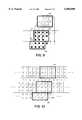
- FIG. 4A general layout of the encryption chip is illustrated in FIG. 4, assuming 16 processing elements and a 512-bit wide public key PK core unit.
- the PK core word width of 512 bitswas chosen due to its layout convenience.
- a width of 1024 bits for example,would require more silicon area but would also double performance.
- the individual elementscan be compared to the elements of FIGS. 2 and 3. Sixteen of the processing elements are linearly arranged in a column in the large region of the layout to the lower left, one being shown in detail.
- the shared multiplier element 70is shown associated with the illustrated processing element. As previously described, a 32 ⁇ 32 multiplier segment 70 is associated with each processing element for performing 32-bit multiplications within the respective processing elements. Alternatively, the multiplier elements 70 can be concatenated to serve as a wide 512 ⁇ 32 bit multiplier for the public-key ALU 50.
- the public-key PK ALU 50is located to the right of the secret-key SK elements, made up of the processing elements as described above. Next to the PK ALU is the PK register file 48.
- the PK ALU 50 and the PK register file 48make up the PK processing core, identified in FIG. 2 as 46.
- To the right of the PK coreis located the global memory (RAM) 44.
- the control CPU 52Along the top of the chip are the control CPU 52, the communication logic 54 and the input and output processing blocks 40 and 42.
- the global data bus 38links the SK elements, the PK core 46, the global RAM 44, the communication logic 54 and the control CPU 52.
- FIG. 5The layout of a typical processing element with the local bus connections is shown in FIG. 5. All components of a processing element may communicate via a local processing element data bus 72, which handles all the memory--register transfers. Note that the next-neighbor shared PE memory 68 is laid out in line with the other elements of the illustrated processing element, whereas, the previous-neighbor shared PE memory 66 is laid out in line with the elements of the previous-neighbor processing element. For programming and testing purposes, all PE memories are accessible from the global bus 38.
- a switch 74normally disconnects the local bus 72 from the global bus 38 but may be selectively closed to enable data transfer between the local RAM 64 and the global RAM 44.
- Another switch 76allows the local bus 72 to be segmented into independent segments such that the control unit 60 can read instructions from the RAM 62 simultaneously with transfer of data on the bus 72. As such, operations within the processing element may be pipelined with one instruction being processed in the control unit while a prior instruction is executed in the PE ALU 56. During execution of encryption code, switches 74 and 76 are normally open, so that instruction fetches from the instruction RAM may proceed concurrently with data fetches from the data memories and register file.
- Efficient public-key encryptionrequires efficient modular exponentiation, provided by the public-key co-processor.
- This unitcomprises the following items:
- PK register file 48consisting of 16 512-bit wide registers
- PK 512 ⁇ 32-bit multiplier 70made up of concatenated SK multiplier elements (this unit can perform a 512 ⁇ 512 multiply in only 32 clock cycles)
- PK 512-bit adder ALU 50which can perform addition in 2-16 cycles, typically no more than 2
- global memory 44organized for 512-bit parallel access from the PK coprocessor for loading and storing 512-bit words in a single clock cycle
- the PK core processoraccelerates modular multiplication by performing it using 512-bit words.
- a 512 ⁇ 512 multiply operation using the PK unit of the inventionwould be implemented by performing 16 512 ⁇ 32 multiplies using the concatenated multiplier elements of the 16 processing elements described below. Assuming each multiply requires 2 clock cycles and 16 such multiplies are required, a 512 ⁇ 512 multiply would require 32 clock cycles and a 2048 ⁇ 2048 multiply would require only 512 clock cycles. The full modular exponentiation operation, requiring 4096 multiplies, would take a total of 2 million clock cycles. This represents an 80 fold improvement to the Pentium example discussed earlier. The performance improvement of PK algorithms is expected to be similar. This represents a significant performance gain compared to the prior art, and will enable more frequent changing of session keys, thereby increasing security.
- Addersare not shared between the public key PK and secret key SK units. Rather, since addition and logic operations are common for both PK and SK, each unit has its own adder, so that operations may proceed concurrently.
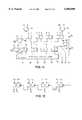
- the 512-bit adder in the ALU 50is formed of 16 32-bit adders as illustrated in FIG. 6.
- the AND-gate 78 and multiplexer 80initially apply two 32-bit operand segments to each of the 32-bit adders A0-A15.
- the AND-gate 78represents a 32-bit wide operation.
- Each 32-bit addercomputes a 32-bit sum along with a carry output. The carry output of one adder is connected through a D flip-flop 79 to the carry input of the next.
- a 512-bit adderis composed of 32-bit adders, whose design is well-known today and has been well optimized.
- the maximum clock speed of an individual 32-bit adderis expected to be more than twice that of a 512-bit carry lookahead design.
- the two-or-more cycle adder according to the inventionwould on average operate faster than a large 512-bit adder, while consuming less chip area.
- Multipliersare large in area. Each secret-key processing element must contain its own multiplier in order to implement any secret key algorithm requiring multiplication, for example IDEA which will be discussed in more detail below.
- the area taken by each PE multiplier collectivelyis significant and as a result, use of this area is made in implementing the 512 ⁇ 32-bit public key multiplier.
- the large 512 ⁇ 32 multiplieris implemented by concatenating the 16 32 ⁇ 32 multipliers in each secret key processing element.
- the secret and public key unitscan share the multiplier elements, as is illustrated in the layout of the chip in FIG. 4.
- Use of the multiplier elementsmust therefore be coordinated between the secret key processing elements and the PK core processor since the PK core processor cannot perform a multiply operation when any one of the secret key processing elements is itself independently performing a multiply operation.
- Single-digit multiplicationcan be easily implemented by using an AND gate.
- the result, when using two 4-bit operands,consists of 16 bits of partial product.
- These partial productsmust be added together efficiently.
- the partial productscould, for example, be added using two 4-bit and one 6-bit full adder, but they would take a substantial time to perform the addition of the partial products, since the carry may have to propagate through several adders.
- the overall result of such an adder implementationwould be too slow.
- a better approachwould consist of an adder whose carry has to go through fewer stages.
- the basic component of the preferred multiplieris a full adder, a circuit that takes three inputs and outputs the two-bit sum of their inputs.
- a full adderis illustrated using the symbol in FIG. 7.
- the use of squares instead of binary numbersis for generality and convenience.
- the three squares at the topshow the three inputs of the full adder.
- the two squares at the bottomshow the sum and carry outputs.
- the carryis to the lower left to indicate its place value is twice that of the sum.
- the first stage of the addition of a 4 ⁇ 4 multiplieris illustrated in FIG. 8. Above the summing line, 16 squares, some shown in black, some as white boxes, represent the bits of a partial product which has to be added. The bits shown in black will be added in the first stage using four full adders 82.
- the bits shown as white boxesare not to be added in the first stage, but simply transferred down as shown with the arrows in FIG. 8, in preparation for the next addition stage.
- the sum of the adders in the first stageis shown below the summing line.
- the second stageis shown in FIG. 9. Arrows once again indicate bits which are not operated on during this current stage and simply transferred down, while black boxes denote bits that are to be added in this current (second) stage.
- four full adders 84are used to add the black box elements. At the output of the second stage produced by the full adders 84, there are two numbers which now must be added with a regular 4-bit carrying adder 86.
- a comparison of the performance of various adder and multiplier architectureshelps to illustrate the advantages of the multiplier according to the present invention.
- a naive implementation of a 4-bit adderconsists of four full adders A0-A3 in series as shown in FIG. 12.
- the carry out C out of the rightmost addercould potentially affect every one of the adder stages to the left of it.
- the critical path in this designis therefore four adder stages. Since the typical full adder consists of two or more logic stages, the total gate delay of an four-bit adder could exceed 8 stages.
- An improved four-bit adderis a carry lookahead design.
- a three-bit carry lookahead adderis shown in FIG. 13.
- a four-bit designis only a little more complex.
- a detailed discussion of operation of the AND gates 102, OR gates 104 and Exclusive-OR gates 106is not presented since this is a well known circuit.
- the advantage of a carry lookahead adderis that carries propagate to final sum bits in only four logic gates. More complex designs for wider numbers have more stages of logic, but they are still faster than a carry chain design.
- the carry save designcreates a critical path through two full adders, plus the final carry lookahead adder.
- An implementation using only full adderswould have a longer critical path since a naive adder using chained carries is slower than the carry lookahead adder.
- the resulting multiplierwould again be slower, since carry lookahead adders are slower than individual full adders. Note that the multiplier design according to the present invention never propagates a carry from one adder to another at the same partial product level. In this manner, the critical path through the multiplier is sure to include no more than two full adders in the first two stages of partial product summation.
- FIG. 10illustrates a much wider 4 ⁇ N multiplier.
- the large black boxes 82, 84,86denote the same full adder hardware that was used in FIG. 9. Note that full adders are necessary in this case, since in each circumstance, three inputs are being added together. In FIG. 9, simpler circuitry could have been used since not all circumstances required the addition of three inputs. However, in order to create a system which can handle a 4 ⁇ N case, full adders are preferably used for all stages with some additional circuitry to determine how to treat a case with fewer than three inputs. Dual mode adders are therefore created, some having a multiplexer feeding one of their inputs to select between the output of a previous stage or a single bit partial product.
- FIG. 11illustrates the full adders A required to implement the boxed regions 82,84,86 of FIG. 10 with respective carry outputs at the lower left.
- each adder Ais a full adder.
- Some of the addershave only two inputs in the 4 ⁇ 4 case (i.e. the secret key case), while other adders have three inputs in the 4 ⁇ N case (i.e. the public key case).
- the two input addersmust have their third input gated with an enable signal.
- Some addersalso require a multiplexer to provide one of their inputs to select between the output of a previous stage or a single-bit partial product.
- the carry-lookahead adder 86 on the bottomrequires a carry-out every four positions to generate the last bit of the product in the 4 ⁇ 4 case.
- D'is the neighboring (either to the left or to the right) equivalent of D.
- the 8-bit final sumis indicated as S7,S6,S5,S4,S3,S2,S1,S0 and the three lower-order bits of the left-hand neighbor's sum are S2',S1',S0'.
- the 2:1 multiplexer 88has a selection signal Sel. In general, if Sel is logic 1, then the left input is passed to the output of the multiplexer; otherwise, if Sel is logic 0, the right input is passed to the output of the multiplexer. The Sel signal is also used to gate the AND gates 90.
- RC5is perhaps one of the simplest encryption algorithms to implement. It basically utilizes three types of operations: XOR, additions and rotations, all supportable by any one of the processing elements discussed above, as shown in Table 1. Although RC5 has a variable length block, most commonly, each round of the RC5 algorithm operates on a 64-bit data block plus a key value stored in Si1 and Si2 which are constants within each processing element, depending only on the round and the key.
- a 64-bit input blockis split into two 32-bit words which are then stored in locations A and B in the previous-neighbor memory, the output block is to be written to A -- next and B -- next in the next-neighbor memory.
- An example of a round of the RC5 encryption algorithmfollows:
- each roundrequires 11 clock cycles. If the encryption chip is designed using a logic process that can run up to 400 MHZ, then 36 million blocks can be encrypted per second, or 288 MB/s in ECB mode. If we assume 12 rounds (a typical case for RC5), then compared to a conventional CPU running at the same clock speed, the concurrent execution of multiple PEs according to an embodiment of the present invention results in a 12-fold performance improvement over the conventional software implementation.
- IDEAis one of the most secure block algorithms available and has a substantially more complex structure. It operates on 64-bit plaintext blocks. A 128-bit key is used. The same algorithm is used both for encryption and decryption. The main philosophy of the algorithm is to mix operations from different algebraic groups, operations such as XOR, addition modulo 2 16 , and multiplication modulo 2 16 +1. These operations are used to operate on 16-bit blocks.
- IDEAtherefore makes use of both modular multiplication and addition, which are expensive operations in software.
- the multiplicationis complicated by IDEA's treatment of zero: in a multiply, a zero is interpreted as (-1) modulo 65537. Assuming that the value 65537 has been pre-loaded into register r8 of the processing element's register file, and that register r0 contains zero, the following multiplication macro is presented for illustrative purposes:
- Each round of IDEAconsists of modular multiplications, modular addition and exclusive-OR.
- the 128-bit keyis broken down into subkeys.
- Each processing element's subkeyis a function solely of the key and the processing element, and therefore can be computed in advance and stored in the PE.
- the plaintext input to IDEAconsists of four 16-bit sub-blocks X1 through X4, as indicated earlier.
- Each rounduses six subkeys K1 through K6, and can be coded as follows:
- the encryption chip hardware implementationaccelerates the execution by a factor of eight or more. Additional acceleration is provided by the modular multiply instruction which is not available on most microprocessors. The above code requires roughly 50 clock cycles to perform one round.
- the encryption chipcan encrypt with IDEA at a rate of 64 MB/s, about three times faster than a 25 MHZ hardware implementation developed at ETH University in Zurich.
- DESData Encryption Standard
- DESis also a block cipher encrypting data in 64-bit blocks.
- a 64-bit block of plaintextis the input and a 64-bit ciphertext is the output.
- both encryption and decryptionuse the same algorithm, making DES a symmetrical algorithm.
- DEScreates subkeys from a single key, in this case 56 bits. The subkeys are a function of the PE and the 56-bit key, so they can be computed in advance.
- the 64-bit blockis divided into two 32-bit pieces 108,110.
- One pieceis unaffected by the encryption. (The pieces are operated on every other round.)
- the piece that is affectedis divided into eight groups of four bits. Each group is expanded by copying the two bits adjacent to it.
- Each expanded groupis XOR'ed at 112 with a subkey.
- the six-bit result of the XORis used to index a 64-entry ⁇ 4-bit lookup table 114 called an S-box.
- Each of the eight groupsuses its own S-box.
- the output from the S-boxesis permuted at 116: the bits are scrambled. Eight outputs yield 32 bits.
- the 32-bit outputis XOR'ed at 118 with the other 32-bit half of the block.
- the operationscan be coded as follows: expansion is performed by copying the input word, and masking bits such that there are two words: one representing even-numbered S-box inputs and one representing odd-numbered S-box inputs. The two words are XOR'ed with key information. The result is used to index the S-box lookup table. The data in each S-box is pre-permuted, so that the output of the S-box is 32-bit data. The final value is the logical OR of all components. Sample code follows:
- This sample coderequires 44 clock cycles to perform one round.
- a data rate of 72 MB/scan be achieved. This rate compares favorably with hardware implementations of DES available in the mid-1990's, that encrypt at rates ranging from 1-35 MB/s.
- VLSI Technology's VM007can encrypt up to 200 MB/s.
Landscapes
- Engineering & Computer Science (AREA)
- Physics & Mathematics (AREA)
- General Physics & Mathematics (AREA)
- Computational Mathematics (AREA)
- Mathematical Analysis (AREA)
- Pure & Applied Mathematics (AREA)
- Theoretical Computer Science (AREA)
- Mathematical Optimization (AREA)
- General Engineering & Computer Science (AREA)
- Computing Systems (AREA)
- Mathematical Physics (AREA)
- Computer Security & Cryptography (AREA)
- Computer Networks & Wireless Communication (AREA)
- Signal Processing (AREA)
- Storage Device Security (AREA)
- Advance Control (AREA)
- Complex Calculations (AREA)
- Bus Control (AREA)
Abstract
Description
TABLE 1 ______________________________________ Sample Instruction Set Instruction Description ______________________________________ load rn,addr Load register n with memory store rn,addr Store register n in memory xor r1, r2, r3 r1 = r2 xor r3 add r1, r2, r3 r1 = r2 + r3 rol r1, r2, r3 r1 = r2 <<< r3 (<<< is the Java operator for a rotate instruction. For a 32-bit operand, bit 31 rotates to bit position 0) xor r1, addr r1 = r1 xor memory[addr]r1 = r1 add r1, addr + memory[addr] rol r1, addr r1 = r1 <<< memory[addr] moda r1, r2 Modulo adjust: r1 = r1 mod r2, where r1 is result of modular add or multiply moda r1, addr r1 = r1 mod memory[addr mul r1, r2, r3 Multiply: r1 = r2 × r3, performed in 32 bits. mulm Modular multiply: r1 = r2 × r3 mod r4. r1, r2, r3, r4 Jump label Transfer control unconditionally to label sync label Pipeline sync: wait until all PEs have arrived at a "sync" instruction, then branch to label Dbra rn, label rn = rn - 1; if rn ! = 0 then jump to label cbra r1 cond Compare and branch: compare r1 and r2, r2, label and branch to label if condition is true. "Cond" is one of ==, !=, <, >, <= or >=. ______________________________________
______________________________________ Add: 1101 0110 1001 1011 0001 0101 1100 1011 01110 01011 10101 10110 carry-outs are 0,0,1,1 1110 1011 0101 0110 0 1 1 0 previous carries 1110 1100 0110 0110 final sum ______________________________________
______________________________________ Add: 1111 1111 1111 1111 0000 0000 0000 0001 01111 01111 01111 10000 1st carry-outs are 0,0,0,1 1111 1111 1111 0000 0 0 1 0 01111 01111 10000 00000 2nd carry-outs are 0,0,1,0 1111 1111 0000 0000 0 1 0 0 01111 10000 00000 00000 3rd carry-outs are 0,1,0,0 1111 0000 0000 0000 1 0 0 0 10000 0000 0000 0000 ______________________________________
______________________________________ 1 0 1 1 x 0 1 0 0 0 0 0 0 1 0 1 1Partial Products 1 0 1 1 0 0 0 0 1 0 0 0 0 1 0 ______________________________________
______________________________________ Loop: load r1, A xor r1, B rol r1, B add r1, Si1 store r1, A.sub.-- next load r2, B xor r2, r2, r1 rol r2, r2, r1 add r2, Si2 store r2, B.sub.-- next sync Loop ______________________________________
______________________________________ MACRO MMULT (A,B,RESULT) cbra A == r0, L1 load RESULT, #1 sub RESULT, B, RESULT jump L2 L1: cbra B == r0, L3 load RESULT, #1 sub RESULT, A, RESULT jump L2 L3: mulm A, B, RESULT, r8 andi #0xFFFF, RESULT L2: ENDMACRO ______________________________________
______________________________________ Loop: load r1, X1 load r9, K1 MMULT r1, r9, r1 load r2, X2 load r9, K2 MMULT r2, r9, r2 load r3, X3 load r9, K3 MMULT r3, r9, r3 load r4, X4 load r9, K4 MMULT r4, r9, r4 xor r5, r1, r3 xor r6, r2, r4 load r9, K5 MMULT r5, r9, r5 add r6, r5 and r6, #0xFFFF load r9, K6 MMULT r6, r9, r6 add r5, r6 and r5, #0xFFFF xor r1, r6, r1 xor r3, r6, r3 xor r2, r5, r2 xor r4, r3, r4 store r1, X1.sub.-- next store r2, X3.sub.-- next store r3, X2.sub.-- next store r4, X4.sub.-- next sync Loop ______________________________________
______________________________________ Loop: load r1,A load r2,B load r3,r2 store r2, A.sub.-- next and r2,#0xF9F9F9F9 and r3,#0x9F9F9F9F xor r2,K1 xor r3,K2 load r5,r0 load r4,r3 rol r4,#1 and r4,#0x3f or r5, [r4 + S1] load r4,r2 ror r4,#3 and r4,#0x3f or r5, [r4 + S2] load r4,r3 rol r4,#7 and r4,#0x3f or r5, [r4 + S3] load r4,r2 ror r4,#11 and r4,#0x3f or r5, [r4 + S4] load r4,r3 rol r4,#15 and r4,#0x3f or r5, [r4 + S5] load r4,r2 ror r4,#19 and r4,#0x3f or r5, [r4 + S6] load r4,r3 rol r4,#23 and r4,#0x3f or r5, [r4 + S7] load r4,r2 ror r4,#27 and r4,#0x3f or r5, [r4 + S8] xor r5,r1,r5 store r5,B.sub.-- next sync Loop ______________________________________
Claims (52)
Priority Applications (14)
| Application Number | Priority Date | Filing Date | Title |
|---|---|---|---|
| US09/032,029US6088800A (en) | 1998-02-27 | 1998-02-27 | Encryption processor with shared memory interconnect |
| CA002244337ACA2244337C (en) | 1998-02-27 | 1998-07-30 | Encryption processor with shared memory interconnect |
| CA2617389ACA2617389C (en) | 1998-02-27 | 1998-07-30 | Encryption processor with shared memory interconnect |
| PCT/CA1999/000176WO1999044329A2 (en) | 1998-02-27 | 1999-02-26 | Encryption processor with shared memory interconnect |
| KR1020007009108AKR100638189B1 (en) | 1998-02-27 | 1999-02-26 | Cryptographic Processor with Shared Memory Interconnect and Method Thereof |
| FR9902446AFR2778519B1 (en) | 1998-02-27 | 1999-02-26 | ENCRYPTION PROCESSOR WITH SHARED MEMORY INTERCONNECTION |
| DE19983127TDE19983127T1 (en) | 1998-02-27 | 1999-02-26 | Encryption processor with shared storage connection |
| GB0302861AGB2381913B (en) | 1998-02-27 | 1999-02-26 | A multiplier circuit |
| GB0021091AGB2350218B (en) | 1998-02-27 | 1999-02-26 | Encryption processor with shared memory interconnect |
| JP2000533976AJP3979786B2 (en) | 1998-02-27 | 1999-02-26 | Cryptographic processor with shared memory wiring |
| US09/584,930US6434699B1 (en) | 1998-02-27 | 2000-06-01 | Encryption processor with shared memory interconnect |
| JP2006195950AJP5025180B2 (en) | 1998-02-27 | 2006-07-18 | Cryptographic processor with shared memory wiring |
| JP2010189796AJP5208174B2 (en) | 1998-02-27 | 2010-08-26 | Cryptographic processor with shared memory wiring |
| US13/603,137USRE44697E1 (en) | 1998-02-27 | 2012-09-04 | Encryption processor with shared memory interconnect |
Applications Claiming Priority (1)
| Application Number | Priority Date | Filing Date | Title |
|---|---|---|---|
| US09/032,029US6088800A (en) | 1998-02-27 | 1998-02-27 | Encryption processor with shared memory interconnect |
Related Child Applications (2)
| Application Number | Title | Priority Date | Filing Date |
|---|---|---|---|
| US09/584,930ContinuationUS6434699B1 (en) | 1998-02-27 | 2000-06-01 | Encryption processor with shared memory interconnect |
| US13/603,137ReissueUSRE44697E1 (en) | 1998-02-27 | 2012-09-04 | Encryption processor with shared memory interconnect |
Publications (1)
| Publication Number | Publication Date |
|---|---|
| US6088800Atrue US6088800A (en) | 2000-07-11 |
Family
ID=21862723
Family Applications (3)
| Application Number | Title | Priority Date | Filing Date |
|---|---|---|---|
| US09/032,029CeasedUS6088800A (en) | 1998-02-27 | 1998-02-27 | Encryption processor with shared memory interconnect |
| US09/584,930Expired - LifetimeUS6434699B1 (en) | 1998-02-27 | 2000-06-01 | Encryption processor with shared memory interconnect |
| US13/603,137Expired - LifetimeUSRE44697E1 (en) | 1998-02-27 | 2012-09-04 | Encryption processor with shared memory interconnect |
Family Applications After (2)
| Application Number | Title | Priority Date | Filing Date |
|---|---|---|---|
| US09/584,930Expired - LifetimeUS6434699B1 (en) | 1998-02-27 | 2000-06-01 | Encryption processor with shared memory interconnect |
| US13/603,137Expired - LifetimeUSRE44697E1 (en) | 1998-02-27 | 2012-09-04 | Encryption processor with shared memory interconnect |
Country Status (8)
| Country | Link |
|---|---|
| US (3) | US6088800A (en) |
| JP (3) | JP3979786B2 (en) |
| KR (1) | KR100638189B1 (en) |
| CA (1) | CA2244337C (en) |
| DE (1) | DE19983127T1 (en) |
| FR (1) | FR2778519B1 (en) |
| GB (1) | GB2350218B (en) |
| WO (1) | WO1999044329A2 (en) |
Cited By (95)
| Publication number | Priority date | Publication date | Assignee | Title |
|---|---|---|---|---|
| US6289454B1 (en)* | 1998-06-29 | 2001-09-11 | Vlsi Technology, Inc. | Memory configuration which support multiple cryptographical algorithms |
| US6347143B1 (en)* | 1998-12-15 | 2002-02-12 | Philips Electronics No. America Corp. | Cryptographic device with encryption blocks connected parallel |
| US6366673B1 (en)* | 1997-09-16 | 2002-04-02 | U.S. Philips Corporation | Method and device for executing a decrypting mechanism through calculating a standardized modular exponentiation for thwarting timing attacks |
| US20020062444A1 (en)* | 2000-09-25 | 2002-05-23 | Patrick Law | Methods and apparatus for hardware normalization and denormalization |
| US20020061107A1 (en)* | 2000-09-25 | 2002-05-23 | Tham Terry K. | Methods and apparatus for implementing a cryptography engine |
| US20020087708A1 (en)* | 2000-12-22 | 2002-07-04 | Low Arthur John | Method of processing serial data,serial data processor and architecture therefore |
| US20020129246A1 (en)* | 1998-06-29 | 2002-09-12 | Blumenau Steven M. | Electronic device for secure authentication of objects such as computers in a data network |
| US20020146128A1 (en)* | 2000-12-19 | 2002-10-10 | Mauro Anthony P. | Method and system to accelerate cryptographic functions for secure e-commerce applications |
| US20020172355A1 (en)* | 2001-04-04 | 2002-11-21 | Chih-Chung Lu | High-performance booth-encoded montgomery module |
| US20020188882A1 (en)* | 2001-05-09 | 2002-12-12 | Thomas Terence Neil | Calculating apparatus having a plurality of stages |
| WO2002101982A1 (en)* | 2001-06-12 | 2002-12-19 | Corrent Corporation | Cryptographic apparatus and method with multiple port memory |
| US20030007636A1 (en)* | 2001-06-25 | 2003-01-09 | Alves Vladimir Castro | Method and apparatus for executing a cryptographic algorithm using a reconfigurable datapath array |
| US6513108B1 (en)* | 1998-06-29 | 2003-01-28 | Cisco Technology, Inc. | Programmable processing engine for efficiently processing transient data |
| US20030039356A1 (en)* | 2001-08-24 | 2003-02-27 | Nagano Fujitsu Component Limited | Encryption method, communication system, transmission device, and data input device |
| US20030044007A1 (en)* | 2001-08-24 | 2003-03-06 | Broadcom Corporation | Methods and apparatus for accelerating ARC4 processing |
| KR100379122B1 (en)* | 2000-11-13 | 2003-04-08 | 엘지전자 주식회사 | Method for Creating Round Key in Giga Bit Ethernet Switch 128 Bit Block Encrypting Algorithm |
| US20030079091A1 (en)* | 2000-05-12 | 2003-04-24 | Masao Nakano | Data control device and an ATM control device |
| US20030091185A1 (en)* | 2001-09-13 | 2003-05-15 | Swindlehurst Richard J. | Key stream cipher device |
| US20030091191A1 (en)* | 2001-10-30 | 2003-05-15 | Takashi Watanabe | Information processing unit |
| US20040039922A1 (en)* | 2002-08-26 | 2004-02-26 | Mosaid Technologies, Inc. | Method and apparatus for processing arbitrary key bit length encryption operations with similar efficiencies |
| US20040039928A1 (en)* | 2000-12-13 | 2004-02-26 | Astrid Elbe | Cryptographic processor |
| WO2003040911A3 (en)* | 2001-06-13 | 2004-02-26 | Zencod S A | Cryptographic processing accelerator board |
| US20040044898A1 (en)* | 2002-08-27 | 2004-03-04 | Mosaid Technologies, Inc. | Apparatus for calculating and encryption |
| US20040086114A1 (en)* | 2002-11-06 | 2004-05-06 | Sun Microsystems, Inc. | System and method for implementing DES permutation functions |
| US20040123015A1 (en)* | 2002-12-20 | 2004-06-24 | International Business Machines Corporation | Address assignment to transaction for serialization |
| US20040208072A1 (en)* | 2003-04-18 | 2004-10-21 | Via Technologies Inc. | Microprocessor apparatus and method for providing configurable cryptographic key size |
| US20040208318A1 (en)* | 2003-04-18 | 2004-10-21 | Via Technologies Inc. | Apparatus and method for providing user-generated key schedule in a microprocessor cryptographic engine |
| US20040225885A1 (en)* | 2003-05-05 | 2004-11-11 | Sun Microsystems, Inc | Methods and systems for efficiently integrating a cryptographic co-processor |
| US20040223610A1 (en)* | 2003-04-18 | 2004-11-11 | Via Technologies Inc. | Apparatus and method for performing transparent cipher block chaining mode cryptographic functions |
| US20040228483A1 (en)* | 2003-04-18 | 2004-11-18 | Via Technologies Inc. | Apparatus and method for performing transparent cipher feedback mode cryptographic functions |
| US20040228481A1 (en)* | 2003-04-18 | 2004-11-18 | Ip-First, Llc | Apparatus and method for performing transparent block cipher cryptographic functions |
| US20040250090A1 (en)* | 2003-04-18 | 2004-12-09 | Ip-First, Llc | Microprocessor apparatus and method for performing block cipher cryptographic fuctions |
| US20040252841A1 (en)* | 2003-04-18 | 2004-12-16 | Via Technologies Inc. | Microprocessor apparatus and method for enabling configurable data block size in a cryptographic engine |
| US20040255130A1 (en)* | 2003-04-18 | 2004-12-16 | Via Technologies Inc. | Microprocessor apparatus and method for providing configurable cryptographic key size |
| US20040252842A1 (en)* | 2003-04-18 | 2004-12-16 | Via Technologies Inc. | Microprocessor apparatus and method for providing configurable cryptographic block cipher round results |
| US20040255129A1 (en)* | 2003-04-18 | 2004-12-16 | Via Technologies Inc. | Microprocessor apparatus and method for employing configurable block cipher cryptographic algorithms |
| US20050036618A1 (en)* | 2002-01-16 | 2005-02-17 | Infineon Technologies Ag | Calculating unit and method for performing an arithmetic operation with encrypted operands |
| US6870929B1 (en)* | 1999-12-22 | 2005-03-22 | Juniper Networks, Inc. | High throughput system for encryption and other data operations |
| EP1215558A3 (en)* | 2000-12-14 | 2005-03-30 | NEC Electronics Corporation | Method and circuit for calculating multiple of unit value and generating a periodic function |
| US20050071656A1 (en)* | 2003-09-25 | 2005-03-31 | Klein Dean A. | Secure processor-based system and method |
| US6920562B1 (en) | 1998-12-18 | 2005-07-19 | Cisco Technology, Inc. | Tightly coupled software protocol decode with hardware data encryption |
| US20050160279A1 (en)* | 2003-04-18 | 2005-07-21 | Via Technologies Inc. | Apparatus and method for performing transparent output feedback mode cryptographic functions |
| US20050188216A1 (en)* | 2003-04-18 | 2005-08-25 | Via Technologies, Inc. | Apparatus and method for employing cyrptographic functions to generate a message digest |
| US20050210295A1 (en)* | 2003-03-04 | 2005-09-22 | Ryuichi Iwamura | Network device registration |
| US20050240764A1 (en)* | 2004-04-27 | 2005-10-27 | Koshy Kamal J | Apparatus and method for performing RC4 ciphering |
| US20060004995A1 (en)* | 2004-06-30 | 2006-01-05 | Sun Microsystems, Inc. | Apparatus and method for fine-grained multithreading in a multipipelined processor core |
| US20060004989A1 (en)* | 2004-06-30 | 2006-01-05 | Sun Microsystems, Inc. | Mechanism for selecting instructions for execution in a multithreaded processor |
| US20060004988A1 (en)* | 2004-06-30 | 2006-01-05 | Jordan Paul J | Single bit control of threads in a multithreaded multicore processor |
| US20060005051A1 (en)* | 2004-06-30 | 2006-01-05 | Sun Microsystems, Inc. | Thread-based clock enabling in a multi-threaded processor |
| US20060020831A1 (en)* | 2004-06-30 | 2006-01-26 | Sun Microsystems, Inc. | Method and appratus for power throttling in a multi-thread processor |
| US20060153382A1 (en)* | 2005-01-12 | 2006-07-13 | Sony Computer Entertainment America Inc. | Extremely fast data encryption, decryption and secure hash scheme |
| US7178005B1 (en) | 2004-06-30 | 2007-02-13 | Sun Microsystems, Inc. | Efficient implementation of timers in a multithreaded processor |
| US7185178B1 (en) | 2004-06-30 | 2007-02-27 | Sun Microsystems, Inc. | Fetch speculation in a multithreaded processor |
| US7216216B1 (en) | 2004-06-30 | 2007-05-08 | Sun Microsystems, Inc. | Register window management using first pipeline to change current window and second pipeline to read operand from old window and write operand to new window |
| US20070172053A1 (en)* | 2005-02-11 | 2007-07-26 | Jean-Francois Poirier | Method and system for microprocessor data security |
| US7254231B1 (en)* | 1999-10-14 | 2007-08-07 | Ati International Srl | Encryption/decryption instruction set enhancement |
| US20070223687A1 (en)* | 2006-03-22 | 2007-09-27 | Elliptic Semiconductor Inc. | Flexible architecture for processing of large numbers and method therefor |
| US20070223688A1 (en)* | 1999-11-09 | 2007-09-27 | Patrick Le Quere | Architecture of an encryption circuit implementing various types of encryption algorithms simultaneously without a loss of performance |
| US20080046763A1 (en)* | 2000-12-28 | 2008-02-21 | Kabushiki Kaisha Toshiba | Method for sharing encrypted data region among processes in tamper resistant processor |
| US7343474B1 (en) | 2004-06-30 | 2008-03-11 | Sun Microsystems, Inc. | Minimal address state in a fine grain multithreaded processor |
| US20080063207A1 (en)* | 2006-09-13 | 2008-03-13 | Elliptic Semiconductor Inc. | Multiple sequential security key encryption-decryption |
| US7353364B1 (en) | 2004-06-30 | 2008-04-01 | Sun Microsystems, Inc. | Apparatus and method for sharing a functional unit execution resource among a plurality of functional units |
| US20080095370A1 (en)* | 2006-10-18 | 2008-04-24 | Rose Gregory G | Method for securely extending key stream to encrypt high-entropy data |
| US7370243B1 (en) | 2004-06-30 | 2008-05-06 | Sun Microsystems, Inc. | Precise error handling in a fine grain multithreaded multicore processor |
| US7373489B1 (en) | 2004-06-30 | 2008-05-13 | Sun Microsystems, Inc. | Apparatus and method for floating-point exception prediction and recovery |
| US7383403B1 (en) | 2004-06-30 | 2008-06-03 | Sun Microsystems, Inc. | Concurrent bypass to instruction buffers in a fine grain multithreaded processor |
| US20080159528A1 (en)* | 2006-12-28 | 2008-07-03 | Intel Corporation | Method for Processing Multiple Operations |
| US7426630B1 (en) | 2004-06-30 | 2008-09-16 | Sun Microsystems, Inc. | Arbitration of window swap operations |
| US7434000B1 (en) | 2004-06-30 | 2008-10-07 | Sun Microsystems, Inc. | Handling duplicate cache misses in a multithreaded/multi-core processor |
| US7437538B1 (en) | 2004-06-30 | 2008-10-14 | Sun Microsystems, Inc. | Apparatus and method for reducing execution latency of floating point operations having special case operands |
| US7478225B1 (en) | 2004-06-30 | 2009-01-13 | Sun Microsystems, Inc. | Apparatus and method to support pipelining of differing-latency instructions in a multithreaded processor |
| US20090059955A1 (en)* | 2003-07-25 | 2009-03-05 | International Business Machines Corporation | Single chip protocol converter |
| US7522723B1 (en) | 2008-05-29 | 2009-04-21 | Cheman Shaik | Password self encryption method and system and encryption by keys generated from personal secret information |
| US7533248B1 (en) | 2004-06-30 | 2009-05-12 | Sun Microsystems, Inc. | Multithreaded processor including a functional unit shared between multiple requestors and arbitration therefor |
| US7587614B1 (en)* | 2005-08-30 | 2009-09-08 | Altera Corporation | Encryption algorithm optimized for FPGAs |
| EP1430394B1 (en)* | 2001-09-28 | 2010-04-14 | Intel Corporation | Method and apparatus for performing modular multiplication |
| US7702887B1 (en) | 2004-06-30 | 2010-04-20 | Sun Microsystems, Inc. | Performance instrumentation in a fine grain multithreaded multicore processor |
| US20100115494A1 (en)* | 2008-11-03 | 2010-05-06 | Gorton Jr Richard C | System for dynamic program profiling |
| US20100146220A1 (en)* | 2008-12-04 | 2010-06-10 | Panchenko Maksim V | Efficient program instrumentation for memory profiling |
| US7747771B1 (en) | 2004-06-30 | 2010-06-29 | Oracle America, Inc. | Register access protocol in a multihreaded multi-core processor |
| US7774393B1 (en) | 2004-06-30 | 2010-08-10 | Oracle America, Inc. | Apparatus and method for integer to floating-point format conversion |
| US7861063B1 (en) | 2004-06-30 | 2010-12-28 | Oracle America, Inc. | Delay slot handling in a processor |
| US7941642B1 (en) | 2004-06-30 | 2011-05-10 | Oracle America, Inc. | Method for selecting between divide instructions associated with respective threads in a multi-threaded processor |
| US8024719B2 (en) | 2008-11-03 | 2011-09-20 | Advanced Micro Devices, Inc. | Bounded hash table sorting in a dynamic program profiling system |
| US8037250B1 (en) | 2004-12-09 | 2011-10-11 | Oracle America, Inc. | Arbitrating cache misses in a multithreaded/multi-core processor |
| US8095778B1 (en) | 2004-06-30 | 2012-01-10 | Open Computing Trust I & II | Method and system for sharing functional units of a multithreaded processor |
| US8225034B1 (en) | 2004-06-30 | 2012-07-17 | Oracle America, Inc. | Hybrid instruction buffer |
| US9660966B1 (en)* | 2015-09-10 | 2017-05-23 | Rockwell Collins, Inc. | Multilevel secure communication systems with encryption based separation |
| US20180337773A1 (en)* | 2017-05-19 | 2018-11-22 | Fujitsu Limited | Communication device and communication method |
| CN109710308A (en)* | 2017-10-25 | 2019-05-03 | 阿里巴巴集团控股有限公司 | Processing method, the device and system of task |
| US10706101B2 (en) | 2016-04-14 | 2020-07-07 | Advanced Micro Devices, Inc. | Bucketized hash tables with remap entries |
| CN112052042A (en)* | 2020-09-15 | 2020-12-08 | 厦门壹普智慧科技有限公司 | Data pipeline processor system |
| US20210406387A1 (en)* | 2020-06-29 | 2021-12-30 | Rockwell Automation Technologies, Inc. | Method and Apparatus for Managing Transmission of Secure Data Packets |
| WO2023003737A3 (en)* | 2021-07-23 | 2023-02-23 | Cryptography Research, Inc. | Multi-lane cryptographic engine and operations thereof |
| US12052231B2 (en) | 2020-06-29 | 2024-07-30 | Rockwell Automation Technologies, Inc. | Method and apparatus for managing reception of secure data packets |
Families Citing this family (64)
| Publication number | Priority date | Publication date | Assignee | Title |
|---|---|---|---|---|
| US7266725B2 (en) | 2001-09-03 | 2007-09-04 | Pact Xpp Technologies Ag | Method for debugging reconfigurable architectures |
| DE19651075A1 (en) | 1996-12-09 | 1998-06-10 | Pact Inf Tech Gmbh | Unit for processing numerical and logical operations, for use in processors (CPU's), multi-computer systems, data flow processors (DFP's), digital signal processors (DSP's) or the like |
| DE19654595A1 (en) | 1996-12-20 | 1998-07-02 | Pact Inf Tech Gmbh | I0 and memory bus system for DFPs as well as building blocks with two- or multi-dimensional programmable cell structures |
| ATE243390T1 (en) | 1996-12-27 | 2003-07-15 | Pact Inf Tech Gmbh | METHOD FOR INDEPENDENT DYNAMIC LOADING OF DATA FLOW PROCESSORS (DFPS) AND COMPONENTS WITH TWO- OR MULTI-DIMENSIONAL PROGRAMMABLE CELL STRUCTURES (FPGAS, DPGAS, O.L.) |
| US6542998B1 (en) | 1997-02-08 | 2003-04-01 | Pact Gmbh | Method of self-synchronization of configurable elements of a programmable module |
| GB9707861D0 (en) | 1997-04-18 | 1997-06-04 | Certicom Corp | Arithmetic processor |
| US8686549B2 (en) | 2001-09-03 | 2014-04-01 | Martin Vorbach | Reconfigurable elements |
| DE19861088A1 (en) | 1997-12-22 | 2000-02-10 | Pact Inf Tech Gmbh | Repairing integrated circuits by replacing subassemblies with substitutes |
| US6088800A (en) | 1998-02-27 | 2000-07-11 | Mosaid Technologies, Incorporated | Encryption processor with shared memory interconnect |
| US6851052B1 (en)* | 1998-12-10 | 2005-02-01 | Telcordia Technologies, Inc. | Method and device for generating approximate message authentication codes |
| WO2000077652A2 (en) | 1999-06-10 | 2000-12-21 | Pact Informationstechnologie Gmbh | Sequence partitioning in cell structures |
| US7509486B1 (en)* | 1999-07-08 | 2009-03-24 | Broadcom Corporation | Encryption processor for performing accelerated computations to establish secure network sessions connections |
| WO2001076130A2 (en)* | 2000-03-31 | 2001-10-11 | Vdg Inc. | Authentication method and schemes for data integrity protection |
| EP2226732A3 (en) | 2000-06-13 | 2016-04-06 | PACT XPP Technologies AG | Cache hierarchy for a multicore processor |
| AU2060002A (en) | 2000-10-06 | 2002-04-22 | Pact Inf Tech Gmbh | Method and device |
| US8058899B2 (en) | 2000-10-06 | 2011-11-15 | Martin Vorbach | Logic cell array and bus system |
| US8472627B2 (en)* | 2000-10-30 | 2013-06-25 | Geocodex Llc | System and method for delivering encrypted information in a communication network using location indentity and key tables |
| US7120254B2 (en)* | 2000-10-30 | 2006-10-10 | Geocodex Llc | Cryptographic system and method for geolocking and securing digital information |
| US7143289B2 (en)* | 2000-10-30 | 2006-11-28 | Geocodex Llc | System and method for delivering encrypted information in a communication network using location identity and key tables |
| US6804696B2 (en)* | 2000-12-19 | 2004-10-12 | International Business Machines Corporation | Pipelining operations in a system for performing modular multiplication |
| US9037807B2 (en) | 2001-03-05 | 2015-05-19 | Pact Xpp Technologies Ag | Processor arrangement on a chip including data processing, memory, and interface elements |
| US7444531B2 (en) | 2001-03-05 | 2008-10-28 | Pact Xpp Technologies Ag | Methods and devices for treating and processing data |
| US7844796B2 (en) | 2001-03-05 | 2010-11-30 | Martin Vorbach | Data processing device and method |
| US7607165B2 (en) | 2001-03-09 | 2009-10-20 | The Athena Group, Inc. | Method and apparatus for multiplication and/or modular reduction processing |
| AU2002347560A1 (en)* | 2001-06-20 | 2003-01-02 | Pact Xpp Technologies Ag | Data processing method |
| US7996827B2 (en)* | 2001-08-16 | 2011-08-09 | Martin Vorbach | Method for the translation of programs for reconfigurable architectures |
| US7434191B2 (en) | 2001-09-03 | 2008-10-07 | Pact Xpp Technologies Ag | Router |
| US8686475B2 (en) | 2001-09-19 | 2014-04-01 | Pact Xpp Technologies Ag | Reconfigurable elements |
| US7577822B2 (en) | 2001-12-14 | 2009-08-18 | Pact Xpp Technologies Ag | Parallel task operation in processor and reconfigurable coprocessor configured based on information in link list including termination information for synchronization |
| DE10392560D2 (en) | 2002-01-19 | 2005-05-12 | Pact Xpp Technologies Ag | Reconfigurable processor |
| US8127061B2 (en) | 2002-02-18 | 2012-02-28 | Martin Vorbach | Bus systems and reconfiguration methods |
| US8914590B2 (en) | 2002-08-07 | 2014-12-16 | Pact Xpp Technologies Ag | Data processing method and device |
| DE10215771A1 (en)* | 2002-04-10 | 2003-11-20 | Infineon Technologies Ag | Configurable calculator |
| JP2003317202A (en)* | 2002-04-11 | 2003-11-07 | Cis Electronica Industria & Comercio Ltda | Magnetic head of magnetic reader |
| US7941662B2 (en)* | 2002-05-31 | 2011-05-10 | Broadcom Corporation | Data transfer efficiency in a cryptography accelerator system |
| AU2003286131A1 (en) | 2002-08-07 | 2004-03-19 | Pact Xpp Technologies Ag | Method and device for processing data |
| US7657861B2 (en) | 2002-08-07 | 2010-02-02 | Pact Xpp Technologies Ag | Method and device for processing data |
| JP2004078053A (en) | 2002-08-22 | 2004-03-11 | Sony Corp | Ciphering device |
| US7394284B2 (en) | 2002-09-06 | 2008-07-01 | Pact Xpp Technologies Ag | Reconfigurable sequencer structure |
| WO2004045135A1 (en)* | 2002-11-06 | 2004-05-27 | Sun Microsystems, Inc. | System and method for implementing des encryption |
| FR2857535A1 (en)* | 2003-07-09 | 2005-01-14 | Atmel Corp | METHOD AND SYSTEM FOR JAMMING THE CONTENT OF A CELL IN AN INTEGRATED CIRCUIT |
| EP1676208A2 (en) | 2003-08-28 | 2006-07-05 | PACT XPP Technologies AG | Data processing device and method |
| US7409558B2 (en)* | 2004-09-02 | 2008-08-05 | International Business Machines Corporation | Low-latency data decryption interface |
| US7496753B2 (en)* | 2004-09-02 | 2009-02-24 | International Business Machines Corporation | Data encryption interface for reducing encrypt latency impact on standard traffic |
| WO2006059873A1 (en)* | 2004-12-01 | 2006-06-08 | Bstech Co., Ltd. | Encryption processor |
| KR20060061219A (en)* | 2004-12-01 | 2006-06-07 | 주식회사 비에스텍 | Cryptographic processor |
| US8271805B2 (en)* | 2005-02-04 | 2012-09-18 | Sony Computer Entertainment Inc. | Methods and apparatus for providing a secure buffer |
| US20070150530A1 (en)* | 2005-12-13 | 2007-06-28 | Intel Corporation | Resisting cache timing based attacks |
| US7873830B2 (en)* | 2006-01-13 | 2011-01-18 | International Business Machines Corporation | Methods for coordinating access to memory from at least two cryptography secure processing units |
| JP2009524134A (en) | 2006-01-18 | 2009-06-25 | ペーアーツェーテー イクスペーペー テクノロジーズ アクチエンゲゼルシャフト | Hardware definition method |
| JP4919690B2 (en)* | 2006-04-19 | 2012-04-18 | シーイエス エレクトロニカ インダストリア エ コメルスィオ リミタダ | Magnetic card reading system |
| JP2008011512A (en)* | 2006-06-01 | 2008-01-17 | Canon Inc | Data processing device, data storage device, and data processing method thereof |
| US7693257B2 (en)* | 2006-06-29 | 2010-04-06 | Accuray Incorporated | Treatment delivery optimization |
| US8301905B2 (en)* | 2006-09-08 | 2012-10-30 | Inside Secure | System and method for encrypting data |
| US8594322B2 (en)* | 2007-07-10 | 2013-11-26 | Stmicroelectronics S.R.L. | Encoding/decoding apparatus |
| US8347359B2 (en) | 2007-12-28 | 2013-01-01 | Bruce Backa | Encryption sentinel system and method |
| GB2463031B (en)* | 2008-08-28 | 2010-12-15 | Samsung Electronics Co Ltd | Device and method for encrypting data or providing an encryption key |
| EP2487481A4 (en) | 2009-10-05 | 2015-03-18 | Konica Minolta Holdings Inc | DEVICE FOR MEASURING SURFACE PLASMON REINFORCED FLUORESCENCE |
| US20120008768A1 (en)* | 2010-07-08 | 2012-01-12 | Texas Instruments Incorporated | Mode control engine (mce) for confidentiality and other modes, circuits and processes |
| KR101286021B1 (en)* | 2012-02-02 | 2013-07-19 | 주식회사 이노와이어리스 | Apparatus and method for generating interleaved index |
| KR101481402B1 (en) | 2012-10-31 | 2015-01-14 | 고려대학교 산학협력단 | System of encryption/decryption and Method thereof in smart card in public key crypto algorithm |
| GB201513316D0 (en)* | 2015-07-29 | 2015-09-09 | Flynn Thomas M | P19-0 encoding engine |
| WO2020146286A1 (en)* | 2019-01-07 | 2020-07-16 | Cryptography Research, Inc. | Sign-based partial reduction of modular operations in arithmetic logic units |
| US20250112920A1 (en)* | 2023-09-28 | 2025-04-03 | Nvidia Corporation | Protecting controller area network (can) messages in autonomous systems and applications |
Citations (21)
| Publication number | Priority date | Publication date | Assignee | Title |
|---|---|---|---|---|
| US3098153A (en)* | 1957-01-16 | 1963-07-16 | Philips Corp | Parallel adding device with carry storage |
| US4809169A (en)* | 1986-04-23 | 1989-02-28 | Advanced Micro Devices, Inc. | Parallel, multiple coprocessor computer architecture having plural execution modes |
| WO1989007375A1 (en)* | 1988-02-01 | 1989-08-10 | Motorola, Inc. | Cryptographic method and apparatus with electronically redefinable algorithm |
| US4922418A (en)* | 1985-09-17 | 1990-05-01 | The Johns Hopkins University | Method for controlling propogation of data and transform through memory-linked wavefront array processor |
| US5038282A (en)* | 1988-05-11 | 1991-08-06 | Massachusetts Institute Of Technology | Synchronous processor with simultaneous instruction processing and data transfer |
| WO1991018460A1 (en)* | 1990-05-19 | 1991-11-28 | Rolf Trautner | Process for the blockwise coding of digital data |
| US5239654A (en)* | 1989-11-17 | 1993-08-24 | Texas Instruments Incorporated | Dual mode SIMD/MIMD processor providing reuse of MIMD instruction memories as data memories when operating in SIMD mode |
| US5301340A (en)* | 1990-10-31 | 1994-04-05 | International Business Machines Corporation | IC chips including ALUs and identical register files whereby a number of ALUs directly and concurrently write results to every register file per cycle |
| US5343416A (en)* | 1992-11-02 | 1994-08-30 | Intel Corporation | Method and apparatus for re-configuring a partial product reduction tree |
| US5475856A (en)* | 1991-11-27 | 1995-12-12 | International Business Machines Corporation | Dynamic multi-mode parallel processing array |
| US5524250A (en)* | 1991-08-23 | 1996-06-04 | Silicon Graphics, Inc. | Central processing unit for processing a plurality of threads using dedicated general purpose registers and masque register for providing access to the registers |
| US5546343A (en)* | 1990-10-18 | 1996-08-13 | Elliott; Duncan G. | Method and apparatus for a single instruction operating multiple processors on a memory chip |
| US5627966A (en)* | 1994-01-04 | 1997-05-06 | Sun Microsystems, Inc. | Method for simulating the parallel processing of video data |
| US5636351A (en)* | 1993-11-23 | 1997-06-03 | Hewlett-Packard Company | Performance of an operation on whole word operands and on operations in parallel on sub-word operands in a single processor |
| US5694143A (en)* | 1994-06-02 | 1997-12-02 | Accelerix Limited | Single chip frame buffer and graphics accelerator |
| US5708836A (en)* | 1990-11-13 | 1998-01-13 | International Business Machines Corporation | SIMD/MIMD inter-processor communication |
| US5724422A (en)* | 1996-08-05 | 1998-03-03 | Industrial Technology Research Institute | Encrypting and decrypting instruction boundaries of instructions in a superscalar data processing system |
| US5864683A (en)* | 1994-10-12 | 1999-01-26 | Secure Computing Corporartion | System for providing secure internetwork by connecting type enforcing secure computers to external network for limiting access to data based on user and process access rights |
| WO1999014881A2 (en)* | 1997-09-16 | 1999-03-25 | Information Resource Engineering, Inc. | Cryptographic co-processor |
| US5926546A (en)* | 1995-10-19 | 1999-07-20 | Denso Corporation | Communication device and system for mobile encrypted communication |
| US5987124A (en)* | 1996-02-20 | 1999-11-16 | International Business Machines Corporation | Method and apparatus for encrypting long blocks using a short-block encryption procedure |
Family Cites Families (28)
| Publication number | Priority date | Publication date | Assignee | Title |
|---|---|---|---|---|
| US4004089A (en) | 1975-02-28 | 1977-01-18 | Ncr Corporation | Programmable cryptic device for enciphering and deciphering data |
| US4274085A (en) | 1979-06-28 | 1981-06-16 | Motorola, Inc. | Flexible mode DES system |
| US4306289A (en) | 1980-02-04 | 1981-12-15 | Western Electric Company, Inc. | Digital computer having code conversion apparatus for an encrypted program |
| DE3003998A1 (en) | 1980-02-04 | 1981-09-24 | Licentia Patent-Verwaltungs-Gmbh, 6000 Frankfurt | DATA ENCRYPTION AND DECRYLING SYSTEM |
| US4439839A (en) | 1981-08-24 | 1984-03-27 | International Telephone And Telegraph Corporation | Dynamically programmable processing element |
| US4598170A (en) | 1984-05-17 | 1986-07-01 | Motorola, Inc. | Secure microprocessor |
| US4747139A (en) | 1984-08-27 | 1988-05-24 | Taaffe James L | Software security method and systems |
| US4641238A (en) | 1984-12-10 | 1987-02-03 | Itt Corporation | Multiprocessor system employing dynamically programmable processing elements controlled by a master processor |
| US4707800A (en) | 1985-03-04 | 1987-11-17 | Raytheon Company | Adder/substractor for variable length numbers |
| JPS62229440A (en) | 1986-03-31 | 1987-10-08 | Toshiba Corp | array multiplier |
| JPS62271016A (en) | 1986-05-19 | 1987-11-25 | Sony Corp | Digital signal processor |
| JPS643734A (en) | 1987-06-25 | 1989-01-09 | Fujitsu Ltd | Multiplication circuit |
| GB2215496A (en) | 1988-02-25 | 1989-09-20 | Texas Instruments Ltd | Multi-stage parallel binary adders and/or subtractors |
| US5001662A (en) | 1989-04-28 | 1991-03-19 | Apple Computer, Inc. | Method and apparatus for multi-gauge computation |
| US6253307B1 (en)* | 1989-05-04 | 2001-06-26 | Texas Instruments Incorporated | Data processing device with mask and status bits for selecting a set of status conditions |
| US5109506A (en)* | 1989-06-19 | 1992-04-28 | International Business Machines Corp. | Microcomputer system including a microprocessor reset circuit |
| JP2825205B2 (en)* | 1989-07-20 | 1998-11-18 | 日本電信電話株式会社 | Encryption device |
| FR2693287B1 (en) | 1992-07-03 | 1994-09-09 | Sgs Thomson Microelectronics Sa | Method for carrying out numerical calculations, and arithmetic unit for implementing this method. |
| US5446909A (en)* | 1992-12-11 | 1995-08-29 | National Semiconductor Corporation | Binary multiplication implemented by existing hardware with minor modifications to sequentially designate bits of the operand |
| FR2725055A1 (en)* | 1994-09-28 | 1996-03-29 | Trt Telecom Radio Electr | MODULAR OPERATIONS CALCULATION DEVICE AND CHIP CARD INCLUDING SUCH A DEVICE |
| CN101398871B (en)* | 1995-02-13 | 2011-05-18 | 英特特拉斯特技术公司 | Systems and methods for secure transaction management and electronic rights protection |
| US5675164A (en)* | 1995-06-07 | 1997-10-07 | International Business Machines Corporation | High performance multi-mesa field effect transistor |
| DE69635651T2 (en)* | 1995-09-05 | 2006-09-07 | Mitsubishi Denki K.K. | Device and method for data conversion |
| JPH11506230A (en) | 1996-03-28 | 1999-06-02 | フィリップス エレクトロニクス ネムローゼ フェンノートシャップ | Method and computer system for processing sets of data elements in a sequential processor |
| TW421757B (en)* | 1996-06-06 | 2001-02-11 | Matsushita Electric Industrial Co Ltd | Arithmetic processor |
| GB9727414D0 (en) | 1997-12-29 | 1998-02-25 | Imperial College | Logic circuit |
| US6088800A (en) | 1998-02-27 | 2000-07-11 | Mosaid Technologies, Incorporated | Encryption processor with shared memory interconnect |
| JP3499810B2 (en) | 2000-03-06 | 2004-02-23 | 株式会社東芝 | ENCRYPTION DEVICE, ENCRYPTION METHOD, COMPUTER-READABLE RECORDING MEDIUM CONTAINING PROGRAM FOR FUNCTIONING COMPUTER AS ENCRYPTION DEVICE, AND COMPUTER READING RECORDING PROGRAM FOR FUNCTIONING COMPUTER AS DECRYPTION DEVICE, DECRYPTION METHOD, AND DECRYPTION DEVICE Possible recording media |
- 1998
- 1998-02-27USUS09/032,029patent/US6088800A/ennot_activeCeased
- 1998-07-30CACA002244337Apatent/CA2244337C/ennot_activeExpired - Fee Related
- 1999
- 1999-02-26KRKR1020007009108Apatent/KR100638189B1/ennot_activeExpired - Fee Related
- 1999-02-26DEDE19983127Tpatent/DE19983127T1/ennot_activeWithdrawn
- 1999-02-26FRFR9902446Apatent/FR2778519B1/ennot_activeExpired - Fee Related
- 1999-02-26JPJP2000533976Apatent/JP3979786B2/ennot_activeExpired - Fee Related
- 1999-02-26GBGB0021091Apatent/GB2350218B/ennot_activeExpired - Fee Related
- 1999-02-26WOPCT/CA1999/000176patent/WO1999044329A2/ennot_activeApplication Discontinuation
- 2000
- 2000-06-01USUS09/584,930patent/US6434699B1/ennot_activeExpired - Lifetime
- 2006
- 2006-07-18JPJP2006195950Apatent/JP5025180B2/ennot_activeExpired - Fee Related
- 2010
- 2010-08-26JPJP2010189796Apatent/JP5208174B2/ennot_activeExpired - Fee Related
- 2012
- 2012-09-04USUS13/603,137patent/USRE44697E1/ennot_activeExpired - Lifetime
Patent Citations (21)
| Publication number | Priority date | Publication date | Assignee | Title |
|---|---|---|---|---|
| US3098153A (en)* | 1957-01-16 | 1963-07-16 | Philips Corp | Parallel adding device with carry storage |
| US4922418A (en)* | 1985-09-17 | 1990-05-01 | The Johns Hopkins University | Method for controlling propogation of data and transform through memory-linked wavefront array processor |
| US4809169A (en)* | 1986-04-23 | 1989-02-28 | Advanced Micro Devices, Inc. | Parallel, multiple coprocessor computer architecture having plural execution modes |
| WO1989007375A1 (en)* | 1988-02-01 | 1989-08-10 | Motorola, Inc. | Cryptographic method and apparatus with electronically redefinable algorithm |
| US5038282A (en)* | 1988-05-11 | 1991-08-06 | Massachusetts Institute Of Technology | Synchronous processor with simultaneous instruction processing and data transfer |
| US5239654A (en)* | 1989-11-17 | 1993-08-24 | Texas Instruments Incorporated | Dual mode SIMD/MIMD processor providing reuse of MIMD instruction memories as data memories when operating in SIMD mode |
| WO1991018460A1 (en)* | 1990-05-19 | 1991-11-28 | Rolf Trautner | Process for the blockwise coding of digital data |
| US5546343A (en)* | 1990-10-18 | 1996-08-13 | Elliott; Duncan G. | Method and apparatus for a single instruction operating multiple processors on a memory chip |
| US5301340A (en)* | 1990-10-31 | 1994-04-05 | International Business Machines Corporation | IC chips including ALUs and identical register files whereby a number of ALUs directly and concurrently write results to every register file per cycle |
| US5708836A (en)* | 1990-11-13 | 1998-01-13 | International Business Machines Corporation | SIMD/MIMD inter-processor communication |
| US5524250A (en)* | 1991-08-23 | 1996-06-04 | Silicon Graphics, Inc. | Central processing unit for processing a plurality of threads using dedicated general purpose registers and masque register for providing access to the registers |
| US5475856A (en)* | 1991-11-27 | 1995-12-12 | International Business Machines Corporation | Dynamic multi-mode parallel processing array |
| US5343416A (en)* | 1992-11-02 | 1994-08-30 | Intel Corporation | Method and apparatus for re-configuring a partial product reduction tree |
| US5636351A (en)* | 1993-11-23 | 1997-06-03 | Hewlett-Packard Company | Performance of an operation on whole word operands and on operations in parallel on sub-word operands in a single processor |
| US5627966A (en)* | 1994-01-04 | 1997-05-06 | Sun Microsystems, Inc. | Method for simulating the parallel processing of video data |
| US5694143A (en)* | 1994-06-02 | 1997-12-02 | Accelerix Limited | Single chip frame buffer and graphics accelerator |
| US5864683A (en)* | 1994-10-12 | 1999-01-26 | Secure Computing Corporartion | System for providing secure internetwork by connecting type enforcing secure computers to external network for limiting access to data based on user and process access rights |
| US5926546A (en)* | 1995-10-19 | 1999-07-20 | Denso Corporation | Communication device and system for mobile encrypted communication |
| US5987124A (en)* | 1996-02-20 | 1999-11-16 | International Business Machines Corporation | Method and apparatus for encrypting long blocks using a short-block encryption procedure |
| US5724422A (en)* | 1996-08-05 | 1998-03-03 | Industrial Technology Research Institute | Encrypting and decrypting instruction boundaries of instructions in a superscalar data processing system |
| WO1999014881A2 (en)* | 1997-09-16 | 1999-03-25 | Information Resource Engineering, Inc. | Cryptographic co-processor |
Non-Patent Citations (16)
| Title |
|---|
| Barrett, Paul, "Implementing The Rivest Shamir and Adleman Public Key Encryption Algorithm on a Standard Digital Signal Processor," Computer Security LTD, Aug. 1986, pp 311-323. |
| Barrett, Paul, Implementing The Rivest Shamir and Adleman Public Key Encryption Algorithm on a Standard Digital Signal Processor, Computer Security LTD, Aug. 1986, pp 311 323.* |
| Chen, Dev C., "A Reconfigurable Multiprocessor IC for Rapid Prototyping of Algorithmic-Specific High-Speed DSP Data Paths," IEEE Journal of Solid-State Circuits, vol. 27, No. 12, Dec. 1992, pp 1895-1904. |
| Chen, Dev C., A Reconfigurable Multiprocessor IC for Rapid Prototyping of Algorithmic Specific High Speed DSP Data Paths, IEEE Journal of Solid State Circuits, vol. 27, No. 12, Dec. 1992, pp 1895 1904.* |
| Jones, D. et al., "A Time-Multiplexed FPGA Architecture for Logic Emulation," Proceedings of the IEEE 1995 Custom Integrated Circuits Conference, May 1995, pp 495-498. |
| Jones, D. et al., A Time Multiplexed FPGA Architecture for Logic Emulation, Proceedings of the IEEE 1995 Custom Integrated Circuits Conference, May 1995, pp 495 498.* |
| Mirsky, Ethan et al., "Matrix: A Reconfigurable Computing Architecture with Configurable Instruction Distribution and Deployable Resources," IEEE Symposium on FPGA's For Custom Computing Machines, Published at FCCM '96, Apr. 17-19, 1996, pp 1-10. |
| Mirsky, Ethan et al., Matrix: A Reconfigurable Computing Architecture with Configurable Instruction Distribution and Deployable Resources, IEEE Symposium on FPGA s For Custom Computing Machines, Published at FCCM 96, Apr. 17 19, 1996, pp 1 10.* |
| Montgomery, Peter L., "Modular Multiplication Without Trial Division," Mathematics of Computation, vol. 44, No. 170, Apr. 1985, pp 519-521. |
| Montgomery, Peter L., Modular Multiplication Without Trial Division, Mathematics of Computation, vol. 44, No. 170, Apr. 1985, pp 519 521.* |
| Sauerbrey, J., "A Modular Exponentiation Unit Based on Systolic Arrays," Advances in Cryptology--Auscrpyt, Gold Coast, Queensland, Dec. 13-16, 1992, conf. 3, Dec. 13, 1992, pp 505-516. |
| Sauerbrey, J., A Modular Exponentiation Unit Based on Systolic Arrays, Advances in Cryptology Auscrpyt, Gold Coast, Queensland, Dec. 13 16, 1992, conf. 3, Dec. 13, 1992, pp 505 516.* |
| Wolter, Stefan et al., "On the VLSI Implementation of the International Data Encryption Algorithm IDEA," IEEE International Symposium on Circuits and Systems (ISCAS), Seattle, WA, Apr. 30-May 3, 1995., vol. 1, Apr. 30, 1995, pp 397-400. |
| Wolter, Stefan et al., On the VLSI Implementation of the International Data Encryption Algorithm IDEA, IEEE International Symposium on Circuits and Systems (ISCAS), Seattle, WA, Apr. 30 May 3, 1995., vol. 1, Apr. 30, 1995, pp 397 400.* |
| Yeung, Alfred K. et al., "A 2.4GOPS Data-Driven Reconfigurable Multiprocessor IC for DSP," IEEE International Solid-State Circuits Conference, ISSCC95, Feb. 16, 1995, Session 6, Digital Design Elements, Paper TA 6.3, 3 pages. |
| Yeung, Alfred K. et al., A 2.4GOPS Data Driven Reconfigurable Multiprocessor IC for DSP, IEEE International Solid State Circuits Conference, ISSCC95, Feb. 16, 1995, Session 6, Digital Design Elements, Paper TA 6.3, 3 pages.* |
Cited By (177)
| Publication number | Priority date | Publication date | Assignee | Title |
|---|---|---|---|---|
| US6366673B1 (en)* | 1997-09-16 | 2002-04-02 | U.S. Philips Corporation | Method and device for executing a decrypting mechanism through calculating a standardized modular exponentiation for thwarting timing attacks |
| US20020129246A1 (en)* | 1998-06-29 | 2002-09-12 | Blumenau Steven M. | Electronic device for secure authentication of objects such as computers in a data network |
| US6289454B1 (en)* | 1998-06-29 | 2001-09-11 | Vlsi Technology, Inc. | Memory configuration which support multiple cryptographical algorithms |
| US7093021B2 (en)* | 1998-06-29 | 2006-08-15 | Emc Corporation | Electronic device for secure authentication of objects such as computers in a data network |
| US7895412B1 (en)* | 1998-06-29 | 2011-02-22 | Cisco Tehnology, Inc. | Programmable arrayed processing engine architecture for a network switch |
| US6513108B1 (en)* | 1998-06-29 | 2003-01-28 | Cisco Technology, Inc. | Programmable processing engine for efficiently processing transient data |
| US6347143B1 (en)* | 1998-12-15 | 2002-02-12 | Philips Electronics No. America Corp. | Cryptographic device with encryption blocks connected parallel |
| US6920562B1 (en) | 1998-12-18 | 2005-07-19 | Cisco Technology, Inc. | Tightly coupled software protocol decode with hardware data encryption |
| US7254231B1 (en)* | 1999-10-14 | 2007-08-07 | Ati International Srl | Encryption/decryption instruction set enhancement |
| US20070223688A1 (en)* | 1999-11-09 | 2007-09-27 | Patrick Le Quere | Architecture of an encryption circuit implementing various types of encryption algorithms simultaneously without a loss of performance |
| US6870929B1 (en)* | 1999-12-22 | 2005-03-22 | Juniper Networks, Inc. | High throughput system for encryption and other data operations |
| US20030079091A1 (en)* | 2000-05-12 | 2003-04-24 | Masao Nakano | Data control device and an ATM control device |
| US6895473B2 (en)* | 2000-05-12 | 2005-05-17 | Fujitsu Limited | Data control device and an ATM control device |
| US7062657B2 (en) | 2000-09-25 | 2006-06-13 | Broadcom Corporation | Methods and apparatus for hardware normalization and denormalization |
| US8086870B2 (en) | 2000-09-25 | 2011-12-27 | Broadcom Corporation | Methods and apparatus for hardware normalization and denormalization |
| US20070011467A1 (en)* | 2000-09-25 | 2007-01-11 | Broadcom Corporation | Methods and apparatus for hardware normalization and denormalization |
| EP1191738A3 (en)* | 2000-09-25 | 2003-10-29 | Broadcom Corporation | Methods and apparatus for implementing a cryptography engine |
| US20050063538A1 (en)* | 2000-09-25 | 2005-03-24 | Broadcom Corporation | Methods and apparatus for implementing a cryptography engine |
| US20020061107A1 (en)* | 2000-09-25 | 2002-05-23 | Tham Terry K. | Methods and apparatus for implementing a cryptography engine |
| US20020062444A1 (en)* | 2000-09-25 | 2002-05-23 | Patrick Law | Methods and apparatus for hardware normalization and denormalization |
| US7555121B2 (en) | 2000-09-25 | 2009-06-30 | Broadcom Corporation | Methods and apparatus for implementing a cryptography engine |
| KR100379122B1 (en)* | 2000-11-13 | 2003-04-08 | 엘지전자 주식회사 | Method for Creating Round Key in Giga Bit Ethernet Switch 128 Bit Block Encrypting Algorithm |
| US20040039928A1 (en)* | 2000-12-13 | 2004-02-26 | Astrid Elbe | Cryptographic processor |
| US7069283B2 (en) | 2000-12-14 | 2006-06-27 | Nec Electronics Corporation | Method and circuit for calculating multiple of unit value and generating a periodic function |
| EP1215558A3 (en)* | 2000-12-14 | 2005-03-30 | NEC Electronics Corporation | Method and circuit for calculating multiple of unit value and generating a periodic function |
| US7305092B2 (en)* | 2000-12-19 | 2007-12-04 | Qualcomm Incorporated | Method and system to accelerate cryptographic functions for secure e-commerce applications |
| US20020146128A1 (en)* | 2000-12-19 | 2002-10-10 | Mauro Anthony P. | Method and system to accelerate cryptographic functions for secure e-commerce applications |
| WO2002051099A3 (en)* | 2000-12-19 | 2003-05-15 | Qualcomm Inc | Method and system to accelerate cryptographic functions for secure e-commerce applications using cpu and dsp to calculate the cryptographic functions |
| US7631116B2 (en) | 2000-12-22 | 2009-12-08 | Mosaid Technologies Incorporated | Method and system for packet encryption |
| US20020087708A1 (en)* | 2000-12-22 | 2002-07-04 | Low Arthur John | Method of processing serial data,serial data processor and architecture therefore |
| US8639912B2 (en) | 2000-12-22 | 2014-01-28 | Mosaid Technologies Incorporated | Method and system for packet processing |
| US20060064510A1 (en)* | 2000-12-22 | 2006-03-23 | Low Arthur J | Method and system for packet encryption |
| US20100064116A1 (en)* | 2000-12-22 | 2010-03-11 | Mosaid Technologies Incorporated | Method and system for packet encryption |
| US6959346B2 (en) | 2000-12-22 | 2005-10-25 | Mosaid Technologies, Inc. | Method and system for packet encryption |
| US7657760B2 (en)* | 2000-12-28 | 2010-02-02 | Kabushiki Kaisha Toshiba | Method for sharing encrypted data region among processes in tamper resistant processor |
| US20080046763A1 (en)* | 2000-12-28 | 2008-02-21 | Kabushiki Kaisha Toshiba | Method for sharing encrypted data region among processes in tamper resistant processor |
| US20020172355A1 (en)* | 2001-04-04 | 2002-11-21 | Chih-Chung Lu | High-performance booth-encoded montgomery module |
| US20080183883A1 (en)* | 2001-04-05 | 2008-07-31 | Qualcomm Incorporated | Method and system to accelerate cryptographic functions for secure e-commerce applications |
| US8010781B2 (en)* | 2001-04-05 | 2011-08-30 | Qualcomm Incorporated | Method and system to accelerate cryptographic functions for secure E-commerce applications |
| US20060149988A1 (en)* | 2001-05-09 | 2006-07-06 | Thomas Terence N | Calculating apparatus having a plurality of stages |
| US7814244B2 (en) | 2001-05-09 | 2010-10-12 | Terence Neil Thomas | Calculating apparatus having a plurality of stages |
| US20090019302A1 (en)* | 2001-05-09 | 2009-01-15 | Terence Neil Thomas | Calculating Apparatus Having A Plurality of Stages |
| US7017064B2 (en) | 2001-05-09 | 2006-03-21 | Mosaid Technologies, Inc. | Calculating apparatus having a plurality of stages |
| CN100420182C (en)* | 2001-05-09 | 2008-09-17 | 莫赛德技术公司 | Multi-stage counting device |
| US20020188882A1 (en)* | 2001-05-09 | 2002-12-12 | Thomas Terence Neil | Calculating apparatus having a plurality of stages |
| US7694045B2 (en) | 2001-05-09 | 2010-04-06 | Terence Neil Thomas | Methods and apparatus for pipeline processing of encryption data |
| US7895460B2 (en) | 2001-05-09 | 2011-02-22 | SAtech Group, A.B. Limited Liability Company | Serially connected processing elements having forward and reverse processing time intervals |
| US20110010564A1 (en)* | 2001-05-09 | 2011-01-13 | SAtech Group, A.B. Limited Liability Company | Serially connected processing elements having forward and reverse processing time intervals |
| WO2002101982A1 (en)* | 2001-06-12 | 2002-12-19 | Corrent Corporation | Cryptographic apparatus and method with multiple port memory |
| US6990199B2 (en) | 2001-06-12 | 2006-01-24 | Corrent Corporation | Apparatus and method for cipher processing system using multiple port memory and parallel read/write operations |
| WO2003040911A3 (en)* | 2001-06-13 | 2004-02-26 | Zencod S A | Cryptographic processing accelerator board |
| US20030007636A1 (en)* | 2001-06-25 | 2003-01-09 | Alves Vladimir Castro | Method and apparatus for executing a cryptographic algorithm using a reconfigurable datapath array |
| US20030039356A1 (en)* | 2001-08-24 | 2003-02-27 | Nagano Fujitsu Component Limited | Encryption method, communication system, transmission device, and data input device |
| US20030044007A1 (en)* | 2001-08-24 | 2003-03-06 | Broadcom Corporation | Methods and apparatus for accelerating ARC4 processing |
| US7352862B2 (en)* | 2001-08-24 | 2008-04-01 | Nagano Fujitsu Component Limited | Encryption method, communication system, transmission device, and data input device |
| EP1289188A3 (en)* | 2001-08-24 | 2003-07-16 | Broadcom Corporation | Methods and apparatus for accelerating ARC4 processing |
| US7403615B2 (en) | 2001-08-24 | 2008-07-22 | Broadcom Corporation | Methods and apparatus for accelerating ARC4 processing |
| US20030091185A1 (en)* | 2001-09-13 | 2003-05-15 | Swindlehurst Richard J. | Key stream cipher device |
| US7043017B2 (en)* | 2001-09-13 | 2006-05-09 | Freescale Semiconductor, Inc. | Key stream cipher device |
| EP1430394B1 (en)* | 2001-09-28 | 2010-04-14 | Intel Corporation | Method and apparatus for performing modular multiplication |
| US7284133B2 (en)* | 2001-10-30 | 2007-10-16 | Hitachi, Ltd. | Information processing unit |
| US20030091191A1 (en)* | 2001-10-30 | 2003-05-15 | Takashi Watanabe | Information processing unit |
| US7567668B2 (en)* | 2002-01-16 | 2009-07-28 | Infineon Technologies Ag | Calculating unit and method for performing an arithmetic operation with encrypted operands |
| US20050036618A1 (en)* | 2002-01-16 | 2005-02-17 | Infineon Technologies Ag | Calculating unit and method for performing an arithmetic operation with encrypted operands |
| CN101916178B (en)* | 2002-08-26 | 2013-01-02 | 睦塞德技术公司 | Method and apparatus for processing arbitrary key bit length encryption operations with similar efficiencies |
| US7451326B2 (en) | 2002-08-26 | 2008-11-11 | Mosaid Technologies, Inc. | Method and apparatus for processing arbitrary key bit length encryption operations with similar efficiencies |
| US8386802B2 (en) | 2002-08-26 | 2013-02-26 | Google Inc. | Method and apparatus for processing arbitrary key bit length encryption operations with similar efficiencies |
| US7962758B2 (en) | 2002-08-26 | 2011-06-14 | Mosaid Technologies Incorporated | Method and apparatus for processing arbitrary key bit length encryption operations with similar efficiencies |
| US20090055659A1 (en)* | 2002-08-26 | 2009-02-26 | Mosaid Technologies, Inc. | Method and apparatus for processing arbitrary key bit length encryption operations with similar efficiencies |
| US20110208976A1 (en)* | 2002-08-26 | 2011-08-25 | Mosaid Technologies Incorporated | Method And Apparatus For Processing Arbitrary Key Bit Length Encryption Operations With Similar Efficiencies |
| US20040039922A1 (en)* | 2002-08-26 | 2004-02-26 | Mosaid Technologies, Inc. | Method and apparatus for processing arbitrary key bit length encryption operations with similar efficiencies |
| CN100592676C (en)* | 2002-08-26 | 2010-02-24 | 睦塞德技术公司 | Method and apparatus for processing arbitrary key bit length encryption operations with similar efficiency |
| WO2004019548A1 (en)* | 2002-08-26 | 2004-03-04 | Mosaid Technologies Incorporated | Method and apparatus for processing arbitrary key bit length encryption operations with similar efficiencies |
| US20040044898A1 (en)* | 2002-08-27 | 2004-03-04 | Mosaid Technologies, Inc. | Apparatus for calculating and encryption |
| US7386705B2 (en)* | 2002-08-27 | 2008-06-10 | Mosaid Technologies Inc. | Method for allocating processor resources and system for encrypting data |
| US20040086114A1 (en)* | 2002-11-06 | 2004-05-06 | Sun Microsystems, Inc. | System and method for implementing DES permutation functions |
| US7000089B2 (en)* | 2002-12-20 | 2006-02-14 | International Business Machines Corporation | Address assignment to transaction for serialization |
| US20040123015A1 (en)* | 2002-12-20 | 2004-06-24 | International Business Machines Corporation | Address assignment to transaction for serialization |
| US20050210295A1 (en)* | 2003-03-04 | 2005-09-22 | Ryuichi Iwamura | Network device registration |
| US7574604B2 (en)* | 2003-03-04 | 2009-08-11 | Sony Corporation | Network device registration |
| US20050188216A1 (en)* | 2003-04-18 | 2005-08-25 | Via Technologies, Inc. | Apparatus and method for employing cyrptographic functions to generate a message digest |
| US7542566B2 (en) | 2003-04-18 | 2009-06-02 | Ip-First, Llc | Apparatus and method for performing transparent cipher block chaining mode cryptographic functions |
| US20040228481A1 (en)* | 2003-04-18 | 2004-11-18 | Ip-First, Llc | Apparatus and method for performing transparent block cipher cryptographic functions |
| US20040252841A1 (en)* | 2003-04-18 | 2004-12-16 | Via Technologies Inc. | Microprocessor apparatus and method for enabling configurable data block size in a cryptographic engine |
| US20040228483A1 (en)* | 2003-04-18 | 2004-11-18 | Via Technologies Inc. | Apparatus and method for performing transparent cipher feedback mode cryptographic functions |
| US20040223610A1 (en)* | 2003-04-18 | 2004-11-11 | Via Technologies Inc. | Apparatus and method for performing transparent cipher block chaining mode cryptographic functions |
| US20040255130A1 (en)* | 2003-04-18 | 2004-12-16 | Via Technologies Inc. | Microprocessor apparatus and method for providing configurable cryptographic key size |
| US20040208318A1 (en)* | 2003-04-18 | 2004-10-21 | Via Technologies Inc. | Apparatus and method for providing user-generated key schedule in a microprocessor cryptographic engine |
| US20040252842A1 (en)* | 2003-04-18 | 2004-12-16 | Via Technologies Inc. | Microprocessor apparatus and method for providing configurable cryptographic block cipher round results |
| US20040208072A1 (en)* | 2003-04-18 | 2004-10-21 | Via Technologies Inc. | Microprocessor apparatus and method for providing configurable cryptographic key size |
| US20040255129A1 (en)* | 2003-04-18 | 2004-12-16 | Via Technologies Inc. | Microprocessor apparatus and method for employing configurable block cipher cryptographic algorithms |
| US20040250090A1 (en)* | 2003-04-18 | 2004-12-09 | Ip-First, Llc | Microprocessor apparatus and method for performing block cipher cryptographic fuctions |
| US7539876B2 (en) | 2003-04-18 | 2009-05-26 | Via Technologies, Inc. | Apparatus and method for generating a cryptographic key schedule in a microprocessor |
| US20050160279A1 (en)* | 2003-04-18 | 2005-07-21 | Via Technologies Inc. | Apparatus and method for performing transparent output feedback mode cryptographic functions |
| US7925891B2 (en)* | 2003-04-18 | 2011-04-12 | Via Technologies, Inc. | Apparatus and method for employing cryptographic functions to generate a message digest |
| US7536560B2 (en) | 2003-04-18 | 2009-05-19 | Via Technologies, Inc. | Microprocessor apparatus and method for providing configurable cryptographic key size |
| US7844053B2 (en) | 2003-04-18 | 2010-11-30 | Ip-First, Llc | Microprocessor apparatus and method for performing block cipher cryptographic functions |
| US7532722B2 (en) | 2003-04-18 | 2009-05-12 | Ip-First, Llc | Apparatus and method for performing transparent block cipher cryptographic functions |
| US7529368B2 (en) | 2003-04-18 | 2009-05-05 | Via Technologies, Inc. | Apparatus and method for performing transparent output feedback mode cryptographic functions |
| US7502943B2 (en) | 2003-04-18 | 2009-03-10 | Via Technologies, Inc. | Microprocessor apparatus and method for providing configurable cryptographic block cipher round results |
| US7529367B2 (en) | 2003-04-18 | 2009-05-05 | Via Technologies, Inc. | Apparatus and method for performing transparent cipher feedback mode cryptographic functions |
| US8060755B2 (en) | 2003-04-18 | 2011-11-15 | Via Technologies, Inc | Apparatus and method for providing user-generated key schedule in a microprocessor cryptographic engine |
| US7900055B2 (en) | 2003-04-18 | 2011-03-01 | Via Technologies, Inc. | Microprocessor apparatus and method for employing configurable block cipher cryptographic algorithms |
| US7519833B2 (en) | 2003-04-18 | 2009-04-14 | Via Technologies, Inc. | Microprocessor apparatus and method for enabling configurable data block size in a cryptographic engine |
| US7392399B2 (en)* | 2003-05-05 | 2008-06-24 | Sun Microsystems, Inc. | Methods and systems for efficiently integrating a cryptographic co-processor |
| US20040225885A1 (en)* | 2003-05-05 | 2004-11-11 | Sun Microsystems, Inc | Methods and systems for efficiently integrating a cryptographic co-processor |
| US8811422B2 (en) | 2003-07-25 | 2014-08-19 | Microsoft Corporation | Single chip protocol converter |
| US8036243B2 (en)* | 2003-07-25 | 2011-10-11 | International Business Machines Corporation | Single chip protocol converter |
| US20090059955A1 (en)* | 2003-07-25 | 2009-03-05 | International Business Machines Corporation | Single chip protocol converter |
| US20050071656A1 (en)* | 2003-09-25 | 2005-03-31 | Klein Dean A. | Secure processor-based system and method |
| US20070186117A1 (en)* | 2003-09-25 | 2007-08-09 | Klein Dean A | Secure processor-based system and method |
| US7653196B2 (en)* | 2004-04-27 | 2010-01-26 | Intel Corporation | Apparatus and method for performing RC4 ciphering |
| US20050240764A1 (en)* | 2004-04-27 | 2005-10-27 | Koshy Kamal J | Apparatus and method for performing RC4 ciphering |
| US7676655B2 (en) | 2004-06-30 | 2010-03-09 | Sun Microsystems, Inc. | Single bit control of threads in a multithreaded multicore processor |
| US7434000B1 (en) | 2004-06-30 | 2008-10-07 | Sun Microsystems, Inc. | Handling duplicate cache misses in a multithreaded/multi-core processor |
| US8225034B1 (en) | 2004-06-30 | 2012-07-17 | Oracle America, Inc. | Hybrid instruction buffer |
| US7383403B1 (en) | 2004-06-30 | 2008-06-03 | Sun Microsystems, Inc. | Concurrent bypass to instruction buffers in a fine grain multithreaded processor |
| US7373489B1 (en) | 2004-06-30 | 2008-05-13 | Sun Microsystems, Inc. | Apparatus and method for floating-point exception prediction and recovery |
| US8095778B1 (en) | 2004-06-30 | 2012-01-10 | Open Computing Trust I & II | Method and system for sharing functional units of a multithreaded processor |
| US20060020831A1 (en)* | 2004-06-30 | 2006-01-26 | Sun Microsystems, Inc. | Method and appratus for power throttling in a multi-thread processor |
| US7370243B1 (en) | 2004-06-30 | 2008-05-06 | Sun Microsystems, Inc. | Precise error handling in a fine grain multithreaded multicore processor |
| US7401206B2 (en) | 2004-06-30 | 2008-07-15 | Sun Microsystems, Inc. | Apparatus and method for fine-grained multithreading in a multipipelined processor core |
| US20060004989A1 (en)* | 2004-06-30 | 2006-01-05 | Sun Microsystems, Inc. | Mechanism for selecting instructions for execution in a multithreaded processor |
| US7353364B1 (en) | 2004-06-30 | 2008-04-01 | Sun Microsystems, Inc. | Apparatus and method for sharing a functional unit execution resource among a plurality of functional units |
| US7426630B1 (en) | 2004-06-30 | 2008-09-16 | Sun Microsystems, Inc. | Arbitration of window swap operations |
| US7533248B1 (en) | 2004-06-30 | 2009-05-12 | Sun Microsystems, Inc. | Multithreaded processor including a functional unit shared between multiple requestors and arbitration therefor |
| US7343474B1 (en) | 2004-06-30 | 2008-03-11 | Sun Microsystems, Inc. | Minimal address state in a fine grain multithreaded processor |
| US7330988B2 (en) | 2004-06-30 | 2008-02-12 | Sun Microsystems, Inc. | Method and apparatus for power throttling in a multi-thread processor |
| US7702887B1 (en) | 2004-06-30 | 2010-04-20 | Sun Microsystems, Inc. | Performance instrumentation in a fine grain multithreaded multicore processor |
| US7523330B2 (en) | 2004-06-30 | 2009-04-21 | Sun Microsystems, Inc. | Thread-based clock enabling in a multi-threaded processor |
| US8769246B2 (en) | 2004-06-30 | 2014-07-01 | Open Computing Trust I & II | Mechanism for selecting instructions for execution in a multithreaded processor |
| US7747771B1 (en) | 2004-06-30 | 2010-06-29 | Oracle America, Inc. | Register access protocol in a multihreaded multi-core processor |
| US7774393B1 (en) | 2004-06-30 | 2010-08-10 | Oracle America, Inc. | Apparatus and method for integer to floating-point format conversion |
| US7478225B1 (en) | 2004-06-30 | 2009-01-13 | Sun Microsystems, Inc. | Apparatus and method to support pipelining of differing-latency instructions in a multithreaded processor |
| US7437538B1 (en) | 2004-06-30 | 2008-10-14 | Sun Microsystems, Inc. | Apparatus and method for reducing execution latency of floating point operations having special case operands |
| US7861063B1 (en) | 2004-06-30 | 2010-12-28 | Oracle America, Inc. | Delay slot handling in a processor |
| US7941642B1 (en) | 2004-06-30 | 2011-05-10 | Oracle America, Inc. | Method for selecting between divide instructions associated with respective threads in a multi-threaded processor |
| US20060004988A1 (en)* | 2004-06-30 | 2006-01-05 | Jordan Paul J | Single bit control of threads in a multithreaded multicore processor |
| US7890734B2 (en) | 2004-06-30 | 2011-02-15 | Open Computing Trust I & II | Mechanism for selecting instructions for execution in a multithreaded processor |
| US7216216B1 (en) | 2004-06-30 | 2007-05-08 | Sun Microsystems, Inc. | Register window management using first pipeline to change current window and second pipeline to read operand from old window and write operand to new window |
| US7185178B1 (en) | 2004-06-30 | 2007-02-27 | Sun Microsystems, Inc. | Fetch speculation in a multithreaded processor |
| US7178005B1 (en) | 2004-06-30 | 2007-02-13 | Sun Microsystems, Inc. | Efficient implementation of timers in a multithreaded processor |
| US20060004995A1 (en)* | 2004-06-30 | 2006-01-05 | Sun Microsystems, Inc. | Apparatus and method for fine-grained multithreading in a multipipelined processor core |
| US20060005051A1 (en)* | 2004-06-30 | 2006-01-05 | Sun Microsystems, Inc. | Thread-based clock enabling in a multi-threaded processor |
| US8037250B1 (en) | 2004-12-09 | 2011-10-11 | Oracle America, Inc. | Arbitrating cache misses in a multithreaded/multi-core processor |
| US20060153382A1 (en)* | 2005-01-12 | 2006-07-13 | Sony Computer Entertainment America Inc. | Extremely fast data encryption, decryption and secure hash scheme |
| US20070172053A1 (en)* | 2005-02-11 | 2007-07-26 | Jean-Francois Poirier | Method and system for microprocessor data security |
| US7587614B1 (en)* | 2005-08-30 | 2009-09-08 | Altera Corporation | Encryption algorithm optimized for FPGAs |
| US9860055B2 (en) | 2006-03-22 | 2018-01-02 | Synopsys, Inc. | Flexible architecture for processing of large numbers and method therefor |
| US20070223687A1 (en)* | 2006-03-22 | 2007-09-27 | Elliptic Semiconductor Inc. | Flexible architecture for processing of large numbers and method therefor |
| US7889861B2 (en)* | 2006-09-13 | 2011-02-15 | Michael Borza | Multiple sequential security key encryption-decryption |
| US20080063207A1 (en)* | 2006-09-13 | 2008-03-13 | Elliptic Semiconductor Inc. | Multiple sequential security key encryption-decryption |
| US20080095370A1 (en)* | 2006-10-18 | 2008-04-24 | Rose Gregory G | Method for securely extending key stream to encrypt high-entropy data |
| US8213607B2 (en)* | 2006-10-18 | 2012-07-03 | Qualcomm Incorporated | Method for securely extending key stream to encrypt high-entropy data |
| WO2008082843A1 (en)* | 2006-12-28 | 2008-07-10 | Intel Corporation | Method for processing multiple operations |
| US7953221B2 (en) | 2006-12-28 | 2011-05-31 | Intel Corporation | Method for processing multiple operations |
| US20080159528A1 (en)* | 2006-12-28 | 2008-07-03 | Intel Corporation | Method for Processing Multiple Operations |
| US7522723B1 (en) | 2008-05-29 | 2009-04-21 | Cheman Shaik | Password self encryption method and system and encryption by keys generated from personal secret information |
| US8831214B2 (en) | 2008-05-29 | 2014-09-09 | Cheman Shaik | Password self encryption method and system and encryption by keys generated from personal secret information |
| US20090296927A1 (en)* | 2008-05-29 | 2009-12-03 | Cheman Shaik | Password self encryption method and system and encryption by keys generated from personal secret information |
| US8023647B2 (en) | 2008-05-29 | 2011-09-20 | Cheman Shaik | Password self encryption method and system and encryption by keys generated from personal secret information |
| US8024719B2 (en) | 2008-11-03 | 2011-09-20 | Advanced Micro Devices, Inc. | Bounded hash table sorting in a dynamic program profiling system |
| US20100115494A1 (en)* | 2008-11-03 | 2010-05-06 | Gorton Jr Richard C | System for dynamic program profiling |
| US8478948B2 (en) | 2008-12-04 | 2013-07-02 | Oracle America, Inc. | Method and system for efficient tracing and profiling of memory accesses during program execution |
| US20100146220A1 (en)* | 2008-12-04 | 2010-06-10 | Panchenko Maksim V | Efficient program instrumentation for memory profiling |
| US9660966B1 (en)* | 2015-09-10 | 2017-05-23 | Rockwell Collins, Inc. | Multilevel secure communication systems with encryption based separation |
| US10706101B2 (en) | 2016-04-14 | 2020-07-07 | Advanced Micro Devices, Inc. | Bucketized hash tables with remap entries |
| US20180337773A1 (en)* | 2017-05-19 | 2018-11-22 | Fujitsu Limited | Communication device and communication method |
| CN109710308A (en)* | 2017-10-25 | 2019-05-03 | 阿里巴巴集团控股有限公司 | Processing method, the device and system of task |
| CN109710308B (en)* | 2017-10-25 | 2023-03-31 | 阿里巴巴集团控股有限公司 | Task processing method, device and system |
| US20210406387A1 (en)* | 2020-06-29 | 2021-12-30 | Rockwell Automation Technologies, Inc. | Method and Apparatus for Managing Transmission of Secure Data Packets |
| US11599649B2 (en)* | 2020-06-29 | 2023-03-07 | Rockwell Automation Technologies, Inc. | Method and apparatus for managing transmission of secure data packets |
| US12052231B2 (en) | 2020-06-29 | 2024-07-30 | Rockwell Automation Technologies, Inc. | Method and apparatus for managing reception of secure data packets |
| CN112052042A (en)* | 2020-09-15 | 2020-12-08 | 厦门壹普智慧科技有限公司 | Data pipeline processor system |
| CN112052042B (en)* | 2020-09-15 | 2023-08-15 | 厦门壹普智慧科技有限公司 | Data pipeline processor system |
| WO2023003737A3 (en)* | 2021-07-23 | 2023-02-23 | Cryptography Research, Inc. | Multi-lane cryptographic engine and operations thereof |
| US20250106022A1 (en)* | 2021-07-23 | 2025-03-27 | Cryptography Research, Inc. | Multi-lane cryptographic engine and operations thereof |
Also Published As
| Publication number | Publication date |
|---|---|
| JP3979786B2 (en) | 2007-09-19 |
| KR20010041069A (en) | 2001-05-15 |
| GB0021091D0 (en) | 2000-10-11 |
| GB2350218A (en) | 2000-11-22 |
| CA2244337C (en) | 2009-01-20 |
| JP2006320014A (en) | 2006-11-24 |
| USRE44697E1 (en) | 2014-01-07 |
| US6434699B1 (en) | 2002-08-13 |
| WO1999044329A3 (en) | 2000-03-02 |
| WO1999044329A2 (en) | 1999-09-02 |
| DE19983127T1 (en) | 2001-05-10 |
| JP5025180B2 (en) | 2012-09-12 |
| JP5208174B2 (en) | 2013-06-12 |
| KR100638189B1 (en) | 2006-10-26 |
| GB2350218B (en) | 2003-04-23 |
| JP2002505451A (en) | 2002-02-19 |
| CA2244337A1 (en) | 1999-08-27 |
| FR2778519B1 (en) | 2006-08-18 |
| JP2011008285A (en) | 2011-01-13 |
| FR2778519A1 (en) | 1999-11-12 |
Similar Documents
| Publication | Publication Date | Title |
|---|---|---|
| US6088800A (en) | Encryption processor with shared memory interconnect | |
| Mangard et al. | A highly regular and scalable AES hardware architecture | |
| EP2356771B1 (en) | Low latency block cipher | |
| CA2449665C (en) | Block encryption device using auxiliary conversion | |
| US20020027988A1 (en) | Cryptographic accelerator | |
| KR100800468B1 (en) | Hardware encryption / decryption device and method for low power high speed operation | |
| JP4025722B2 (en) | Method and apparatus for data encryption | |
| EP1217512B1 (en) | Arithmetic circuit and arithmetic method | |
| Broscius et al. | Exploiting parallelism in hardware implementation of the DES | |
| Rouvroy et al. | Efficient uses of FPGAs for implementations of DES and its experimental linear cryptanalysis | |
| US20040120518A1 (en) | Matrix multiplication for cryptographic processing | |
| Rajasekar et al. | Design and implementation of power and area optimized AES architecture on FPGA for IoT application | |
| JP3824121B2 (en) | Method and apparatus for decrypting encrypted data | |
| WO2001017152A1 (en) | A method for the hardware implementation of the idea cryptographic algorithm - hipcrypto | |
| Zhang et al. | Reconfigurable hardware implementation of aes-rsa hybrid encryption and decryption | |
| US7113593B2 (en) | Recursive cryptoaccelerator and recursive VHDL design of logic circuits | |
| CA2617389C (en) | Encryption processor with shared memory interconnect | |
| Sano et al. | Performance Evaluation of AES Finalists on the High-End Smart Card. | |
| GB2381913A (en) | Multiplier circuit comprising a plurality of multiplier segments | |
| Charlwood et al. | Evaluation of the XC6200-series architecture for cryptographic applications | |
| CN114417378B (en) | Key exchange or public key encryption optimization method and system based on Mersenne number | |
| KR100406724B1 (en) | A multiplicative inverse operator for modulo n and data encryption apparatus including the same operator | |
| KR20040045517A (en) | Real time block data encryption/decryption processor using Rijndael block cipher and method therefor | |
| Anand et al. | Architectural implementation of high-performance AES-GCM for network security | |
| KR100546777B1 (en) | SED encryption / decoding device, encryption / decoding method, round processing method, F function processor suitable for this |
Legal Events
| Date | Code | Title | Description |
|---|---|---|---|
| AS | Assignment | Owner name:MOSAID TECHNOLOGIES INCORPORATED, CANADA Free format text:ASSIGNMENT OF ASSIGNORS INTEREST;ASSIGNORS:JONES, DAVID E.;O'CONNELL, CORMAC M.;REEL/FRAME:009073/0123;SIGNING DATES FROM 19980320 TO 19980323 | |
| STCF | Information on status: patent grant | Free format text:PATENTED CASE | |
| REMI | Maintenance fee reminder mailed | ||
| FPAY | Fee payment | Year of fee payment:4 | |
| SULP | Surcharge for late payment | ||
| FEPP | Fee payment procedure | Free format text:PAYER NUMBER DE-ASSIGNED (ORIGINAL EVENT CODE: RMPN); ENTITY STATUS OF PATENT OWNER: LARGE ENTITY Free format text:PAYOR NUMBER ASSIGNED (ORIGINAL EVENT CODE: ASPN); ENTITY STATUS OF PATENT OWNER: LARGE ENTITY | |
| FPAY | Fee payment | Year of fee payment:8 | |
| FEPP | Fee payment procedure | Free format text:PAYER NUMBER DE-ASSIGNED (ORIGINAL EVENT CODE: RMPN); ENTITY STATUS OF PATENT OWNER: LARGE ENTITY Free format text:PAYOR NUMBER ASSIGNED (ORIGINAL EVENT CODE: ASPN); ENTITY STATUS OF PATENT OWNER: LARGE ENTITY | |
| AS | Assignment | Owner name:MOSAID TECHNOLOGIES INCORPORATED, CANADA Free format text:CHANGE-CORRECTION OF NAME AND ADDRESS;ASSIGNOR:MOSAID TECHNOLOGIES INCORPORATED;REEL/FRAME:025549/0555 Effective date:20100426 Owner name:MOSAID TECHNOLOGIES INCORPORATED, CANADA Free format text:CHANGE OF ADDRESS;ASSIGNOR:MOSAID TECHNOLOGIES INCORPORATED;REEL/FRAME:025549/0575 Effective date:20090209 | |
| FPAY | Fee payment | Year of fee payment:12 | |
| AS | Assignment | Owner name:ROYAL BANK OF CANADA, CANADA Free format text:U.S. INTELLECTUAL PROPERTY SECURITY AGREEMENT (FOR NON-U.S. GRANTORS) - SHORT FORM;ASSIGNORS:658276 N.B. LTD.;658868 N.B. INC.;MOSAID TECHNOLOGIES INCORPORATED;REEL/FRAME:027512/0196 Effective date:20111223 | |
| RF | Reissue application filed | Effective date:20120904 |