US6088760A - Addressing system in a multi-port RAM having main and cache memories - Google Patents
Addressing system in a multi-port RAM having main and cache memoriesDownload PDFInfo
- Publication number
- US6088760A US6088760AUS09/018,343US1834398AUS6088760AUS 6088760 AUS6088760 AUS 6088760AUS 1834398 AUS1834398 AUS 1834398AUS 6088760 AUS6088760 AUS 6088760A
- Authority
- US
- United States
- Prior art keywords
- data
- memory
- main memory
- sram
- dram
- Prior art date
- Legal status (The legal status is an assumption and is not a legal conclusion. Google has not performed a legal analysis and makes no representation as to the accuracy of the status listed.)
- Expired - Lifetime
Links
Images


Classifications
- G—PHYSICS
- G06—COMPUTING OR CALCULATING; COUNTING
- G06F—ELECTRIC DIGITAL DATA PROCESSING
- G06F12/00—Accessing, addressing or allocating within memory systems or architectures
- G06F12/02—Addressing or allocation; Relocation
- G06F12/08—Addressing or allocation; Relocation in hierarchically structured memory systems, e.g. virtual memory systems
- G06F12/0802—Addressing of a memory level in which the access to the desired data or data block requires associative addressing means, e.g. caches
- G06F12/0893—Caches characterised by their organisation or structure
- G—PHYSICS
- G11—INFORMATION STORAGE
- G11C—STATIC STORES
- G11C11/00—Digital stores characterised by the use of particular electric or magnetic storage elements; Storage elements therefor
- G11C11/005—Digital stores characterised by the use of particular electric or magnetic storage elements; Storage elements therefor comprising combined but independently operative RAM-ROM, RAM-PROM, RAM-EPROM cells
- G—PHYSICS
- G11—INFORMATION STORAGE
- G11C—STATIC STORES
- G11C7/00—Arrangements for writing information into, or reading information out from, a digital store
- G11C7/10—Input/output [I/O] data interface arrangements, e.g. I/O data control circuits, I/O data buffers
- G11C7/1006—Data managing, e.g. manipulating data before writing or reading out, data bus switches or control circuits therefor
Definitions
- This applicationrelates to memory devices, and in particular, to an addressing system in a multi-port random access memory (MPRAM).
- MPRAMmulti-port random access memory
- U.S. Pat. No. 5,566,318discloses a cached DRAM that integrates a SRAM cache memory with a DRAM on a single chip. Sense amplifiers and column write select registers are coupled between the SRAM cache and the DRAM memory array. A column decoder is associated with the SRAM cache for providing access to the desired column of the SRAM. A row decoder is associated with the DRAM memory array to enable access to particular rows of the DRAM.
- Input/output control and data latchesreceive data from the SRAM to provide data output via data input/output lines.
- the current row of data being accessed from the DRAM memory arrayis held in the SRAM cache memory. Should a cache "miss" be detected, the entire cache memory is refilled from the DRAM memory array over a DRAM-to-cache memory bus.
- command pinsare required to issue commands for supporting DRAM and SRAM operations.
- a precharge pinmay be used for supplying a DRAM row precharge command
- a refresh pinmay be used to provide a command for refreshing the DRAM.
- Separate pinsmay be used to define type and length of a data burst in a burst mode of operation. Also, several pins may be required to control masking and to provide mask data for masked write operations.
- the principal advantage of the inventionis in providing a multi-port memory chip having address pins used for supplying commands.
- a memory chipthat comprises at least one external data port for providing data input and output, a main memory for storing data, and a cache memory coupled between the data port and the main memory.
- Address pinsare arranged on the chip to provide address information for performing data transfer between the main memory and the cache memory concurrently with and independently of data transfer between the data port and the cache memory.
- the address pinsare supplied with control values for providing commands to execute various operations.
- the address pinsinclude the cache memory address pins and the main memory address pins.
- the main memory address pinsmay supply a precharge command for deactivating a single bank or all banks of the main memory.
- main memory address pinsmay define a main memory read transfer command for transferring a data block from the main memory to a line in the cache memory.
- main memory address pinsmay further indicate the data block to be transferred from the main memory, and the line for receiving the data block from the main memory.
- the main memory address pinsmay define a main memory write transfer command for transferring data from a line in the cache memory to a data block in the main memory.
- the main memory address pinsmay indicate the line from which data is transferred, and the data block selected for receiving the data from the cache memory.
- main memory address pinsmay provide a set mode register command for indicating type and length of a data burst in a burst mode of operation.
- the cache memory address pinsmay define a load mask register command for loading mask data into mask registers.
- FIG. 1is a block diagram illustrating architecture of a multi-port RAM chip of the present invention.
- FIG. 2is a block-diagram schematically illustrating an arrangement for controlling DRAM and SRAM data transfers.
- FIG. 3is a block-diagram illustrating a multi-bank DRAM arrangement.
- FIG. 4is a diagram illustrating a SRAM arrangement.
- FIGS. 5A-5Iare timing diagrams illustrating DRAM and SRAM data transfers.
- FIG. 6is a truth table illustrating DRAM operations.
- FIG. 7is a truth table illustrating a mode register code.
- the MPRAM 10arranged on a single chip comprises a DRAM 12 divided into four independently addressable memory banks of 4 Mbits each. Each bank contains a memory array organized as 512 rows by 32 columns by 256 bits. A single 256-bit global input-output (10) bus 14 is shared by all 4 banks, of the DRAM 12, and connects the DRAM 12 to a SRAM 16.
- MPRAMmulti-port RAM
- the 4-kbit SRAM 16may be organized as 16 lines by 16 words by 16 bits. Each 256-bit transfer between the DRAM 12 and the SRAM 16 replaces or updates one of 16 lines in the SRAM 16.
- the MPRAM 10has two identical and independent 16-bit IO ports A and B. Each of the ports A and B provides read and write accesses to each cell of the SRAM 16. IO data pins 18 and 20 are respectively connected to the ports A and B for providing input and output of 16-bit data DQA and DQB. An external 16-bit IO bus may be connected to each of the data pins 18 and 20 for writing and reading data to and from the MPRAM 10.
- SRAM control signals SCA and SCB for the ports A and B, respectively,are supplied via a port A control circuit 22 and a port B control circuit 24 to define SRAM operations such as data read or write, and burst termination.
- Write enable commands /WEA and /WEB for the ports A and Bare provided via the port control circuits 22 and 24, respectively, to decode SRAM write operations.
- the port control circuits 22 and 24may receive special function commands SFA and SFB, respectively, for enabling a write per bit mode of operation, and to provide burst termination.
- a clock generator 26 supplied with a master clock signal CLKprovides internal clocks for MPRAM operations. All input signals of the MPRAM are referenced to the rising edge of the master clock CLK.
- a master clock enable signal CKEis fed into the clock generator 26 to enable the internal clock generation.
- Chip select signals /SD and /SSprovide chip select functions for the DRAM 12 and the SRAM 16, respectively.
- the port control circuits 22 and 24, and the clock generator 26are coupled to a SRAM control circuit 28 that controls write and read accesses to the SRAM 16.
- the data transfer path between each of the IO data pins 18 and 20 and the SRAM 16 for data writing or readingis arranged as a two-stage pipeline.
- write commands WA and WB for ports A and Bmay be issued by the SRAM control circuit 28 on the first clock cycle, and the data to be written is supplied on the second clock cycle.
- the addressed line and word of the SRAM 16is determined by 8-bit address signals ADA and ADB for ports A and B, respectively, supplied to the port control circuits 22 and 24.
- the addressed linemay be defined by four high-order bits of the address signals ADA and ADB, and the addressed 16-bit word may be determined by four low-order bits of the address signals ADA and ADB.
- read commands RA and RBmay be issued by the SRAM control circuit 28 on the first clock cycle, the data is accessed at the second clock's rising edge, and the data is made valid on the third clock cycle.
- the addressed line and word of the SRAM 16is determined by the address signals ADA and ADB for ports A and B, respectively.
- the addressed linemay be defined by four high-order bits of the address signals ADA and ADB, and the addressed 16-bit word may be determined by four low-order bits of the address signals ADA and ADB.
- Ports A and Bare independent and may simultaneously provide reading and writing data from or to any location in the SRAM 16. However, the user is prevented from writing to the same SRAM cell from both ports simultaneously.
- IO buffers 30 and 32are coupled to the ports A and B, respectively, to buffer data during read and write operations.
- Write per bit mask registers 34 and 36 connected to the 10 buffers 30 and 32, respectively,are used to perform masked write operations from ports A and B.
- the SRAM control circuitsissue masked write commands MWA and MWB for ports A and B, respectively, to mask the DQA and DQB data being read from the SRAM 16 or written into the SRAM 16.
- Pins 38 and 40supply two-bit mask control data DQMA and DQMB for ports A and B, respectively.
- the DQA and DQB data, respectively, being read or writtenis masked.
- the high-order bit of the mask control data DQMA and DQMBrespectively controls the upper byte of the DQA and DQB data.
- the low-order bit of the mask control data DQMA and DQMBmay respectively control the lower byte of the DQA and DQB data.
- Load mask register commands LMRA and LMRBmay be issued by the SRAM control circuit 28 for ports A and B, respectively, to load the write per bit registers 34 and 36.
- a DRAM control circuit 42forms DRAM control commands defined by control signals /RAS and /CAS.
- a 2-bit bank address command BAselects one of four DRAM banks.
- An 11-bit address command ADDselects DRAM row and column addresses, DRAM transfer operations and lines in the SRAM 16 from which data may be transferred to the DRAM 12 or to which data may be transferred from the DRAM 12. For example, nine low-order bits of the ADD command may select DRAM row address, five low-order bits may select DRAM column address, two bits of the ADD command may be used to define DRAM transfer operations, and four high-order bits may select one of sixteen lines in the SRAM.
- the DRAM control circuit 42forms a DRAM read transfer command DRT to transfer 1 of 32 blocks of data indicated by the ADD command into 1 of 16 lines in the SRAM 16.
- a DRAM write transfer command DWTis formed by the DRAM control circuit 42 to transfer data from 1 of 16 SRAM lines indicated by the ADD command to 1 of 32 blocks in the DRAM 12.
- Data transfer registers 44are arranged between the DRAM 12 and SRAM 16 to support data transfer between the DRAM 12 and SRAM 16.
- a 32-bit byte write enable mask register 46is used to mask DRAM write transfers. The register 46 may be loaded from either port A or port B when the load mask register command LMR is issued. Each bit in the register 46 masks a byte of the 256-bit global 10 bus 14.
- the byte write enable mask register 46 and write per bit mask registers 34 and 36may be bypassed during writes to the DRAM 12 and SRAM 16, respectively.
- Data transfers between the SRAM 16 and the DRAM 12 via the global 10 bus 16are disclosed in more detail in our copending application Ser. No. 08/937,004 entitled "MULTI-PORT RAM HAVING SHARED GLOBAL BUS" filed on Sep. 24, 1997 and incorporated herewith by reference.
- the MPRAM 10has a programmable burst mode that allows the user to select burst lengths of 1, 2, 4 and 8 for bursts of data being written from the ports A and B to the SRAM 16 or bursts of data being read from the SRAM 16 to the ports A and B. Sequential or interleave bursts may be selected.
- a set mode register command SMR issued by the DRAM control circuit 42enables the burst length and type to be programmed in an internal mode register.
- a mode register code (MRC) to be programmed in the mode registermay be entered using the ADD command. The MRC is stored in the mode register until it is overwritten by the next SMR command, or until power is no longer supplied to the MPRAM 10.
- the SMR commandmay be issued when the DRAM 12 and SRAM 16 are in an idle state. Burst terminate commands BTA and BTB may be issued by the SRAM control circuit 28 to terminate burst sequences from or to the ports A and B, respectively.
- FIG. 2illustrates an interface between the DRAM 12 and SRAM 16 in the MPRAM 10.
- the SRAM 16is organized as 16 lines with 265 bits in each line, and has two "external” IO ports for enabling access by an external device via ports A and B, and one "internal" 10 port coupled to the DRAM 12 via the global bus 14.
- This arrangementallows the MPRAM 10 to perform read and write accesses to the SRAM 16 from both ports A and B simultaneously with read and write accesses to the DRAM 12 via the global bus 14.
- the stricture of the SRAM 16is disclosed in more detail in our copending application SN 08/936,431, entitled “MULTI-PORT RAM HAVING TRIPLE-PORT SRAM CELLS" filed on Sep. 24, 1997 and incorporated herewith by reference.
- Data transfers between ports A and B, and the SRAM 16are controlled by port A and port B control circuits 22 and 24, respectively, via SRAM control circuitry.
- Data transfers between the SRAM internal port and the DRAM 12are controlled by DRAM control signals supplied via the DRAM control circuit 42.
- the DRAM 12is composed of four separately addressable 4 M-bit DRAM banks 12A, 12B, 12C and 12D coupled to the common global bus 14, which provides bi-directional data transfer between each of the DRAM banks 12A-12D and the SRAM 16.
- Each 4 M-bit DRAM bankcontains a memory array organized as 512 rows by 32 columns. Accordingly, 512 pages are provided in each bank. Each page has 32 data blocks, each of which includes 256 bits. Thus, each page contains 8 K bits.
- the global bus 14can transfer a 256 bit of data in one writing or reading cycle.
- a 256-bit block of data from the DRAM 12may be read to the SRAM 16 or written from the SRAM 16 in one DRAM cycle.
- a 256-bit block of datais loaded from the SRAM 12 onto the global bus 14 which transfers the data block to a selected 256-bit DRAM page indicated by the DRAM column address.
- the selected pageis located in the DRAM bank indicated by the bank address BA.
- a 256-bit data block indicated by the row and column addressesis read from a DRAM bank 12A-12D selected by the bank address, and placed on the global bus 14 which transfers the data block to the selected SRAM line.
- the 4K-bit SRAM 16is organized to be capable of storing 256 bits of data in each of its 16 lines.
- each SRAM linestores a data block composed of sixteen 16-bit words.
- a block of data from the DRAM 12replaces an entire line in the SRAM 16.
- the entire SRAM lineis written into the DRAM 12.
- write commands WA and WBmay be issued by the SRAM control circuit 28.
- the addressed line and word of the SRAM 16is determined by 8-bit address signals ADA and ADB for ports A and B, respectively, supplied to the port control circuits 22 and 24.
- the addressed linemay be defined by four high-order bits of the address signals ADA and ADB, and the addressed 16-bit word may be determined by four low-order bits of the address signals ADA and ADB.
- read commands RA and RBmay be issued by the SRAM control circuit 28.
- the addressed line and word of the SRAM 16is determined by the address signals ADA and ADB for ports A and B, respectively.
- the addressed linemay be defined by four high-order bits of the address signals ADA and ADB
- the addressed 16-bit wordmay be determined by four low-order bits of the address signals ADA and ADB.
- Each of the portscan be used as a read-only port, a write-only port, or a read-write port depending on the system requirements.
- one of the portscan be used for reading data from the SRAM 16, while the other port may provide writing data to the SRAM 16.
- Read access to the SRAM 16 from one port, and write access to the SRAM 16 from the other portcan be performed simultaneously in the same clock cycle.
- FIGS. 5A-5Iare timing diagrams illustrating DRAM and SRAM concurrent operations.
- the clock generator 26 supplied with the master clock signal CLKprovides an internal clock signal shown in FIG. 5A.
- the MPRAM 10may be a synchronous memory in which all commands are decoded on the rising edge of the internal clock. For example, an SRAM write or read operation performed via the port A or port B may take one clock cycle, a DRAM write or read operation may require 4 clock cycles for transfers via the global bus 14.
- a DRAM read commandis issued on clock cycle 1.
- the bank and column addressesare also issued at this time. It is assumed that the selected DRAM bank has been activated.
- a selected 256-bit data block 0is read from the selected DRAM bank and placed onto the 256-bit global bus 14.
- the selected data block 0is written into the corresponding line of the SRAM 16.
- the selected block of new datareplaces old data stored at this address.
- the port Acontinues the issuance of SRAM write command Write A1, and issues 4 new SRAM write commands Write A2, Write A3, Write A4 and Write A5.
- these write commandsresult in supplying 16-bit words A1, A2, A3, A4 and A5 to the port A IO bus coupled to the SRAM 16.
- the words A1, A2, A3, A4 and A5may be written, for example, to portion A of the line 3 in the SRAM 16.
- the port Bissues 4 SRAM read commands Read B1, Read B2, Read B3 and Read B4. As illustrated in FIGS. 5H-5I, these read commands may result, for example, in transferring 16-bit words B1, B2, B3 and B4 from portion B of line 3 in the SRAM 16 to the port B I/O bus.
- writing and reading data to and from the SRAM 160 via the ports A, and Bmay be carried out simultaneously with data transfers between the DRAM 120 and SRAM 160 via the global bus 14.
- DRAM read and write operations and data transfers between the DRAM 120 and the SRAM 160do not interrupt SRAM read and write operations performed via the ports A and B.
- the MPRAM 10has eleven DRAM address pins ADD ⁇ 10:0> that represent an 11-bit address ADD used to select DRAM row and column addresses and to support DRAM transfer operations.
- Two bank select pins BA ⁇ 1:0>represent a 2-bit bank address BA used for selecting one of four DRAM banks.
- Eight SRAM address pinssupport SRAM operations for each of ports A and B.
- SAM address pins ADA ⁇ 7:0>represent an 8-bit address for SRAM access from port A
- SRAM address pins ADB ⁇ 7:0>carry an 8-bit address to support SRAM operations performed from port B.
- the address pins ADD, ADA and ADBare used not only for addressing the DRAM 12 and the SRAM 16, but also for carrying various commands issued to support DRAM and SRAM operations.
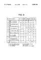
- FIG. 6shows a truth table for DRAM operations in the MPRAM 10. The truth table illustrates logic values supplied to address pins ADD ⁇ 10:9>, ADD ⁇ 8:7>, ADD ⁇ 6:5>, ADD ⁇ 4:0>and BA ⁇ 1:0> for supporting various DRAM operations.
- control signals /RAS and /CASare set to a high level (H) to establish a no-operation mode of the DRAM 12.
- Hhigh level
- the symbol X in the truth tableindicates a "don't care" state of the corresponding address pins, in which they are not required to supply address or command signals. For example, in a no-operation mode of the DRAM 12, pins ADD ⁇ 10:0>, and BA ⁇ 1:0> are in a "don't care" state.
- a precharge command PREis issued. This command is represented by low levels (L) at the address pins ADD ⁇ 10:9>, and ADD ⁇ 6:5>. Pins ADD ⁇ 8:7>, and ADD ⁇ 6:5> are in a don't care state. Pins BA ⁇ 1:0> indicate a valid address (V) for selecting the DRAM bank.
- a precharge command PREAis issued.
- address pins ADD ⁇ 10:9> and ADD ⁇ 6>are set to low levels.
- address pin ADD ⁇ 5>is set to a high level (H).
- pins BA ⁇ 1:0>are in a don't care state.
- a command ACTactivates a row in the idle DRAM bank indicated by the valid bank address at the pins BA ⁇ 1:0>.
- each DRAM bankmay have 512 row addresses.
- Pins ADD ⁇ 8:0>may be used to indicate a 9-bit address RA of the row to be activated.
- Both of unused address pins ADD ⁇ 10:9>may be set to a high level to define the ACT command.
- a DRAM read transfer (DRT) commandis used for transferring one of 32 blocks of data from the DRAM 12 to one of 16 lines in the SRAM 16.
- Address pins ADD ⁇ 10:7>may indicate a 4-bit address S of the SRAM line selected for receiving the data block.
- Address pins ADD ⁇ 4:0>may represent a 5-bit column address CA that indicates the data block selected in the DRAM 12.
- Both address pins ADD ⁇ 6:5>may be set to a low level to define the DRT command.
- a DRAM write transfer (DWT) commandis provided to transfer data from one of 16 lines in the SRAM 16 to one of 32 blocks in the DRAM 12.
- Address pins ADD ⁇ 10:7>may indicate a 4-bit address S of the SRAM line selected for transferring data.
- Address pins ADD ⁇ 4:0>may represent a 5-bit column address CA that indicates the data block selected for receiving the data.
- pin ADD ⁇ 6>may be set to a high level, whereas pin ADD ⁇ 5> may be set to a low level.
- DMTDRAM masked transfer
- An auto-refresh (ARF) commandis used to refresh one row of the DRAM 12.
- ARFauto-refresh
- the address of the row to be refreshedis generated in the DRAM control circuit 42.
- Both address pins ADD ⁇ 6:5>may be set to a low level to represent the ARF command.
- a set mode register (SMR) commandis issued to control MPRAM operations in a programmable burst mode.
- the DRAM control circuit 42may contain programmable mode registers set with the SMR command and supplied with a 5-bit mode register code (MRC) that defines burst type and length.
- the SMR commandmay be represented by a low level at pin ADD ⁇ 5>, and a high level at pin ADD ⁇ 6>.
- Address pins ADD ⁇ 4:0>may carry a 5-bit MRC value to be written in the programmable mode registers.
- the MRC valueis composed of bits A4 to A0.
- Bit A4may be set to 0 and used as a reserved bit.
- Bit A3may define a burst type (BT). For example, when the BT bit is set to 0, data transfer may be carried out in a sequential burst mode. When the BT bit is set to 1, an interleaved burst mode is selected.
- BTburst type
- Bits A2, A1 and A0may be used as a 3-bit burst length (BL) code that defines the length of a data burst. For example, when the BL code is set to 000, burst length is equal to 1. When the BL code is set to 01, burst length is equal to 2, etc.
- BLburst length
- address signals at SRAM address pins ADA and ADBare used to select lines and words in the SRAM 16 during SRAM read and write accesses from ports A and B.
- signals at address pins ADA and ADBmay represent load mask register commands LMRA and LMRB issued to supply mask data into the write per bit (WPB) mask registers 34 and 36, and byte write enable (BWE) mask register 46.
- WPBwrite per bit
- BWEbyte write enable
- the WPB registers 34 and 36 arranged between data ports A and B, and the SRAM 16are used to mask a portion of data being written from ports A and B to the SRAM 16.
- the BWE mask register 46 provided between the DRAM 12 and SRAM 16may mask a byte of data being written from the SRAM 16 to the DRAM 12 in a DRAM masked transfer (DMT) mode.
- DMTDRAM masked transfer
- the WPB registers 34 and 36may be loaded with mask data from either port A or port B.
- the mask dataare supplied via data pins DQA and DQB for loading from ports A and B, respectively.
- SRAM address pins ADA ⁇ 3:0>may carry a 4-bit load mask register command LMRA
- SRAM address pins ADBmay supply a 4-bit load mask register command LMRB.
- the LMRA commandis issued when the WPB or BWE mask register is loaded from port A, whereas the LMRB command controls loading the WPB or BWE mask register from port B.
- Logical value of the LMRA or LMRB commandmay indicate whether the WPB or WRE mask register is being loaded with mask data, and which bits of the mask register are selected for loading. For example, when the LMRA or LMRB command is set to 0000, the 16-bit WPB mask register 34 may be loaded with mask data, whereas the LMRA or LMRB command set to 0001 may request mask data to be written into the 16-bit WPB mask register 36. When the LMRA or LMRB command is set to 0010, mask data may be written into the lower byte of the BWE mask register 46. whereas the LMRA or LMRB command set to 0011 may request mask data to be written into the upper byte of the BWE mask register 46.
- a multi-port memory chiphaving, a DRAM main memory and a SRAM cache memory coupled via a global bus.
- An addressing systemenables the user to perform data transfers between external data ports and the SRAM concurrently with data transfers between the DRAM and the SRAM.
- DRAM address pins on the memory chipselect a data block in the DRAM, and indicates a SRAM line for receiving or transferring data.
- SRAM address pinsdetermine addressed line and word in the SRAM.
- the DRAM address pins and SRAM address pinsare used for supplying commands that define various memory operations.
Landscapes
- Engineering & Computer Science (AREA)
- Theoretical Computer Science (AREA)
- Physics & Mathematics (AREA)
- General Engineering & Computer Science (AREA)
- General Physics & Mathematics (AREA)
- Computer Hardware Design (AREA)
- Dram (AREA)
Abstract
Description
Claims (18)
Priority Applications (1)
| Application Number | Priority Date | Filing Date | Title |
|---|---|---|---|
| US09/018,343US6088760A (en) | 1997-03-07 | 1998-02-04 | Addressing system in a multi-port RAM having main and cache memories |
Applications Claiming Priority (2)
| Application Number | Priority Date | Filing Date | Title |
|---|---|---|---|
| US4005397P | 1997-03-07 | 1997-03-07 | |
| US09/018,343US6088760A (en) | 1997-03-07 | 1998-02-04 | Addressing system in a multi-port RAM having main and cache memories |
Publications (1)
| Publication Number | Publication Date |
|---|---|
| US6088760Atrue US6088760A (en) | 2000-07-11 |
Family
ID=26691008
Family Applications (1)
| Application Number | Title | Priority Date | Filing Date |
|---|---|---|---|
| US09/018,343Expired - LifetimeUS6088760A (en) | 1997-03-07 | 1998-02-04 | Addressing system in a multi-port RAM having main and cache memories |
Country Status (1)
| Country | Link |
|---|---|
| US (1) | US6088760A (en) |
Cited By (41)
| Publication number | Priority date | Publication date | Assignee | Title |
|---|---|---|---|---|
| US6237130B1 (en)* | 1998-10-29 | 2001-05-22 | Nexabit Networks, Inc. | Chip layout for implementing arbitrated high speed switching access of pluralities of I/O data ports to internally cached DRAM banks and the like |
| US6324116B1 (en)* | 1999-06-18 | 2001-11-27 | Samsung Electronics Co., Ltd. | Merged semiconductor device having DRAM and SRAM and data transferring method using the semiconductor device |
| US6327175B1 (en)* | 1999-09-13 | 2001-12-04 | Cypress Semiconductor Corporation | Method and apparatus for controlling a memory array with a programmable register |
| US6339817B1 (en)* | 1997-09-16 | 2002-01-15 | Nec Corporation | Semiconductor memory including main and sub memory portions having plural memory cell groups and a bidirectional data transfer circuit |
| US20020133325A1 (en)* | 2001-02-09 | 2002-09-19 | Hoare Raymond R. | Discrete event simulator |
| US6574130B2 (en) | 2001-07-25 | 2003-06-03 | Nantero, Inc. | Hybrid circuit having nanotube electromechanical memory |
| US6643165B2 (en) | 2001-07-25 | 2003-11-04 | Nantero, Inc. | Electromechanical memory having cell selection circuitry constructed with nanotube technology |
| US6706402B2 (en) | 2001-07-25 | 2004-03-16 | Nantero, Inc. | Nanotube films and articles |
| US6757789B2 (en)* | 1997-10-10 | 2004-06-29 | Rambus, Inc. | Apparatus and method for maximizing information transfers over limited interconnect resources |
| US6779076B1 (en) | 2000-10-05 | 2004-08-17 | Micron Technology, Inc. | Method and system for using dynamic random access memory as cache memory |
| US6784028B2 (en) | 2001-12-28 | 2004-08-31 | Nantero, Inc. | Methods of making electromechanical three-trace junction devices |
| US20040186957A1 (en)* | 2000-08-17 | 2004-09-23 | Brent Keeth | Method and system for using dynamic random access memory as cache memory |
| US20040214367A1 (en)* | 2001-07-25 | 2004-10-28 | Nantero, Inc. | Electromechanical memory array using nanotube ribbons and method for making same |
| US6835591B2 (en) | 2001-07-25 | 2004-12-28 | Nantero, Inc. | Methods of nanotube films and articles |
| US6911682B2 (en) | 2001-12-28 | 2005-06-28 | Nantero, Inc. | Electromechanical three-trace junction devices |
| US20050144371A1 (en)* | 2003-12-30 | 2005-06-30 | Robert Walker | Burst mode implementation in a memory device |
| US20050144372A1 (en)* | 2003-12-31 | 2005-06-30 | Robert Walker | Memory device controlled with user-defined commands |
| US20050268022A1 (en)* | 2004-05-26 | 2005-12-01 | Pelley Perry H | Cache line memory and method therefor |
| US20050268050A1 (en)* | 2004-02-07 | 2005-12-01 | Woon-Sik Suh | Multi-port memory device providing protection signal |
| US20060090056A1 (en)* | 2002-07-10 | 2006-04-27 | Johnson Christopher S | Dynamically setting burst length and type |
| US7176505B2 (en) | 2001-12-28 | 2007-02-13 | Nantero, Inc. | Electromechanical three-trace junction devices |
| US20070211554A1 (en)* | 2004-05-26 | 2007-09-13 | Freescale Semiconductor, Inc. | Memory with serial input-output terminals for address and data and method therefor |
| US7274078B2 (en) | 2001-07-25 | 2007-09-25 | Nantero, Inc. | Devices having vertically-disposed nanofabric articles and methods of making the same |
| US7304357B2 (en) | 2001-07-25 | 2007-12-04 | Nantero, Inc. | Devices having horizontally-disposed nanofabric articles and methods of making the same |
| US20080025127A1 (en)* | 2006-07-12 | 2008-01-31 | Fujitsu Limited | Semiconductor memory, controller, and operating method of semiconductor memory |
| US20080046665A1 (en)* | 2006-05-24 | 2008-02-21 | Kyoung-Park Kim | Multiport Memory Device, Multiprocessor System Including the Same, and Method of Transmitting Data In Multiprocessor System |
| US7335395B2 (en) | 2002-04-23 | 2008-02-26 | Nantero, Inc. | Methods of using pre-formed nanotubes to make carbon nanotube films, layers, fabrics, ribbons, elements and articles |
| US20080148085A1 (en)* | 2006-12-13 | 2008-06-19 | Cypress Semiconductor Corp. | Memory Interface Configurable for Asynchronous and Synchronous Operation and for Accessing Storage from any Clock Domain |
| US20080270714A1 (en)* | 2005-02-14 | 2008-10-30 | Koninklijke Philips Electronics, N.V. | Block Interleaving with Memory Table of Reduced Size |
| US20090150621A1 (en)* | 2007-12-06 | 2009-06-11 | Silicon Image, Inc. | Bank sharing and refresh in a shared multi-port memory device |
| US7560136B2 (en) | 2003-01-13 | 2009-07-14 | Nantero, Inc. | Methods of using thin metal layers to make carbon nanotube films, layers, fabrics, ribbons, elements and articles |
| US7566478B2 (en) | 2001-07-25 | 2009-07-28 | Nantero, Inc. | Methods of making carbon nanotube films, layers, fabrics, ribbons, elements and articles |
| US20100281227A1 (en)* | 2009-04-29 | 2010-11-04 | Micron Technology, Inc. | Multi-port memory devices and methods |
| US20110030064A1 (en)* | 2009-07-31 | 2011-02-03 | Samsung Electronics Co., Ltd. | Data mask system and data mask method |
| US20120221797A1 (en)* | 2011-02-25 | 2012-08-30 | Chung Moo-Kyoung | Multi-port cache memory apparatus and method |
| US9353224B2 (en) | 2013-08-26 | 2016-05-31 | Samsung Electronics Co., Ltd. | Poly(imide-amide) copolymer and composition including poly(imide-amide) copolymer |
| US9388279B2 (en) | 2013-08-26 | 2016-07-12 | Samsung Electronics Co., Ltd. | Poly(imide-amide) copolymer, a method of preparing a poly(imide-amide) copolymer, and an article including a poly(imide-amide) copolymer |
| US20180173588A1 (en)* | 2015-06-30 | 2018-06-21 | Hewlett-Packard Development Company, L.P. | Patrol Scrub Periods Based on Power Status |
| US20180314591A1 (en)* | 2015-12-08 | 2018-11-01 | Nvidia Corporation | Controller-based memory scrub for drams with internal error-correcting code (ecc) bits contemporaneously during auto refresh or by using masked write commands |
| US20220199127A1 (en)* | 2020-12-17 | 2022-06-23 | Micron Technology, Inc. | Transferring data between dram and sram |
| CN118153511A (en)* | 2024-05-09 | 2024-06-07 | 南京齐芯半导体有限公司 | Optimized layout method and module for changing data bit position in time |
Citations (4)
| Publication number | Priority date | Publication date | Assignee | Title |
|---|---|---|---|---|
| US5544121A (en)* | 1991-04-18 | 1996-08-06 | Mitsubishi Denki Kabushiki Kaisha | Semiconductor memory device |
| US5546343A (en)* | 1990-10-18 | 1996-08-13 | Elliott; Duncan G. | Method and apparatus for a single instruction operating multiple processors on a memory chip |
| US5561781A (en)* | 1993-07-28 | 1996-10-01 | International Business Machines Corporation | Port swapping for improved virtual SRAM performance and processing of concurrent processor access requests |
| US5566318A (en)* | 1994-08-02 | 1996-10-15 | Ramtron International Corporation | Circuit with a single address register that augments a memory controller by enabling cache reads and page-mode writes |
- 1998
- 1998-02-04USUS09/018,343patent/US6088760A/ennot_activeExpired - Lifetime
Patent Citations (4)
| Publication number | Priority date | Publication date | Assignee | Title |
|---|---|---|---|---|
| US5546343A (en)* | 1990-10-18 | 1996-08-13 | Elliott; Duncan G. | Method and apparatus for a single instruction operating multiple processors on a memory chip |
| US5544121A (en)* | 1991-04-18 | 1996-08-06 | Mitsubishi Denki Kabushiki Kaisha | Semiconductor memory device |
| US5561781A (en)* | 1993-07-28 | 1996-10-01 | International Business Machines Corporation | Port swapping for improved virtual SRAM performance and processing of concurrent processor access requests |
| US5566318A (en)* | 1994-08-02 | 1996-10-15 | Ramtron International Corporation | Circuit with a single address register that augments a memory controller by enabling cache reads and page-mode writes |
Cited By (93)
| Publication number | Priority date | Publication date | Assignee | Title |
|---|---|---|---|---|
| US6339817B1 (en)* | 1997-09-16 | 2002-01-15 | Nec Corporation | Semiconductor memory including main and sub memory portions having plural memory cell groups and a bidirectional data transfer circuit |
| US6757789B2 (en)* | 1997-10-10 | 2004-06-29 | Rambus, Inc. | Apparatus and method for maximizing information transfers over limited interconnect resources |
| US6237130B1 (en)* | 1998-10-29 | 2001-05-22 | Nexabit Networks, Inc. | Chip layout for implementing arbitrated high speed switching access of pluralities of I/O data ports to internally cached DRAM banks and the like |
| US6324116B1 (en)* | 1999-06-18 | 2001-11-27 | Samsung Electronics Co., Ltd. | Merged semiconductor device having DRAM and SRAM and data transferring method using the semiconductor device |
| US6327175B1 (en)* | 1999-09-13 | 2001-12-04 | Cypress Semiconductor Corporation | Method and apparatus for controlling a memory array with a programmable register |
| US20070055818A1 (en)* | 2000-08-17 | 2007-03-08 | Micron Technology, Inc. | Method and system for using dynamic random access memory as cache memory |
| US20080177943A1 (en)* | 2000-08-17 | 2008-07-24 | Micron Technology, Inc. | Method and system for using dynamic random access memory as cache memory |
| US7350018B2 (en) | 2000-08-17 | 2008-03-25 | Micron Technology, Inc. | Method and system for using dynamic random access memory as cache memory |
| US7917692B2 (en) | 2000-08-17 | 2011-03-29 | Round Rock Research, Llc | Method and system for using dynamic random access memory as cache memory |
| US20040186957A1 (en)* | 2000-08-17 | 2004-09-23 | Brent Keeth | Method and system for using dynamic random access memory as cache memory |
| US6948027B2 (en) | 2000-08-17 | 2005-09-20 | Micron Technology, Inc. | Method and system for using dynamic random access memory as cache memory |
| US7155561B2 (en) | 2000-08-17 | 2006-12-26 | Micron Technology, Inc. | Method and system for using dynamic random access memory as cache memory |
| US20060015679A1 (en)* | 2000-08-17 | 2006-01-19 | Brent Keeth | Method and system for using dynamic random access memory as cache memory |
| US6862654B1 (en) | 2000-08-17 | 2005-03-01 | Micron Technology, Inc. | Method and system for using dynamic random access memory as cache memory |
| US6779076B1 (en) | 2000-10-05 | 2004-08-17 | Micron Technology, Inc. | Method and system for using dynamic random access memory as cache memory |
| US6965536B2 (en) | 2000-10-05 | 2005-11-15 | Micron Technology, Inc. | Method and system for using dynamic random access memory as cache memory |
| US20050007848A1 (en)* | 2000-10-05 | 2005-01-13 | Shirley Brian M. | Method and system for using dynamic random access memory as cache memory |
| US20020133325A1 (en)* | 2001-02-09 | 2002-09-19 | Hoare Raymond R. | Discrete event simulator |
| US7342818B2 (en) | 2001-07-25 | 2008-03-11 | Nantero, Inc. | Hybrid circuit having nanotube electromechanical memory |
| US7056758B2 (en) | 2001-07-25 | 2006-06-06 | Nantero, Inc. | Electromechanical memory array using nanotube ribbons and method for making same |
| US8101976B2 (en) | 2001-07-25 | 2012-01-24 | Nantero Inc. | Device selection circuitry constructed with nanotube ribbon technology |
| US6574130B2 (en) | 2001-07-25 | 2003-06-03 | Nantero, Inc. | Hybrid circuit having nanotube electromechanical memory |
| US6919592B2 (en) | 2001-07-25 | 2005-07-19 | Nantero, Inc. | Electromechanical memory array using nanotube ribbons and method for making same |
| US6942921B2 (en) | 2001-07-25 | 2005-09-13 | Nantero, Inc. | Nanotube films and articles |
| US20050063210A1 (en)* | 2001-07-25 | 2005-03-24 | Nantero, Inc. | Hybrid circuit having nanotube electromechanical memory |
| US6835591B2 (en) | 2001-07-25 | 2004-12-28 | Nantero, Inc. | Methods of nanotube films and articles |
| US6706402B2 (en) | 2001-07-25 | 2004-03-16 | Nantero, Inc. | Nanotube films and articles |
| US7745810B2 (en) | 2001-07-25 | 2010-06-29 | Nantero, Inc. | Nanotube films and articles |
| US7304357B2 (en) | 2001-07-25 | 2007-12-04 | Nantero, Inc. | Devices having horizontally-disposed nanofabric articles and methods of making the same |
| US6836424B2 (en) | 2001-07-25 | 2004-12-28 | Nantero, Inc. | Hybrid circuit having nanotube electromechanical memory |
| US7566478B2 (en) | 2001-07-25 | 2009-07-28 | Nantero, Inc. | Methods of making carbon nanotube films, layers, fabrics, ribbons, elements and articles |
| US7335528B2 (en) | 2001-07-25 | 2008-02-26 | Nantero, Inc. | Methods of nanotube films and articles |
| US7298016B2 (en) | 2001-07-25 | 2007-11-20 | Nantero, Inc. | Electromechanical memory array using nanotube ribbons and method for making same |
| US7120047B2 (en) | 2001-07-25 | 2006-10-10 | Segal Brent M | Device selection circuitry constructed with nanotube technology |
| US7274078B2 (en) | 2001-07-25 | 2007-09-25 | Nantero, Inc. | Devices having vertically-disposed nanofabric articles and methods of making the same |
| US20040214367A1 (en)* | 2001-07-25 | 2004-10-28 | Nantero, Inc. | Electromechanical memory array using nanotube ribbons and method for making same |
| US6643165B2 (en) | 2001-07-25 | 2003-11-04 | Nantero, Inc. | Electromechanical memory having cell selection circuitry constructed with nanotube technology |
| US7264990B2 (en) | 2001-07-25 | 2007-09-04 | Nantero, Inc. | Methods of nanotubes films and articles |
| US20040191978A1 (en)* | 2001-12-28 | 2004-09-30 | Nantero, Inc. | Methods of making electromechanical three-trace junction devices |
| US7176505B2 (en) | 2001-12-28 | 2007-02-13 | Nantero, Inc. | Electromechanical three-trace junction devices |
| US7521736B2 (en) | 2001-12-28 | 2009-04-21 | Nantero, Inc. | Electromechanical three-trace junction devices |
| US6911682B2 (en) | 2001-12-28 | 2005-06-28 | Nantero, Inc. | Electromechanical three-trace junction devices |
| US6979590B2 (en) | 2001-12-28 | 2005-12-27 | Nantero, Inc. | Methods of making electromechanical three-trace junction devices |
| US7915066B2 (en) | 2001-12-28 | 2011-03-29 | Nantero, Inc. | Methods of making electromechanical three-trace junction devices |
| US6784028B2 (en) | 2001-12-28 | 2004-08-31 | Nantero, Inc. | Methods of making electromechanical three-trace junction devices |
| US7335395B2 (en) | 2002-04-23 | 2008-02-26 | Nantero, Inc. | Methods of using pre-formed nanotubes to make carbon nanotube films, layers, fabrics, ribbons, elements and articles |
| US8281052B2 (en) | 2002-07-10 | 2012-10-02 | Round Rock Research, Llc | Dynamically setting burst length of double data rate memory device by applying signal to at least one external pin during a read or write transaction |
| US7984207B2 (en) | 2002-07-10 | 2011-07-19 | Round Rock Research, Llc | Dynamically setting burst length of double data rate memory device by applying signal to at least one external pin during a read or write transaction |
| US8019913B2 (en) | 2002-07-10 | 2011-09-13 | Round Rock Research, Llc | Dynamically setting burst length of double data rate memory device by applying signal to at least one external pin during a read or write transaction |
| US20090307446A1 (en)* | 2002-07-10 | 2009-12-10 | Johnson Christopher S | Dynamically setting burst length of a double data rate memory device |
| US8156262B2 (en) | 2002-07-10 | 2012-04-10 | Round Rock Research, Llc | Dynamically setting burst length of double data rate memory device by applying signal to at least one external pin during a read or write transaction |
| US7603493B2 (en) | 2002-07-10 | 2009-10-13 | Micron Technology, Inc. | Dynamically setting burst length of memory device by applying signal to at least one external pin during a read or write transaction |
| US20060090056A1 (en)* | 2002-07-10 | 2006-04-27 | Johnson Christopher S | Dynamically setting burst length and type |
| US7149824B2 (en)* | 2002-07-10 | 2006-12-12 | Micron Technology, Inc. | Dynamically setting burst length of memory device by applying signal to at least one external pin during a read or write transaction |
| US7560136B2 (en) | 2003-01-13 | 2009-07-14 | Nantero, Inc. | Methods of using thin metal layers to make carbon nanotube films, layers, fabrics, ribbons, elements and articles |
| US20050144371A1 (en)* | 2003-12-30 | 2005-06-30 | Robert Walker | Burst mode implementation in a memory device |
| US7111143B2 (en)* | 2003-12-30 | 2006-09-19 | Infineon Technologies Ag | Burst mode implementation in a memory device |
| US20050144372A1 (en)* | 2003-12-31 | 2005-06-30 | Robert Walker | Memory device controlled with user-defined commands |
| US20050268050A1 (en)* | 2004-02-07 | 2005-12-01 | Woon-Sik Suh | Multi-port memory device providing protection signal |
| US7474585B2 (en) | 2004-05-26 | 2009-01-06 | Freescale Semiconductor, Inc. | Memory with serial input-output terminals for address and data and method therefor |
| US20050268022A1 (en)* | 2004-05-26 | 2005-12-01 | Pelley Perry H | Cache line memory and method therefor |
| US20070211554A1 (en)* | 2004-05-26 | 2007-09-13 | Freescale Semiconductor, Inc. | Memory with serial input-output terminals for address and data and method therefor |
| US7840859B2 (en) | 2005-02-14 | 2010-11-23 | Koninklijke Philips Electronics N.V. | Block interleaving with memory table of reduced size |
| US20080270714A1 (en)* | 2005-02-14 | 2008-10-30 | Koninklijke Philips Electronics, N.V. | Block Interleaving with Memory Table of Reduced Size |
| US20080046665A1 (en)* | 2006-05-24 | 2008-02-21 | Kyoung-Park Kim | Multiport Memory Device, Multiprocessor System Including the Same, and Method of Transmitting Data In Multiprocessor System |
| US7684258B2 (en)* | 2006-07-12 | 2010-03-23 | Fujitsu Microelectronics Limited | Semiconductor memory and controller with time-shared mode for row address, column address and data mask signals inputted via address terminals |
| US20080025127A1 (en)* | 2006-07-12 | 2008-01-31 | Fujitsu Limited | Semiconductor memory, controller, and operating method of semiconductor memory |
| US9734877B2 (en) | 2006-12-13 | 2017-08-15 | Cypress Semiconductor Corporation | Memory interface configurable for asynchronous and synchronous operation and for accessing storage from any clock |
| US20080148085A1 (en)* | 2006-12-13 | 2008-06-19 | Cypress Semiconductor Corp. | Memory Interface Configurable for Asynchronous and Synchronous Operation and for Accessing Storage from any Clock Domain |
| US8266405B2 (en) | 2006-12-13 | 2012-09-11 | Cypress Semiconductor Corporation | Memory interface configurable for asynchronous and synchronous operation and for accessing storage from any clock domain |
| US10456819B2 (en) | 2006-12-13 | 2019-10-29 | Cypress Semiconductor Corporation | Memory interface configurable for asynchronous and synchronous operation and for accessing storage from any clock domain |
| US20090150621A1 (en)* | 2007-12-06 | 2009-06-11 | Silicon Image, Inc. | Bank sharing and refresh in a shared multi-port memory device |
| WO2009073331A1 (en)* | 2007-12-06 | 2009-06-11 | Silicon Image, Inc. | Bank sharing and refresh in a shared multi-port memory device |
| US8001334B2 (en) | 2007-12-06 | 2011-08-16 | Silicon Image, Inc. | Bank sharing and refresh in a shared multi-port memory device |
| US8930642B2 (en) | 2009-04-29 | 2015-01-06 | Micron Technology, Inc. | Configurable multi-port memory device and method thereof |
| US20100281227A1 (en)* | 2009-04-29 | 2010-11-04 | Micron Technology, Inc. | Multi-port memory devices and methods |
| TWI484498B (en)* | 2009-04-29 | 2015-05-11 | Micron Technology Inc | Multi-port memory devices and methods |
| US8250312B2 (en)* | 2009-04-29 | 2012-08-21 | Micron Technology, Inc. | Configurable multi-port memory devices and methods |
| US8677082B2 (en) | 2009-07-31 | 2014-03-18 | Samsung Electronics Co., Ltd. | Data mask system and data mask method |
| US8321640B2 (en)* | 2009-07-31 | 2012-11-27 | Samsung Electronics Co., Ltd. | Data mask system and data mask method |
| US20110030064A1 (en)* | 2009-07-31 | 2011-02-03 | Samsung Electronics Co., Ltd. | Data mask system and data mask method |
| US20120221797A1 (en)* | 2011-02-25 | 2012-08-30 | Chung Moo-Kyoung | Multi-port cache memory apparatus and method |
| US8977800B2 (en)* | 2011-02-25 | 2015-03-10 | Samsung Electronics Co., Ltd. | Multi-port cache memory apparatus and method |
| US9353224B2 (en) | 2013-08-26 | 2016-05-31 | Samsung Electronics Co., Ltd. | Poly(imide-amide) copolymer and composition including poly(imide-amide) copolymer |
| US9388279B2 (en) | 2013-08-26 | 2016-07-12 | Samsung Electronics Co., Ltd. | Poly(imide-amide) copolymer, a method of preparing a poly(imide-amide) copolymer, and an article including a poly(imide-amide) copolymer |
| US10521294B2 (en)* | 2015-06-30 | 2019-12-31 | Hewlett-Packard Development Company, L.P. | Patrol scrub periods based on power status |
| US20180173588A1 (en)* | 2015-06-30 | 2018-06-21 | Hewlett-Packard Development Company, L.P. | Patrol Scrub Periods Based on Power Status |
| US10445177B2 (en)* | 2015-12-08 | 2019-10-15 | Nvidia Corporation | Controller-based memory scrub for DRAMs with internal error-correcting code (ECC) bits contemporaneously during auto refresh or by using masked write commands |
| US20180314591A1 (en)* | 2015-12-08 | 2018-11-01 | Nvidia Corporation | Controller-based memory scrub for drams with internal error-correcting code (ecc) bits contemporaneously during auto refresh or by using masked write commands |
| US20220199127A1 (en)* | 2020-12-17 | 2022-06-23 | Micron Technology, Inc. | Transferring data between dram and sram |
| US11380372B1 (en)* | 2020-12-17 | 2022-07-05 | Micron Technology, Inc. | Transferring data between DRAM and SRAM |
| US11837315B2 (en) | 2020-12-17 | 2023-12-05 | Micron Technology, Inc. | Transferring data between DRAM and SRAM |
| CN118153511A (en)* | 2024-05-09 | 2024-06-07 | 南京齐芯半导体有限公司 | Optimized layout method and module for changing data bit position in time |
Similar Documents
| Publication | Publication Date | Title |
|---|---|---|
| US6088760A (en) | Addressing system in a multi-port RAM having main and cache memories | |
| US6167487A (en) | Multi-port RAM having functionally identical ports | |
| US5555528A (en) | Dynamic random access memory persistent page implemented as processor register sets | |
| US4577293A (en) | Distributed, on-chip cache | |
| US8255622B2 (en) | Memory controller and data processing system | |
| US5184320A (en) | Cached random access memory device and system | |
| US5590078A (en) | Method of and apparatus for improved dynamic random access memory (DRAM) providing increased data bandwidth and addressing range for current DRAM devices and/or equivalent bandwidth and addressing range for smaller DRAM devices | |
| US8369168B2 (en) | Devices and system providing reduced quantity of interconnections | |
| KR100393860B1 (en) | Random access memory | |
| JPH11265315A (en) | High-speed and compact address bit route specifying mechanism for supporting various dram bank sizes and plural interleaving mechanisms | |
| JPH0652633B2 (en) | Memory subsystem | |
| US6101579A (en) | Multi-port memory device having masking registers | |
| US5946262A (en) | RAM having multiple ports sharing common memory locations | |
| US6754135B2 (en) | Reduced latency wide-I/O burst architecture | |
| JP3094956B2 (en) | Semiconductor storage device | |
| US5802586A (en) | Cache memory having a read-modify-write operation and simultaneous burst read and write operations and a method therefor | |
| US6157990A (en) | Independent chip select for SRAM and DRAM in a multi-port RAM | |
| KR20030096265A (en) | Dram and access method | |
| US5559749A (en) | Multi-bit block write in a random access memory | |
| US5959937A (en) | Dual clocking scheme in a multi-port RAM | |
| JP3863280B2 (en) | Memory device, SRAM cell, and data transfer method | |
| US6631441B2 (en) | DRAM read and write circuit | |
| US11983113B2 (en) | Method for copying data within memory device, memory device, and electronic device thereof | |
| JPH10326486A (en) | Memory unit, and data transfer method |
Legal Events
| Date | Code | Title | Description |
|---|---|---|---|
| AS | Assignment | Owner name:MITSUBISHI SEMICONDUCTOR AMERICA, INC., NORTH CARO Free format text:ASSIGNMENT OF ASSIGNORS INTEREST;ASSIGNORS:WALKER, ROBERT M.;CAMACHO, STEPHEN;CASSADA, RHONDA;REEL/FRAME:008977/0570 Effective date:19980129 | |
| AS | Assignment | Owner name:MITSUBISHI ELECTRONICS AMERICA, INC., CALIFORNIA Free format text:ASSIGNMENT OF ASSIGNORS INTEREST;ASSIGNOR:MITSUBISHI SEMICONDUCTOR AMERICA, INC.;REEL/FRAME:009958/0191 Effective date:19981211 | |
| STCF | Information on status: patent grant | Free format text:PATENTED CASE | |
| FPAY | Fee payment | Year of fee payment:4 | |
| REMI | Maintenance fee reminder mailed | ||
| SULP | Surcharge for late payment | ||
| FPAY | Fee payment | Year of fee payment:8 | |
| AS | Assignment | Owner name:MITSUBISHI ELECTRIC & ELECTRONICS USA, INC., CALIF Free format text:ASSIGNMENT OF ASSIGNORS INTEREST;ASSIGNOR:MITSUBISHI ELECTRONICS AMERICA, INC.;REEL/FRAME:021794/0916 Effective date:20081106 | |
| AS | Assignment | Owner name:HITACHI SEMICONDUCTOR (AMERICA) INC., CALIFORNIA Free format text:ASSIGNMENT OF ASSIGNORS INTEREST;ASSIGNOR:MITSUBISHI ELECTRIC AND ELECTRONICS USA, INC.;REEL/FRAME:021890/0528 Effective date:20030331 Owner name:RENESAS TECHNOLOGY AMERICA, INC., CALIFORNIA Free format text:CHANGE OF NAME;ASSIGNOR:HITACHI SEMICONDUCTOR (AMERICA) INC.;REEL/FRAME:021890/0874 Effective date:20030331 | |
| AS | Assignment | Owner name:RENESAS ELECTRONICS AMERICA INC.,CALIFORNIA Free format text:MERGER;ASSIGNOR:RENESAS TECHNOLOGY AMERICA, INC.;REEL/FRAME:024380/0300 Effective date:20100401 | |
| FEPP | Fee payment procedure | Free format text:PAYOR NUMBER ASSIGNED (ORIGINAL EVENT CODE: ASPN); ENTITY STATUS OF PATENT OWNER: LARGE ENTITY | |
| FPAY | Fee payment | Year of fee payment:12 | |
| SULP | Surcharge for late payment | Year of fee payment:11 |