US6085334A - Method and apparatus for testing an integrated memory device - Google Patents
Method and apparatus for testing an integrated memory deviceDownload PDFInfo
- Publication number
- US6085334A US6085334AUS09/061,983US6198398AUS6085334AUS 6085334 AUS6085334 AUS 6085334AUS 6198398 AUS6198398 AUS 6198398AUS 6085334 AUS6085334 AUS 6085334A
- Authority
- US
- United States
- Prior art keywords
- memory
- signature
- built
- self
- repair
- Prior art date
- Legal status (The legal status is an assumption and is not a legal conclusion. Google has not performed a legal analysis and makes no representation as to the accuracy of the status listed.)
- Expired - Fee Related
Links
Images

Classifications
- G—PHYSICS
- G11—INFORMATION STORAGE
- G11C—STATIC STORES
- G11C29/00—Checking stores for correct operation ; Subsequent repair; Testing stores during standby or offline operation
- G11C29/04—Detection or location of defective memory elements, e.g. cell constructio details, timing of test signals
- G11C29/08—Functional testing, e.g. testing during refresh, power-on self testing [POST] or distributed testing
- G11C29/12—Built-in arrangements for testing, e.g. built-in self testing [BIST] or interconnection details
- G11C29/38—Response verification devices
- G11C29/40—Response verification devices using compression techniques
- G—PHYSICS
- G06—COMPUTING OR CALCULATING; COUNTING
- G06F—ELECTRIC DIGITAL DATA PROCESSING
- G06F11/00—Error detection; Error correction; Monitoring
- G06F11/006—Identification
Definitions
- the present inventionrelates generally to integrated memory testing and more particularly to the built-in self-test and self-repair of memory devices.
- a typical memory deviceis composed of a plurality of memory elements or cells defining a memory array, and may contain a plurality of memory arrays.
- a memory cell in the memory arrayis accessed by row and column locations.
- each cellwill have an associated address and a row decoder will be used to select the row portion of the address while a column decoder will select the column of the cell.
- the memory arraymay include redundant elements for use as replacement elements for defects.
- the redundant elementsare effectively spare elements. Redundant elements are allocated either as a row or as a column. For example, in a memory device having only row redundancy, if any cell in a row is defective, the entire row of cells will be replaced. Redundant elements may be arranged in a global or a local fashion. Local redundant elements are provided per memory array and cannot be applied to other memory arrays within a memory system. Global redundant elements are available for replacement of elements within any memory array in the memory system.
- a predetermined test pattern sequenceis used to test each cell in the memory.
- the patternmay include any number of steps, each step consisting of a number of read/write sequences.
- a typical test methodinitially writes a first value to a memory cell to be tested. The test then reads that memory cell to verify that the value is stored in the memory cell. The test then writes a second value to the memory cell, where the second value is the complement of the first value. Storage of the second value is then verified. If the memory cell fails any step within the test method, the memory cell is considered defective.
- the testing of memorymay be performed by an external tester, such as an automatic test equipment (ATE), or may be performed internally in the memory device. Internal testing is referred to as built-in self-test (BIST).
- ATEautomatic test equipment
- repairreplacement of a defective cell with a spare row, or redundant element, is referred to as a repair.
- a row repair of a memory cellinvolves configuring the address input to select the spare row instead of the defective row. In effect, the spare row replaces the row containing the defective cell.
- the redundant elementis a column, and the entire column containing the defective cell is replaced. Repair of the memory array may also be performed externally to the memory device, where the defective cells are tested and recorded or marked, and then a permanent replacement is made to redundant elements.
- One method of repairinvolves laser repair, which creates an open circuit to program a redundant element to respond to the address of the defective cell.
- the lasereffects programming by selectively cutting a metal trace coupled to the address logic of the defective cell.
- the additional circuitry required to facilitate such programming and the additional production step to perform laser cuttingresult in additional cost.
- Memory cell repairmay be performed internally by a built-in self-repair (BISR) circuit.
- the BISRis typically used in conjunction with the BIST, but facilitates repair internally, without the use of external methods, such as laser cutting.
- the BISRperforms an electrical repair, which may be permanent or temporary.
- a permanent repairuses non-volatile technology, such as electrically erasable programmable memory, one time programmable memory (OTP), or flash memory. Incorporation of non-volatile memory technology strictly for repair functions is cost prohibitive and is not often considered unless the integrated circuit device has already included this technology for other features.
- Temporary repairutilizes conventional logic and may be implemented without additional fabrication steps.
- Temporary repairoffers a cost effective method of replacement, but the repairs must be made each time the device is powered up. This is true during production testing, and continues throughout the life of the device. The user must continue to repair any defective memory cells every time the device is powered up.
- a drawback associated with temporary repairis the lack of certainty that the same repairs will be made to the device in a user's system as were made in production testing. The concern is that environmental changes may have an effect on the operation of memory cells. Environmental conditions include operating voltage, temperature, frequency of the device, etc.
- production testingmay discover a failure that occurs in a given environmental condition, such as at high temperature.
- the failuremay be repaired by replacing the defective memory cell, so the memory device is not rejected.
- the userperforms the BISR at room temperature, where the user's environmental condition does not cause the high temperature failure, the BISR will not repair the defective cell.
- the user's systemlater encounters the original environmental condition that caused the failure in production testing, i.e. high temperature, the memory cell will fail.
- There is a need for detecting memory device defectswhere the defects are sensitive to environmental conditions and are not exhibited over the entire operating range of the device.
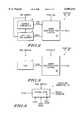
- FIG. 1illustrates, in block diagram form, a data processing system according to an embodiment of the present invention
- FIGS. 2 and 3illustrate, in block diagram form, error qualifier 38 of FIG. 1, according to embodiments of the present invention
- FIG. 4illustrates, in block diagram form, signature generator 32 of FIG. 1, according to an embodiment of the present invention.
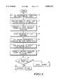
- FIG. 5illustrates, in flow diagram form, a process of memory repair monitoring according to one embodiment of the present invention.
- a method of memory testdetects defects in a memory array which are sensitive to environmental conditions.
- An environmentally sensitive defectis characterized by any change in the repair state of the memory device over the operating range of the memory device.
- the methodgenerates a signature value to reflect the repair state of the memory device at a first operating condition and generates a second signature value to reflect the repair state of the memory device at a second operating condition.
- Environmentally sensitive defectsare detected when the second signature value is different from the original signature value. Effectively, a memory device is rejected if there is a change in the repair state of the memory array over the operating range of the device.
- buswill be used to refer to a plurality of signals or conductors which may be used to transfer one or more various types of information, such as data, addresses, control, or status.
- assertand “negate” will be used when referring to the rendering of a signal, status bit, or similar apparatus into its logically true (i.e. active or asserted) or logically false (i.e. inactive or negated) state, respectively. If the logically true state is a logic level one, the logically false state will be a logic level zero. And if the logically true state is a logic level zero, the logically false state will be a logic level one.
- an integrated circuitincludes a memory array; a plurality of spare memory elements for repairing defective locations of the memory array; a built-in self-test circuit, coupled to the memory array, for detecting faults in the memory array, and in response to detecting a fault, storing an address corresponding to a failed memory location that caused the fault and producing an output signal indicating when a fault is detected; a built-in self-repair circuit, coupled to the memory array, for causing the failed memory location of the memory array to be replaced with a spare memory element of the plurality of spare memory elements; and a built-in self-repair monitoring circuit, coupled to the built-in self-test circuit, for generating a signature based on a compression of addresses corresponding to failed memory locations, wherein the signature is used to determine that a repair result of the memory array is invariant over different environmental conditions.
- a data processing systemincludes a central processing unit; a memory array, coupled to the central processing unit, for storing information for use by the central processing unit; a plurality of spare memory elements for repairing defective locations of the memory array; a built-in self-test circuit, coupled to the memory array, for selectively detecting defects in the memory array, and in response to detecting a defect, providing an address corresponding to a defective memory location and producing an output signal for indicating when a defect is detected; a built-in self-repair circuit, coupled to the memory array, for selectively causing a defective memory location of the memory array to be repaired with a spare memory element of the plurality of spare memory elements; and a built-in self-repair monitoring circuit, coupled to the built-in self-test circuit, for generating a signature based on a compression of addresses corresponding to defective memory locations, wherein the signature is used to determine that a repair result of the memory array is invariant over different environmental conditions.
- a method for testing and repairing an embedded memory in an integrated circuitincludes the steps of: (i) setting a first predetermined environmental condition for testing the embedded memory; (ii) activating a built-in self-test circuit and a built-in self-repair circuit to detect and repair faulty memory cells of the embedded memory under the first predetermined environmental condition; (iii) generating a first signature based on addresses of the faulty memory cells determined during testing under the first predetermined environmental condition; (iv) providing the first signature to a first storage location; (v) setting a second predetermined environmental condition for testing the embedded memory; (vi) clearing results of detecting and repairing faulty memory cells under the first predetermined environmental condition; (vii) activating the built-in self-test circuit and the built-in self-repair circuit to detect and repair faulty memory cells of the embedded memory under the second predetermined environmental condition; (viii) generating a second signature based on addresses of the faulty memory cells determined during testing under the second predetermined environmental condition; (ix
- FIG. 1illustrates data processing system 5 according to one embodiment of the present invention.
- Data processing system 5includes a central processing unit (CPU) 15, BIST 30, BISR monitoring circuit 31, memory 41, memory controller 20, memory interface 37 and BISR circuit 39.
- CPU 15is coupled to memory interface 37 by way of address bus 6 and data bus 7.
- Memory controller 20is coupled to CPU 15 by way of multiple conductors.
- Memory controller 20provides a control signal to memory interface 37 by way of conductors 8.
- Memory 41is a memory having redundant spare elements, such as found in a dynamic random access memory (DRAM) or a static random access memory (SRAM).
- DRAMdynamic random access memory
- SRAMstatic random access memory
- Memory interface 37is used to multiplex address, data and control between CPU 15 and BIST 30. For normal operation, memory interface 37 receives address information from CPU 15 via address bus 6 and transfers that information to memory 41 via address bus 9. According to one embodiment, addresses busses 6 and 9 are unidirectional multiconductor busses. Similarly, memory interface 37 communicates data information with CPU 15 via bidirectional data bus 7 and with memory 41 via bidirectional data bus 11. Memory controller 20 monitors operation of CPU 15 and provides control signals to memory interface 37 via conductors 8, where the control signals provide information necessary for communication with memory 41 via conductors 13. Control signals include any number of signals, such as a read/write (R/W) indicator, a chip select signal (CS), a row address strobe (RAS), and column address strobe (CAS).
- R/Wread/write
- CSchip select signal
- RASrow address strobe
- CAScolumn address strobe
- Memory interface 37receives a GOBIST signal to initiate internal memory testing. In response to the GOBIST signal, memory interface 37 receives address information from BIST 30 via address bus 17. Memory interface 37 communicates data information via data bus 19 and control information via conductors 21. During BIST operation address is provided to memory 41 via address bus 9, data is communicated with memory 41 via data bus 11, and control information is provided by conductors 13. BIST 30 is an internal testing unit used to detect defects in memory array 40. BIST 30 includes address generator 36 and data compare 34. During BIST operation, address generator 36 generates an address to be tested. According to one embodiment, BIST tests rows sequentially starting with an initial row and sequencing through the entire array. The address to be tested is provided to memory interface 37, which conveys the information to memory 41.
- BISR monitoring circuit 31includes error qualifier 38 and signature generator 32.
- Address generator 36provides row address information to error qualifier 38.
- the row address informationis the portion of the address identifying the row of the address under test.
- Error qualifier 38also receives pass/fail information from data compare 34.
- error qualifier 38compares the row address received from address generator 36 to a fail history of memory array 40. If there is a match, error qualifier 38 ignores the fail indication by negating the QFAIL signal. However, if there is no match detected, error qualifier 38 asserts the signal QFAIL, which indicates a first failure of this row.
- QFAILis provided to signature generator 32, which creates a repair signature, where the repair signature is based on a compression of those rows which resulted in assertion of QFAIL.
- the repair signatureis initialized to a start value and is thereafter updated each time QFAIL is asserted during BIST/BISR operation.
- the repair signaturereflects the repair state of memory array 40 at completion of BIST/BISR operation.
- the repair stateis a characteristic of the defective rows replaced during this repair cycle.
- the repair signatureis a surrogate of the repair state of memory 41.
- Data compare 34is coupled to memory interface 37 by way of a bidirectional data bus 19. Data compare 34 generates memory input data to be used during BIST testing and verifies the memory output data at the address under test. When an error is detected, data compare 34 provides a fail indication to error qualifier 38, and provides a repair signal to BISR circuit 39. BISR circuit 39 is coupled to row decoder logic 46. Memory array 40 is coupled to row decoder logic 46 and column logic 44. At least one spare row is located within memory array 40, and may be located adjacent to memory array 40. Row decoder logic 46 and column logic 44 are responsive to address information received from memory interface 37. Each cell within memory array 40 is identified by a row and column location. When memory array 40 receives address information from memory interface 37, row decoder logic 46 decodes the row of that address and column logic decodes the column of the address.
- BISR circuit 39When the REPAIR signal is asserted, BISR circuit 39 replaces the row containing the defective memory cell with an available row from spare row 42. BISR circuit 39 is able to replace as many defective rows of memory array 40 as there are spare rows for replacement for memory array 40. In one embodiment, BISR circuit 39 alters a repair bit to modify the behavior of row decoder logic 46, such that a spare row 42 of memory 41 is allocated to respond to the defective row address. In another embodiment, BISR circuit 39 includes a content addressable memory (CAM) and a spare row of memory cells; BISR circuit 39 enters an address of a memory row into the CAM, where each location in the CAM has a corresponding allocated spare row of memory cells. In this embodiment, data is multiplexed from memory 41 or spare rows 42 onto data bus 11, and address information is provided from memory interface 37 to BISR circuit 39.
- CAMcontent addressable memory
- BIST 30performs memory testing for each row of memory array 40. As a defective memory cell is detected, the memory row is replaced. During production, testing will often test the memory device over a range of operating conditions. If the signature generated on any iteration of the BIST/BISR process differs from a previous signature, the device is rejected. The signature generation and confirmation checks for repeatability of repair ensuring consistent, correct operation of the memory device.
- REPAIR SIGNATUREis a serial output of BISR monitoring circuit 31.
- REPAIR SIGNATUREis a multiple bit signal provided in parallel on multiple conductors.
- FIG. 2illustrates an embodiment of error qualifier 38 of FIG. 1.
- Row address informationis provided to address comparator 54 by address generator 36.
- Last fail row address 52stores the address of the last failing row.
- Row address informationis provided to last fail row address 52 from address generator 36, and is updated in response to an UPDATE signal received from error identification control 50.
- address comparator 54compares the address of the present row under test to the address stored in the last fail row address 52. If the current row address and the last fail row address match, no error identification is indicated and the FIRST FAIL signal is negated. If the current row address and the last row address do not match error identification is indicated and the FIRST FAIL, UPDATE, and QFAIL signals are asserted.
- BIST 30tests row address 1000 in memory array 40
- BIST 30tests all cells within row 1000 sequentially by testing all of the column addresses for that row.
- the testing of row 1000only the row address information is provided to error qualifier 38, even though each cell is identified by row address 1000 and a specific column address. If any cell in row 1000 fails, the address 1000 is stored in last fail row address 52. As testing continues through row 1000, any subsequent failing cells in row 1000 have the same row address. If the row address stored in last fail row address 52 is 1000, any failing cell in row 1000 will result in a comparison match. In this way, address comparator 54 will only indicate a first failed memory cell, i.e., a mismatch of the current failed row address and the last failed row address.
- address comparator 54provides a first fail signal to error identification control 50 by asserting FIRST FAIL.
- Error identification control 50also receives a pass/fail indicator from data compare 34. For a pass condition, error identification control 50 ignores any first fail indicator received from address comparator 54.
- error identification controlasserts the QFAIL and UPDATE signals in response to a first fail signal from address comparator 54. In this way, a fail indication from data compare 34 initiates operation of error identification control 50, and will generate an update signal to last fail row address 52 upon receipt of a first fail signal from address comparator 54. Upon receipt of the update signal, last fail row address 52 latches the row address information replacing the last fail row address.
- error qualifier 38An alternate embodiment of error qualifier 38, illustrated in FIG. 1, is illustrated in FIG. 3.
- CAM 62receives row address information from address generator 36, and provides a miss indicator, MISS, to error identification control unit 60.
- Error identification control unit 60is enabled by the PASS/FAIL signal indicating FAIL received from data compare 34. For a pass condition, error identification control 60 ignores any MISS signal received from CAM 62. For a fail condition, error identification control 60 generates a QFAIL signal in response to receipt of a miss signal from CAM 62.
- a content addressable memorymay be used to store the failed row address history information.
- CAM 62includes a plurality of memory cells, for storing data, and a data comparator for each entry.
- CAM 62is used to store each row address which has failed the BIST 30 testing.
- CAM 62compares a received failing row address with data stored within each of its entries. If there is a match, the miss signal is not generated, as this address has previously been identified as a failed row. When the received row address does not match any of the contents of the entries within CAM 62, a miss signal is generated, the received address is loaded as a next entry in CAM 62, and QFAIL is asserted.
- signature generator 32receives a QFAIL signal from error qualifier 38.
- Signature generator 32then generates a repair signature, which is a surrogate representation of the repair state of memory 41.
- the repair statedescribes which row addresses failed and were replaced.
- the repair stateis effectively mapped into the signature, which is then used to check for changes in the repair state. Any change in the signature indicates a change in the repair state, i.e. a change in the replacement of rows in memory 41.
- the mapping of repair state into a signatureincorporates a generation scheme that provides a sequence of unique, nonrepeating values sufficient for correspondence with the entire repair state space.
- a signature generatorThere are many ways to implement a signature generator; the implementation selection is based on design criteria, such as the risk of aliasing, and the cost of implementation. For example, where the signature is generated as a function only of the QFAIL signal, such as by use of a counter, there is a risk of aliasing. This risk is introduced as the QFAIL indicates that a fail occurred, but the signature generation does not consider which address failed. In contrast, when the signature is generated as a function of the failing row address, such as by use of an accumulator, the risk of aliasing is reduced, but the cost of implementation is increased. The latter method reduces the risk of aliasing as the signature now considers more specific information, i.e. the failing row address.
- signature generator 32 of FIG. 1is implemented by a counter, and the signature generated is a function of QFAIL.
- the countermay be a binary counter, a linear feedback shift register, gray code counter, or any other circuitry for generating a sequence of non-repeating values over a defined space.
- the counteris first initialized to a known value, and incremented on each occurrence of QFAIL.
- the repair signatureis available from signature generator 32 on a bus as a multiple bit signature. Alternate embodiments may output the signature in a serial manner.
- signature generator 32includes an accumulator 65, and the signature generated is a function of the failed row addresses.
- Accumulator 65performs an arithmetic or logic function possessing a commutative property, such as an addition operation or a subtraction operation.
- Accumulator 65stores the result of successive operations in response to assertion of the QFAIL signal.
- Accumulator 65receives a reset signal for initialization to a known value.
- Accumulator 65receives a current row address of a row under test.
- QFAILis provided to accumulator 65 by error qualifier 38. Assertion of QFAIL instructs accumulator 65 to process the received current row address with the accumulated value.
- accumulator 65Upon completion of BIST testing, accumulator 65 receives an asserted shift enable signal instructing accumulator 65 to serially shift the accumulated value out as the repair signature.
- a shift clockis provided to accumulator 65 for output control of the repair signature. Alternate embodiments may output the signature in a parallel manner via an output bus or other parallel communication means.
- the repair signaturewill be captured on the test equipment and may be tracked throughout the device's test.
- the test equipmentwill compare a first signature with a second signature to see if there has been a change.
- a signature changes due to environmental conditions, such as voltage or temperature changethe device is rejected.
- BIST 30 testingbegins at the start block and proceeds to block 70 where initial environmental conditions are set.
- the environmental conditiondescribes the testing environment, and may include any number of conditions, such as voltage level, temperature, and frequency of operation of the device.
- the environmental conditionsare typically controllable by external automated test equipment (ATE).
- ATEexternal automated test equipment
- the test equipmentgenerates signals to test the device and set the conditions in which the device is to be tested.
- BIST 30 testingis done to detect defects in memory 41, BISR monitoring circuit 31 and BISR circuit 39 performs repair of the defective memory elements.
- a predetermined pattern of operationsis applied to memory array 40.
- a typical patternwill include a series of read and write operations performed on memory array 40 to detect defects in operation of memory array 40.
- BIST 30generates an address for testing and then performs a sequence of read/write operations.
- Output data comparisonchecks that the data in memory array 40 is valid for the sequence of operations. When the data comparison fails, the error is qualified according to row address and a repair signature is generated in block 74. The first repair signature generated is based on the failed memory locations found in the first BIST/BISR test cycle.
- Processing flowcontinues to block 76 where the signature is stored in external test equipment. Note that the signature may be processed externally by an ATE or internally within the the integrated circuit.
- a second environmental conditionis set.
- the second environmental conditionmay change multiple conditions or may only change one condition.
- Processing flowcontinues to block 80 where BIST/BISR testing and repair is performed once again to detect and repair defects.
- a second repair signatureis generated to indicate the failed memory locations discovered during the second BIST/BISR testing and repair cycle.
- the first signatureis compared to the second signature.
- Decision block 83determines if there is a change in the signature. If there is a change in the signature, then the memory is rejected at block 84. If there is no change in the signature, then testing continues at block 86. If the two signatures are the same, testing continues and may include the testing of other modules or a return to block 78 to set another environmental condition.
Landscapes
- Engineering & Computer Science (AREA)
- Theoretical Computer Science (AREA)
- Quality & Reliability (AREA)
- Physics & Mathematics (AREA)
- General Engineering & Computer Science (AREA)
- General Physics & Mathematics (AREA)
- For Increasing The Reliability Of Semiconductor Memories (AREA)
- Tests Of Electronic Circuits (AREA)
Abstract
Description
Claims (24)
Priority Applications (1)
| Application Number | Priority Date | Filing Date | Title |
|---|---|---|---|
| US09/061,983US6085334A (en) | 1998-04-17 | 1998-04-17 | Method and apparatus for testing an integrated memory device |
Applications Claiming Priority (1)
| Application Number | Priority Date | Filing Date | Title |
|---|---|---|---|
| US09/061,983US6085334A (en) | 1998-04-17 | 1998-04-17 | Method and apparatus for testing an integrated memory device |
Publications (1)
| Publication Number | Publication Date |
|---|---|
| US6085334Atrue US6085334A (en) | 2000-07-04 |
Family
ID=22039483
Family Applications (1)
| Application Number | Title | Priority Date | Filing Date |
|---|---|---|---|
| US09/061,983Expired - Fee RelatedUS6085334A (en) | 1998-04-17 | 1998-04-17 | Method and apparatus for testing an integrated memory device |
Country Status (1)
| Country | Link |
|---|---|
| US (1) | US6085334A (en) |
Cited By (110)
| Publication number | Priority date | Publication date | Assignee | Title |
|---|---|---|---|---|
| GB2358721A (en)* | 2000-01-28 | 2001-08-01 | Samsung Electronics Co Ltd | Built-in self-repair circuit for embedded memory and method for repairing the memory |
| US6295237B1 (en)* | 1999-04-19 | 2001-09-25 | Infineon Technologies Ag | Semiconductor memory configuration with a built-in-self-test |
| US6301165B1 (en)* | 1999-09-14 | 2001-10-09 | Samsung Electronics Co., Ltd. | Apparatus and method for detecting faulty of cells in a semiconductor memory device |
| US6314023B1 (en)* | 2000-06-15 | 2001-11-06 | Motorola, Inc. | Non-volatile programming elements for redundancy and identification in an integrated circuit |
| US6343366B1 (en)* | 1998-07-15 | 2002-01-29 | Mitsubishi Denki Kabushiki Kaisha | BIST circuit for LSI memory |
| US20020083380A1 (en)* | 2000-12-20 | 2002-06-27 | Robert Kaiser | Integrated circuit having a data processing unit and a buffer memory |
| US20020120887A1 (en)* | 2001-02-23 | 2002-08-29 | Hughes Brian William | Cache test sequence for single-ported row repair CAM |
| US6452868B1 (en) | 1998-05-22 | 2002-09-17 | Micron Technology, Inc. | Method for generating memory addresses for accessing memory-cell arrays in memory devices |
| US6496950B1 (en)* | 1999-08-11 | 2002-12-17 | Lsi Logic Corporation | Testing content addressable static memories |
| US6496946B2 (en)* | 1999-05-10 | 2002-12-17 | Motorola, Inc. | Electronic control apparatus with memory validation and method |
| US6505313B1 (en)* | 1999-12-17 | 2003-01-07 | Lsi Logic Corporation | Multi-condition BISR test mode for memories with redundancy |
| US6505308B1 (en)* | 1999-10-28 | 2003-01-07 | Lsi Logic Corporation | Fast built-in self-repair circuit |
| US20030014686A1 (en)* | 2001-07-11 | 2003-01-16 | Barth John E. | Memory BIST and repair |
| US6510398B1 (en)* | 2000-06-22 | 2003-01-21 | Intel Corporation | Constrained signature-based test |
| US20030053358A1 (en)* | 2001-09-17 | 2003-03-20 | Intel Corporation | Dft technique for avoiding contention/conflict in logic built-in self-test |
| US6587979B1 (en)* | 1999-10-18 | 2003-07-01 | Credence Systems Corporation | Partitionable embedded circuit test system for integrated circuit |
| EP1324348A1 (en)* | 2001-12-28 | 2003-07-02 | STMicroelectronics S.r.l. | Autotesting method of a memory cells matrix, particularly of the non-volatile type |
| US20030126512A1 (en)* | 2001-12-31 | 2003-07-03 | Altima Communications, Inc. | System and method of improving memory yield in frame buffer memory using failing memory location |
| US20030131307A1 (en)* | 2002-01-10 | 2003-07-10 | Taylor Richard D. | System and method of recovering from soft memory errors |
| US6594788B1 (en)* | 1999-07-16 | 2003-07-15 | Advantest Corporation | Method of analyzing a relief of failure cell in a memory and memory testing apparatus having a failure relief analyzer using the method |
| US6631086B1 (en)* | 2002-07-22 | 2003-10-07 | Advanced Micro Devices, Inc. | On-chip repair of defective address of core flash memory cells |
| US20030200484A1 (en)* | 2002-04-18 | 2003-10-23 | Bae Systems Information And Electronic Systems Integration, Inc. | System and method for temporally isolating environmentally sensitive integrated circuit faults |
| US6651202B1 (en)* | 1999-01-26 | 2003-11-18 | Lsi Logic Corporation | Built-in self repair circuitry utilizing permanent record of defects |
| US6665214B1 (en) | 2002-07-22 | 2003-12-16 | Advanced Micro Devices, Inc. | On-chip erase pulse counter for efficient erase verify BIST (built-in-self-test) mode |
| US20040001369A1 (en)* | 2002-06-26 | 2004-01-01 | Nanya Technology Corporation | Method for repairing memory cell |
| US20040006404A1 (en)* | 2002-07-02 | 2004-01-08 | Mcadams Hugh P. | Permanent chip ID using FeRAM |
| US6691264B2 (en)* | 2001-01-22 | 2004-02-10 | Lsi Logic Corporation | Built-in self-repair wrapper methodology, design flow and design architecture |
| US20040030957A1 (en)* | 2002-08-12 | 2004-02-12 | Sitaram Yadavalli | Various methods and apparatuses to track failing memory locations to enable implementations for invalidating repeatedly failing memory locations |
| US20040037227A1 (en)* | 2002-08-20 | 2004-02-26 | Kuo-Hung Shih | Circuit for enhancing scan testing capability of a digital IC tester |
| US20040049724A1 (en)* | 2002-07-22 | 2004-03-11 | Colin Bill | Built-in-self-test (BIST) of flash memory cells and implementation of BIST interface |
| US6707718B1 (en) | 2002-07-22 | 2004-03-16 | Advanced Micro Devices, Inc. | Generation of margining voltage on-chip during testing CAM portion of flash memory device |
| US20040059974A1 (en)* | 2002-07-31 | 2004-03-25 | Michael Nicolaidis | Reconfiguration device for faulty memory |
| US6721912B2 (en)* | 2000-05-29 | 2004-04-13 | Koninklijke Philips Electronics N.V. | Data carrier module having indication means for indicating the result of a test operation |
| US6732291B1 (en)* | 2000-11-20 | 2004-05-04 | International Business Machines Corporation | High performance fault tolerant memory system utilizing greater than four-bit data word memory arrays |
| US6785856B1 (en)* | 2000-12-07 | 2004-08-31 | Advanced Micro Devices, Inc. | Internal self-test circuit for a memory array |
| US6785837B1 (en)* | 2000-11-20 | 2004-08-31 | International Business Machines Corporation | Fault tolerant memory system utilizing memory arrays with hard error detection |
| US20040177289A1 (en)* | 2002-08-27 | 2004-09-09 | Pavel Peleska | Method and arrangement for detecting and correcting line defects |
| US20040210803A1 (en)* | 2003-04-15 | 2004-10-21 | Mentor Graphics Corporation | Built-in self-analyzer for embedded memory |
| US20040218448A1 (en)* | 1998-09-25 | 2004-11-04 | Kenichi Osada | Semiconductor integrated circuit device, method of manufacturing the device, and computer readable medium |
| US20040240262A1 (en)* | 2003-05-26 | 2004-12-02 | Evangelos Stavrou | Integrated circuit, in particular integrated memory, and methods for operating an integrated circuit |
| US20050044454A1 (en)* | 2000-12-22 | 2005-02-24 | Simpletech, Inc. | System and method for early detection of failure of a solid-state data storage system |
| US20050066226A1 (en)* | 2003-09-23 | 2005-03-24 | Adams R. Dean | Redundant memory self-test |
| US20050066245A1 (en)* | 2003-08-29 | 2005-03-24 | Infineon Technologies Ag | Arrangement having a data processing device and a memory |
| US20050138496A1 (en)* | 2003-12-02 | 2005-06-23 | International Business Machines Corporation | Method and apparatus for test and repair of marginally functional SRAM cells |
| US20050138500A1 (en)* | 2003-11-25 | 2005-06-23 | Chimsong Sul | Functional test design for testability (DFT) and test architecture for decreased tester channel resources |
| US20050144524A1 (en)* | 2003-12-04 | 2005-06-30 | International Business Machines Corporation | Digital reliability monitor having autonomic repair and notification capability |
| US6934205B1 (en)* | 2000-09-06 | 2005-08-23 | Infineon Technologies Aktiengesellschaft | Bist for parallel testing of on chip memory |
| US6978343B1 (en)* | 2002-08-05 | 2005-12-20 | Netlogic Microsystems, Inc. | Error-correcting content addressable memory |
| US20050289444A1 (en)* | 2004-06-25 | 2005-12-29 | Klein Dean A | Low power cost-effective ECC memory system and method |
| US7007211B1 (en)* | 2002-10-04 | 2006-02-28 | Cisco Technology, Inc. | Testing self-repairing memory of a device |
| US7010736B1 (en) | 2002-07-22 | 2006-03-07 | Advanced Micro Devices, Inc. | Address sequencer within BIST (Built-in-Self-Test) system |
| US20060056259A1 (en)* | 2004-05-06 | 2006-03-16 | Klein Dean A | Memory controller method and system compensating for memory cell data losses |
| US7028240B1 (en) | 2002-07-22 | 2006-04-11 | Advanced Micro Devices, Inc. | Diagnostic mode for testing functionality of BIST (built-in-self-test) back-end state machine |
| US7043673B1 (en)* | 2001-08-03 | 2006-05-09 | Netlogic Microsystems, Inc. | Content addressable memory with priority-biased error detection sequencing |
| US20060101305A1 (en)* | 2006-01-13 | 2006-05-11 | Corbin William R | Memory array repair where repair logic cannot operate at same operating condition as array |
| US7065212B1 (en)* | 2000-10-27 | 2006-06-20 | Matsushita Electric Industrial Co., Ltd. | Data hiding in communication |
| US20060206769A1 (en)* | 2004-06-24 | 2006-09-14 | Klein Dean A | Memory system and method having selective ECC during low power refresh |
| US20060239665A1 (en)* | 2005-04-21 | 2006-10-26 | Miller Sammye E Ii | Gas chromatograph having a radiant oven for analytical devices |
| US7149921B1 (en)* | 2001-06-29 | 2006-12-12 | Virage Logic Corporation | Apparatus, method, and system to allocate redundant components with subsets of the redundant components |
| US20060294299A1 (en)* | 2005-06-28 | 2006-12-28 | Intel Corporation | Techniques to verify storage of information |
| US7203873B1 (en) | 2004-06-04 | 2007-04-10 | Magma Design Automation, Inc. | Asynchronous control of memory self test |
| US7237156B1 (en) | 2001-08-03 | 2007-06-26 | Netlogic Microsystems, Inc. | Content addressable memory with error detection |
| US7237154B1 (en) | 2001-06-29 | 2007-06-26 | Virage Logic Corporation | Apparatus and method to generate a repair signature |
| US20070168810A1 (en)* | 2002-05-30 | 2007-07-19 | Sehat Sutardja | Fully-buffered dual in-line memory module with fault correction |
| US20070177425A1 (en)* | 2006-01-31 | 2007-08-02 | Gorman Kevin W | A method and apparatus for repairing embedded memory in an integrated circuit |
| US7257763B1 (en) | 2001-08-03 | 2007-08-14 | Netlogic Microsystems, Inc. | Content addressable memory with error signaling |
| US20070204190A1 (en)* | 2006-02-28 | 2007-08-30 | Advanced Micro Devices, Inc. | Test algorithm selection in memory built-in self test controller |
| US7283380B1 (en) | 2001-08-03 | 2007-10-16 | Netlogic Microsystems, Inc. | Content addressable memory with selective error logging |
| US7290186B1 (en)* | 2003-09-16 | 2007-10-30 | Virage Logic Corporation | Method and apparatus for a command based bist for testing memories |
| US7304873B1 (en) | 2005-01-25 | 2007-12-04 | Netlogic Microsystems, Inc. | Method for on-the-fly error correction in a content addressable memory (CAM) and device therefor |
| US20070283185A1 (en)* | 2003-12-04 | 2007-12-06 | Bonaccio Anthony R | Digital reliability monitor having autonomic repair and notification capability |
| US20070300068A1 (en)* | 2006-06-21 | 2007-12-27 | Rudelic John C | Method and apparatus for flash updates with secure flash |
| US20080002503A1 (en)* | 2004-07-15 | 2008-01-03 | Klein Dean A | Method and system for controlling refresh to avoid memory cell data losses |
| US7328384B1 (en)* | 2005-09-29 | 2008-02-05 | Xilinx, Inc. | Method and apparatus using device defects as an identifier |
| US20080165599A1 (en)* | 2006-01-31 | 2008-07-10 | Gorman Kevin W | Design structure used for repairing embedded memory in an integrated circuit |
| US7493541B1 (en)* | 2001-09-07 | 2009-02-17 | Lsi Corporation | Method and system for performing built-in-self-test routines using an accumulator to store fault information |
| US20090070630A1 (en)* | 2007-09-12 | 2009-03-12 | Dell Products, Lp | System and method of identifying and storing memory error locations |
| US20090119537A1 (en)* | 2007-11-06 | 2009-05-07 | National Tsing Hua University | Method for repairing memory and system thereof |
| US20090133003A1 (en)* | 2007-11-21 | 2009-05-21 | Lsi Corporation | Command language for memory testing |
| WO2009039316A3 (en)* | 2007-09-18 | 2009-08-20 | Mentor Graphics Corp | Fault diagnosis in a memory bist environment using a linear feedback shift register |
| US20090327822A1 (en)* | 2006-12-26 | 2009-12-31 | Advantest Corporation | Test apparatus and test method |
| US20100169729A1 (en)* | 2008-12-30 | 2010-07-01 | Datta Shamanna M | Enabling an integrated memory controller to transparently work with defective memory devices |
| US20110013470A1 (en)* | 2009-07-14 | 2011-01-20 | Texas Instruments Incorporated | Structure and Method for Screening SRAMS |
| US7882406B2 (en) | 2008-05-09 | 2011-02-01 | Lsi Corporation | Built in test controller with a downloadable testing program |
| US7894289B2 (en) | 2006-10-11 | 2011-02-22 | Micron Technology, Inc. | Memory system and method using partial ECC to achieve low power refresh and fast access to data |
| US7900120B2 (en) | 2006-10-18 | 2011-03-01 | Micron Technology, Inc. | Memory system and method using ECC with flag bit to identify modified data |
| US20110173494A1 (en)* | 2008-06-02 | 2011-07-14 | Fujitsu Limited | Data processing system and data processing method |
| US7984358B1 (en) | 2004-01-06 | 2011-07-19 | Marvell Israel (M.I.S.L) Ltd. | Error-correction memory architecture for testing production errors |
| US20110179323A1 (en)* | 2010-01-18 | 2011-07-21 | Realtek Semiconductor Corp. | Memory with Self-Test Function and Method for Testing the Same |
| US20110276845A1 (en)* | 2010-05-06 | 2011-11-10 | Depew Kevin G | Methods, apparatus and articles of manufacture to diagnose temperature-induced memory errors |
| US8073005B1 (en) | 2001-12-27 | 2011-12-06 | Cypress Semiconductor Corporation | Method and apparatus for configuring signal lines according to idle codes |
| US8341476B1 (en)* | 2008-10-31 | 2012-12-25 | Marvell International Ltd. | I-R voltage drop screening when executing a memory built-in self test |
| US20140029362A1 (en)* | 2012-07-27 | 2014-01-30 | Taiwan Semiconductor Manufacturing Company, Ltd. | Mechanisms for bulit-in self test and repair for memory devices |
| US8724408B2 (en) | 2011-11-29 | 2014-05-13 | Kingtiger Technology (Canada) Inc. | Systems and methods for testing and assembling memory modules |
| US20140281703A1 (en)* | 2013-03-13 | 2014-09-18 | Lsi Corporation | Local Repair Signature Handling for Repairable Memories |
| US8990631B1 (en) | 2011-03-03 | 2015-03-24 | Netlogic Microsystems, Inc. | Packet format for error reporting in a content addressable memory |
| US9117552B2 (en) | 2012-08-28 | 2015-08-25 | Kingtiger Technology(Canada), Inc. | Systems and methods for testing memory |
| TWI511149B (en)* | 2010-08-31 | 2015-12-01 | Hynix Semiconductor Inc | Semiconductor memory device |
| US9202595B2 (en) | 2013-11-12 | 2015-12-01 | Micron Technology, Inc. | Post package repair of memory devices |
| TWI512751B (en)* | 2009-07-02 | 2015-12-11 | Silicon Image Inc | Computer memory test structure |
| US9287006B2 (en) | 2014-06-24 | 2016-03-15 | Freescale Semiconductor, Inc. | System and method for testing address-swap faults in multiport memories |
| US9343184B2 (en) | 2014-04-07 | 2016-05-17 | Micron Technology, Inc. | Soft post package repair of memory devices |
| US9349491B1 (en) | 2015-04-17 | 2016-05-24 | Micron Technology, Inc. | Repair of memory devices using volatile and non-volatile memory |
| US9741403B2 (en) | 2014-11-12 | 2017-08-22 | Micron Technology, Inc. | Apparatuses and methods to perform post package trim |
| US10832791B2 (en) | 2019-01-24 | 2020-11-10 | Micron Technology, Inc. | Apparatuses and methods for soft post-package repair |
| US10877833B2 (en)* | 2016-01-20 | 2020-12-29 | Arm Limited | Vector atomic memory update instruction |
| US20210375379A1 (en)* | 2020-05-29 | 2021-12-02 | SK Hynix Inc. | Redundancy analysis circuit and memory system including the same |
| CN114078515A (en)* | 2020-08-12 | 2022-02-22 | 美光科技公司 | Verifying DRAM content using internal data signatures |
| US20220293207A1 (en)* | 2021-03-09 | 2022-09-15 | Hewlett Packard Enterprise Development Lp | System and method for detecting and repairing defective memory cells |
| US11984185B2 (en) | 2021-04-07 | 2024-05-14 | Micron Technology, Inc. | Apparatuses and methods for zone-based soft post-package repair |
Citations (5)
| Publication number | Priority date | Publication date | Assignee | Title |
|---|---|---|---|---|
| US4939694A (en)* | 1986-11-03 | 1990-07-03 | Hewlett-Packard Company | Defect tolerant self-testing self-repairing memory system |
| US5909404A (en)* | 1998-03-27 | 1999-06-01 | Lsi Logic Corporation | Refresh sampling built-in self test and repair circuit |
| US5956350A (en)* | 1997-10-27 | 1999-09-21 | Lsi Logic Corporation | Built in self repair for DRAMs using on-chip temperature sensing and heating |
| US5987632A (en)* | 1997-05-07 | 1999-11-16 | Lsi Logic Corporation | Method of testing memory operations employing self-repair circuitry and permanently disabling memory locations |
| US5994915A (en)* | 1996-09-13 | 1999-11-30 | Micron Technology, Inc. | Reduced terminal testing system |
- 1998
- 1998-04-17USUS09/061,983patent/US6085334A/ennot_activeExpired - Fee Related
Patent Citations (5)
| Publication number | Priority date | Publication date | Assignee | Title |
|---|---|---|---|---|
| US4939694A (en)* | 1986-11-03 | 1990-07-03 | Hewlett-Packard Company | Defect tolerant self-testing self-repairing memory system |
| US5994915A (en)* | 1996-09-13 | 1999-11-30 | Micron Technology, Inc. | Reduced terminal testing system |
| US5987632A (en)* | 1997-05-07 | 1999-11-16 | Lsi Logic Corporation | Method of testing memory operations employing self-repair circuitry and permanently disabling memory locations |
| US5956350A (en)* | 1997-10-27 | 1999-09-21 | Lsi Logic Corporation | Built in self repair for DRAMs using on-chip temperature sensing and heating |
| US5909404A (en)* | 1998-03-27 | 1999-06-01 | Lsi Logic Corporation | Refresh sampling built-in self test and repair circuit |
Non-Patent Citations (4)
| Title |
|---|
| "Built-In Self-Repair Circuit for High-Density ASMIC", Sawada, et al.; IEEE 1989 Custom Integrated Circuits Conference; pp. 26.1.1-26.1.4. |
| Built In Self Repair Circuit for High Density ASMIC , Sawada, et al.; IEEE 1989 Custom Integrated Circuits Conference; pp. 26.1.1 26.1.4.* |
| Jeffrey Dreibelbis et al., "Processor-Based Built-In Self-Test for Embedded DRAM", Nov. 1998 IEEE Journal of Solid-State Circuits, vol. 33, No. 11, pp. 1731-1740. |
| Jeffrey Dreibelbis et al., Processor Based Built In Self Test for Embedded DRAM , Nov. 1998 IEEE Journal of Solid State Circuits, vol. 33, No. 11, pp. 1731 1740.* |
Cited By (215)
| Publication number | Priority date | Publication date | Assignee | Title |
|---|---|---|---|---|
| US6538938B2 (en) | 1998-05-22 | 2003-03-25 | Micron Technology, Inc. | Method for generating memory addresses for accessing memory-cell arrays in memory devices |
| US6452868B1 (en) | 1998-05-22 | 2002-09-17 | Micron Technology, Inc. | Method for generating memory addresses for accessing memory-cell arrays in memory devices |
| US6483773B1 (en)* | 1998-05-22 | 2002-11-19 | Micron Technology, Inc. | Method for generating memory addresses for testing memory devices |
| US6510102B2 (en) | 1998-05-22 | 2003-01-21 | Micron Technology, Inc. | Method for generating memory addresses for accessing memory-cell arrays in memory devices |
| US6343366B1 (en)* | 1998-07-15 | 2002-01-29 | Mitsubishi Denki Kabushiki Kaisha | BIST circuit for LSI memory |
| US7406643B2 (en)* | 1998-09-25 | 2008-07-29 | Renesas Technology Corporation | Semiconductor integrated circuit device, method of manufacturing the device, and computer readable medium |
| US20040218448A1 (en)* | 1998-09-25 | 2004-11-04 | Kenichi Osada | Semiconductor integrated circuit device, method of manufacturing the device, and computer readable medium |
| US6651202B1 (en)* | 1999-01-26 | 2003-11-18 | Lsi Logic Corporation | Built-in self repair circuitry utilizing permanent record of defects |
| US6295237B1 (en)* | 1999-04-19 | 2001-09-25 | Infineon Technologies Ag | Semiconductor memory configuration with a built-in-self-test |
| US6496946B2 (en)* | 1999-05-10 | 2002-12-17 | Motorola, Inc. | Electronic control apparatus with memory validation and method |
| US6594788B1 (en)* | 1999-07-16 | 2003-07-15 | Advantest Corporation | Method of analyzing a relief of failure cell in a memory and memory testing apparatus having a failure relief analyzer using the method |
| US6496950B1 (en)* | 1999-08-11 | 2002-12-17 | Lsi Logic Corporation | Testing content addressable static memories |
| US6301165B1 (en)* | 1999-09-14 | 2001-10-09 | Samsung Electronics Co., Ltd. | Apparatus and method for detecting faulty of cells in a semiconductor memory device |
| US6587979B1 (en)* | 1999-10-18 | 2003-07-01 | Credence Systems Corporation | Partitionable embedded circuit test system for integrated circuit |
| US20030167427A1 (en)* | 1999-10-18 | 2003-09-04 | Credence Systems Corporation | Partitionable embedded circuit test system for integrated circuit |
| US6505308B1 (en)* | 1999-10-28 | 2003-01-07 | Lsi Logic Corporation | Fast built-in self-repair circuit |
| US6505313B1 (en)* | 1999-12-17 | 2003-01-07 | Lsi Logic Corporation | Multi-condition BISR test mode for memories with redundancy |
| GB2358721A (en)* | 2000-01-28 | 2001-08-01 | Samsung Electronics Co Ltd | Built-in self-repair circuit for embedded memory and method for repairing the memory |
| GB2358721B (en)* | 2000-01-28 | 2002-04-03 | Samsung Electronics Co Ltd | Integrated circuit semiconductor device having a built-in self-repair circuit for an embedded memory and a method for repairing the memory |
| US6721912B2 (en)* | 2000-05-29 | 2004-04-13 | Koninklijke Philips Electronics N.V. | Data carrier module having indication means for indicating the result of a test operation |
| US6314023B1 (en)* | 2000-06-15 | 2001-11-06 | Motorola, Inc. | Non-volatile programming elements for redundancy and identification in an integrated circuit |
| US6510398B1 (en)* | 2000-06-22 | 2003-01-21 | Intel Corporation | Constrained signature-based test |
| US6934205B1 (en)* | 2000-09-06 | 2005-08-23 | Infineon Technologies Aktiengesellschaft | Bist for parallel testing of on chip memory |
| US7065212B1 (en)* | 2000-10-27 | 2006-06-20 | Matsushita Electric Industrial Co., Ltd. | Data hiding in communication |
| US6732291B1 (en)* | 2000-11-20 | 2004-05-04 | International Business Machines Corporation | High performance fault tolerant memory system utilizing greater than four-bit data word memory arrays |
| US6785837B1 (en)* | 2000-11-20 | 2004-08-31 | International Business Machines Corporation | Fault tolerant memory system utilizing memory arrays with hard error detection |
| US6785856B1 (en)* | 2000-12-07 | 2004-08-31 | Advanced Micro Devices, Inc. | Internal self-test circuit for a memory array |
| US7047454B2 (en)* | 2000-12-20 | 2006-05-16 | Infineon Technologies Ag | Integrated circuit having a data processing unit and a buffer memory |
| US20020083380A1 (en)* | 2000-12-20 | 2002-06-27 | Robert Kaiser | Integrated circuit having a data processing unit and a buffer memory |
| US20050044454A1 (en)* | 2000-12-22 | 2005-02-24 | Simpletech, Inc. | System and method for early detection of failure of a solid-state data storage system |
| US8065492B2 (en)* | 2000-12-22 | 2011-11-22 | Stec, Inc. | System and method for early detection of failure of a solid-state data storage system |
| US6691264B2 (en)* | 2001-01-22 | 2004-02-10 | Lsi Logic Corporation | Built-in self-repair wrapper methodology, design flow and design architecture |
| US20020120887A1 (en)* | 2001-02-23 | 2002-08-29 | Hughes Brian William | Cache test sequence for single-ported row repair CAM |
| US6691252B2 (en)* | 2001-02-23 | 2004-02-10 | Hewlett-Packard Development Company, L.P. | Cache test sequence for single-ported row repair CAM |
| US7237154B1 (en) | 2001-06-29 | 2007-06-26 | Virage Logic Corporation | Apparatus and method to generate a repair signature |
| US7149924B1 (en)* | 2001-06-29 | 2006-12-12 | Virage Logic Corporation | Apparatus, method, and system having a pin to activate the self-test and repair instructions |
| US7149921B1 (en)* | 2001-06-29 | 2006-12-12 | Virage Logic Corporation | Apparatus, method, and system to allocate redundant components with subsets of the redundant components |
| US6766468B2 (en)* | 2001-07-11 | 2004-07-20 | International Business Machines Corporation | Memory BIST and repair |
| US20030014686A1 (en)* | 2001-07-11 | 2003-01-16 | Barth John E. | Memory BIST and repair |
| US7237156B1 (en) | 2001-08-03 | 2007-06-26 | Netlogic Microsystems, Inc. | Content addressable memory with error detection |
| US7283380B1 (en) | 2001-08-03 | 2007-10-16 | Netlogic Microsystems, Inc. | Content addressable memory with selective error logging |
| US7257763B1 (en) | 2001-08-03 | 2007-08-14 | Netlogic Microsystems, Inc. | Content addressable memory with error signaling |
| US7043673B1 (en)* | 2001-08-03 | 2006-05-09 | Netlogic Microsystems, Inc. | Content addressable memory with priority-biased error detection sequencing |
| US7493541B1 (en)* | 2001-09-07 | 2009-02-17 | Lsi Corporation | Method and system for performing built-in-self-test routines using an accumulator to store fault information |
| US7096397B2 (en) | 2001-09-17 | 2006-08-22 | Intel Corporation | Dft technique for avoiding contention/conflict in logic built-in self-test |
| US20030053358A1 (en)* | 2001-09-17 | 2003-03-20 | Intel Corporation | Dft technique for avoiding contention/conflict in logic built-in self-test |
| US8073005B1 (en) | 2001-12-27 | 2011-12-06 | Cypress Semiconductor Corporation | Method and apparatus for configuring signal lines according to idle codes |
| EP1324348A1 (en)* | 2001-12-28 | 2003-07-02 | STMicroelectronics S.r.l. | Autotesting method of a memory cells matrix, particularly of the non-volatile type |
| US20030147293A1 (en)* | 2001-12-28 | 2003-08-07 | Stmicroelectronics S.R.I. | Autotesting method of a memory cell matrix, particularly of the non-volatile type |
| US6963512B2 (en) | 2001-12-28 | 2005-11-08 | Stmicroelectronics S.R.L. | Autotesting method of a memory cell matrix, particularly of the non-volatile type |
| US7313733B2 (en)* | 2001-12-31 | 2007-12-25 | Broadcom Corporation | System and method of improving memory yield in frame buffer memory using failing memory location |
| US20030126512A1 (en)* | 2001-12-31 | 2003-07-03 | Altima Communications, Inc. | System and method of improving memory yield in frame buffer memory using failing memory location |
| US20050268159A1 (en)* | 2001-12-31 | 2005-12-01 | Broadcom Corporation | System and method of improving memory yield in frame buffer memory using failing memory location |
| US6928588B2 (en)* | 2001-12-31 | 2005-08-09 | Broadcom Corporation | System and method of improving memory yield in frame buffer memory using failing memory location |
| EP1324349A3 (en)* | 2001-12-31 | 2007-01-03 | Altima Communications, Inc. | System and method of improving memory yield in frame buffer memory using failing memory location |
| US20030131307A1 (en)* | 2002-01-10 | 2003-07-10 | Taylor Richard D. | System and method of recovering from soft memory errors |
| US6971051B2 (en)* | 2002-01-10 | 2005-11-29 | Agilent Technologies, Inc. | System and method of recovering from soft memory errors |
| US6883113B2 (en) | 2002-04-18 | 2005-04-19 | Bae Systems Information And Electronic Systems Integration, Inc. | System and method for temporally isolating environmentally sensitive integrated circuit faults |
| US20030200484A1 (en)* | 2002-04-18 | 2003-10-23 | Bae Systems Information And Electronic Systems Integration, Inc. | System and method for temporally isolating environmentally sensitive integrated circuit faults |
| US20110035545A1 (en)* | 2002-05-30 | 2011-02-10 | Sehat Sutardja | Fully-buffered dual in-line memory module with fault correction |
| US20110029752A1 (en)* | 2002-05-30 | 2011-02-03 | Sehat Sutardja | Fully-buffered dual in-line memory module with fault correction |
| US7962809B1 (en)* | 2002-05-30 | 2011-06-14 | Marvell International Ltd. | Method and apparatus for improving memory operation and yield |
| US20070168781A1 (en)* | 2002-05-30 | 2007-07-19 | Sehat Sutardja | Fully-buffered dual in-line memory module with fault correction |
| US7809998B1 (en)* | 2002-05-30 | 2010-10-05 | Marvell International Ltd. | Method and apparatus for improving memory operation and yield |
| US8103921B2 (en) | 2002-05-30 | 2012-01-24 | Marvell World Trade Ltd. | Fully-buffered dual in-line memory module with fault correction |
| US20070168812A1 (en)* | 2002-05-30 | 2007-07-19 | Sehat Sutardja | Fully-buffered dual in-line memory module with fault correction |
| US8281191B2 (en) | 2002-05-30 | 2012-10-02 | Marvell World Trade Ltd. | Fully-buffered dual in-line memory module with fault correction |
| US7814382B2 (en)* | 2002-05-30 | 2010-10-12 | Marvell World Trade Ltd. | Fully-buffered dual in-line memory module with fault correction |
| US7818639B2 (en)* | 2002-05-30 | 2010-10-19 | Marvell World Trade Ltd. | Fully-buffered dual in-line memory module with fault correction |
| US20070168811A1 (en)* | 2002-05-30 | 2007-07-19 | Sehat Sutardja | Fully-buffered dual in-line memory module with fault correction |
| US7818636B1 (en)* | 2002-05-30 | 2010-10-19 | Marvell International Ltd. | Method and apparatus for improving memory operation and yield |
| US9158620B2 (en) | 2002-05-30 | 2015-10-13 | Marvell World Trade Ltd. | Systems and methods for testing pages of data stored in a memory module |
| US7823030B2 (en)* | 2002-05-30 | 2010-10-26 | Marvell World Trade Ltd. | Fully-buffered dual in-line memory module with fault correction |
| US20070168810A1 (en)* | 2002-05-30 | 2007-07-19 | Sehat Sutardja | Fully-buffered dual in-line memory module with fault correction |
| US7870331B2 (en) | 2002-05-30 | 2011-01-11 | Marvell World Trade Ltd. | Fully-buffered dual in-line memory module with fault correction |
| US8745450B2 (en) | 2002-05-30 | 2014-06-03 | Marvell World Trade Ltd. | Fully-buffered dual in-line memory module with fault correction |
| US6785175B2 (en)* | 2002-06-26 | 2004-08-31 | Nanya Technology Corporation | Method for repairing memory cell |
| US20040001369A1 (en)* | 2002-06-26 | 2004-01-01 | Nanya Technology Corporation | Method for repairing memory cell |
| US6952623B2 (en)* | 2002-07-02 | 2005-10-04 | Texas Instruments, Inc. | Permanent chip ID using FeRAM |
| US20040006404A1 (en)* | 2002-07-02 | 2004-01-08 | Mcadams Hugh P. | Permanent chip ID using FeRAM |
| US20040049724A1 (en)* | 2002-07-22 | 2004-03-11 | Colin Bill | Built-in-self-test (BIST) of flash memory cells and implementation of BIST interface |
| US6707718B1 (en) | 2002-07-22 | 2004-03-16 | Advanced Micro Devices, Inc. | Generation of margining voltage on-chip during testing CAM portion of flash memory device |
| US7028240B1 (en) | 2002-07-22 | 2006-04-11 | Advanced Micro Devices, Inc. | Diagnostic mode for testing functionality of BIST (built-in-self-test) back-end state machine |
| US7010736B1 (en) | 2002-07-22 | 2006-03-07 | Advanced Micro Devices, Inc. | Address sequencer within BIST (Built-in-Self-Test) system |
| US6665214B1 (en) | 2002-07-22 | 2003-12-16 | Advanced Micro Devices, Inc. | On-chip erase pulse counter for efficient erase verify BIST (built-in-self-test) mode |
| US6631086B1 (en)* | 2002-07-22 | 2003-10-07 | Advanced Micro Devices, Inc. | On-chip repair of defective address of core flash memory cells |
| US7073102B2 (en)* | 2002-07-31 | 2006-07-04 | Lroc Technologies | Reconfiguration device for faulty memory |
| US20040059974A1 (en)* | 2002-07-31 | 2004-03-25 | Michael Nicolaidis | Reconfiguration device for faulty memory |
| US6978343B1 (en)* | 2002-08-05 | 2005-12-20 | Netlogic Microsystems, Inc. | Error-correcting content addressable memory |
| US20040030957A1 (en)* | 2002-08-12 | 2004-02-12 | Sitaram Yadavalli | Various methods and apparatuses to track failing memory locations to enable implementations for invalidating repeatedly failing memory locations |
| US7168010B2 (en)* | 2002-08-12 | 2007-01-23 | Intel Corporation | Various methods and apparatuses to track failing memory locations to enable implementations for invalidating repeatedly failing memory locations |
| US20040037227A1 (en)* | 2002-08-20 | 2004-02-26 | Kuo-Hung Shih | Circuit for enhancing scan testing capability of a digital IC tester |
| US20040177289A1 (en)* | 2002-08-27 | 2004-09-09 | Pavel Peleska | Method and arrangement for detecting and correcting line defects |
| US7007211B1 (en)* | 2002-10-04 | 2006-02-28 | Cisco Technology, Inc. | Testing self-repairing memory of a device |
| US7490276B1 (en) | 2002-10-04 | 2009-02-10 | Cisco Technology, Inc. | Testing self-repairing memory of a device |
| US20040210803A1 (en)* | 2003-04-15 | 2004-10-21 | Mentor Graphics Corporation | Built-in self-analyzer for embedded memory |
| US7200786B2 (en)* | 2003-04-15 | 2007-04-03 | Wu-Tung Cheng | Built-in self-analyzer for embedded memory |
| US7263633B2 (en)* | 2003-05-26 | 2007-08-28 | Infineon Technologies Ag | Integrated circuit, in particular integrated memory, and methods for operating an integrated circuit |
| US20040240262A1 (en)* | 2003-05-26 | 2004-12-02 | Evangelos Stavrou | Integrated circuit, in particular integrated memory, and methods for operating an integrated circuit |
| US20050066245A1 (en)* | 2003-08-29 | 2005-03-24 | Infineon Technologies Ag | Arrangement having a data processing device and a memory |
| US7290186B1 (en)* | 2003-09-16 | 2007-10-30 | Virage Logic Corporation | Method and apparatus for a command based bist for testing memories |
| US20050066226A1 (en)* | 2003-09-23 | 2005-03-24 | Adams R. Dean | Redundant memory self-test |
| US20050138500A1 (en)* | 2003-11-25 | 2005-06-23 | Chimsong Sul | Functional test design for testability (DFT) and test architecture for decreased tester channel resources |
| US7210085B2 (en)* | 2003-12-02 | 2007-04-24 | International Business Machines Corporation | Method and apparatus for test and repair of marginally functional SRAM cells |
| US20050138496A1 (en)* | 2003-12-02 | 2005-06-23 | International Business Machines Corporation | Method and apparatus for test and repair of marginally functional SRAM cells |
| US20070283185A1 (en)* | 2003-12-04 | 2007-12-06 | Bonaccio Anthony R | Digital reliability monitor having autonomic repair and notification capability |
| US7823002B2 (en) | 2003-12-04 | 2010-10-26 | International Business Machines Corporation | Digital reliability monitor having autonomic repair and notification capability |
| US20090254781A1 (en)* | 2003-12-04 | 2009-10-08 | International Business Machines Corporation | Digital reliability monitor having autonomic repair and notification capability |
| US20050144524A1 (en)* | 2003-12-04 | 2005-06-30 | International Business Machines Corporation | Digital reliability monitor having autonomic repair and notification capability |
| US7966537B2 (en) | 2003-12-04 | 2011-06-21 | International Business Machines Corporation | Digital reliability monitor having autonomic repair and notification capability |
| US7984358B1 (en) | 2004-01-06 | 2011-07-19 | Marvell Israel (M.I.S.L) Ltd. | Error-correction memory architecture for testing production errors |
| US7447974B2 (en) | 2004-05-06 | 2008-11-04 | Micron Technology, Inc. | Memory controller method and system compensating for memory cell data losses |
| US7447973B2 (en) | 2004-05-06 | 2008-11-04 | Micron Technology, Inc. | Memory controller method and system compensating for memory cell data losses |
| US7836374B2 (en) | 2004-05-06 | 2010-11-16 | Micron Technology, Inc. | Memory controller method and system compensating for memory cell data losses |
| US20110060961A1 (en)* | 2004-05-06 | 2011-03-10 | Micro Technology, Inc. | Memory controller method and system compensating for memory cell data losses |
| US9064600B2 (en)* | 2004-05-06 | 2015-06-23 | Micron Technology, Inc. | Memory controller method and system compensating for memory cell data losses |
| US20060056260A1 (en)* | 2004-05-06 | 2006-03-16 | Klein Dean A | Memory controller method and system compensating for memory cell data losses |
| US20060056259A1 (en)* | 2004-05-06 | 2006-03-16 | Klein Dean A | Memory controller method and system compensating for memory cell data losses |
| US7428687B2 (en)* | 2004-05-06 | 2008-09-23 | Micron Technology, Inc. | Memory controller method and system compensating for memory cell data losses |
| US20060069856A1 (en)* | 2004-05-06 | 2006-03-30 | Klein Dean A | Memory controller method and system compensating for memory cell data losses |
| US8689077B2 (en)* | 2004-05-06 | 2014-04-01 | Micron Technology, Inc. | Memory controller method and system compensating for memory cell data losses |
| US20140181613A1 (en)* | 2004-05-06 | 2014-06-26 | Micron Technology, Inc. | Memory controller method and system compensating for memory cell data losses |
| US7203873B1 (en) | 2004-06-04 | 2007-04-10 | Magma Design Automation, Inc. | Asynchronous control of memory self test |
| US7461320B2 (en) | 2004-06-24 | 2008-12-02 | Micron Technology, Inc. | Memory system and method having selective ECC during low power refresh |
| US20060206769A1 (en)* | 2004-06-24 | 2006-09-14 | Klein Dean A | Memory system and method having selective ECC during low power refresh |
| US20060218469A1 (en)* | 2004-06-25 | 2006-09-28 | Klein Dean A | Low power cost-effective ECC memory system and method |
| US20050289444A1 (en)* | 2004-06-25 | 2005-12-29 | Klein Dean A | Low power cost-effective ECC memory system and method |
| US7526713B2 (en) | 2004-06-25 | 2009-04-28 | Micron Technology, Inc. | Low power cost-effective ECC memory system and method |
| US7340668B2 (en) | 2004-06-25 | 2008-03-04 | Micron Technology, Inc. | Low power cost-effective ECC memory system and method |
| US20080002503A1 (en)* | 2004-07-15 | 2008-01-03 | Klein Dean A | Method and system for controlling refresh to avoid memory cell data losses |
| US8279683B2 (en) | 2004-07-15 | 2012-10-02 | Micron Technology, Inc. | Digit line comparison circuits |
| US20110134708A1 (en)* | 2004-07-15 | 2011-06-09 | Micron Technology, Inc. | Method and system for controlling refresh to avoid memory cell data losses |
| US20100054070A1 (en)* | 2004-07-15 | 2010-03-04 | Micron Technology, Inc. | Method and system for controlling refresh to avoid memory cell data losses |
| US7623392B2 (en) | 2004-07-15 | 2009-11-24 | Micron Technology, Inc. | Method and system for controlling refresh to avoid memory cell data losses |
| US8446783B2 (en) | 2004-07-15 | 2013-05-21 | Micron Technology, Inc. | Digit line comparison circuits |
| US7558142B2 (en) | 2004-07-15 | 2009-07-07 | Micron Technology, Inc. | Method and system for controlling refresh to avoid memory cell data losses |
| US7898892B2 (en) | 2004-07-15 | 2011-03-01 | Micron Technology, Inc. | Method and system for controlling refresh to avoid memory cell data losses |
| US7304873B1 (en) | 2005-01-25 | 2007-12-04 | Netlogic Microsystems, Inc. | Method for on-the-fly error correction in a content addressable memory (CAM) and device therefor |
| US20060239665A1 (en)* | 2005-04-21 | 2006-10-26 | Miller Sammye E Ii | Gas chromatograph having a radiant oven for analytical devices |
| US20060294299A1 (en)* | 2005-06-28 | 2006-12-28 | Intel Corporation | Techniques to verify storage of information |
| US7328384B1 (en)* | 2005-09-29 | 2008-02-05 | Xilinx, Inc. | Method and apparatus using device defects as an identifier |
| US7395465B2 (en)* | 2006-01-13 | 2008-07-01 | International Business Machines Corporation | Memory array repair where repair logic cannot operate at same operating condition as array |
| US7478291B2 (en)* | 2006-01-13 | 2009-01-13 | International Business Machines Corporation | Memory array repair where repair logic cannot operate at same operating condition as array |
| US20060101305A1 (en)* | 2006-01-13 | 2006-05-11 | Corbin William R | Memory array repair where repair logic cannot operate at same operating condition as array |
| US20080209256A1 (en)* | 2006-01-13 | 2008-08-28 | Corbin William R J | Memory array repair where repair logic cannot operate at same operating condition as array |
| US20080165599A1 (en)* | 2006-01-31 | 2008-07-10 | Gorman Kevin W | Design structure used for repairing embedded memory in an integrated circuit |
| US7518918B2 (en) | 2006-01-31 | 2009-04-14 | International Business Machines Corporation | Method and apparatus for repairing embedded memory in an integrated circuit |
| US20070177425A1 (en)* | 2006-01-31 | 2007-08-02 | Gorman Kevin W | A method and apparatus for repairing embedded memory in an integrated circuit |
| US20070204190A1 (en)* | 2006-02-28 | 2007-08-30 | Advanced Micro Devices, Inc. | Test algorithm selection in memory built-in self test controller |
| US7653845B2 (en) | 2006-02-28 | 2010-01-26 | Advanced Micro Devices, Inc. | Test algorithm selection in memory built-in self test controller |
| US8001385B2 (en)* | 2006-06-21 | 2011-08-16 | Intel Corporation | Method and apparatus for flash updates with secure flash |
| US20070300068A1 (en)* | 2006-06-21 | 2007-12-27 | Rudelic John C | Method and apparatus for flash updates with secure flash |
| US7894289B2 (en) | 2006-10-11 | 2011-02-22 | Micron Technology, Inc. | Memory system and method using partial ECC to achieve low power refresh and fast access to data |
| US8359517B2 (en) | 2006-10-11 | 2013-01-22 | Micron Technology, Inc. | Memory system and method using partial ECC to achieve low power refresh and fast access to data |
| US8832522B2 (en) | 2006-10-11 | 2014-09-09 | Micron Technology, Inc. | Memory system and method using partial ECC to achieve low power refresh and fast access to data |
| US9286161B2 (en) | 2006-10-11 | 2016-03-15 | Micron Technology, Inc. | Memory system and method using partial ECC to achieve low power refresh and fast access to data |
| US8413007B2 (en) | 2006-10-18 | 2013-04-02 | Micron Technology, Inc. | Memory system and method using ECC with flag bit to identify modified data |
| US20110138252A1 (en)* | 2006-10-18 | 2011-06-09 | Pawlowski J Thomas | Memory system and method using ecc with flag bit to identify modified data |
| US7900120B2 (en) | 2006-10-18 | 2011-03-01 | Micron Technology, Inc. | Memory system and method using ECC with flag bit to identify modified data |
| US8601341B2 (en) | 2006-10-18 | 2013-12-03 | Micron Technologies, Inc. | Memory system and method using ECC with flag bit to identify modified data |
| US8880974B2 (en) | 2006-10-18 | 2014-11-04 | Micron Technology, Inc. | Memory system and method using ECC with flag bit to identify modified data |
| US20090327822A1 (en)* | 2006-12-26 | 2009-12-31 | Advantest Corporation | Test apparatus and test method |
| US7945826B2 (en)* | 2006-12-26 | 2011-05-17 | Advantest Corporation | Test apparatus and test method |
| US20090070630A1 (en)* | 2007-09-12 | 2009-03-12 | Dell Products, Lp | System and method of identifying and storing memory error locations |
| US7783919B2 (en)* | 2007-09-12 | 2010-08-24 | Dell Products, Lp | System and method of identifying and storing memory error locations |
| WO2009039316A3 (en)* | 2007-09-18 | 2009-08-20 | Mentor Graphics Corp | Fault diagnosis in a memory bist environment using a linear feedback shift register |
| JP2010539633A (en)* | 2007-09-18 | 2010-12-16 | メンター グラフィックス コーポレイション | Fault diagnosis in memory BIST environment |
| US20110055646A1 (en)* | 2007-09-18 | 2011-03-03 | Nilanjan Mukherjee | Fault diagnosis in a memory bist environment |
| US20090119537A1 (en)* | 2007-11-06 | 2009-05-07 | National Tsing Hua University | Method for repairing memory and system thereof |
| US8095832B2 (en)* | 2007-11-06 | 2012-01-10 | National Tsing Hua University | Method for repairing memory and system thereof |
| US20090133003A1 (en)* | 2007-11-21 | 2009-05-21 | Lsi Corporation | Command language for memory testing |
| US7856577B2 (en)* | 2007-11-21 | 2010-12-21 | Lsi Corporation | Command language for memory testing |
| US7882406B2 (en) | 2008-05-09 | 2011-02-01 | Lsi Corporation | Built in test controller with a downloadable testing program |
| US8806276B2 (en)* | 2008-06-02 | 2014-08-12 | Fujitsu Limited | Control system for driving a data processing apparatus |
| US20110173494A1 (en)* | 2008-06-02 | 2011-07-14 | Fujitsu Limited | Data processing system and data processing method |
| US8341476B1 (en)* | 2008-10-31 | 2012-12-25 | Marvell International Ltd. | I-R voltage drop screening when executing a memory built-in self test |
| US8607110B1 (en) | 2008-10-31 | 2013-12-10 | Marvell International Ltd. | I-R voltage drop screening when executing a memory built-in self test |
| US20100169729A1 (en)* | 2008-12-30 | 2010-07-01 | Datta Shamanna M | Enabling an integrated memory controller to transparently work with defective memory devices |
| TWI512751B (en)* | 2009-07-02 | 2015-12-11 | Silicon Image Inc | Computer memory test structure |
| US8064279B2 (en)* | 2009-07-14 | 2011-11-22 | Texas Instruments Incorporated | Structure and method for screening SRAMS |
| US20110013470A1 (en)* | 2009-07-14 | 2011-01-20 | Texas Instruments Incorporated | Structure and Method for Screening SRAMS |
| US20110179323A1 (en)* | 2010-01-18 | 2011-07-21 | Realtek Semiconductor Corp. | Memory with Self-Test Function and Method for Testing the Same |
| US8479060B2 (en)* | 2010-01-18 | 2013-07-02 | Realtek Semiconductor Corp. | Memory with self-test function and method for testing the same |
| US8418005B2 (en)* | 2010-05-06 | 2013-04-09 | Hewlett-Packard Development Company, L.P. | Methods, apparatus and articles of manufacture to diagnose temperature-induced memory errors |
| US20110276845A1 (en)* | 2010-05-06 | 2011-11-10 | Depew Kevin G | Methods, apparatus and articles of manufacture to diagnose temperature-induced memory errors |
| TWI511149B (en)* | 2010-08-31 | 2015-12-01 | Hynix Semiconductor Inc | Semiconductor memory device |
| US8990631B1 (en) | 2011-03-03 | 2015-03-24 | Netlogic Microsystems, Inc. | Packet format for error reporting in a content addressable memory |
| US8724408B2 (en) | 2011-11-29 | 2014-05-13 | Kingtiger Technology (Canada) Inc. | Systems and methods for testing and assembling memory modules |
| US9224500B2 (en) | 2011-11-29 | 2015-12-29 | Kingtiger Technology (Canada) Inc. | Systems and methods for testing and assembling memory modules |
| US9269459B2 (en) | 2012-07-27 | 2016-02-23 | Taiwan Semiconductor Manufacturing Company, Ltd. | Mechanisms for built-in self test and repair for memory devices |
| CN103578562B (en)* | 2012-07-27 | 2016-11-16 | 台湾积体电路制造股份有限公司 | Built-in Self Test and self-repair method for storage component part |
| TWI503834B (en)* | 2012-07-27 | 2015-10-11 | Taiwan Semiconductor Mfg Co Ltd | Methods and system for storage of repair data |
| US8942051B2 (en)* | 2012-07-27 | 2015-01-27 | Taiwan Semiconductor Manufacturing Company, Ltd. | Mechanisms for built-in self test and repair for memory devices |
| US20140029362A1 (en)* | 2012-07-27 | 2014-01-30 | Taiwan Semiconductor Manufacturing Company, Ltd. | Mechanisms for bulit-in self test and repair for memory devices |
| CN103578562A (en)* | 2012-07-27 | 2014-02-12 | 台湾积体电路制造股份有限公司 | Mechanisms for built-in self test and repair for memory devices |
| US9117552B2 (en) | 2012-08-28 | 2015-08-25 | Kingtiger Technology(Canada), Inc. | Systems and methods for testing memory |
| US20140281703A1 (en)* | 2013-03-13 | 2014-09-18 | Lsi Corporation | Local Repair Signature Handling for Repairable Memories |
| US9202595B2 (en) | 2013-11-12 | 2015-12-01 | Micron Technology, Inc. | Post package repair of memory devices |
| US9793008B2 (en) | 2014-04-07 | 2017-10-17 | Micron Technology, Inc. | Soft post package repair of memory devices |
| US9343184B2 (en) | 2014-04-07 | 2016-05-17 | Micron Technology, Inc. | Soft post package repair of memory devices |
| US9558851B2 (en) | 2014-04-07 | 2017-01-31 | Micron Technology, Inc. | Soft post package repair of memory devices |
| US9922729B2 (en) | 2014-04-07 | 2018-03-20 | Micron Technology, Inc. | Soft post package repair of memory devices |
| US9287006B2 (en) | 2014-06-24 | 2016-03-15 | Freescale Semiconductor, Inc. | System and method for testing address-swap faults in multiport memories |
| US9741403B2 (en) | 2014-11-12 | 2017-08-22 | Micron Technology, Inc. | Apparatuses and methods to perform post package trim |
| US9349491B1 (en) | 2015-04-17 | 2016-05-24 | Micron Technology, Inc. | Repair of memory devices using volatile and non-volatile memory |
| US9570201B2 (en) | 2015-04-17 | 2017-02-14 | Micron Technology, Inc. | Repair of memory devices using volatile and non-volatile memory |
| US10877833B2 (en)* | 2016-01-20 | 2020-12-29 | Arm Limited | Vector atomic memory update instruction |
| US10832791B2 (en) | 2019-01-24 | 2020-11-10 | Micron Technology, Inc. | Apparatuses and methods for soft post-package repair |
| US11145387B2 (en) | 2019-01-24 | 2021-10-12 | Micron Technology, Inc. | Apparatuses and methods for soft post-package repair |
| US20210375379A1 (en)* | 2020-05-29 | 2021-12-02 | SK Hynix Inc. | Redundancy analysis circuit and memory system including the same |
| US11651831B2 (en)* | 2020-05-29 | 2023-05-16 | SK Hynix Inc. | Redundancy analysis circuit and memory system including the same |
| CN114078515A (en)* | 2020-08-12 | 2022-02-22 | 美光科技公司 | Verifying DRAM content using internal data signatures |
| US20220293207A1 (en)* | 2021-03-09 | 2022-09-15 | Hewlett Packard Enterprise Development Lp | System and method for detecting and repairing defective memory cells |
| US11551778B2 (en)* | 2021-03-09 | 2023-01-10 | Hewlett Packard Enterprise Development Lp | System and method for detecting and repairing defective memory cells |
| US11984185B2 (en) | 2021-04-07 | 2024-05-14 | Micron Technology, Inc. | Apparatuses and methods for zone-based soft post-package repair |
Similar Documents
| Publication | Publication Date | Title |
|---|---|---|
| US6085334A (en) | Method and apparatus for testing an integrated memory device | |
| US6154851A (en) | Memory repair | |
| US6373758B1 (en) | System and method of operating a programmable column fail counter for redundancy allocation | |
| US7212456B2 (en) | Apparatus for dynamically repairing a semiconductor memory | |
| US6691252B2 (en) | Cache test sequence for single-ported row repair CAM | |
| US6574763B1 (en) | Method and apparatus for semiconductor integrated circuit testing and burn-in | |
| US7490274B2 (en) | Method and apparatus for masking known fails during memory tests readouts | |
| US5841711A (en) | Semiconductor memory device with redundancy switching method | |
| US20040123181A1 (en) | Self-repair of memory arrays using preallocated redundancy (PAR) architecture | |
| US20050138513A1 (en) | Multiple on-chip test runs and repairs for memories | |
| WO2002037503A1 (en) | Semiconductor memory, method of testing semiconductor memory, and method of manufacturing semiconductor memory | |
| US7298658B2 (en) | Semiconductor memory device using row redundancy and I/O redundancy scheme based on a preset order and a defect order | |
| US7047466B2 (en) | Apparatus and method for programmable fuse repair to support dynamic relocate and improved cache testing | |
| KR100746389B1 (en) | Integrated semiconductor memory with a memory unit for storing addresses of defective memory cells | |
| US4912710A (en) | Self-checking random access memory | |
| US20020108073A1 (en) | System for and method of operating a programmable column fail counter for redundancy allocation | |
| US7372750B2 (en) | Integrated memory circuit and method for repairing a single bit error | |
| US7518918B2 (en) | Method and apparatus for repairing embedded memory in an integrated circuit | |
| US20040153725A1 (en) | ROM redundancy in ROM embedded DRAM | |
| US7464309B2 (en) | Method and apparatus for testing semiconductor memory device and related testing methods | |
| KR100825068B1 (en) | RAM testing and troubleshooting system | |
| JP2001155498A (en) | Dynamic integrated semiconductor memory having a redundant unit of memory cells and self-healing method for memory cells of the dynamic integrated semiconductor memory | |
| US6055611A (en) | Method and apparatus for enabling redundant memory | |
| JP4215723B2 (en) | Integrated circuit | |
| KR100331281B1 (en) | Redundant memory cell reparing circuit of a memory device |
Legal Events
| Date | Code | Title | Description |
|---|---|---|---|
| AS | Assignment | Owner name:MOTOROLA, INC., ILLINOIS Free format text:ASSIGNMENT OF ASSIGNORS INTEREST;ASSIGNORS:GILES, GRADY LAWRENCE;KANBE, KERRY KEN;BRUCE, WILLIAM CLAYTON, JR.;REEL/FRAME:009120/0981 Effective date:19980414 | |
| FPAY | Fee payment | Year of fee payment:4 | |
| AS | Assignment | Owner name:FREESCALE SEMICONDUCTOR, INC., TEXAS Free format text:ASSIGNMENT OF ASSIGNORS INTEREST;ASSIGNOR:MOTOROLA, INC.;REEL/FRAME:015698/0657 Effective date:20040404 Owner name:FREESCALE SEMICONDUCTOR, INC.,TEXAS Free format text:ASSIGNMENT OF ASSIGNORS INTEREST;ASSIGNOR:MOTOROLA, INC.;REEL/FRAME:015698/0657 Effective date:20040404 | |
| AS | Assignment | Owner name:CITIBANK, N.A. AS COLLATERAL AGENT, NEW YORK Free format text:SECURITY AGREEMENT;ASSIGNORS:FREESCALE SEMICONDUCTOR, INC.;FREESCALE ACQUISITION CORPORATION;FREESCALE ACQUISITION HOLDINGS CORP.;AND OTHERS;REEL/FRAME:018855/0129 Effective date:20061201 Owner name:CITIBANK, N.A. AS COLLATERAL AGENT,NEW YORK Free format text:SECURITY AGREEMENT;ASSIGNORS:FREESCALE SEMICONDUCTOR, INC.;FREESCALE ACQUISITION CORPORATION;FREESCALE ACQUISITION HOLDINGS CORP.;AND OTHERS;REEL/FRAME:018855/0129 Effective date:20061201 | |
| FPAY | Fee payment | Year of fee payment:8 | |
| AS | Assignment | Owner name:CITIBANK, N.A., AS COLLATERAL AGENT,NEW YORK Free format text:SECURITY AGREEMENT;ASSIGNOR:FREESCALE SEMICONDUCTOR, INC.;REEL/FRAME:024397/0001 Effective date:20100413 Owner name:CITIBANK, N.A., AS COLLATERAL AGENT, NEW YORK Free format text:SECURITY AGREEMENT;ASSIGNOR:FREESCALE SEMICONDUCTOR, INC.;REEL/FRAME:024397/0001 Effective date:20100413 | |
| REMI | Maintenance fee reminder mailed | ||
| LAPS | Lapse for failure to pay maintenance fees | ||
| STCH | Information on status: patent discontinuation | Free format text:PATENT EXPIRED DUE TO NONPAYMENT OF MAINTENANCE FEES UNDER 37 CFR 1.362 | |
| FP | Lapsed due to failure to pay maintenance fee | Effective date:20120704 | |
| AS | Assignment | Owner name:FREESCALE SEMICONDUCTOR, INC., TEXAS Free format text:PATENT RELEASE;ASSIGNOR:CITIBANK, N.A., AS COLLATERAL AGENT;REEL/FRAME:037354/0225 Effective date:20151207 Owner name:FREESCALE SEMICONDUCTOR, INC., TEXAS Free format text:PATENT RELEASE;ASSIGNOR:CITIBANK, N.A., AS COLLATERAL AGENT;REEL/FRAME:037356/0553 Effective date:20151207 Owner name:FREESCALE SEMICONDUCTOR, INC., TEXAS Free format text:PATENT RELEASE;ASSIGNOR:CITIBANK, N.A., AS COLLATERAL AGENT;REEL/FRAME:037356/0143 Effective date:20151207 |