US6084972A - Integrated microphone/amplifier unit, and amplifier module therefor - Google Patents
Integrated microphone/amplifier unit, and amplifier module thereforDownload PDFInfo
- Publication number
- US6084972A US6084972AUS08/832,136US83213697AUS6084972AUS 6084972 AUS6084972 AUS 6084972AUS 83213697 AUS83213697 AUS 83213697AUS 6084972 AUS6084972 AUS 6084972A
- Authority
- US
- United States
- Prior art keywords
- connection
- feed
- output
- amplifier
- carrier
- Prior art date
- Legal status (The legal status is an assumption and is not a legal conclusion. Google has not performed a legal analysis and makes no representation as to the accuracy of the status listed.)
- Expired - Lifetime
Links
Images


Classifications
- H—ELECTRICITY
- H04—ELECTRIC COMMUNICATION TECHNIQUE
- H04R—LOUDSPEAKERS, MICROPHONES, GRAMOPHONE PICK-UPS OR LIKE ACOUSTIC ELECTROMECHANICAL TRANSDUCERS; DEAF-AID SETS; PUBLIC ADDRESS SYSTEMS
- H04R1/00—Details of transducers, loudspeakers or microphones
- H04R1/02—Casings; Cabinets ; Supports therefor; Mountings therein
- H04R1/04—Structural association of microphone with electric circuitry therefor
- H—ELECTRICITY
- H04—ELECTRIC COMMUNICATION TECHNIQUE
- H04R—LOUDSPEAKERS, MICROPHONES, GRAMOPHONE PICK-UPS OR LIKE ACOUSTIC ELECTROMECHANICAL TRANSDUCERS; DEAF-AID SETS; PUBLIC ADDRESS SYSTEMS
- H04R19/00—Electrostatic transducers
- H04R19/04—Microphones
- H—ELECTRICITY
- H04—ELECTRIC COMMUNICATION TECHNIQUE
- H04R—LOUDSPEAKERS, MICROPHONES, GRAMOPHONE PICK-UPS OR LIKE ACOUSTIC ELECTROMECHANICAL TRANSDUCERS; DEAF-AID SETS; PUBLIC ADDRESS SYSTEMS
- H04R2225/00—Details of deaf aids covered by H04R25/00, not provided for in any of its subgroups
- H04R2225/49—Reducing the effects of electromagnetic noise on the functioning of hearing aids, by, e.g. shielding, signal processing adaptation, selective (de)activation of electronic parts in hearing aid
- H—ELECTRICITY
- H04—ELECTRIC COMMUNICATION TECHNIQUE
- H04R—LOUDSPEAKERS, MICROPHONES, GRAMOPHONE PICK-UPS OR LIKE ACOUSTIC ELECTROMECHANICAL TRANSDUCERS; DEAF-AID SETS; PUBLIC ADDRESS SYSTEMS
- H04R25/00—Deaf-aid sets, i.e. electro-acoustic or electro-mechanical hearing aids; Electric tinnitus maskers providing an auditory perception
Definitions
- the inventionrelates to a microphone having an integrated amplifier.
- Such microphonesare used, for instance, but not exclusively, in hearing aids.
- Such microphonesmay be sensitive to interference signals, more in particular high-frequency interference signals.
- An important source of high-frequency signals, that may interfere with such microphonesis a GSM telephone apparatus. It has been found that such apparatus may generate signals having a frequency in the vicinity of 900 MHz and 1.8 GHz, which may give rise to interference signals that are perceptible to the user. The degree of interference may be so serious that the user of a hearing aid cannot make good use of a GSM or DECT telephone apparatus.
- an integrated microphone/amplifier unithas capacitively coupled power feed and output connections.
- interference signals that may be generated by the microphoneare effectively short-circuited and are prevented from being present at the output of the integrated unit.
- this short-circuitis realized to ground. It has been found that a value of about 30 pF already provides a good suppression of more than 20 db for frequencies as they occur during use of a GSM telephone.
- a further aspect of the present inventionrelates to the construction of an amplifier module for such an integrated microphone/amplifier unit in miniature.
- two capacitive couplingscan be rather easily provided by placing two capacitors.
- miniature embodimentssuch as, for instance, those necessary for use in a hearing aid, there is no room for individual capacitors.
- the capacitive couplingsare integrated into the amplifier module of the integrated microphone/amplifier unit by means of the thick-film technique.
- the amplifier module according to the present inventionis compatible and exchangeable with existing modules that are not provided with the capacitive couplings. This implies, inter alia, that the capacitive couplings must be incorporated into the amplifier module in a manner such that sizes of the modules remain the same, and that connecting points are in the same position.
- the present inventionattains this object by including the capacitive couplings in the connecting points. In another embodiment, the present invention attains this object by arranging the capacitive couplings at an opposite side of the module.
- FIG. 1Ais an electric schematic diagram of an integrated microphone/amplifier unit according to the invention.
- FIG. 1Bis an electric schematic diagram of a variant of the integrated microphone/amplifier unit according to the invention.
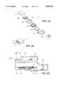
- FIG. 2Ais a diagrammatic perspective view of she main parts of an embodiment of an integrated microphone/amplifier unit according to the invention, in dismounted condition;
- FIG. 2Bis a diagrammatic perspective view of the integrated microphone/amplifier unit of FIG. 2A in mounted condition;
- FIG. 2Cis a diagrammatic view of the integrated microphone/amplifier unit of FIG. 2A in mounted condition
- FIG. 3is a diagrammatic top view of a known amplifier module to illustrate the layout thereof;
- FIGS. 4A-Cillustrate the layout of an amplifier module according to the present invention
- FIG. 4Dis a diagrammatic cross-section taken along the line D--D in FIG. 4C;
- FIG. 5Ais a view comparable to FIG. 4A of a layout of the variant shown in FIG. 1B;
- FIG. 5Bis a view of the layout of the variant of the invention and comparable to FIG. 4C;
- FIGS. 6A-Cdiagrammatically illustrate the layout of another embodiment of the invention, in which FIG. 6A is a top view and FIGS. 6B-C are bottom views.
- the inventionis particularly, but not exclusively, useful in a hearing aid and will therefore be described below in the context of such a practical example.
- the microphone/amplifier unit 1which is also briefly referred to as microphone, comprises a box-shaped housing 10 and a cover 11, a sound inlet nozzle 12, a backplate 13 provided with a charged electret layer, a membrane 14, a fastening plate 15, and an amplifier module 100.
- the combination of backplate 13 and membrane 14is referred to as microphone capsule 2.
- the backplate 13 with the membrane 14is mounted near the bottom of the horsing 10
- the fastening plate 15is mounted on the housing 10
- the amplifier module 100is mounted on the fastening plate 15.
- the cover 11is placed over the module 100, with the electric connections 5, 6, 7 of the module 100 being left clear. Sound can reach the interior of the housing 10 via the sound inlet nozzle 12, thus causing the membrane 14 to move so that the electret-microphone capsule 2 generates an electric capsule signal.
- the electret-microphone capsule 2is connected by means of connecting wires 17, which extend through a passage opening 16 in the fastening plate 15, with input connecting points 3 and 4 of the amplifier module 100 forming part of the unit 1, to supply the capsule signal thereto.
- the electric connecting points 5, 6, 7comprise two connections 5, 7 for supplying electric power to the module 100, and a signal output connecting point 6 for supplying an amplifier output signal, also referred to as microphone signal.
- One of the feed connecting points 7is connected with one of the input connecting points 4; this feed connecting point 7 will also be referred to as ground connection.
- the other feed connecting point 5will also be referred to as feed input.
- the feed input 5is usually positive with respect to the ground connection 7.
- the amplifier module 100comprises an amplifier 110, which, in the case shown, is a source-follower connected FET.
- the amplifier 110has an input 111, which is connected with the microphone input 3, and which is connected with the ground connection 7 via a first resistor R1.
- a feed input 112 of the amplifier 110is connected with the feed input 5, while an output 113 of the amplifier 110 is connected with the ground connection 7 via a second resistor R2, and is further connected with the output connection 6.
- a first capacitive coupling 8is present between the output connection 6 and the ground connection 7, and furthermore, a second capacitive coupling 9 is present between the feed input 5 and the ground connection 7.
- the capacity values of the two capacitive couplings 8 and 9are about 30 pF in a suitable embodiment. To optimize the suppression at specific frequencies, however, another value may be selected for the above capacity, if desired.
- the capacitive couplings 8, 9preferably form part of the amplifier module 100 because it is then possible to have the amplifier module 100 itself provide an interference suppressed microphone signal at its output 6. Furthermore, it is then possible, as will be explained below in more detail, to design the amplifier module 100 in a manner such that, including the capacitive couplings 8, 9, it is exchangeable with existing modules that lack such a feature.
- FIG. 1Billustrates a variant 100' of the amplifier module 100 illustrated in FIG. 1A, in which an additional ground connection 7' is present besides the ground connection 7.
- the capacitive couplings 8, 9are then realized with respect to this additional ground connection 7'; apart from that, the amplifier module 100' is identical to the amplifier module 100 of FIG. 1A.
- the advantage of an additional ground connection 7'is that the ground connection for the high-frequency interference signals is thereby separated from the ground connection for the low-frequency microphone signals so that the sensitivity of the unit 1 to high-frequency interference signals is further decreased.
- the high-frequency ground connection 7'is connected with the conducting housing 10, 11 of the unit 1, but, for the sake of simplicity, this is not illustrated.
- the low-frequency ground connection 7can then be coupled with the high-frequency ground connection 7' via an inductor (not shown).
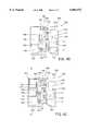
- the module 99comprises a plate-shaped carrier 120 of an electrically insulating material, such as A1 2 O 3 , having a thickness of about 0.254 mm.
- the carrier 120is substantially square and has four edges 121, 122, 123, 124, each having a length of about 2.8 mm.
- Applied to the carrier 120is a pattern of a conducting material, such as copper or, preferably, an AgPd alloy having a thickness of about 10-14 ⁇ m. This pattern comprises a first island 131 for fastening the amplifier 110.
- contact surfaces 132, 133 and 134Arranged on the carrier 120 near the first island 131 are contact surfaces 132, 133 and 134, with which the amplifier 110 can be connected by means of wire bonding. These contact surfaces 132, 133, 134 are made of gold having a thickness of about 10-12 ⁇ m.
- the pattern of conducting materialfurther comprises five islands defining the microphone connecting points 3, 4, the feed input 5, the ground connection 7 and the signal output connection 6.
- the feed input 5, the signal output connection 6 and the ground connection 7are arranged, gram above to below in FIG. 3, along the first edge 121 of the carrier 120.
- the amplifier island 131 and the microphone connecting points 3, 4are arranged, from above to below in FIG. 3, along the third edge 123, opposite the first edge 121.
- the patternfurther comprises some conducting connecting strips, as follows.
- a first connecting strip 141connects the microphone connecting point 4 with the ground connection 7.
- a second connecting strip 142connects the other microphone connecting point 3 with the amplifier island 131.
- a third connecting strip 143connects the first golden contact surface 132 with the feed input 5.
- the first connecting strip 141Arranged transversely to the first connecting strip 141 are two resistor surfaces 161 and 162 which define respectively the resistors R and R2.
- the first resistor surface 161is connected by a fourth connecting strip 144 with the third golden contact surface 134.
- the second resistor surface 162is connected by a fifth connecting strip 145 with the second golden contact surface 133.
- This fifth connecting strip 145is connected by a sixth connecting strip 146 with the signal output connection 6.
- the present inventionsolves this problem by providing a conducting base surface below each of the connecting surfaces 5 and 6, with interposition of dielectric intermediate layers between these connecting surfaces 5 and 6, the conducting base surfaces being connected with a ground connection.
- the connecting surfaces 5 and 6themselves then form, together with the conducting base surfaces a capacitor.
- the conducting base surfacesare integrally formed; the same applies to the dielectric intermediate layers.
- FIG. 4Ashows the base pattern of an embodiment of the module 100 according to the present invention.
- a comparison with FIG. 3will show that the connecting surfaces 5, 6 and 7 are replaced by a single conducting base surface 151, extending along the first edge 121 of the carrier 120, which base surface is connected with the first connecting strip 141.
- the sixth connecting strip 146is absent, and the third connecting strip 143 is replaced by a short connecting strip 147, which is only connected with the first golden contact surface 132.
- FIG. 4Bshows that an insulating dielectric layer 152 is applied over a part of the base surface 151.
- FIG. 4Cshow that, subsequently, a second pattern of conducting material, e.g. copper, but preferably AgPd, having a thickness of 10-14 ⁇ m, is applied over the dielectric layer 152.
- This second patterncomprises a first surface 153, which is connected via a connecting strip 154 with the short connecting strip 147, and a second surface 155, which is connected via a connecting strip 156 with the fifth connecting strip 145.
- the surfaces 153 and 155correspond to the connecting points 5 and 6, while, as regards position and function, the part 157 of the conducting surface 151 not covered by the dielectric 152 corresponds to the ground connection 7.
- each of the surfaces 153 and 155is capacitively coupled with the conducting surface 151, and thus with the surface part 157, and the capacity value may be about 30 pF by a suitable selection of type and thickness of the dielectric.
- each surface 153, 155is about 0.7 ⁇ 0.7 mm
- the dielectrichas a thickness of about 40 ⁇ m and the dielectric preferably has an ⁇ -value greater than 200.
- a suitable dielectric materialis commercially sold by DuPont, e.g. under the type designation 8229S. Applying the dielectric to the base surface 151 and applying a second pattern of conducting material over the dielectric layer 152 can be done by known per se processes, as will be clear to a skilled worker.
- the dielectricforms a continuous layer, that is to say without interruptions, because such interruptions are equivalent to a short circuit between the surfaces 153, 155 and 151.
- an insulating frame 158e.g. of glass, can be arranged over the carrier 120, with openings in the frame being aligned with the connecting surfaces 153, 155 and 157.
- the openings in the framecan be filled with solder 159, e.g. 62Sn/36Pb/2Ag. This is illustrated in the cross-section of FIG. 4D. It is clear therefrom that the appearance of the connecting points 5, 6 and 7 is unchanged when compared with the known module 99, but that the capacitive couplings 8 and 9 are provided notwithstanding, without requiring space.
- an amplifier 110is arranged on the carrier 120, e.g. a JFET of the type J2N4338, the connecting points of which are connected with the connecting surfaces 132, 133, 134, e.g. by wire bonds, after which the whole of the FET and the wire bonds is encapsulated for protection purposes in, e.g., a resin. Since these steps do not form part of the present invention, while for these steps use can also be made of known per se processes already used in the manufacture of the known module 99, they are not discussed or illustrated in more detail.
- the amplifier 110is a buffer amplifier; it is also possible, however, that the amplifier effects amplification of the signal. Also, the amplifier 110 may be an IC.
- the conducting surface 151there is arranged on the conducting surface 151 one single dielectric layer 152, which extends below both surfaces 153 and 155. This is preferred, but, in principle, it is also possible to arrange a separate dielectric layer below each surface 153, 155.
- FIG. 5Ashows the base pattern of a variant 100' of the amplifier .nodule, which is based on the schematic diagram of FIG. 1B.
- the same or comparable parts as in FIGS. 3 and 4A-Dare indicated by the same reference numerals.
- a comparison with FIG. 3will show that the connecting surfaces 5 and 6 are replaced by a single conducting surface 171, which, unlike FIG. 4B, has no electric connection with the connecting surface 7.
- the surfaces 4, 3 and 131are slightly diminished and/or moved in the direction of the second edge 122 to make room for a HF ground connecting surface 7', which is connected with the surface 171 via a connecting strip 172 extending along the fourth edge 124.
- FIG. 5Athere is arranged, as shown in FIG. 5A, over the surface 171 a dielectric layer 152, with the conducting surfaces 153, 155 over it, which are connected via conducting strips 154 and 156 with respectively the connecting strips 147 and 145.
- planar connecting pointsare formed on the module 100.
- a planar connecting pointcan be suitably used, as has been described, as a plate of a capacitor to be integrated on the module.
- back of the carrierfor the construction of capacitors, as will now be described, with reference to FIGS. 6A-6C, for a carrier 220 of a configuration different from the configuration of the carrier 120 described, but the electric diagram of which is equal to the diagram already described.
- the carrier 220is not provided with connecting surfaces formed on the carrier 220, but with connecting pins 203, 204, 205, 206, 207 fastened to the carrier 220, which, in the example to be described, run parallel to the plane of the carrier.
- Such an embodiment of the amplifier moduleis known, and here, too, there is a wish to provide this module with interference suppressing capacities with retention of the shape and sizes of the module, and with retention of the positions of the connecting pins.
- FIG. 6Ashows an elongate carrier 220 having sizes of about 5 mm by about 1.6 mm.
- the same reference numerals as in FIG. 3indicate the same or comparable parts.
- the first connecting strip 141is located at a first end of the carrier 220 and extends over substantially the entire width of the carrier 220. Soldered to this first connecting strip 141 are two pins 204 and 207, which extend beyond the edges of the carrier 220, to define the connecting points 4 and 7.
- the two pins 204 and 207may also be formed by a single continuous pin.
- the third connecting strip 143is located at the other end of the carrier 220 and extends over substantially the entire width of the carrier 220. Soldered to this third connecting strip 143 is a pin 205, which extends beyond the edge of the carrier 220 on the same side as the earlier mentioned pin 207, to define the connecting point 5. Between the pins 205 and 207 a pin 206 is soldered to the fifth connecting strip 145, to define the connecting point 6. On the opposite side a pin 203 is soldered to the second connecting strip 142, to define the connecting point 3. The pins may also be attached in a different manner, but soldering is preferred. It is observed that in this embodiment the third golden contact island 134 is omitted because the second connecting strip 142 also effects the connection between the surface 131 and the first resistor 161.
- the parts discussed with reference to FIG. 6Aare located on a first main surface of the carrier 220 and may be identical to the parts of an already known module as regards type and position.
- FIG. 6Bshows that on an other main surface (opposite to that shown in FIG. 6A) of the carrier 220, too, there is arranged a pattern of a conducting layer.
- This patterncomprises two substantially square base surfaces 231 and 232, which are connected together by means of a connecting strip 233.
- a connecting strip 233Provided in the carrier 220 are three holes 234, 235 and 236, respectively at the height of the third connecting strip 143, the fifth connecting strip 145 and the first connecting strip 141.
- the pattern on the other main surface of the carrier 220further comprises three contact surfaces 237, 238 and 239, which extend around respectively the holes 234, 235 and 236, and which are electrically connected through these holes with respectively the third connecting strip 143, the fifth connecting strip 145 and the first connecting strip 141, e.g. by bushings (not shown) introduced into the holes and secured on both sides by soldering.
- the third contact surface 238is connected with the surface 232 so that both base surfaces 231 and 232 are electrically connected
- the two base surfaces 231 and 232perform the same function as the base surface 151 discussed with reference to FIG. 4A.
- FIG. 6Cshows that over the two base surfaces 231 and 232 there are arranged dielectric layers, respectively 241 and 242, which together perform the same function as the base surface 152 discussed with reference to FIG. 4B.
- conducting surfacesrespectively 243 and 244, which are connected by means of connecting strips, respectively 245 and 246, with the contact surfaces 237 and 238.
- the conducting surface 243is electrically connected with the connecting point 5
- the conducting surface 244is electrically connected with the connecting point 6.
- the conducting surface 243 and the base surface 231 with the interposed dielectric layer 241define a capacitor which defines the capacitive coupling 9
- the conducting surface 244 and the base surface 232 with the interposed dielectric layer 242define a capacitor which defines the capacitive coupling 8 (capacitive couplings 8 and 9 being schematically shown in FIGS. 1A and 1B).
- a protective layere.g. of glass.
Landscapes
- Physics & Mathematics (AREA)
- Engineering & Computer Science (AREA)
- Acoustics & Sound (AREA)
- Signal Processing (AREA)
- Electrostatic, Electromagnetic, Magneto- Strictive, And Variable-Resistance Transducers (AREA)
- Amplifiers (AREA)
- Details Of Audible-Bandwidth Transducers (AREA)
Abstract
Description
Claims (22)
Applications Claiming Priority (2)
| Application Number | Priority Date | Filing Date | Title |
|---|---|---|---|
| NL1002783ANL1002783C2 (en) | 1996-04-03 | 1996-04-03 | Integrated microphone / amplifier unit, and amplifier module therefor. |
| NL1002783 | 1996-04-03 |
Publications (1)
| Publication Number | Publication Date |
|---|---|
| US6084972Atrue US6084972A (en) | 2000-07-04 |
Family
ID=19762615
Family Applications (1)
| Application Number | Title | Priority Date | Filing Date |
|---|---|---|---|
| US08/832,136Expired - LifetimeUS6084972A (en) | 1996-04-03 | 1997-04-03 | Integrated microphone/amplifier unit, and amplifier module therefor |
Country Status (6)
| Country | Link |
|---|---|
| US (1) | US6084972A (en) |
| EP (1) | EP0800331B1 (en) |
| AT (1) | ATE234540T1 (en) |
| DE (1) | DE69719585T2 (en) |
| DK (1) | DK0800331T3 (en) |
| NL (1) | NL1002783C2 (en) |
Cited By (21)
| Publication number | Priority date | Publication date | Assignee | Title |
|---|---|---|---|---|
| WO2001078446A1 (en)* | 2000-04-07 | 2001-10-18 | Microtronic Nederland B.V. | Microphone with range switching |
| US20010043705A1 (en)* | 2000-05-17 | 2001-11-22 | Engbert Wilmink | System consisting of a microphone and an amplifier |
| US20020034312A1 (en)* | 2000-06-08 | 2002-03-21 | Matsushita Electric Industrial Co., Ltd. | Capacitor microphone |
| US20030063768A1 (en)* | 2001-09-28 | 2003-04-03 | Cornelius Elrick Lennaert | Microphone for a hearing aid or listening device with improved dampening of peak frequency response |
| WO2003086014A1 (en)* | 2002-04-11 | 2003-10-16 | Rion Co.,Ltd | Impedance converter for capacitor microphone |
| US20030208362A1 (en)* | 2002-05-03 | 2003-11-06 | Resident Data, Inc. | Integrated screening system and method for tenants and rental applicants |
| US20040252858A1 (en)* | 2003-04-28 | 2004-12-16 | Boor Steven E. | Method and apparatus for substantially improving power supply rejection performance in a miniature microphone assembly |
| US6851048B2 (en) | 1997-01-13 | 2005-02-01 | Micro Ear Technology, Inc. | System for programming hearing aids |
| US6888948B2 (en) | 1997-01-13 | 2005-05-03 | Micro Ear Technology, Inc. | Portable system programming hearing aids |
| US6895345B2 (en) | 1998-01-09 | 2005-05-17 | Micro Ear Technology, Inc. | Portable hearing-related analysis system |
| US6914992B1 (en)* | 1998-07-02 | 2005-07-05 | Sonion Nederland B.V. | System consisting of a microphone and a preamplifier |
| US20050185807A1 (en)* | 2004-02-25 | 2005-08-25 | Kabushiki Kaisha Audio-Technica | Condenser microphone |
| US20050213787A1 (en)* | 2004-03-26 | 2005-09-29 | Knowles Electronics, Llc | Microphone assembly with preamplifier and manufacturing method thereof |
| US20060008105A1 (en)* | 2004-07-09 | 2006-01-12 | Knowles Electronics, Llc | Apparatus for suppressing radio frequency interference in a microphone assembly with preamplifier |
| US7039202B1 (en)* | 2000-02-15 | 2006-05-02 | Mitsubishi Denki Kabushiki Kaisha | Microphone unit |
| US7072482B2 (en) | 2002-09-06 | 2006-07-04 | Sonion Nederland B.V. | Microphone with improved sound inlet port |
| US20090232335A1 (en)* | 2008-03-13 | 2009-09-17 | Kabushiki Kaisha Audio-Technica | Condenser microphone |
| US7787647B2 (en) | 1997-01-13 | 2010-08-31 | Micro Ear Technology, Inc. | Portable system for programming hearing aids |
| US20110228954A1 (en)* | 2010-03-17 | 2011-09-22 | Martins Saulespurens | Electret Microphone Circuit |
| US8300862B2 (en) | 2006-09-18 | 2012-10-30 | Starkey Kaboratories, Inc | Wireless interface for programming hearing assistance devices |
| US8503703B2 (en) | 2000-01-20 | 2013-08-06 | Starkey Laboratories, Inc. | Hearing aid systems |
Families Citing this family (9)
| Publication number | Priority date | Publication date | Assignee | Title |
|---|---|---|---|---|
| EP0835041A1 (en)* | 1996-10-02 | 1998-04-08 | Siemens Audiologische Technik GmbH | Electric hearing aid with protection device against electromagnetic radiation |
| WO2000010363A1 (en)* | 1998-08-13 | 2000-02-24 | Siemens Audiologische Technik Gmbh | Hearing aid comprising a device for suppressing electromagnetic interference signals and method for suppressing electromagnetic interference signals in hearing aids |
| EP1142442A2 (en) | 1999-01-07 | 2001-10-10 | Sarnoff Corporation | Hearing aid with large diaphragm microphone element including a printed circuit board |
| US7003127B1 (en) | 1999-01-07 | 2006-02-21 | Sarnoff Corporation | Hearing aid with large diaphragm microphone element including a printed circuit board |
| DE60011349T2 (en) | 1999-07-08 | 2005-06-16 | Matsushita Electric Industrial Co., Ltd., Kadoma | Condenser Microphone Device and Connecting Device |
| WO2001050814A1 (en)* | 2000-01-06 | 2001-07-12 | Sarnoff Corporation | Microphone assembly with jfet flip-chip buffer for hearing aid |
| JP4129108B2 (en)* | 2000-02-25 | 2008-08-06 | 三菱電機株式会社 | Microphone filter and microphone device |
| US7415121B2 (en) | 2004-10-29 | 2008-08-19 | Sonion Nederland B.V. | Microphone with internal damping |
| WO2025040675A1 (en)* | 2023-08-21 | 2025-02-27 | Widex A/S | Method of operating a hearing aid and hearing aid |
Citations (8)
| Publication number | Priority date | Publication date | Assignee | Title |
|---|---|---|---|---|
| US3270146A (en)* | 1963-03-14 | 1966-08-30 | Motorola Inc | Hearing aid |
| US4280018A (en)* | 1979-05-14 | 1981-07-21 | Strobotronix, Inc. | Integrated piezoelectric sound transducer and preamplifier |
| US4516428A (en)* | 1982-10-28 | 1985-05-14 | Pan Communications, Inc. | Acceleration vibration detector |
| DE3425175A1 (en)* | 1984-07-09 | 1986-03-27 | Fernsprech- und Signalbau KG Schüler & Vershoven, 4300 Essen | Piezoelectric acoustic transducer |
| US4888807A (en)* | 1989-01-18 | 1989-12-19 | Audio-Technica U.S., Inc. | Variable pattern microphone system |
| US4993072A (en)* | 1989-02-24 | 1991-02-12 | Lectret S.A. | Shielded electret transducer and method of making the same |
| WO1994014239A1 (en)* | 1992-12-14 | 1994-06-23 | Knowles Electronics, Inc. | Pre-amplifier |
| EP0670602A1 (en)* | 1994-02-28 | 1995-09-06 | Nec Corporation | Field effect transistor having capacitor between source and drain electrodes |
Family Cites Families (1)
| Publication number | Priority date | Publication date | Assignee | Title |
|---|---|---|---|---|
| FR2669802B1 (en)* | 1990-11-23 | 1993-06-18 | Intrason France | ELECTRONIC DEVICE FORMING MINIATURE PROGRAMMABLE HEARING AID, PARTICULARLY OF THE INTRA-DUCT TYPE. |
- 1996
- 1996-04-03NLNL1002783Apatent/NL1002783C2/ennot_activeIP Right Cessation
- 1997
- 1997-04-02DKDK97200968Tpatent/DK0800331T3/enactive
- 1997-04-02DEDE69719585Tpatent/DE69719585T2/ennot_activeExpired - Lifetime
- 1997-04-02EPEP97200968Apatent/EP0800331B1/ennot_activeExpired - Lifetime
- 1997-04-02ATAT97200968Tpatent/ATE234540T1/ennot_activeIP Right Cessation
- 1997-04-03USUS08/832,136patent/US6084972A/ennot_activeExpired - Lifetime
Patent Citations (9)
| Publication number | Priority date | Publication date | Assignee | Title |
|---|---|---|---|---|
| US3270146A (en)* | 1963-03-14 | 1966-08-30 | Motorola Inc | Hearing aid |
| US4280018A (en)* | 1979-05-14 | 1981-07-21 | Strobotronix, Inc. | Integrated piezoelectric sound transducer and preamplifier |
| US4516428A (en)* | 1982-10-28 | 1985-05-14 | Pan Communications, Inc. | Acceleration vibration detector |
| DE3425175A1 (en)* | 1984-07-09 | 1986-03-27 | Fernsprech- und Signalbau KG Schüler & Vershoven, 4300 Essen | Piezoelectric acoustic transducer |
| US4888807A (en)* | 1989-01-18 | 1989-12-19 | Audio-Technica U.S., Inc. | Variable pattern microphone system |
| US4993072A (en)* | 1989-02-24 | 1991-02-12 | Lectret S.A. | Shielded electret transducer and method of making the same |
| WO1994014239A1 (en)* | 1992-12-14 | 1994-06-23 | Knowles Electronics, Inc. | Pre-amplifier |
| US5337011A (en)* | 1992-12-14 | 1994-08-09 | Knowles Electronics, Inc. | Pre-amplifier |
| EP0670602A1 (en)* | 1994-02-28 | 1995-09-06 | Nec Corporation | Field effect transistor having capacitor between source and drain electrodes |
Cited By (34)
| Publication number | Priority date | Publication date | Assignee | Title |
|---|---|---|---|---|
| US7929723B2 (en) | 1997-01-13 | 2011-04-19 | Micro Ear Technology, Inc. | Portable system for programming hearing aids |
| US7451256B2 (en) | 1997-01-13 | 2008-11-11 | Micro Ear Technology, Inc. | Portable system for programming hearing aids |
| US7787647B2 (en) | 1997-01-13 | 2010-08-31 | Micro Ear Technology, Inc. | Portable system for programming hearing aids |
| US6888948B2 (en) | 1997-01-13 | 2005-05-03 | Micro Ear Technology, Inc. | Portable system programming hearing aids |
| US6851048B2 (en) | 1997-01-13 | 2005-02-01 | Micro Ear Technology, Inc. | System for programming hearing aids |
| US6895345B2 (en) | 1998-01-09 | 2005-05-17 | Micro Ear Technology, Inc. | Portable hearing-related analysis system |
| US6914992B1 (en)* | 1998-07-02 | 2005-07-05 | Sonion Nederland B.V. | System consisting of a microphone and a preamplifier |
| US8503703B2 (en) | 2000-01-20 | 2013-08-06 | Starkey Laboratories, Inc. | Hearing aid systems |
| US9344817B2 (en) | 2000-01-20 | 2016-05-17 | Starkey Laboratories, Inc. | Hearing aid systems |
| US9357317B2 (en) | 2000-01-20 | 2016-05-31 | Starkey Laboratories, Inc. | Hearing aid systems |
| US7039202B1 (en)* | 2000-02-15 | 2006-05-02 | Mitsubishi Denki Kabushiki Kaisha | Microphone unit |
| WO2001078446A1 (en)* | 2000-04-07 | 2001-10-18 | Microtronic Nederland B.V. | Microphone with range switching |
| US6950529B2 (en)* | 2000-05-17 | 2005-09-27 | Sonionmicrotronic Nederland B.V. | System consisting of a microphone and an amplifier |
| US20010043705A1 (en)* | 2000-05-17 | 2001-11-22 | Engbert Wilmink | System consisting of a microphone and an amplifier |
| US20020034312A1 (en)* | 2000-06-08 | 2002-03-21 | Matsushita Electric Industrial Co., Ltd. | Capacitor microphone |
| US7065224B2 (en)* | 2001-09-28 | 2006-06-20 | Sonionmicrotronic Nederland B.V. | Microphone for a hearing aid or listening device with improved internal damping and foreign material protection |
| US20030063768A1 (en)* | 2001-09-28 | 2003-04-03 | Cornelius Elrick Lennaert | Microphone for a hearing aid or listening device with improved dampening of peak frequency response |
| WO2003086014A1 (en)* | 2002-04-11 | 2003-10-16 | Rion Co.,Ltd | Impedance converter for capacitor microphone |
| US20030208362A1 (en)* | 2002-05-03 | 2003-11-06 | Resident Data, Inc. | Integrated screening system and method for tenants and rental applicants |
| US7072482B2 (en) | 2002-09-06 | 2006-07-04 | Sonion Nederland B.V. | Microphone with improved sound inlet port |
| US20040252858A1 (en)* | 2003-04-28 | 2004-12-16 | Boor Steven E. | Method and apparatus for substantially improving power supply rejection performance in a miniature microphone assembly |
| US7352876B2 (en) | 2003-04-28 | 2008-04-01 | Knowles Electronics, Llc. | Method and apparatus for substantially improving power supply rejection performance in a miniature microphone assembly |
| US7382889B2 (en)* | 2004-02-25 | 2008-06-03 | Kabushiki Kaisha Audio-Technica | Condenser microphone |
| US20050185807A1 (en)* | 2004-02-25 | 2005-08-25 | Kabushiki Kaisha Audio-Technica | Condenser microphone |
| US20070286445A1 (en)* | 2004-03-26 | 2007-12-13 | Knowles Electronics, Llc | Microphone Assembly with Preamplifier and Manufacturing Method Thereof |
| US20050213787A1 (en)* | 2004-03-26 | 2005-09-29 | Knowles Electronics, Llc | Microphone assembly with preamplifier and manufacturing method thereof |
| US7706559B2 (en)* | 2004-07-09 | 2010-04-27 | Knowles Electronics, Llc | Apparatus for suppressing radio frequency interference in a microphone assembly with preamplifier |
| US20060008105A1 (en)* | 2004-07-09 | 2006-01-12 | Knowles Electronics, Llc | Apparatus for suppressing radio frequency interference in a microphone assembly with preamplifier |
| US8300862B2 (en) | 2006-09-18 | 2012-10-30 | Starkey Kaboratories, Inc | Wireless interface for programming hearing assistance devices |
| US8126165B2 (en) | 2008-03-13 | 2012-02-28 | Kabushiki Kaisha Audio-Technica | Condenser microphone |
| JP2009224839A (en)* | 2008-03-13 | 2009-10-01 | Audio Technica Corp | Condenser microphone |
| US20090232335A1 (en)* | 2008-03-13 | 2009-09-17 | Kabushiki Kaisha Audio-Technica | Condenser microphone |
| US20110228954A1 (en)* | 2010-03-17 | 2011-09-22 | Martins Saulespurens | Electret Microphone Circuit |
| US8588433B2 (en) | 2010-03-17 | 2013-11-19 | Baltic Latvian Universal Electronics, Llc | Electret microphone circuit |
Also Published As
| Publication number | Publication date |
|---|---|
| DK0800331T3 (en) | 2003-07-14 |
| EP0800331A3 (en) | 1998-01-14 |
| DE69719585T2 (en) | 2004-01-08 |
| NL1002783C2 (en) | 1997-10-06 |
| EP0800331B1 (en) | 2003-03-12 |
| ATE234540T1 (en) | 2003-03-15 |
| DE69719585D1 (en) | 2003-04-17 |
| EP0800331A2 (en) | 1997-10-08 |
Similar Documents
| Publication | Publication Date | Title |
|---|---|---|
| US6084972A (en) | Integrated microphone/amplifier unit, and amplifier module therefor | |
| US6324907B1 (en) | Flexible substrate transducer assembly | |
| CN102740205B (en) | Packaging and method for packaging a microphone device | |
| EP1303164B1 (en) | Microphone having a flexible printed circuit board for mounting components | |
| EP2352311B1 (en) | Microphone | |
| CN111050259B (en) | Microphone packaging structure and electronic device | |
| US20020090102A1 (en) | Microphone assembly for hearing aid with JFET flip-chip buffer | |
| CN101507376B (en) | sound output device | |
| CN101296531B (en) | Silicon capacitor microphone array | |
| US7352876B2 (en) | Method and apparatus for substantially improving power supply rejection performance in a miniature microphone assembly | |
| JP2011114506A (en) | Microphone unit | |
| CN110856090A (en) | Novel anti-radio frequency interference micro-electro-mechanical system microphone structure | |
| US6950529B2 (en) | System consisting of a microphone and an amplifier | |
| JP3479464B2 (en) | Unidirectional electret condenser microphone | |
| US4286122A (en) | Acoustic electrical conversion device with at least one capacitor electret element connected to an electronic circuit | |
| KR100919939B1 (en) | Small-sized capacitor micro-phone | |
| WO2005022950A1 (en) | Speaker device | |
| KR200438928Y1 (en) | Dual microphone module | |
| CN211089969U (en) | Microphone packaging structure and electronic equipment | |
| CN109348385A (en) | A kind of microphone and electronic equipment with echo sound-attenuating system | |
| WO1996037086A1 (en) | Hf-anti-interference device | |
| CN210603698U (en) | Capacitive air pressure sensor and electronic equipment | |
| CN219287719U (en) | Combined sensor with radio and sound producing function | |
| JP3158850B2 (en) | microphone | |
| CN210016616U (en) | A speaker with in-ear detection function |
Legal Events
| Date | Code | Title | Description |
|---|---|---|---|
| AS | Assignment | Owner name:MICROTRONIC NEDERLAND B.V., NETHERLANDS Free format text:ASSIGNMENT OF ASSIGNORS INTEREST;ASSIGNORS:VAN HALTEREN, AART Z.;WILMINK, ENGBERT;REEL/FRAME:008689/0340 Effective date:19970602 | |
| STCF | Information on status: patent grant | Free format text:PATENTED CASE | |
| AS | Assignment | Owner name:SONIONMICROTRONIC NEDERLAND B.V., NETHERLANDS Free format text:ASSIGNMENT OF ASSIGNORS INTEREST;ASSIGNOR:MICROTRONIC NEDERLAND B.V.;REEL/FRAME:013828/0972 Effective date:20030225 | |
| FEPP | Fee payment procedure | Free format text:PAT HOLDER NO LONGER CLAIMS SMALL ENTITY STATUS, ENTITY STATUS SET TO UNDISCOUNTED (ORIGINAL EVENT CODE: STOL); ENTITY STATUS OF PATENT OWNER: LARGE ENTITY | |
| REFU | Refund | Free format text:REFUND - SURCHARGE, PETITION TO ACCEPT PYMT AFTER EXP, UNINTENTIONAL (ORIGINAL EVENT CODE: R2551); ENTITY STATUS OF PATENT OWNER: LARGE ENTITY | |
| FPAY | Fee payment | Year of fee payment:4 | |
| FPAY | Fee payment | Year of fee payment:8 | |
| FEPP | Fee payment procedure | Free format text:PAYOR NUMBER ASSIGNED (ORIGINAL EVENT CODE: ASPN); ENTITY STATUS OF PATENT OWNER: LARGE ENTITY | |
| AS | Assignment | Owner name:SONION NEDERLAND B.V., NETHERLANDS Free format text:CHANGE OF NAME;ASSIGNOR:SONIONMICROTRONIC NEDERLAND B.V.;REEL/FRAME:023134/0538 Effective date:20090804 | |
| AS | Assignment | Owner name:PULSE NEDERLAND B.V., NETHERLANDS Free format text:MERGER;ASSIGNOR:SONION NEDERLAND B.V.;REEL/FRAME:023312/0944 Effective date:20090804 Owner name:PULSE NEDERLAND B.V.,NETHERLANDS Free format text:MERGER;ASSIGNOR:SONION NEDERLAND B.V.;REEL/FRAME:023312/0944 Effective date:20090804 | |
| AS | Assignment | Owner name:SONION NEDERLAND B.V.,NETHERLANDS Free format text:ASSIGNMENT OF ASSIGNORS INTEREST;ASSIGNOR:PULSE NEDERLAND B.V.;REEL/FRAME:024120/0332 Effective date:20091112 Owner name:SONION NEDERLAND B.V., NETHERLANDS Free format text:ASSIGNMENT OF ASSIGNORS INTEREST;ASSIGNOR:PULSE NEDERLAND B.V.;REEL/FRAME:024120/0332 Effective date:20091112 | |
| FPAY | Fee payment | Year of fee payment:12 |