US6084459A - Voltage level shifting circuit - Google Patents
Voltage level shifting circuitDownload PDFInfo
- Publication number
- US6084459A US6084459AUS08/953,510US95351097AUS6084459AUS 6084459 AUS6084459 AUS 6084459AUS 95351097 AUS95351097 AUS 95351097AUS 6084459 AUS6084459 AUS 6084459A
- Authority
- US
- United States
- Prior art keywords
- voltage
- pull
- terminal
- pmos transistor
- transistor
- Prior art date
- Legal status (The legal status is an assumption and is not a legal conclusion. Google has not performed a legal analysis and makes no representation as to the accuracy of the status listed.)
- Expired - Lifetime
Links
Images

Classifications
- H—ELECTRICITY
- H03—ELECTRONIC CIRCUITRY
- H03K—PULSE TECHNIQUE
- H03K5/00—Manipulating of pulses not covered by one of the other main groups of this subclass
- H03K5/01—Shaping pulses
- H03K5/02—Shaping pulses by amplifying
- H—ELECTRICITY
- H03—ELECTRONIC CIRCUITRY
- H03K—PULSE TECHNIQUE
- H03K3/00—Circuits for generating electric pulses; Monostable, bistable or multistable circuits
- H03K3/02—Generators characterised by the type of circuit or by the means used for producing pulses
- H03K3/353—Generators characterised by the type of circuit or by the means used for producing pulses by the use, as active elements, of field-effect transistors with internal or external positive feedback
- H03K3/356—Bistable circuits
- H03K3/356104—Bistable circuits using complementary field-effect transistors
Definitions
- the present inventionrelates to a voltage level shifting circuit, and in particular to an improved voltage level shifting circuit which is capable of increasing a level shifting speed and reducing a current consumption and a layout area.
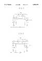
- the conventional voltage level shifting circuitincludes a PMOS transistor 10 and a first inverter 11 which are connected in series between a Vpp terminal and a Vss terminal, and a PMOS transistor 12 and a second inverter 13 which are connected in series between the Vpp terminal and Vss terminal and connected in parallel with the PMOS transistor 10 and the first inverter 11.
- the first inverter 11includes a pull-up PMOS transistor PM1 and a pull-down NMOS transistor NM1 the gate of each of which receives an input signal Vin, and the first voltage terminal V1 is connected with the gate of the PMOS transistor 12.
- the second inverter 13includes a pull-up PMOS transistor PM2 and a pull-down NMOS transistor NM2 the gate of each of which receives an inverted input signal Vin, and the second voltage terminal V2 is connected with the gate of the PMOS transistor 10.
- the pull-up PMOS transistor PMI of the first inverter 11 and the pull-down NMOS transistor NM2 of the second inverter 13are fully turned on, and the pull-up PMOS transistor PM2 of the second inverter 13 is slightly turned on.
- the driving capacity of the pull-down NMOS transistor NM2is increased to a predetermined level which is higher than the driving capacity of the pull-down PMOS transistor PM2, the second voltage terminal V2 of the second inverter 13 becomes a voltage Vss, and the first voltage terminal V1 of the first inverter 11 becomes a voltage Vpp.
- the final output voltage Voutbecomes a voltage Vss.
- the voltage at the first voltage terminal V1 of the first inverter 11becomes a voltage Vss, and the PMOS transistor 12 is turned on by the voltage Vss of the first inverter 11, whereby the voltage Vpp is applied to the second voltage terminal V2 of the second inverter 13.
- the PMOS transistor 10is turned off by the voltage Vpp of the second voltage terminal V2, so that the PMOS transistor 10 does not apply the power to the first voltage terminal V1.
- the voltage at the first voltage terminal V1 of the first inverter 11becomes a voltage Vss, and the PMOS transistor 12 is turned on by the voltage Vss, so that the output voltage Vout becomes a Vpp level.
- the conventional voltage level shifting circuitreceives a voltage Vdd and outputs a voltage Vpp (Vpp>Vdd).
- the size (W/L: Width/Length) of the PMOS transistorsshould be increased in order to obtain a sufficient driving capacity.
- a voltage level shifting circuitwhich includes a pull-up PMOS transistor and a pull-down NMOS transistor connected in series between a voltage Vpp terminal and a voltage Vss terminal and having a common drain which acts a first voltage terminal, a pull-up PMOS transistor and a pull-down NMOS transistor connected in series between the voltage Vpp terminal and the voltage Vss terminal, configured symmetrically with respect to the pull-up PMOS transistor and pull-down NMOS transistor, and having a common drain which acts as a second voltage terminal, a first conductive type MOS transistor a source of which is connected with a gate of the pull-up PMOS transistor and the second voltage terminal, respectively and a gate of which is connected with an input terminal, and a second conductive type MOS transistor a source of which is connected with a gate of the pull-up PMOS transistor and the first voltage terminal, respectively, and a gate of which is connected with the input terminal through an inverter.
- a voltage level shifting circuitwhich includes a NMOS transistor, a pull-up PMOS transistor, and a pull-down NMOS transistor connected in series between a voltage Vpp terminal and a voltage Vss terminal and having a common drain which acts as a first voltage terminal, a NMOS transistor, a pull-up PMOS transistor, and a pull-down NMOS transistor connected in series between the voltage Vpp terminal and the voltage Vss terminal and configured symmetrically with respect to the pull-up PMOS transistor and the pull-down NMOS transistor and having a common drain which acts as a second voltage terminal, a first conductive MOS transistor for increasing a level of the second voltage terminal during a level shifting and decreasing a driving capacity of the pull-up PMOS transistor, and a second conductive type MOS transistor for increasing a level of the first voltage terminal during a level shifting and decreasing a driving capacity of the pull-up PMOS transistor.
- a voltage level shifting circuitwhich includes a pull-up PMOS transistor, a PMOS transistor, and a pull-down NMOS transistor connected in series between a voltage Vpp terminal and a voltage Vss terminal and having a common drain which acts as a first voltage terminal, a pull-up PMOS transistor, a PMOS transistor, and a pull-down NMOS transistor connected in series between the voltage Vpp terminal and the voltage Vss terminal and configured symmetrically with respect to the pull-up PMOS transistor, the PMOS transistor, and the pull-down NMOS transistor and having a common train which acts as a second voltage terminal, a first conductive type MOS transistor for increasing a voltage level of the second voltage terminal during a level shifting and decreasing a driving capacity of the pull-up PMOS transistor, and a second conductive type MOS transistor for increasing a voltage level of the first voltage terminal during a level shifting and decreasing a driving capacity of the pull-up PMOS transistor.
- FIG. 1is a circuit diagram illustrating a conventional voltage level shifting circuit
- FIG. 2is a circuit diagram illustrating a voltage level shifting circuit according to a first embodiment of the present invention
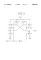
- FIG. 3is a circuit diagram illustrating a voltage level shifting circuit according to a second embodiment of the present invention.
- FIG. 4is a circuit diagram illustrating a voltage level shifting circuit according to a third embodiment of the present invention.
- FIG. 5is a circuit diagram illustrating a voltage level shifting circuit according to a fourth embodiment of the present invention.
- the voltage level shifting circuitincludes a pull-up PMOS transistor 20 and a pull-down NMOS transistor 21 which are connected in series between a voltage Vpp terminal and a voltage Vss terminal, a pull-up PMOS transistor 22 and a pull-down NMOS transistor 23 which are connected in series between a voltage Vpp terminal and a voltage Vss terminal and are symmetrical with respect to the connection of the pull-up PMOS transistor 20 and the pull-down NMOS transistor 21, an NMOS transistor 24, having a low threshold voltage Vthl, the source of which is connected with the gate of the pull-up PMOS transistor 20 and a second voltage terminal V2, respectively, and the gate of which is connected with an input terminal Vin, and an NMOS transistor 25, having a low threshold voltage Vthl, the source of which is connected with the gate of the pull-up PMOS transistor 22 and the first voltage terminal V1, respectively, the gate of which is connected with the input terminal Vin through an inverter.
- the NMOS transistor 25is turned on, and a voltage Vdd-Vthl at the source of the NMOS transistor 25 is applied to the gate of the pull-up PMOS transistor 22 and the first voltage terminal V1, respectively.
- the NMOS transistor 25increases the initial voltage of the first voltage terminal V1 and decreases the pull-up capacity of the pull-up PMOS transistor 22.
- the pull-up PMOS transistor 20is turned on by the voltage Vss of the second voltage terminal V2, the voltage is increased from "Vdd-Vthl" to Vpp at the first voltage terminal V1.
- the pull-up PMOS transistor 22is fully turned off by the voltage Vpp, and the second voltage terminal maintains the voltage Vss.
- the NMOS transistor 24 and the pull-down NMOS transistor 21are turned on, and the voltage Vdd-Vthl at the source of the NMOS transistor 24 is applied to the gate of the pull-up PMOS transistor 20 and the second voltage terminal V2, respectively.
- the NMOS transistor 24increases the initial voltage of the second voltage terminal V2 and decreases the pull-up capacity of the pull-up PMOS transistor 20.
- the pull-up PMOS transistor 22is turned on by the voltage Vss of the first voltage terminal V1, and the voltage at the second voltage terminal V2 and the gate voltage of the pull-up PMOS transistor 20 are increased from "Vdd-Vthl" to Vpp.
- the voltage at the second voltage terminal V2becomes the voltage Vpp and as the pull-up PMOS transistor 20 is fully turned off, the voltage at the first voltage terminal V1 becomes the voltage Vss.
- the pull-up capacity of the pull-up PMOS transistoris decreased by the NMOS transistor having a low threshold voltage, thus increasing a level shifting speed.
- the NMOS transistors 24 and 25 each having a low threshold voltage Vthl of the first embodiment of the present inventionare replaced with NMOS transistors 24' and 25' each having a common threshold voltage which is greater than the low threshold voltage Vthl.
- PMOS transistors 26 and 27are connected between the voltage Vpp terminal and the pull-up PMOS transistor 20 or the pull-up PMOS transistor 22.
- the pull-up capacities of the pull-up PMOS transistors 20 and 22are more increased by slightly turning on the PMOS transistors 26 and 27 in accordance with an externally applied signal for limiting a current flow, whereby a level shifting speed is increased and a current consumption is reduced.
- a PMOS transistor 28the gate of which is connected with the input terminal Vin, is connected between the pull-up PMOS transistor 20 and the pull-down NMOS transistor 21, and a PMOS transistor 29 the gate of which is connected with the input terminal Vin through the inverter, is connected between the pull-up PMOS transistor 22 and the pull-down NMOS transistor 23.
- the PMOS transistors 28 and 29are slightly turned on, thus limiting a current flow, so that in a side in which a voltage level is shifted to a low level, the current flow from the pull-up PMOS transistors 20 and 22 to the first and second voltage terminals V1 and V2, and in a side in which a voltage level is shifted to a high level, the pull-up capacity of the pull-up PMOS transistors 20 and 22 are decreased.
- the voltage level shiftingis performed by using one pull-up PMOS transistor, and in a side in which a voltage level is shifted to a low level, the pull-up capacity of the pull-up PMOS transistor is decreased by the NMOS transistor having a low threshold voltage or an externally applied signal, whereby the level shifting speed is increased and a current consumption is reduced.
Landscapes
- Physics & Mathematics (AREA)
- Nonlinear Science (AREA)
- Logic Circuits (AREA)
Abstract
Description
Claims (13)
Applications Claiming Priority (2)
| Application Number | Priority Date | Filing Date | Title |
|---|---|---|---|
| KR1019960058666AKR100218336B1 (en) | 1996-11-28 | 1996-11-28 | Level shifter |
| KR96/58666 | 1996-11-28 |
Publications (1)
| Publication Number | Publication Date |
|---|---|
| US6084459Atrue US6084459A (en) | 2000-07-04 |
Family
ID=19484098
Family Applications (1)
| Application Number | Title | Priority Date | Filing Date |
|---|---|---|---|
| US08/953,510Expired - LifetimeUS6084459A (en) | 1996-11-28 | 1997-10-17 | Voltage level shifting circuit |
Country Status (5)
| Country | Link |
|---|---|
| US (1) | US6084459A (en) |
| JP (1) | JPH10173511A (en) |
| KR (1) | KR100218336B1 (en) |
| DE (1) | DE19751789A1 (en) |
| TW (1) | TW417283B (en) |
Cited By (13)
| Publication number | Priority date | Publication date | Assignee | Title |
|---|---|---|---|---|
| US6369632B1 (en)* | 1999-08-25 | 2002-04-09 | Stmicroelectronics Limited | CMOS switching circuitry |
| US6563362B2 (en)* | 1999-11-23 | 2003-05-13 | Koninklijke Philips Electronics N.V. | Voltage translator circuit |
| US20050242669A1 (en)* | 2004-04-30 | 2005-11-03 | Fattaruso John W | Apparatus and method for shifting a signal from a first reference level to a second reference level |
| US20050258864A1 (en)* | 2004-05-24 | 2005-11-24 | Taiwan Semiconductor Manufacturing Company, Ltd. | Integrated circuit for level-shifting voltage levels |
| US20060220682A1 (en)* | 2005-03-29 | 2006-10-05 | Youichi Satou | Voltage level converter circuit and semiconductor integrated circuit device |
| US20060290379A1 (en)* | 2005-06-27 | 2006-12-28 | Rowley Matthew D | Leakage balancing transistor for jitter reduction in CML to CMOS converters |
| US20070146042A1 (en)* | 2005-12-28 | 2007-06-28 | Nec Corporation | Level shift circuit and driver circuit using the same |
| US20070229139A1 (en)* | 2006-03-30 | 2007-10-04 | Chun-Hung Lin | Level shifter circuit with a wide operating voltage range |
| US20080100341A1 (en)* | 2006-10-26 | 2008-05-01 | Min-Hwahn Kim | Level shifter having single voltage source |
| US8319540B2 (en) | 2010-07-01 | 2012-11-27 | Integrated Device Technology, Inc. | Apparatuses and methods for a voltage level shifting |
| US8384431B2 (en) | 2010-12-09 | 2013-02-26 | Integrated Device Technology, Inc. | Voltage level shifting apparatuses and methods |
| KR20150096721A (en)* | 2012-12-20 | 2015-08-25 | 퀄컴 인코포레이티드 | Sense amplifier including a level shifter |
| CN107528581A (en)* | 2017-09-26 | 2017-12-29 | 格科微电子(上海)有限公司 | Level shifting circuit |
Families Citing this family (4)
| Publication number | Priority date | Publication date | Assignee | Title |
|---|---|---|---|---|
| DE19951129A1 (en)* | 1999-10-23 | 2001-04-26 | Bosch Gmbh Robert | Circuit varying voltage level of digital signal from first to second level |
| JP2002176351A (en)* | 2000-12-06 | 2002-06-21 | Kawasaki Microelectronics Kk | Level shifter circuit |
| JP4087229B2 (en)* | 2002-03-11 | 2008-05-21 | 三菱電機株式会社 | Amplitude conversion circuit and semiconductor device using the same |
| KR100594319B1 (en) | 2005-02-02 | 2006-06-30 | 삼성전자주식회사 | Level Shifter with Extended Input Levels |
Citations (3)
| Publication number | Priority date | Publication date | Assignee | Title |
|---|---|---|---|---|
| US4695744A (en)* | 1985-12-16 | 1987-09-22 | Rca Corporation | Level shift circuit including source follower output |
| US4845381A (en)* | 1987-10-01 | 1989-07-04 | Vlsi Technology, Inc. | Voltage level shifting circuit |
| US5698993A (en)* | 1996-03-28 | 1997-12-16 | Industrial Technology Research Institute | CMOS level shifting circuit |
- 1996
- 1996-11-28KRKR1019960058666Apatent/KR100218336B1/ennot_activeExpired - Fee Related
- 1997
- 1997-10-17USUS08/953,510patent/US6084459A/ennot_activeExpired - Lifetime
- 1997-10-20TWTW086115444Apatent/TW417283B/ennot_activeIP Right Cessation
- 1997-11-21DEDE19751789Apatent/DE19751789A1/ennot_activeWithdrawn
- 1997-11-28JPJP9327280Apatent/JPH10173511A/enactivePending
Patent Citations (3)
| Publication number | Priority date | Publication date | Assignee | Title |
|---|---|---|---|---|
| US4695744A (en)* | 1985-12-16 | 1987-09-22 | Rca Corporation | Level shift circuit including source follower output |
| US4845381A (en)* | 1987-10-01 | 1989-07-04 | Vlsi Technology, Inc. | Voltage level shifting circuit |
| US5698993A (en)* | 1996-03-28 | 1997-12-16 | Industrial Technology Research Institute | CMOS level shifting circuit |
Cited By (21)
| Publication number | Priority date | Publication date | Assignee | Title |
|---|---|---|---|---|
| US6369632B1 (en)* | 1999-08-25 | 2002-04-09 | Stmicroelectronics Limited | CMOS switching circuitry |
| US6563362B2 (en)* | 1999-11-23 | 2003-05-13 | Koninklijke Philips Electronics N.V. | Voltage translator circuit |
| US20050242669A1 (en)* | 2004-04-30 | 2005-11-03 | Fattaruso John W | Apparatus and method for shifting a signal from a first reference level to a second reference level |
| US7535280B2 (en)* | 2004-04-30 | 2009-05-19 | Texas Instruments Incorporated | Apparatus and method for shifting a signal from a first reference level to a second reference level |
| US20050258864A1 (en)* | 2004-05-24 | 2005-11-24 | Taiwan Semiconductor Manufacturing Company, Ltd. | Integrated circuit for level-shifting voltage levels |
| US7151391B2 (en)* | 2004-05-24 | 2006-12-19 | Taiwan Semiconductor Manufacturing Company, Ltd. | Integrated circuit for level-shifting voltage levels |
| US20060220682A1 (en)* | 2005-03-29 | 2006-10-05 | Youichi Satou | Voltage level converter circuit and semiconductor integrated circuit device |
| US7271639B2 (en)* | 2005-03-29 | 2007-09-18 | Kabushiki Kaisha Toshiba | Voltage level converter circuit and semiconductor integrated circuit device |
| US20060290379A1 (en)* | 2005-06-27 | 2006-12-28 | Rowley Matthew D | Leakage balancing transistor for jitter reduction in CML to CMOS converters |
| US7187207B2 (en)* | 2005-06-27 | 2007-03-06 | Texas Instruments Incorporated | Leakage balancing transistor for jitter reduction in CML to CMOS converters |
| US7474138B2 (en)* | 2005-12-28 | 2009-01-06 | Nec Corporation | Level shift circuit and driver circuit using the same |
| US20070146042A1 (en)* | 2005-12-28 | 2007-06-28 | Nec Corporation | Level shift circuit and driver circuit using the same |
| US20070229139A1 (en)* | 2006-03-30 | 2007-10-04 | Chun-Hung Lin | Level shifter circuit with a wide operating voltage range |
| US20080100341A1 (en)* | 2006-10-26 | 2008-05-01 | Min-Hwahn Kim | Level shifter having single voltage source |
| US7683667B2 (en)* | 2006-10-26 | 2010-03-23 | Dongbu Hitek Co., Ltd. | Level shifter having single voltage source |
| US8319540B2 (en) | 2010-07-01 | 2012-11-27 | Integrated Device Technology, Inc. | Apparatuses and methods for a voltage level shifting |
| US8384431B2 (en) | 2010-12-09 | 2013-02-26 | Integrated Device Technology, Inc. | Voltage level shifting apparatuses and methods |
| KR20150096721A (en)* | 2012-12-20 | 2015-08-25 | 퀄컴 인코포레이티드 | Sense amplifier including a level shifter |
| US9124276B2 (en)* | 2012-12-20 | 2015-09-01 | Qualcomm Incorporated | Sense amplifier including a level shifter |
| KR101651886B1 (en) | 2012-12-20 | 2016-08-29 | 퀄컴 인코포레이티드 | Sense amplifier including a level shifter |
| CN107528581A (en)* | 2017-09-26 | 2017-12-29 | 格科微电子(上海)有限公司 | Level shifting circuit |
Also Published As
| Publication number | Publication date |
|---|---|
| KR100218336B1 (en) | 1999-09-01 |
| KR19980039608A (en) | 1998-08-17 |
| JPH10173511A (en) | 1998-06-26 |
| DE19751789A1 (en) | 1998-06-04 |
| TW417283B (en) | 2001-01-01 |
Similar Documents
| Publication | Publication Date | Title |
|---|---|---|
| US6084459A (en) | Voltage level shifting circuit | |
| US4779013A (en) | Slew-rate limited output driver having reduced switching noise | |
| US7248075B2 (en) | Level shifter with low leakage current | |
| US6433582B2 (en) | Voltage level shifter circuit | |
| US7176741B2 (en) | Level shift circuit | |
| US4574203A (en) | Clock generating circuit providing a boosted clock signal | |
| US5537059A (en) | Output circuit of semiconductor integrated circuit device | |
| US20070236272A1 (en) | Level shifter with low leakage current | |
| KR960011964B1 (en) | Output buffer device | |
| US6066975A (en) | Level converter circuit | |
| US6111425A (en) | Very low power logic circuit family with enhanced noise immunity | |
| KR930003540A (en) | Noise suppressed data output buffer | |
| KR100535346B1 (en) | Semiconductor integrated circuit device | |
| US5095230A (en) | Data output circuit of semiconductor device | |
| JPS61202523A (en) | Semiconductor integrated circuit | |
| US7501874B2 (en) | Level shift circuit | |
| KR100567497B1 (en) | Bus interface circuit and receiver circuit | |
| US4609836A (en) | CMOS transmission circuit | |
| EP0810732B1 (en) | Differential signal generating circuit having current spike suppressing circuit | |
| US5986443A (en) | Low power required input buffer | |
| US4477735A (en) | Fast MOS driver stage for digital signals | |
| US6535021B1 (en) | Logic gate circuit with low sub-threshold leakage current | |
| US20040145404A1 (en) | Pre-biased voltage level shifting circuit for integrated circuit devices utilizing differing power supply levels | |
| JPH0677804A (en) | Output circuit | |
| JPH05189970A (en) | Booster circuit |
Legal Events
| Date | Code | Title | Description |
|---|---|---|---|
| AS | Assignment | Owner name:LG SEMICON CO., LTD., KOREA, REPUBLIC OF Free format text:ASSIGNMENT OF ASSIGNORS INTEREST;ASSIGNOR:JEONG, JAE-HONG;REEL/FRAME:008856/0074 Effective date:19970922 | |
| STCF | Information on status: patent grant | Free format text:PATENTED CASE | |
| FEPP | Fee payment procedure | Free format text:PAYOR NUMBER ASSIGNED (ORIGINAL EVENT CODE: ASPN); ENTITY STATUS OF PATENT OWNER: LARGE ENTITY | |
| FPAY | Fee payment | Year of fee payment:4 | |
| AS | Assignment | Owner name:HYNIX SEMICONDUCTOR INC., KOREA, REPUBLIC OF Free format text:CHANGE OF NAME;ASSIGNOR:LG SEMICON CO., LTD.;REEL/FRAME:015246/0634 Effective date:19990726 | |
| AS | Assignment | Owner name:MAGNACHIP SEMICONDUCTOR, LTD., KOREA, REPUBLIC OF Free format text:ASSIGNMENT OF ASSIGNORS INTEREST;ASSIGNOR:HYNIX SEMICONDUCTOR, INC.;REEL/FRAME:016216/0649 Effective date:20041004 | |
| AS | Assignment | Owner name:U.S. BANK NATIONAL ASSOCIATION, AS COLLATERAL TRUS Free format text:SECURITY INTEREST;ASSIGNOR:MAGNACHIP SEMICONDUCTOR, LTD.;REEL/FRAME:016470/0530 Effective date:20041223 | |
| FPAY | Fee payment | Year of fee payment:8 | |
| FEPP | Fee payment procedure | Free format text:PAYER NUMBER DE-ASSIGNED (ORIGINAL EVENT CODE: RMPN); ENTITY STATUS OF PATENT OWNER: LARGE ENTITY | |
| FEPP | Fee payment procedure | Free format text:PAYOR NUMBER ASSIGNED (ORIGINAL EVENT CODE: ASPN); ENTITY STATUS OF PATENT OWNER: LARGE ENTITY | |
| AS | Assignment | Owner name:MAGNACHIP SEMICONDUCTOR LTD.,KOREA, DEMOCRATIC PEO Free format text:RELEASE BY SECURED PARTY;ASSIGNOR:U.S. BANK NATIONAL ASSOCIATION;REEL/FRAME:024563/0807 Effective date:20100527 | |
| FPAY | Fee payment | Year of fee payment:12 | |
| AS | Assignment | Owner name:MAGNACHIP SEMICONDUCTOR LTD., KOREA, REPUBLIC OF Free format text:CORRECTIVE ASSIGNMENT TO CORRECT THE RECEIVING PARTY ADDRESS PREVIOUSLY RECORDED AT REEL: 024563 FRAME: 0807. ASSIGNOR(S) HEREBY CONFIRMS THE RELEASE BY SECURED PARTY;ASSIGNOR:US BANK NATIONAL ASSOCIATION;REEL/FRAME:034469/0001 Effective date:20100527 |