US6084280A - Transistor having a metal silicide self-aligned to the gate - Google Patents
Transistor having a metal silicide self-aligned to the gateDownload PDFInfo
- Publication number
- US6084280A US6084280AUS09/173,233US17323398AUS6084280AUS 6084280 AUS6084280 AUS 6084280AUS 17323398 AUS17323398 AUS 17323398AUS 6084280 AUS6084280 AUS 6084280A
- Authority
- US
- United States
- Prior art keywords
- transistor
- recited
- metal
- spacers
- semiconductor substrate
- Prior art date
- Legal status (The legal status is an assumption and is not a legal conclusion. Google has not performed a legal analysis and makes no representation as to the accuracy of the status listed.)
- Expired - Lifetime
Links
Images


Classifications
- H—ELECTRICITY
- H01—ELECTRIC ELEMENTS
- H01L—SEMICONDUCTOR DEVICES NOT COVERED BY CLASS H10
- H01L21/00—Processes or apparatus adapted for the manufacture or treatment of semiconductor or solid state devices or of parts thereof
- H01L21/02—Manufacture or treatment of semiconductor devices or of parts thereof
- H01L21/04—Manufacture or treatment of semiconductor devices or of parts thereof the devices having potential barriers, e.g. a PN junction, depletion layer or carrier concentration layer
- H01L21/18—Manufacture or treatment of semiconductor devices or of parts thereof the devices having potential barriers, e.g. a PN junction, depletion layer or carrier concentration layer the devices having semiconductor bodies comprising elements of Group IV of the Periodic Table or AIIIBV compounds with or without impurities, e.g. doping materials
- H01L21/26—Bombardment with radiation
- H01L21/263—Bombardment with radiation with high-energy radiation
- H01L21/265—Bombardment with radiation with high-energy radiation producing ion implantation
- H01L21/26506—Bombardment with radiation with high-energy radiation producing ion implantation in group IV semiconductors
- H01L21/26513—Bombardment with radiation with high-energy radiation producing ion implantation in group IV semiconductors of electrically active species
- H01L21/2652—Through-implantation
- H—ELECTRICITY
- H01—ELECTRIC ELEMENTS
- H01L—SEMICONDUCTOR DEVICES NOT COVERED BY CLASS H10
- H01L21/00—Processes or apparatus adapted for the manufacture or treatment of semiconductor or solid state devices or of parts thereof
- H01L21/02—Manufacture or treatment of semiconductor devices or of parts thereof
- H01L21/04—Manufacture or treatment of semiconductor devices or of parts thereof the devices having potential barriers, e.g. a PN junction, depletion layer or carrier concentration layer
- H01L21/18—Manufacture or treatment of semiconductor devices or of parts thereof the devices having potential barriers, e.g. a PN junction, depletion layer or carrier concentration layer the devices having semiconductor bodies comprising elements of Group IV of the Periodic Table or AIIIBV compounds with or without impurities, e.g. doping materials
- H01L21/28—Manufacture of electrodes on semiconductor bodies using processes or apparatus not provided for in groups H01L21/20 - H01L21/268
- H01L21/283—Deposition of conductive or insulating materials for electrodes conducting electric current
- H01L21/285—Deposition of conductive or insulating materials for electrodes conducting electric current from a gas or vapour, e.g. condensation
- H01L21/28506—Deposition of conductive or insulating materials for electrodes conducting electric current from a gas or vapour, e.g. condensation of conductive layers
- H01L21/28512—Deposition of conductive or insulating materials for electrodes conducting electric current from a gas or vapour, e.g. condensation of conductive layers on semiconductor bodies comprising elements of Group IV of the Periodic Table
- H01L21/28518—Deposition of conductive or insulating materials for electrodes conducting electric current from a gas or vapour, e.g. condensation of conductive layers on semiconductor bodies comprising elements of Group IV of the Periodic Table the conductive layers comprising silicides
- H—ELECTRICITY
- H10—SEMICONDUCTOR DEVICES; ELECTRIC SOLID-STATE DEVICES NOT OTHERWISE PROVIDED FOR
- H10D—INORGANIC ELECTRIC SEMICONDUCTOR DEVICES
- H10D30/00—Field-effect transistors [FET]
- H10D30/01—Manufacture or treatment
- H10D30/021—Manufacture or treatment of FETs having insulated gates [IGFET]
- H10D30/0223—Manufacture or treatment of FETs having insulated gates [IGFET] having source and drain regions or source and drain extensions self-aligned to sides of the gate
- H10D30/0227—Manufacture or treatment of FETs having insulated gates [IGFET] having source and drain regions or source and drain extensions self-aligned to sides of the gate having both lightly-doped source and drain extensions and source and drain regions self-aligned to the sides of the gate, e.g. lightly-doped drain [LDD] MOSFET or double-diffused drain [DDD] MOSFET
- H—ELECTRICITY
- H10—SEMICONDUCTOR DEVICES; ELECTRIC SOLID-STATE DEVICES NOT OTHERWISE PROVIDED FOR
- H10D—INORGANIC ELECTRIC SEMICONDUCTOR DEVICES
- H10D64/00—Electrodes of devices having potential barriers
- H10D64/01—Manufacture or treatment
- H10D64/017—Manufacture or treatment using dummy gates in processes wherein at least parts of the final gates are self-aligned to the dummy gates, i.e. replacement gate processes
Definitions
- This inventionrelates to integrated circuit fabrication and, more particularly, to fabricating a transistor having a metal silicide formed in close proximity to the gate.
- Fabrication of silicon integrated circuitsinvolves the creation of isolated device active regions within a single-crystal substrate. High-conductivity, thin-film structures fabricated over isolation and interlevel dielectric regions are used to connect these devices.
- metal-semiconductor contactsexhibit resistance to the flow of current across the contact due to differences between the work function of the semiconductor and the work function of the metal. It is thus necessary to modify the contact such that it exhibits a near-linear current-voltage relationship in both directions of current flow and such that it possesses negligible resistance when compared to the bulk resistance of the semiconductor.
- silicideSelf-aligned silicide
- a metalis deposited across a MOSFET and reacted with exposed silicon areas of the source and drain, as well as exposed polysilicon areas on the gate, to form a silicide.
- the area of the silicon-silicide interfaceis much larger than the area of a silicon-metal contact.
- the metal-silicide contact resistanceis much lower than the metal-silicon resistance.
- the salicide processallows a reduction in contact resistance.
- Formation of a metal silicide upon the contact areasis not, however, without some disadvantages. For example, in order to prevent shorting of the junctions to the gate conductor, insulating spacers must be formed adjacent the gate. The spacers prevent deposition of metal upon the sides of the polysilicon gate conductor.
- the spacersalso prevent "bridging” between silicide formed upon the junctions and silicide desirably formed upon the gate conductor upper surfaces ("polycide").
- the spacersseparate the silicide from the channel region, such that current still must flow some distance from the contact through the higher-resistivity silicon substrate to reach the channel.
- silicide formationa portion of the substrate is consumed. If the silicide is formed over a shallow junction, the formation process must be carefully monitored to ensure that the shallow junction is not totally consumed. As such, it would be desirable to fabricate a transistor having silicide formed over a shallow junction without the danger of consuming the junction region during processing. It would further be desirable to fabricate a transistor having metal silicides formed in close proximity to the gate to decrease the resistivity associated with the source-to-drain conductive pathway.
- a masking structureis formed upon an upper surface of a semiconductor substrate.
- the semiconductor substratepreferably includes single-crystalline silicon, and the masking structure preferably includes a non-silicon-rich material.
- non-silicon-rich materialsinclude both materials having no silicon present in their make-up and materials containing silicon in either insufficient amounts or improper chemical forms to allow reaction with a metal to form a metal silicide.
- a non-silicon-rich material suitable for use as the masking structuremay include a dielectric such a silicon dioxide ("oxide”), silicon nitride (“nitride”), or silicon oxynitride (“oxynitride”).
- the masking structureincludes oxide.
- the masking structuremay be formed by depositing a masking material upon the semiconductor substrate and selectively patterning and etching the masking material using well-known photolithography techniques.
- a metalmay then be deposited across the masking structure and the exposed upper surfaces of the semiconductor substrate.
- the masking materialis deposited to a thickness between about 800 angstroms and about 2000 angstroms, and the metal is deposited to a thickness between about 100 angstroms and about 300 angstroms.
- the upper surface of the semiconductor substratemay be cleaned prior to deposition of the metal layer using, for example, the well-known RCA method.
- the RCA methodis described in S. Wolf and R. N. Tauber, Silicon Processing for the VLSI Era, Vol.
- the metalmay be sputter deposited; alternatively, the metal may be chemical-vapor deposited.
- the metalincludes cobalt.
- the metalmay include nickel or a refractory metal such as titanium.
- radiationmay be used to anneal the semiconductor substrate and the metal layer to form a silicide layer, preferably having a thickness between about 200 angstroms and about 600 angstroms, upon the semiconductor substrate and self-aligned with sidewalls of the masking structure.
- a non-silicon-rich masking materialprevents silicide formation upon the masking structure.
- titaniumis able to form a silicide when annealed in the presence of silicon dioxide
- the metal layershould not include titanium when the masking structure includes silicon dioxide. Annealing preferably occurs in a rapid thermal processing chamber at temperatures between about 600° and about 700° C. for about 15-60 seconds.
- Annealingmay also occur in a tube furnace for about 5-30 minutes at a temperature of about 600°-800° C.
- the annealing ambientis preferably an inert ambient, which may contain nitrogen, helium, and/or argon.
- unreacted metalmay be removed from the masking structure using, e.g., a wet etch selective for the unreacted metal.
- LDD impurity areasmay then be formed in the semiconductor substrate self-aligned with sidewall surfaces of the masking structure.
- n-type speciessuch as arsenic or phosphorous may be implanted if an NMOS is desired and p-type species such as boron may be implanted if a PMOS is desired.
- Dopantsmay be implanted at a concentration of between about 8.0 ⁇ 10 14 cm -2 and about 3.0 ⁇ 10 15 cm -2 and an energy of between about 0.5 keV and 5.0 keV to form the LDD areas.
- spacersmay be formed laterally adjacent the sidewall surfaces of the masking structure and upon the metal silicide.
- the spacersmay have a lateral thickness between about 200 angstroms and about 500 angstroms.
- the spacersinclude a material having etch characteristics different from the etch characteristics of the masking material and the silicide.
- the spacersif the masking structure includes oxide, the spacers preferably include nitride.
- the spacersmay be formed by, e.g., chemical-vapor deposition of the spacer material across the semiconductor topography and selective etch to preferentially remove material deposited adjacent substantially horizontal surfaces while retaining spacer material deposited adjacent substantially vertical surfaces.
- Source and drain (“SID”) impurity areasmay then be formed self-aligned with sidewall surfaces of the spacers by, e.g., implanting dopant ions of the same type as the LDD implants at a concentration and an energy greater than the concentration and the energy used form the LDD implants.
- dopant ionsmay be implanted at a concentration between about 2.0 ⁇ 10 15 em -2 and about 8.0 ⁇ 10 15 cm -2 and at an energy between about 1 keV and 10 keV.
- the LDD implantmay be omitted and the S/D implant may be performed either aligned with the masking structure or with spacers formed adjacent the sidewalls of the masking structure.
- the semiconductor topographymay be annealed to activate the dopants and to repair damage to the substrate.
- the second annealmay be performed in a rapid thermal processing chamber at temperatures between about 750° C. and about 950° C. for about 10-30 seconds. Annealing may also occur in a tube furnace for about 5-30 minutes at a temperature of about 600°-800° C.
- a fill materialmay be formed across the masking structure, the spacers, and the silicide layer.
- the fill materialmay be removed (using, e.g., chemical-mechanical polish) to a level commensurate with an upper surface of the masking structure to form fill structures adjacent the spacers.
- the fill structuresmay include a metal such as titanium or aluminum. Titanium is a preferred fill material because it is good conductor and makes good contact with the underlying silicide, especially cobalt silicide.
- the fill structuresmay include a dielectric material having etch characteristics differing from the etch characteristics of the masking structure and the spacers.
- the fill structuresmay include silicon oxynitride.
- the fill structuresmay include a dielectric material having a dielectric constant greater than about 3.8 (the dielectric constant of silicon dioxide), and preferably greater than about 20.
- dielectric constantgreater than about 3.8 (the dielectric constant of silicon dioxide), and preferably greater than about 20.
- gate dielectric materials having a high dielectric constantinclude barium strontium titanate, barium zirconate titanate, lead zirconate titanate, lead lanthanum zirconate titanate, cerium oxide, tin oxide, strontium bismuth tantalate, and tantalum oxide.
- the fill structuresmay include a material having a dielectric constant less than about 3.8, such as fluorosilicate glass, silicon oxyfluoride, hydrogen silsesquioxane, fluorinated polysilicon, poly-phenylquinoxaline, polyqunoline, methysilsesquioxane polymer, and fluoropolymide.
- a material having a dielectric constant less than about 3.8such as fluorosilicate glass, silicon oxyfluoride, hydrogen silsesquioxane, fluorinated polysilicon, poly-phenylquinoxaline, polyqunoline, methysilsesquioxane polymer, and fluoropolymide.
- Materials having a low dielectric constantare preferred to materials having a high dielectric constant if a dielectric material is used to form the fill structures, such that the fill structures may be retained as interlevel dielectrics with good insulating properties through subsequent processing steps.
- the masking structuremay be removed from between the spacers using, e.g., a wet etch selective for the masking material, to form an opening between the spacers.
- the masking structuremay be removed using an isotropic plasma etch in which a photoresist may be patterned upon the semiconductor topography using as a mask the reverse of the mask used originally to pattern the masking structure, so that only the masking structure is exposed to the etchant.
- a gate dielectricmay be formed within the opening.
- a conformal dielectric materialmay be deposited upon the exposed portion of the semiconductor substrate, the exposed inner sidewalls of the spacers, and the upper surface of the fill structures.
- the conformal dielectricincludes oxide.
- a gate dielectricmay be grown upon the upper surface of the semiconductor substrate by annealing in an oxygen-containing ambient.
- the thickness of the gate dielectricis between about 14 angstroms and about 25 angstroms.
- a conductive gate materialmay then be deposited within the opening and across the upper surfaces of the fill structures, followed by removal of the conductive gate material to a level commensurate with an upper surface of the fill structures (including any dielectric layer formed upon the fill structures) to form a gate conductor.
- the removalmay include chemical-mechanical polish of the conductive gate material.
- the conductive gate materialmay include doped polysilicon.
- the conductive gate materialmay include a metal, such as tungsten.
- the fill structuresmay be removed from the semiconductor topography following formation of the gate structure (i.e., the gate dielectric and the gate conductor) using, e.g. a wet etch selective for the fill material. If the fill material includes a metal, an etchant that preferentially removes metal while retaining metal silicide, such as the RCA method, should be used. Alternatively, the fill structures may be retained. If the fill structures include a conductive material such as a metal (e.g., titanium or tungsten), the fill structures may serve as contacts between the source and drain regions and interconnect lines formed upon the fill structures.
- Titaniumis preferred as a metal fill material because the titanium may be used to form salicide to replace or augment salicide damaged during the subsequent dopant implants and anneals. If the fill structures include a dielectric material, the fill structures may serve as interlevel dielectrics. Contact vias may be etched in the fill structures and the vias filled with conductive material such as aluminum or cobalt to form contacts.
- a dielectric materialmay be deposited across the gate structure, the spacers, and the silicide.
- the dielectric materialmay be planarized using, e.g., chemical-mechanical polish to form an interlevel dielectric.
- contact viasmay be formed and filled with conductive material in a manner similar to that described previously.
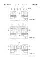
- FIG. 1depicts a partial cross-sectional view of a semiconductor topography according to an embodiment of the present invention, wherein a masking structure is formed upon a semiconductor substrate;
- FIG. 2depicts a partial cross-sectional view of the semiconductor topography, wherein a metal silicide layer is formed self-aligned to the masking structure;
- FIG. 3depicts a partial cross-sectional view of the semiconductor topography, wherein unreacted portions of the metal layer are removed from upon the masking structure;
- FIG. 4depicts a partial cross-sectional view of the semiconductor topography, wherein lightly doped drain areas are formed within the semiconductor substrate aligned with sidewalls of the masking structure;
- FIG. 5depicts a partial cross-sectional view of the semiconductor topography, wherein lightly doped drain areas are formed aligned with sidewalls of spacers formed upon the metal silicide and adjacent the sidewalls of the masking structure;
- FIG. 6depicts a partial cross-sectional view of the semiconductor topography, wherein semiconductor substrate is annealed to activate the lightly doped drain areas and the source and drain areas ;
- FIG. 7depicts a partial cross-sectional view of the semiconductor topography, wherein fill structures are formed adjacent the spacers;
- FIG. 8depicts a partial cross-sectional view of the semiconductor topography, wherein the masking structure is removed
- FIG. 9adepicts a partial cross-sectional view of the semiconductor topography, wherein a dielectric is formed upon exposed portions of the semiconductor substrate and upon the fill structures;
- FIG. 9bdepicts a partial cross-sectional view of the semiconductor topography according to an alternate embodiment, wherein a dielectric is formed upon exposed portions of the semiconductor substrate;
- FIG. 10depicts a partial cross-sectional view of the semiconductor topography, wherein a conductive gate material is deposited upon the dielectric;
- FIG. 11depicts a partial cross-sectional view of the semiconductor topography, wherein the conductive gate material is planarized to form a gate conductor;
- FIG. 12depicts a partial cross-sectional view of the semiconductor topography, wherein contacts are formed within the fill structures
- FIG. 13depicts a partial cross-sectional view of the semiconductor topography according to an alternative embodiment, wherein the fill structures are removed.
- FIG. 14depicts a partial cross-sectional view of the semiconductor topography, wherein an interlevel dielectric is formed upon the gate conductor, the spacers, and exposed portions of the silicide.
- FIG. 1depicts a semiconductor substrate 10 on which a masking layer 12 has been deposited.
- masking layer 12has a thickness between about 800 angstroms and about 2000 angstroms.
- Masking layer 12preferably includes a non-silicon-rich material.
- Masking layer 12may include a dielectric such as silicon dioxide, silicon nitride, or silicon oxynitride. The dielectric may be deposited using, e.g., chemical-vapor deposition.
- masking layer 12has been patterned and etched using, e.g., photolithography techniques that are well known in the art to selectively remove portions of the masking layer (shown in phantom). Portions of masking layer 12 that remain following the etch form masking structure 14 upon semiconductor substrate 10.
- metal layer 16may then be deposited across masking structure 14 and semiconductor substrate 10 as shown in FIG. 2.
- metal layer 16may include cobalt deposited by, e.g., sputtering or metal organic chemical-vapor deposition.
- metal layer 16may include nickel or a refractory metal, such as titanium.
- metal layer 14has a thickness between about 100 angstroms and about 300 angstroms.
- the upper surface of semiconductor substrate 10may be cleaned prior to deposition of metal layer 16 using, for example, the well-known RCA method.
- thermal radiation 18may be used to anneal semiconductor substrate 10 and the metal layer, as shown in FIG. 3, to form silicide layer 20 upon semiconductor substrate 10 and self-aligned with sidewalls of masking structures 14.
- silicide layer 20has a thickness between about 200 angstroms and about 600 angstroms. Because masking structures 14 are formed from a non-silicon-rich material, silicon is not available for reaction with the metal layer. As such, silicide is not expected to form upon the masking structure 14. Because titanium, however, is able to form a silicide when it is annealed in the presence of silicon dioxide, metal layer 16 should not include titanium when masking structure 14 includes silicon dioxide.
- Annealingpreferably occurs in a rapid thermal processing chamber at a temperature between about 600° C. and about 700° C. for about 15-60 seconds. Annealing may also occur in a tube furnace for about 5-30 minutes at a temperature of about 650°-850° C.
- the annealing ambientis preferably an inert ambient, which may contain nitrogen, helium, and/or argon. Following the anneal, unreacted metal may be removed from masking structure 14 using, e.g., a wet etch selective for the unreacted metal.
- lightly doped drain impurity areas 24may be formed by, e.g., implanting first impurity ions 22 at a first energy and a first concentration into semiconductor substrate 10 self-aligned with sidewall surfaces of masking structure 14.
- first impurity ions 22may be implanted at a concentration of between about 8.0 ⁇ 10 14 cm -2 and about 3.0 ⁇ 10 15 cm -2 and an energy of between about 0.5 keV and 5.0 keV.
- Spacers 26may then be formed adjacent sidewall surfaces of masking structure 14 by, e.g., deposition and selective etching of a conformal dielectric, as is well known in the art.
- the spacerspreferably have a lateral thickness between about 200 angstroms and about 500 angstroms.
- Spacers 26, depicted in FIG. 5,preferably include a dielectric material having etch characteristics differing from the etch characteristics of masking structure 14 such that the spacers may be retained during subsequent removal of the masking structure.
- masking structure 14includes silicon dioxide
- spacers 26preferably include a material such as silicon nitride.
- Other LDD processesmay also be employed, such as asymmetric processes, multiple LDD processes, etc. Generally, any LDD process may be employed. Also, in some embodiments, an LDD process may not be used at all. Source/drain regions may be formed aligned with the sidewalls of masking structure 14. In such an embodiment, spacers 26 may be omitted.
- Source and drain impurity areas 30may then be formed in semiconductor substrate 10 self-aligned with sidewalls of spacers 26 by, e.g., implanting second impurity ions 28 at a second energy greater than the first energy and a second concentration greater than the first concentration, as is shown in FIG. 5.
- second impurity ionsmay be implanted at a concentration between about 2.0 ⁇ 10 15 cm -2 and about 8.0 ⁇ 10 15 cm -2 and at an energy between about 1 keV and 10 keV.
- Lightly doped drain areas 24 and source and drain areas 30may then be annealed using radiation 32, as shown in FIG. 6. The second anneal may be performed in a rapid thermal processing chamber at temperatures between about 750° C. and about 950° C.
- the second annealpreferably serves to activate the dopants and to repair damage to the semiconductor substrate caused by ion implantation.
- fill material 34may be formed across the masking structure 14, the spacers 26, and the silicide layer 20, as depicted in FIG. 7.
- Fill material 34may be removed (using, e.g., chemical-mechanical polish) to a level commensurate with an upper surface of masking structure 14 to form fill structures 36 adjacent spacers 26. Removed portions of fill material 34 are shown in phantom in FIG. 7.
- fill structures 36may include a metal such as titanium or aluminum. Titanium is a preferred fill material because it is good conductor and makes good contact with the underlying silicide, especially cobalt silicide. Titanium also advantageously forms a silicide that may be used to replace or augment silicide damaged during the dopant implants and anneals.
- fill structures 36may include a dielectric material having etch characteristics differing from the etch characteristics of masking structure 14 and spacers 26.
- fill structures 36may include silicon oxynitride.
- fill structures 36may include a dielectric material having a dielectric constant greater than 3.8 (the dielectric constant of silicon dioxide), and preferably greater than about 20, such as barium strontium titanate, barium zirconate titanate, lead zirconate titanate, lead lanthanum zirconate titanate, cerium oxide, tin oxide, strontium bismuth tantalate, or tantalum oxide.
- fill structures 36may include a material having a dielectric constant less than about 3.8, such as fluorosilicate glass (FSG), silicon oxyfluoride, hydrogen silsesquioxane, fluorinated polysilicon, poly phenylquinoxaline, polyqunoline, methysilsesquioxane polymer, or fluoro-polymide.
- FSGfluorosilicate glass
- silicon oxyfluoridesilicon oxyfluoride
- hydrogen silsesquioxanefluorinated polysilicon
- poly phenylquinoxalinepolyqunoline
- methysilsesquioxane polymeror fluoro-polymide.
- a material having a low dielectric constantis preferred to a material having a high dielectric constant if a dielectric material is used to form the fill structures 36, such that the fill structures may be retained as interlevel dielectrics with good insulating properties through subsequent processing steps.
- masking structure 14may be removed from between spacers 26 using, e.g., a wet etch selective for the masking material, to form an opening 38 between the spacers.
- the masking structuremay be removed using an isotropic plasma etch.
- a photoresistmay be patterned upon the semiconductor topography using as a mask the reverse of the mask used originally to pattern masking structure 14, so that only the masking structure is exposed to the etchant.
- a conformal dielectricmay be deposited upon the exposed portions of the semiconductor substrate 10 and the spacers 26 and across the fill structures 36, as shown in FIG. 9a.
- the conformal dielectricpreferably includes gate dielectric 40 upon the upper surface of semiconductor 10; spacer dielectrics 42 adjacent sidewall surfaces of spacers 26; and capping dielectrics 44 upon upper surfaces of the fill structures 36.
- the dielectrics 40, 42, and 44include silicon dioxide.
- a gate dielectric 46may be grown upon the exposed upper surface of semiconductor substrate 10, as shown in FIG. 9b, by, e.g., annealing in the presence of thermal radiation 48. The anneal may be performed in an oxidizing ambient such that gate dielectric 46 includes silicon dioxide.
- the gate dielectricis formed to a thickness of between about 14 angstroms and about 25 angstroms.
- a conductive gate materialmay be formed within opening 38 and above fill structures 36, as depicted in FIG. 10.
- conductive gate material 50may include polysilicon.
- conductive gate material 50may include a metal such as tungsten. It should be noted that although FIG. 10 and subsequent figures depict dielectrics 40, 42, and 44 as described with respect to FIG. 9a, the process flow described herein could apply equally to a structure having only the dielectric 46, as shown in FIG. 9b.
- Conductive gate material 50may then be planarized as shown in FIG. 11 using, e.g., chemical-mechanical polish, to form gate conductor 52.
- the capping dielectricpreferably serves as an etch stop during the polishing.
- the capping dielectricmay be removed during a subsequent etch step.
- the capping dielectricmay be removed during the chemicalmechanical polish.
- fill structures 36may be retained upon the silicide 20. If fill structures 36 include a conductive material such as a metal, the fill structures may serve as contacts between the source and drain regions and interconnect lines formed upon the fill structures (not shown). An additional anneal may be performed under conditions similar to the anneal described with respect to FIG. 3 at this point to replace or augment the silicide if damage has occurred as the result of the LDD and source-drain formation. If fill structures 36 include a dielectric material, the fill structures may serve as interlevel dielectrics. Contact vias may be etched in the fill structures and the vias filled with conductive material such as aluminum or cobalt to form contacts 54, as shown in FIG. 12.
- fill structures 36may be removed from upon silicide 20 and spacers 26, as shown in FIG. 13, using, e.g., a wet etch selective for the fill structure material. If the fill structures and the spacers have similar etch characteristics, spacers 26 may be removed concurrently with fill structures 36.
- a dielectric material 56may then be deposited across gate conductor 52, spacers 26, and silicide 20, as depicted in FIG. 14.
- Dielectric material 56may be planarized using, e.g., chemical-mechanical polish to form interlevel dielectric 58. Removed portions of dielectric material 56 are shown in phantom in FIG. 14. Following formation of interlevel dielectric 58, contact vias may be formed and filled with conductive material in a manner similar to that previously described to give a structure similar to the structure depicted in FIG. 12.
Landscapes
- Physics & Mathematics (AREA)
- Engineering & Computer Science (AREA)
- High Energy & Nuclear Physics (AREA)
- Condensed Matter Physics & Semiconductors (AREA)
- General Physics & Mathematics (AREA)
- Manufacturing & Machinery (AREA)
- Computer Hardware Design (AREA)
- Microelectronics & Electronic Packaging (AREA)
- Power Engineering (AREA)
- Health & Medical Sciences (AREA)
- Toxicology (AREA)
- Insulated Gate Type Field-Effect Transistor (AREA)
Abstract
Description
Claims (41)
Priority Applications (1)
| Application Number | Priority Date | Filing Date | Title |
|---|---|---|---|
| US09/173,233US6084280A (en) | 1998-10-15 | 1998-10-15 | Transistor having a metal silicide self-aligned to the gate |
Applications Claiming Priority (1)
| Application Number | Priority Date | Filing Date | Title |
|---|---|---|---|
| US09/173,233US6084280A (en) | 1998-10-15 | 1998-10-15 | Transistor having a metal silicide self-aligned to the gate |
Publications (1)
| Publication Number | Publication Date |
|---|---|
| US6084280Atrue US6084280A (en) | 2000-07-04 |
Family
ID=22631114
Family Applications (1)
| Application Number | Title | Priority Date | Filing Date |
|---|---|---|---|
| US09/173,233Expired - LifetimeUS6084280A (en) | 1998-10-15 | 1998-10-15 | Transistor having a metal silicide self-aligned to the gate |
Country Status (1)
| Country | Link |
|---|---|
| US (1) | US6084280A (en) |
Cited By (30)
| Publication number | Priority date | Publication date | Assignee | Title |
|---|---|---|---|---|
| US6222240B1 (en) | 1998-07-22 | 2001-04-24 | Advanced Micro Devices, Inc. | Salicide and gate dielectric formed from a single layer of refractory metal |
| US6410967B1 (en) | 1998-10-15 | 2002-06-25 | Advanced Micro Devices, Inc. | Transistor having enhanced metal silicide and a self-aligned gate electrode |
| US6441434B1 (en)* | 2000-03-31 | 2002-08-27 | Advanced Micro Devices, Inc. | Semiconductor-on-insulator body-source contact and method |
| US6525381B1 (en) | 2000-03-31 | 2003-02-25 | Advanced Micro Devices, Inc. | Semiconductor-on-insulator body-source contact using shallow-doped source, and method |
| US20030183881A1 (en)* | 2002-03-28 | 2003-10-02 | Lee Young-Ki | Methods of forming silicide layers on source/drain regions of MOS transistors and MOS transistors so formed |
| US6861350B1 (en)* | 2003-06-19 | 2005-03-01 | Advanced Micro Devices, Inc. | Method of manufacturing semiconductor device comprising silicon-rich tasin metal gate electrode |
| GB2409932A (en)* | 2004-01-09 | 2005-07-13 | Ibm | Method of forming gate structures for semiconductor devices |
| US20050205896A1 (en)* | 2004-03-18 | 2005-09-22 | Hong-Jyh Li | Transistor with dopant-bearing metal in source and drain |
| US20050280104A1 (en)* | 2004-06-17 | 2005-12-22 | Hong-Jyh Li | CMOS transistor with dual high-k gate dielectric and method of manufacture thereof |
| US20050282329A1 (en)* | 2004-06-17 | 2005-12-22 | Hong-Jyh Li | CMOS transistors with dual high-k gate dielectric and methods of manufacture thereof |
| US20060084248A1 (en)* | 2004-10-15 | 2006-04-20 | Pushkar Ranade | Methods of optimization of implant conditions to minimize channeling and structures formed thereby |
| US20060118879A1 (en)* | 2004-12-06 | 2006-06-08 | Hong-Jyh Li | CMOS transistor and method of manufacture thereof |
| US20060131652A1 (en)* | 2004-12-20 | 2006-06-22 | Hong-Jyh Li | Transistor device and method of manufacture thereof |
| US20060234433A1 (en)* | 2005-04-14 | 2006-10-19 | Hongfa Luan | Transistors and methods of manufacture thereof |
| US20070026592A1 (en)* | 2005-07-13 | 2007-02-01 | Magnachip Semiconductor, Ltd | Semiconductor device and method for manufacturing the same |
| US20070052037A1 (en)* | 2005-09-02 | 2007-03-08 | Hongfa Luan | Semiconductor devices and methods of manufacture thereof |
| US20070052036A1 (en)* | 2005-09-02 | 2007-03-08 | Hongfa Luan | Transistors and methods of manufacture thereof |
| US20070075351A1 (en)* | 2005-09-30 | 2007-04-05 | Thomas Schulz | Semiconductor devices and methods of manufacture thereof |
| US20070075384A1 (en)* | 2005-03-21 | 2007-04-05 | Hongfa Luan | Transistor device and methods of manufacture thereof |
| US20070111448A1 (en)* | 2005-11-15 | 2007-05-17 | Hong-Jyh Li | Semiconductor devices and methods of manufacture thereof |
| KR100722936B1 (en) | 2006-05-04 | 2007-05-30 | 삼성전자주식회사 | MOS field effect transistor and its manufacturing method |
| US20070131972A1 (en)* | 2005-12-14 | 2007-06-14 | Hong-Jyh Li | Semiconductor devices and methods of manufacture thereof |
| US20070141797A1 (en)* | 2005-12-16 | 2007-06-21 | Hong-Jyh Li | Semiconductor devices and methods of manufacture thereof |
| US20070148842A1 (en)* | 2005-12-28 | 2007-06-28 | Pyoung On Cho | Method of manufacturing a transistor |
| US20080050898A1 (en)* | 2006-08-23 | 2008-02-28 | Hongfa Luan | Semiconductor devices and methods of manufacture thereof |
| US20090214869A1 (en)* | 2008-02-14 | 2009-08-27 | Zeon Corporation | Method for producing retardation film |
| US20110097884A1 (en)* | 2008-08-07 | 2011-04-28 | Texas Instruments Incorporated | Method to attain low defectivity fully silicided gates |
| CN102487085A (en)* | 2010-12-01 | 2012-06-06 | 中国科学院微电子研究所 | Semiconductor device and method for manufacturing the same |
| US20180068857A1 (en)* | 2016-09-08 | 2018-03-08 | International Business Machines Corporation | Low resistance source-drain contacts using high temperature silicides |
| CN111883595A (en)* | 2020-08-31 | 2020-11-03 | 上海华虹宏力半导体制造有限公司 | LDMOS device and manufacturing method thereof |
Citations (17)
| Publication number | Priority date | Publication date | Assignee | Title |
|---|---|---|---|---|
| DE1923279A1 (en)* | 1969-05-07 | 1970-12-23 | Licentia Gmbh | Transistor with an isolated control electrode |
| JPS59215774A (en)* | 1983-05-23 | 1984-12-05 | Fujitsu Ltd | Semiconductor device |
| US4683645A (en)* | 1985-06-28 | 1987-08-04 | Northern Telecom Limited | Process of fabricating MOS devices having shallow source and drain junctions |
| US4731339A (en)* | 1986-08-25 | 1988-03-15 | Rockwell International Corporation | Process for manufacturing metal-semiconductor field-effect transistors |
| US4992387A (en)* | 1989-03-27 | 1991-02-12 | Matsushita Electric Industrial Co., Ltd. | Method for fabrication of self-aligned asymmetric field effect transistors |
| US5252502A (en)* | 1992-08-03 | 1993-10-12 | Texas Instruments Incorporated | Method of making MOS VLSI semiconductor device with metal gate |
| US5268590A (en)* | 1989-12-27 | 1993-12-07 | Motorola, Inc. | CMOS device and process |
| EP0614226A1 (en)* | 1992-10-05 | 1994-09-07 | Texas Instruments Incorporated | Gate electrode using stacked layers of TiN and polysilicon |
| US5445977A (en)* | 1992-04-24 | 1995-08-29 | Matsushita Electric Industrial Co., Ltd. | Method of fabricating a Schottky field effect transistor |
| US5576227A (en)* | 1994-11-02 | 1996-11-19 | United Microelectronics Corp. | Process for fabricating a recessed gate MOS device |
| US5583067A (en)* | 1993-01-22 | 1996-12-10 | Intel Corporation | Inverse T-gate semiconductor device with self-aligned punchthrough stops and method of fabrication |
| US5646435A (en)* | 1995-04-04 | 1997-07-08 | Taiwan Semiconductor Manufacturing Company, Ltd. | Method for fabricating CMOS field effect transistors having sub-quarter micrometer channel lengths with improved short channel effect characteristics |
| US5654570A (en)* | 1995-04-19 | 1997-08-05 | International Business Machines Corporation | CMOS gate stack |
| US5717254A (en)* | 1993-09-20 | 1998-02-10 | Fujitsu Limited | Semiconductor device including a plurality of transistors |
| US5821594A (en)* | 1997-02-25 | 1998-10-13 | Nec Corporation | Semiconductor device having a self-aligned type contact hole |
| US5834811A (en)* | 1996-06-17 | 1998-11-10 | Taiwan Semiconductor Manufacturing Company, Ltd. | Salicide process for FETs |
| US5918130A (en)* | 1997-09-08 | 1999-06-29 | Advanced Micro Devices, Inc. | Transistor fabrication employing formation of silicide across source and drain regions prior to formation of the gate conductor |
- 1998
- 1998-10-15USUS09/173,233patent/US6084280A/ennot_activeExpired - Lifetime
Patent Citations (17)
| Publication number | Priority date | Publication date | Assignee | Title |
|---|---|---|---|---|
| DE1923279A1 (en)* | 1969-05-07 | 1970-12-23 | Licentia Gmbh | Transistor with an isolated control electrode |
| JPS59215774A (en)* | 1983-05-23 | 1984-12-05 | Fujitsu Ltd | Semiconductor device |
| US4683645A (en)* | 1985-06-28 | 1987-08-04 | Northern Telecom Limited | Process of fabricating MOS devices having shallow source and drain junctions |
| US4731339A (en)* | 1986-08-25 | 1988-03-15 | Rockwell International Corporation | Process for manufacturing metal-semiconductor field-effect transistors |
| US4992387A (en)* | 1989-03-27 | 1991-02-12 | Matsushita Electric Industrial Co., Ltd. | Method for fabrication of self-aligned asymmetric field effect transistors |
| US5268590A (en)* | 1989-12-27 | 1993-12-07 | Motorola, Inc. | CMOS device and process |
| US5445977A (en)* | 1992-04-24 | 1995-08-29 | Matsushita Electric Industrial Co., Ltd. | Method of fabricating a Schottky field effect transistor |
| US5252502A (en)* | 1992-08-03 | 1993-10-12 | Texas Instruments Incorporated | Method of making MOS VLSI semiconductor device with metal gate |
| EP0614226A1 (en)* | 1992-10-05 | 1994-09-07 | Texas Instruments Incorporated | Gate electrode using stacked layers of TiN and polysilicon |
| US5583067A (en)* | 1993-01-22 | 1996-12-10 | Intel Corporation | Inverse T-gate semiconductor device with self-aligned punchthrough stops and method of fabrication |
| US5717254A (en)* | 1993-09-20 | 1998-02-10 | Fujitsu Limited | Semiconductor device including a plurality of transistors |
| US5576227A (en)* | 1994-11-02 | 1996-11-19 | United Microelectronics Corp. | Process for fabricating a recessed gate MOS device |
| US5646435A (en)* | 1995-04-04 | 1997-07-08 | Taiwan Semiconductor Manufacturing Company, Ltd. | Method for fabricating CMOS field effect transistors having sub-quarter micrometer channel lengths with improved short channel effect characteristics |
| US5654570A (en)* | 1995-04-19 | 1997-08-05 | International Business Machines Corporation | CMOS gate stack |
| US5834811A (en)* | 1996-06-17 | 1998-11-10 | Taiwan Semiconductor Manufacturing Company, Ltd. | Salicide process for FETs |
| US5821594A (en)* | 1997-02-25 | 1998-10-13 | Nec Corporation | Semiconductor device having a self-aligned type contact hole |
| US5918130A (en)* | 1997-09-08 | 1999-06-29 | Advanced Micro Devices, Inc. | Transistor fabrication employing formation of silicide across source and drain regions prior to formation of the gate conductor |
Non-Patent Citations (4)
| Title |
|---|
| Wolf et al., "Silicon Processing For the VLSI Era, vol. 1: Process Technology," Lattice Press, Sunset Beach, California, 1986, pp. 384-406, and pp. 516-518, 1986. |
| Wolf et al., "Silicon Processing For the VLSI Era, vol. 2: Process Techology," Lattice Press, Sunset Beach, California, 1990, pp. 143-152, 1990. |
| Wolf et al., Silicon Processing For the VLSI Era, vol. 1: Process Technology, Lattice Press, Sunset Beach, California, 1986, pp. 384 406, and pp. 516 518, 1986.* |
| Wolf et al., Silicon Processing For the VLSI Era, vol. 2: Process Techology, Lattice Press, Sunset Beach, California, 1990, pp. 143 152, 1990.* |
Cited By (82)
| Publication number | Priority date | Publication date | Assignee | Title |
|---|---|---|---|---|
| US6222240B1 (en) | 1998-07-22 | 2001-04-24 | Advanced Micro Devices, Inc. | Salicide and gate dielectric formed from a single layer of refractory metal |
| US6410967B1 (en) | 1998-10-15 | 2002-06-25 | Advanced Micro Devices, Inc. | Transistor having enhanced metal silicide and a self-aligned gate electrode |
| US6441434B1 (en)* | 2000-03-31 | 2002-08-27 | Advanced Micro Devices, Inc. | Semiconductor-on-insulator body-source contact and method |
| US6525381B1 (en) | 2000-03-31 | 2003-02-25 | Advanced Micro Devices, Inc. | Semiconductor-on-insulator body-source contact using shallow-doped source, and method |
| US6790750B1 (en) | 2000-03-31 | 2004-09-14 | Advanced Micro Devices, Inc. | Semiconductor-on-insulator body-source contact and method |
| US20030183881A1 (en)* | 2002-03-28 | 2003-10-02 | Lee Young-Ki | Methods of forming silicide layers on source/drain regions of MOS transistors and MOS transistors so formed |
| US7211515B2 (en)* | 2002-03-28 | 2007-05-01 | Samsung Electronics Co., Ltd. | Methods of forming silicide layers on source/drain regions of MOS transistors |
| US20070170501A1 (en)* | 2002-03-28 | 2007-07-26 | Lee Young-Ki | MOS Transistors Including Silicide Layers on Source/Drain Regions |
| US6861350B1 (en)* | 2003-06-19 | 2005-03-01 | Advanced Micro Devices, Inc. | Method of manufacturing semiconductor device comprising silicon-rich tasin metal gate electrode |
| GB2409932A (en)* | 2004-01-09 | 2005-07-13 | Ibm | Method of forming gate structures for semiconductor devices |
| GB2409932B (en)* | 2004-01-09 | 2006-10-25 | Ibm | Method of forming gate structures for semiconductor devices |
| CN1670965B (en)* | 2004-03-18 | 2011-01-12 | 因芬尼昂技术股份公司 | Transistors with doped metals in the source and drain |
| US20090026555A1 (en)* | 2004-03-18 | 2009-01-29 | Hong-Jyh Li | Transistor with Dopant-Bearing Metal in Source and Drain |
| US7446379B2 (en)* | 2004-03-18 | 2008-11-04 | Infineon Technologies Ag | Transistor with dopant-bearing metal in source and drain |
| US8390080B2 (en)* | 2004-03-18 | 2013-03-05 | Infineon Technologies Ag | Transistor with dopant-bearing metal in source and drain |
| US20050205896A1 (en)* | 2004-03-18 | 2005-09-22 | Hong-Jyh Li | Transistor with dopant-bearing metal in source and drain |
| US8637357B2 (en) | 2004-06-17 | 2014-01-28 | Infineon Technologies Ag | CMOS Transistor with dual high-k gate dielectric and method of manufacture thereof |
| US8178902B2 (en) | 2004-06-17 | 2012-05-15 | Infineon Technologies Ag | CMOS transistor with dual high-k gate dielectric and method of manufacture thereof |
| US7592678B2 (en) | 2004-06-17 | 2009-09-22 | Infineon Technologies Ag | CMOS transistors with dual high-k gate dielectric and methods of manufacture thereof |
| US20050282329A1 (en)* | 2004-06-17 | 2005-12-22 | Hong-Jyh Li | CMOS transistors with dual high-k gate dielectric and methods of manufacture thereof |
| US20050280104A1 (en)* | 2004-06-17 | 2005-12-22 | Hong-Jyh Li | CMOS transistor with dual high-k gate dielectric and method of manufacture thereof |
| US9269635B2 (en) | 2004-06-17 | 2016-02-23 | Infineon Technologies Ag | CMOS Transistor with dual high-k gate dielectric |
| US8476678B2 (en) | 2004-06-17 | 2013-07-02 | Infineon Technologies Ag | CMOS Transistor with dual high-k gate dielectric |
| US8729633B2 (en) | 2004-06-17 | 2014-05-20 | Infineon Technologies Ag | CMOS transistor with dual high-k gate dielectric |
| US20060084248A1 (en)* | 2004-10-15 | 2006-04-20 | Pushkar Ranade | Methods of optimization of implant conditions to minimize channeling and structures formed thereby |
| US20060202267A1 (en)* | 2004-10-15 | 2006-09-14 | Pushkar Ranade | Methods of optimization of implant conditions to minimize channeling and structures formed thereby |
| US20060118879A1 (en)* | 2004-12-06 | 2006-06-08 | Hong-Jyh Li | CMOS transistor and method of manufacture thereof |
| US20080116523A1 (en)* | 2004-12-06 | 2008-05-22 | Hong-Jyh Li | CMOS transistor and method of manufacture thereof |
| US7709901B2 (en) | 2004-12-06 | 2010-05-04 | Infineon Technologies Ag | CMOS transistor and method of manufacture thereof |
| US7344934B2 (en) | 2004-12-06 | 2008-03-18 | Infineon Technologies Ag | CMOS transistor and method of manufacture thereof |
| US8399934B2 (en) | 2004-12-20 | 2013-03-19 | Infineon Technologies Ag | Transistor device |
| US8669154B2 (en) | 2004-12-20 | 2014-03-11 | Infineon Technologies Ag | Transistor device and method of manufacture thereof |
| US20080233694A1 (en)* | 2004-12-20 | 2008-09-25 | Hong-Jyh Li | Transistor Device and Method of Manufacture Thereof |
| US7964460B2 (en) | 2004-12-20 | 2011-06-21 | Infineon Technologies Ag | Method of manufacturing an NMOS device and a PMOS device |
| US8685814B2 (en) | 2004-12-20 | 2014-04-01 | Infineon Technologies Ag | Transistor device and method of manufacture thereof |
| US20060131652A1 (en)* | 2004-12-20 | 2006-06-22 | Hong-Jyh Li | Transistor device and method of manufacture thereof |
| US20110223728A1 (en)* | 2004-12-20 | 2011-09-15 | Hong-Jyh Li | Transistor Device and Method of Manufacture Thereof |
| US8017484B2 (en) | 2005-03-21 | 2011-09-13 | Infineon Technologies Ag | Transistor device and methods of manufacture thereof |
| US20070075384A1 (en)* | 2005-03-21 | 2007-04-05 | Hongfa Luan | Transistor device and methods of manufacture thereof |
| US8269289B2 (en) | 2005-03-21 | 2012-09-18 | Infineon Technologies Ag | Transistor device and methods of manufacture thereof |
| US7361538B2 (en) | 2005-04-14 | 2008-04-22 | Infineon Technologies Ag | Transistors and methods of manufacture thereof |
| US20080164536A1 (en)* | 2005-04-14 | 2008-07-10 | Hongfa Luan | Transistors and Methods of Manufacture Thereof |
| US20060234433A1 (en)* | 2005-04-14 | 2006-10-19 | Hongfa Luan | Transistors and methods of manufacture thereof |
| US7413956B2 (en) | 2005-07-13 | 2008-08-19 | Magnachip Semiconductor, Ltd. | Semiconductor device manufacturing method |
| US20070026592A1 (en)* | 2005-07-13 | 2007-02-01 | Magnachip Semiconductor, Ltd | Semiconductor device and method for manufacturing the same |
| US20070052037A1 (en)* | 2005-09-02 | 2007-03-08 | Hongfa Luan | Semiconductor devices and methods of manufacture thereof |
| US20070052036A1 (en)* | 2005-09-02 | 2007-03-08 | Hongfa Luan | Transistors and methods of manufacture thereof |
| US8188551B2 (en) | 2005-09-30 | 2012-05-29 | Infineon Technologies Ag | Semiconductor devices and methods of manufacture thereof |
| US9659962B2 (en) | 2005-09-30 | 2017-05-23 | Infineon Technologies Ag | Semiconductor devices and methods of manufacture thereof |
| US8722473B2 (en) | 2005-09-30 | 2014-05-13 | Infineon Technologies Ag | Semiconductor devices and methods of manufacture thereof |
| US20070075351A1 (en)* | 2005-09-30 | 2007-04-05 | Thomas Schulz | Semiconductor devices and methods of manufacture thereof |
| US20070111448A1 (en)* | 2005-11-15 | 2007-05-17 | Hong-Jyh Li | Semiconductor devices and methods of manufacture thereof |
| US7755144B2 (en) | 2005-11-15 | 2010-07-13 | Infineon Technologies Ag | Multiple-gate MOS transistors |
| US7462538B2 (en) | 2005-11-15 | 2008-12-09 | Infineon Technologies Ag | Methods of manufacturing multiple gate CMOS transistors having different gate dielectric materials |
| US20100129968A1 (en)* | 2005-11-15 | 2010-05-27 | Hong-Jyh Li | Semiconductor Devices and Methods of Manufacture Thereof |
| US20090065870A1 (en)* | 2005-11-15 | 2009-03-12 | Hong-Jyh Li | Semiconductor Devices and Methods of Manufacture Thereof |
| US7749832B2 (en) | 2005-12-14 | 2010-07-06 | Infineon Technologies Ag | Semiconductor devices and methods of manufacture thereof |
| US7973369B2 (en) | 2005-12-14 | 2011-07-05 | Infineon Technologies Ag | Semiconductor devices and methods of manufacture thereof |
| US20090146217A1 (en)* | 2005-12-14 | 2009-06-11 | Hong-Jyh Li | Semiconductor Devices and Methods of Manufacture Thereof |
| US20070131972A1 (en)* | 2005-12-14 | 2007-06-14 | Hong-Jyh Li | Semiconductor devices and methods of manufacture thereof |
| US8169033B2 (en) | 2005-12-14 | 2012-05-01 | Infineon Technologies Ag | Semiconductor devices and methods of manufacture thereof |
| US7495290B2 (en) | 2005-12-14 | 2009-02-24 | Infineon Technologies Ag | Semiconductor devices and methods of manufacture thereof |
| US8004047B2 (en) | 2005-12-16 | 2011-08-23 | Infineon Technologies Ag | Semiconductor devices and methods of manufacture thereof |
| US20090166752A1 (en)* | 2005-12-16 | 2009-07-02 | Hong-Jyh Li | Semiconductor Devices and Methods of Manufacture Thereof |
| US20070141797A1 (en)* | 2005-12-16 | 2007-06-21 | Hong-Jyh Li | Semiconductor devices and methods of manufacture thereof |
| US7510943B2 (en) | 2005-12-16 | 2009-03-31 | Infineon Technologies Ag | Semiconductor devices and methods of manufacture thereof |
| US7700451B2 (en)* | 2005-12-28 | 2010-04-20 | Dongbu Hitek Co., Ltd. | Method of manufacturing a transistor |
| US20070148842A1 (en)* | 2005-12-28 | 2007-06-28 | Pyoung On Cho | Method of manufacturing a transistor |
| US20070257303A1 (en)* | 2006-05-04 | 2007-11-08 | Samsung Electronics., Ltd. | Transistor and method for forming the same |
| KR100722936B1 (en) | 2006-05-04 | 2007-05-30 | 삼성전자주식회사 | MOS field effect transistor and its manufacturing method |
| US20080050898A1 (en)* | 2006-08-23 | 2008-02-28 | Hongfa Luan | Semiconductor devices and methods of manufacture thereof |
| US20090214869A1 (en)* | 2008-02-14 | 2009-08-27 | Zeon Corporation | Method for producing retardation film |
| US8273645B2 (en)* | 2008-08-07 | 2012-09-25 | Texas Instruments Incorporated | Method to attain low defectivity fully silicided gates |
| US20110097884A1 (en)* | 2008-08-07 | 2011-04-28 | Texas Instruments Incorporated | Method to attain low defectivity fully silicided gates |
| CN102487085B (en)* | 2010-12-01 | 2014-04-23 | 中国科学院微电子研究所 | Semiconductor device and method for manufacturing the same |
| CN102487085A (en)* | 2010-12-01 | 2012-06-06 | 中国科学院微电子研究所 | Semiconductor device and method for manufacturing the same |
| US20180068857A1 (en)* | 2016-09-08 | 2018-03-08 | International Business Machines Corporation | Low resistance source-drain contacts using high temperature silicides |
| US10685888B2 (en) | 2016-09-08 | 2020-06-16 | International Business Machines Corporation | Low resistance source-drain contacts using high temperature silicides |
| US10825740B2 (en) | 2016-09-08 | 2020-11-03 | International Business Machines Corporation | Low resistance source-drain contacts using high temperature silicides |
| US11062956B2 (en) | 2016-09-08 | 2021-07-13 | International Business Machines Corporation | Low resistance source-drain contacts using high temperature silicides |
| US11088033B2 (en)* | 2016-09-08 | 2021-08-10 | International Business Machines Corporation | Low resistance source-drain contacts using high temperature silicides |
| CN111883595A (en)* | 2020-08-31 | 2020-11-03 | 上海华虹宏力半导体制造有限公司 | LDMOS device and manufacturing method thereof |
Similar Documents
| Publication | Publication Date | Title |
|---|---|---|
| US6084280A (en) | Transistor having a metal silicide self-aligned to the gate | |
| US6710413B2 (en) | Salicide field effect transistors with improved borderless contact structures and a method of fabrication | |
| US6200865B1 (en) | Use of sacrificial dielectric structure to form semiconductor device with a self-aligned threshold adjust and overlying low-resistance gate | |
| US5352631A (en) | Method for forming a transistor having silicided regions | |
| US6258680B1 (en) | Integrated circuit gate conductor which uses layered spacers to produce a graded junction | |
| US6329256B1 (en) | Self-aligned damascene gate formation with low gate resistance | |
| US5731239A (en) | Method of making self-aligned silicide narrow gate electrodes for field effect transistors having low sheet resistance | |
| US5710450A (en) | Transistor with ultra shallow tip and method of fabrication | |
| US6403434B1 (en) | Process for manufacturing MOS transistors having elevated source and drain regions and a high-k gate dielectric | |
| US6495437B1 (en) | Low temperature process to locally form high-k gate dielectrics | |
| US6806534B2 (en) | Damascene method for improved MOS transistor | |
| US6911384B2 (en) | Gate structure with independently tailored vertical doping profile | |
| US6180501B1 (en) | Method to fabricate a double-polysilicon gate structure for a sub-quarter micron self-aligned-titanium silicide process | |
| US5798278A (en) | Method of forming raised source/drain regions in an integrated circuit | |
| US6372589B1 (en) | Method of forming ultra-shallow source/drain extension by impurity diffusion from doped dielectric spacer | |
| US5949126A (en) | Trench isolation structure employing protective sidewall spacers upon exposed surfaces of the isolation trench | |
| US5994193A (en) | Method of making high performance MOSFET with integrated poly/metal gate electrode | |
| US6524920B1 (en) | Low temperature process for a transistor with elevated source and drain | |
| KR101400326B1 (en) | Silicided polysilicon spacer for enhanced contact area | |
| US6756277B1 (en) | Replacement gate process for transistors having elevated source and drain regions | |
| US7009258B2 (en) | Method of building a CMOS structure on thin SOI with source/drain electrodes formed by in situ doped selective amorphous silicon | |
| US6326251B1 (en) | Method of making salicidation of source and drain regions with metal gate MOSFET | |
| US5981365A (en) | Stacked poly-oxide-poly gate for improved silicide formation | |
| EP1138058B1 (en) | Method of manufacturing a semiconductor device having a gate with a varying work function | |
| US20020090787A1 (en) | Self-aligned elevated transistor |
Legal Events
| Date | Code | Title | Description |
|---|---|---|---|
| AS | Assignment | Owner name:ADVANCED MICRO DEVICES, INC., CALIFORNIA Free format text:ASSIGNMENT OF ASSIGNORS INTEREST;ASSIGNORS:HAUSE, FREDERICK N.;GARDNER, MARK I.;MAY, CHARLES E.;REEL/FRAME:009526/0875 Effective date:19981007 | |
| STCF | Information on status: patent grant | Free format text:PATENTED CASE | |
| FPAY | Fee payment | Year of fee payment:4 | |
| FPAY | Fee payment | Year of fee payment:8 | |
| AS | Assignment | Owner name:GLOBALFOUNDRIES INC., CAYMAN ISLANDS Free format text:AFFIRMATION OF PATENT ASSIGNMENT;ASSIGNOR:ADVANCED MICRO DEVICES, INC.;REEL/FRAME:023119/0083 Effective date:20090630 Owner name:GLOBALFOUNDRIES INC., CAYMAN ISLANDS Free format text:AFFIRMATION OF PATENT ASSIGNMENT;ASSIGNOR:ADVANCED MICRO DEVICES, INC.;REEL/FRAME:023120/0426 Effective date:20090630 Owner name:GLOBALFOUNDRIES INC.,CAYMAN ISLANDS Free format text:AFFIRMATION OF PATENT ASSIGNMENT;ASSIGNOR:ADVANCED MICRO DEVICES, INC.;REEL/FRAME:023120/0426 Effective date:20090630 | |
| FPAY | Fee payment | Year of fee payment:12 | |
| AS | Assignment | Owner name:WILMINGTON TRUST, NATIONAL ASSOCIATION, DELAWARE Free format text:SECURITY AGREEMENT;ASSIGNOR:GLOBALFOUNDRIES INC.;REEL/FRAME:049490/0001 Effective date:20181127 | |
| AS | Assignment | Owner name:GLOBALFOUNDRIES INC., CAYMAN ISLANDS Free format text:RELEASE BY SECURED PARTY;ASSIGNOR:WILMINGTON TRUST, NATIONAL ASSOCIATION;REEL/FRAME:054636/0001 Effective date:20201117 | |
| AS | Assignment | Owner name:GLOBALFOUNDRIES U.S. INC., NEW YORK Free format text:RELEASE BY SECURED PARTY;ASSIGNOR:WILMINGTON TRUST, NATIONAL ASSOCIATION;REEL/FRAME:056987/0001 Effective date:20201117 |