US6083844A - Techniques for etching an oxide layer - Google Patents
Techniques for etching an oxide layerDownload PDFInfo
- Publication number
- US6083844A US6083844AUS08/996,071US99607197AUS6083844AUS 6083844 AUS6083844 AUS 6083844AUS 99607197 AUS99607197 AUS 99607197AUS 6083844 AUS6083844 AUS 6083844A
- Authority
- US
- United States
- Prior art keywords
- tin
- layer
- chf
- etching
- plasma processing
- Prior art date
- Legal status (The legal status is an assumption and is not a legal conclusion. Google has not performed a legal analysis and makes no representation as to the accuracy of the status listed.)
- Expired - Lifetime
Links
- 238000000034methodMethods0.000titleclaimsabstractdescription58
- 238000005530etchingMethods0.000titleclaimsabstractdescription48
- VYPSYNLAJGMNEJ-UHFFFAOYSA-NSilicium dioxideChemical compoundO=[Si]=OVYPSYNLAJGMNEJ-UHFFFAOYSA-N0.000claimsabstractdescription80
- 238000012545processingMethods0.000claimsabstractdescription43
- 239000000758substrateSubstances0.000claimsabstractdescription41
- 229960001866silicon dioxideDrugs0.000claimsabstractdescription40
- 235000012239silicon dioxideNutrition0.000claimsabstractdescription40
- 239000000377silicon dioxideSubstances0.000claimsabstractdescription40
- XPDWGBQVDMORPB-UHFFFAOYSA-NFluoroformChemical compoundFC(F)FXPDWGBQVDMORPB-UHFFFAOYSA-N0.000claimsabstractdescription29
- 229910052754neonInorganic materials0.000claimsabstractdescription27
- GKAOGPIIYCISHV-UHFFFAOYSA-Nneon atomChemical compound[Ne]GKAOGPIIYCISHV-UHFFFAOYSA-N0.000claimsabstractdescription27
- ATJFFYVFTNAWJD-UHFFFAOYSA-NTinChemical compound[Sn]ATJFFYVFTNAWJD-UHFFFAOYSA-N0.000claimsabstract18
- 239000000463materialSubstances0.000claimsdescription21
- 239000004065semiconductorSubstances0.000claimsdescription15
- 229920000642polymerPolymers0.000claimsdescription13
- GWEVSGVZZGPLCZ-UHFFFAOYSA-NTitan oxideChemical compoundO=[Ti]=OGWEVSGVZZGPLCZ-UHFFFAOYSA-N0.000claimsdescription8
- 238000006243chemical reactionMethods0.000claimsdescription8
- OGIDPMRJRNCKJF-UHFFFAOYSA-Ntitanium oxideInorganic materials[Ti]=OOGIDPMRJRNCKJF-UHFFFAOYSA-N0.000claimsdescription8
- 229920002120photoresistant polymerPolymers0.000claimsdescription7
- BOTDANWDWHJENH-UHFFFAOYSA-NTetraethyl orthosilicateChemical groupCCO[Si](OCC)(OCC)OCCBOTDANWDWHJENH-UHFFFAOYSA-N0.000claimsdescription5
- 230000015572biosynthetic processEffects0.000claimsdescription5
- RTAQQCXQSZGOHL-UHFFFAOYSA-NTitaniumChemical compound[Ti]RTAQQCXQSZGOHL-UHFFFAOYSA-N0.000claimsdescription4
- NBVXSUQYWXRMNV-UHFFFAOYSA-NfluoromethaneChemical compoundFCNBVXSUQYWXRMNV-UHFFFAOYSA-N0.000claimsdescription4
- 239000010936titaniumSubstances0.000claimsdescription4
- 229910052719titaniumInorganic materials0.000claimsdescription4
- 239000011521glassSubstances0.000claimsdescription3
- NRTOMJZYCJJWKI-UHFFFAOYSA-NTitanium nitrideChemical compound[Ti]#NNRTOMJZYCJJWKI-UHFFFAOYSA-N0.000description50
- 239000007789gasSubstances0.000description9
- 238000001020plasma etchingMethods0.000description9
- 238000004519manufacturing processMethods0.000description4
- 230000004075alterationEffects0.000description3
- 229910052782aluminiumInorganic materials0.000description2
- XAGFODPZIPBFFR-UHFFFAOYSA-NaluminiumChemical compound[Al]XAGFODPZIPBFFR-UHFFFAOYSA-N0.000description2
- 239000006117anti-reflective coatingSubstances0.000description2
- 230000004888barrier functionEffects0.000description2
- 239000005380borophosphosilicate glassSubstances0.000description2
- 150000002500ionsChemical class0.000description2
- 239000000203mixtureSubstances0.000description2
- 230000008569processEffects0.000description2
- 238000011160researchMethods0.000description2
- 239000005368silicate glassSubstances0.000description2
- BSYNRYMUTXBXSQ-UHFFFAOYSA-NAspirinChemical compoundCC(=O)OC1=CC=CC=C1C(O)=OBSYNRYMUTXBXSQ-UHFFFAOYSA-N0.000description1
- CURLTUGMZLYLDI-UHFFFAOYSA-NCarbon dioxideChemical compoundO=C=OCURLTUGMZLYLDI-UHFFFAOYSA-N0.000description1
- RYGMFSIKBFXOCR-UHFFFAOYSA-NCopperChemical compound[Cu]RYGMFSIKBFXOCR-UHFFFAOYSA-N0.000description1
- 229910004014SiF4Inorganic materials0.000description1
- 230000000903blocking effectEffects0.000description1
- 239000006227byproductSubstances0.000description1
- IYRWEQXVUNLMAY-UHFFFAOYSA-Ncarbonyl fluorideChemical compoundFC(F)=OIYRWEQXVUNLMAY-UHFFFAOYSA-N0.000description1
- 229910052802copperInorganic materials0.000description1
- 239000010949copperSubstances0.000description1
- 230000008021depositionEffects0.000description1
- 238000001312dry etchingMethods0.000description1
- 230000003628erosive effectEffects0.000description1
- 238000002474experimental methodMethods0.000description1
- 239000003292glueSubstances0.000description1
- 230000006872improvementEffects0.000description1
- 230000001788irregularEffects0.000description1
- 230000007246mechanismEffects0.000description1
- 229910052751metalInorganic materials0.000description1
- 239000002184metalSubstances0.000description1
- 238000012544monitoring processMethods0.000description1
- 230000003287optical effectEffects0.000description1
- 238000005389semiconductor device fabricationMethods0.000description1
- ABTOQLMXBSRXSM-UHFFFAOYSA-Nsilicon tetrafluorideChemical compoundF[Si](F)(F)FABTOQLMXBSRXSM-UHFFFAOYSA-N0.000description1
- WFKWXMTUELFFGS-UHFFFAOYSA-NtungstenChemical compound[W]WFKWXMTUELFFGS-UHFFFAOYSA-N0.000description1
- 229910052721tungstenInorganic materials0.000description1
- 239000010937tungstenSubstances0.000description1
Images


Classifications
- H—ELECTRICITY
- H01—ELECTRIC ELEMENTS
- H01L—SEMICONDUCTOR DEVICES NOT COVERED BY CLASS H10
- H01L21/00—Processes or apparatus adapted for the manufacture or treatment of semiconductor or solid state devices or of parts thereof
- H01L21/02—Manufacture or treatment of semiconductor devices or of parts thereof
- H01L21/04—Manufacture or treatment of semiconductor devices or of parts thereof the devices having potential barriers, e.g. a PN junction, depletion layer or carrier concentration layer
- H01L21/18—Manufacture or treatment of semiconductor devices or of parts thereof the devices having potential barriers, e.g. a PN junction, depletion layer or carrier concentration layer the devices having semiconductor bodies comprising elements of Group IV of the Periodic Table or AIIIBV compounds with or without impurities, e.g. doping materials
- H01L21/30—Treatment of semiconductor bodies using processes or apparatus not provided for in groups H01L21/20 - H01L21/26
- H01L21/31—Treatment of semiconductor bodies using processes or apparatus not provided for in groups H01L21/20 - H01L21/26 to form insulating layers thereon, e.g. for masking or by using photolithographic techniques; After treatment of these layers; Selection of materials for these layers
- H01L21/3105—After-treatment
- H01L21/311—Etching the insulating layers by chemical or physical means
- H01L21/31105—Etching inorganic layers
- H01L21/31111—Etching inorganic layers by chemical means
- H01L21/31116—Etching inorganic layers by chemical means by dry-etching
Definitions
- the present inventionrelates to the fabrication of semiconductor integrated circuits (IC's) and flat panel displays. More particularly, the present invention relates to improved methods and apparatus for etching through the silicon dioxide-containing layer of a substrate during semiconductor device fabrication.
- TiNtitanium nitride
- ARCantireflective coating
- the TiN layerwhen the TiN layer is employed under a silicon dioxide-containing layer, such as a PETEOS (plasma enhanced tetraethylorthosilicate), BSG (boron-doped silicate glass), USG (undoped silicate glass), BPSG (borophosphosilicate glass), or the like, the TiN material may serve as an etch stop during a via etch through the silicon dioxide-containing layer. Thereafter, the TiN material may serve as a barrier or glue material between the subsequently deposited tungsten or aluminum plugs and any underlying metal layer (e.g., copper or aluminum).
- a PETEOSplasma enhanced tetraethylorthosilicate
- BSGboron-doped silicate glass
- USGundoped silicate glass
- BPSGborophosphosilicate glass
- FIG. 1illustrates a cross section view of some exemplary layers of a substrate.
- an underlying layer 102representing any layer or layers that may underlie a TiN layer on a substrate.
- underlying layer 102may represent the substrate itself or may represent layers subsequently deposited and etched prior to the deposition of a TiN layer 104.
- TiN layer 104is shown disposed between underlying layer 102 and a subsequently deposited silicon dioxide-containing layer 106.
- FIG. 1have not been shown to scale to facilitate ease of illustration, TiN layer 104 is typically much thinner than silicon dioxide-containing layer 106.
- TiN layer 104may function as the etch stop layer, i.e., it is desirable that the etching stops before TiN layer 104 is etched through.
- semiconductor devices densityincreases over time, however, it becomes increasingly difficult to etch, using prior art etch techniques, through silicon dioxide-containing layer 106 without damaging underlying TiN layer 104. This is because the TiN layer is typically quite thin in modern high density semiconductor devices since a thinner TiN layer is more conducive to the manufacture of high density devices.
- the etching of the oxide layerwas typically accomplished using a C X F Y chemistry (e.g., CF 4 , C 2 F 6 , C 3 F 8 , or the like ).
- the C X F Y chemistrywas selected primarily for its high etch rate through the oxide layer.
- the prior art C X F Y chemistrytypically etches through the oxide layer at a rate of greater than about 2,000 angstrom per minute.
- the C X F Y chemistryhas a relatively low selectivity toward TiN. That is, the prior art C X F Y chemistry also etches the TiN material at a relatively significant etch rate.
- the C X F Y chemistrytypically has an oxide-to-TiN selectivity in the range of 7 to 1 to 10 to 1 (i.e., the C X F Y etches through the oxide material 7 to 10 times as fast as it etches through the TiN material).
- a trench 108is etched through silicon dioxide-containing layer 106.
- TiN layer 104is intended as the etch stop layer and should have stopped the oxide etch before the oxide etch proceeds through to underlying layer 102. Nevertheless, the low TiN selectivity of the prior art chemistry causes TiN layer 104 of FIG. 2, which is quite thin to enable the semiconductor devices to pack closely together, to be completely etched through under trench 108. When the TiN layer is inadvertently etched through, the bottom of trench 108 may present an irregular topology to subsequent processes, which may cause the fabricated devices to fail due to, for example, unintended misalignment of layers.
- TiN layer 104may be etched through either during the main oxide etch step or during the oxide over-etch step.
- FIG. 3depicts a multi-level oxide structure 300, including a multi level oxide layer 302.
- multi-level oxide layer 302includes a thick region 304 and a thin region 306 although other regions of various thicknesses may also be present within multi-level oxide layer 302.
- Multi-level oxide layer 302is disposed on TiN layer 104, which is intended to function as an etch stop during the etching of multi-level oxide layer 302.
- underlying layer 102is also shown disposed below TiN layer 104.
- the oxide etch stepis shortened to prevent damage to the TiN material underneath the via in thin region 306, the via through thick region 304 of multi-level oxide layer 302 may not be completely etched through.
- the low oxide-to-TiN selectivity of the prior art chemistryposes serious problems while etching multi-level oxide layers of modern high density ICs.
- the improved techniquespreferably provide a high oxide-to-TiN selectivity to substantially reduce damage to the underlying TiN layer during oxide etching.
- the inventionrelates, in one embodiment, to a method for etching a substrate in a plasma processing chamber.
- the substratehas thereon a silicon dioxide-containing layer disposed above a TiN layer.
- the methodincludes positioning the substrate in the plasma processing chamber.
- an etchant source gasthat includes CO, CHF 3 , neon and N 2 into the plasma processing chamber.
- forming a plasma out of the etchant source gaswithin the plasma processing chamber to cause etching of the silicon-dioxide-containing layer.
- the inventionin another embodiment, relates to a method for preventing damage to an underlying TiN layer while etching a multi-level silicon dioxide-containing layer in a plasma processing chamber.
- the multi-level silicon dioxide-containing layeris disposed above the TiN layer on a substrate.
- the multi-level silicon dioxide-containing layerincludes a thin region and a thick region.
- the methodincludes forming a photoresist mask above the multi-level silicon-dioxide containing layer.
- the photoresist maskhas therein a first via opening above the thin region and a second via opening above the thick region.
- the methodfurther includes disposing the substrate, including the photoresist mask, in the plasma processing chamber. There is also included flowing an etchant source gas that includes CO, CHF 3 , neon and N 2 into the plasma processing chamber. Additionally, there is included providing power to electrodes of the plasma processing chamber to form a plasma out of the etchant source gas, thereby causing etching of the multi-level silicon dioxide-containing layer through the first via opening and the second via opening. During etching, the flow rates of the CO, the CHF 3 , the neon and the N 2 are configured to permit the multi-level silicon dioxide-containing layer to be completely etched through in the thick region without damaging the TiN layer under the thin region of the multilevel silicon dioxide-containing layer.
- the inventionin yet another embodiment, relates to a method for forming an integrated circuit.
- the methodincludes providing a semiconductor wafer having thereon a silicon dioxide-containing layer disposed above a TiN layer. There is also included positioning the semiconductor wafer in a plasma processing chamber. Additionally, there is included flowing an etchant source gas that includes CO, CHF 3 , neon and N 2 into the plasma processing chamber. Further, there is included forming a plasma out of the etchant source gas within the plasma processing chamber to cause etching of the silicon-dioxide-containing layer.
- FIG. 1illustrates a cross section view of some exemplary layers of a substrate, including the silicon dioxide-containing layer and the underlying TiN layer.
- FIG. 2a trench is etched through silicon dioxide-containing layer of FIG. 1.
- FIG. 3depicts an exemplary multi-level oxide structure, including a multi level oxide layer.
- FIG. 4illustrates a triode-type plasma processing system, representing a plasma processing system suitable for use with the inventive CO/CHF 3 /neon/N 2 oxide etch technique.
- FIG. 5illustrates, in accordance with one embodiment of the present invention, the steps involved in etching a substrate having thereon an oxide layer disposed above a TiN layer.
- the aforementioned TiN damage issueis substantially alleviated by etching the oxide layer (i.e., the silicon dioxide-containing layer) with a novel chemistry that includes CO, CHF 3 , neon and N 2 in a plasma processing system.
- the inventive chemistryis employed to etch through the oxide layer in a triode-type plasma processing system such as the Lam 9500TM plasma processing system available from Lam Research Corp. of Fremont, Calif.
- inventive oxide etch techniqueusing the inventive CO/CHF 3 /neon/N 2 chemistry, may be performed in any of the known plasma processing apparatuses including, but not limited to, those adapted for dry etching, plasma etching, reactive ion etching, magnetically enhanced reactive ion etching, electron cyclotron resonance etching, or the like. Note that the this is true irrespective of whether energy to the plasma is delivered through capacitively coupled parallel electrode plates, through ECR microwave plasma sources, or through inductively coupled RF sources such as helicon, helical resonators, and transformer coupled sources (either planar or non-planar). These processing systems, among others, are readily available commercially from a number of vendors including the aforementioned Lam Research Corp.
- triode-type plasma processing system 402representing a plasma processing system suitable for use with the inventive CO/CHF 3 /neon/N 2 oxide etch technique.
- triode-type plasma processing system 402includes a chamber 404. Within chamber 404, there is disposed an upper electrode 406 and a lower electrode 408.
- upper electrode 406represents a combination electrode/gas distribution plate mechanism through which etchant source gases entering through port 410 is distributed into chamber 404 through apertures 412.
- a substrate 414representing, for example, a glass panel or a semiconductor wafer having thereon an oxide layer to be etched.
- Upper electrode 406 and lower electrode 408are powered by an RF power source 420, which provides radio frequency (RF) power to the electrodes via appropriate matching and/or capacitive blocking networks (conventional and not shown to simplify the illustration).
- RF power source 420provides radio frequency (RF) power to the electrodes via appropriate matching and/or capacitive blocking networks (conventional and not shown to simplify the illustration).
- RF power source 420is about 13.56 MEz although other suitable RF frequency ranges may also be employed.
- grounded anode 422represents a grounded hollow anode, i.e., a grounded grid having therein a plurality of apertures or aberrations. During plasma etching, grounded anode 422 helps improve the etch uniformity on substrate 414 by more uniformly distributing the ions over the surface of substrate 414.
- substrate 414 having thereon an oxide layer disposed above a TiN layeris introduced into chamber 404 and positioned on top of lower electrode 408.
- the inventive CO/C HF 3 /Neon/N 2 etchant source gasis then flowed through port 410.
- a remote plasma cloud 416is struck in between upper electrode 406 and the grounded anode 422, and a reactive ion etching (RIE) plasma cloud 418 is ignited within the region between grounded anode 422 and substrate 414 to etch the exposed surface of substrate 414.
- RIEreactive ion etching
- the reactioncreates volatile byproducts, which are then exhausted away through exhaust port 450.
- the oxide etch stepends after a predetermined time has elapsed or when an appropriate monitoring apparatus (such as an optical wavelength monitor) detects that the oxide material has been etched through.
- titanium oxideover the TiN surface contributes to the high oxide-to-TiN selectivity of the inventive CO/CHF 3 /Neon/N 2 oxide etching technique.
- the titanium oxideis believed to be formed as CO reacts with TiN.
- CHF 3 , CO 2 , COF 2 and SiF 4generate CF 2 , CF X , and CHF X polymers.
- Some of the polymers formedmay block the etching of the underlying TiN layer during oxide etching. When so blocked, TiN erosion is retarded to a significant degree.
- titaniumwill be sputtered onto the side walls of the via and catalyze the formation of polymer to block TiN etching.
- neonis believed to play a role in controlling the RIE lag (i.e., reducing the disparity in the etch rate in the open region of the substrate versus the etch rate in the narrow region).
- N 2is believed to help remove polymer residues and is also believed to play a role in RIE lag control.
- an 8-inch wafer having thereon a 600 angstroms thick layer of TiN and a multi-level PETEOS layer of 7,000 angstroms thick and 14,000 angstroms thickis disposed in the aforementioned Lam 6500TM plasma processing system.
- Table 1illustrates the approximate parameters for use in the oxide main etch step while etching through the oxide layer on the sample wafer.
- Table 2illustrates the approximate parameters for use in the oxide over-etch step while etching through the oxide layer on the sample wafer.
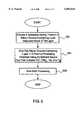
- FIG. 5illustrates, in accordance with one embodiment of the present invention, the steps involved in etching a substrate having thereon an oxide layer disposed above a TiN layer.
- a substrate having thereon an oxide layer disposed above a TiN layeris provided and positioned within the plasma processing chamber.
- the oxide layeris etched using the inventive CO/CHF 3 /neon/N 2 chemistry of the present invention.
- the parameters employed in step 504is substantially similar to those disclosed in Tables 1 and 2. However, the disclosed parameters may be optimized and/or varied to suit the requirements of a particular substrate size, a particular oxide layer (both in composition and in thickness), a particular TiN layer (both in composition and thickness) and/or a specific plasma processing system.
- the substratemay undergo additional processing steps that are conventional in nature. Thereafter, the finished substrate may be processed into dies which may then be made into IC chips or processed to form a flat panel display. The resulting IC chip(s) or flat panel display(s) may then be incorporated into an electronic device, e.g., any of the well known commercial or consumer electronic devices, including digital computers.
- an electronic devicee.g., any of the well known commercial or consumer electronic devices, including digital computers.
- the inventive CO/CHF 3 /neon/N 2 oxide etch chemistryadvantageously yields, in the experiments conducted, a high oxide-to-TiN selectivity relative to prior art C X F Y chemistry.
- Scanning electron microscope (SEM) photographsreveal that the oxide-to-TiN selectivity may be greater than about 50 to 1 or even greater than about 60 to 1. This is a significant improvement over the typical 7 to 1 to 10 to 1 oxide-to-TiN selectivity observed when the prior art C X F Y chemistry is employed.
- the high oxide-to-TiN selectivityis achieved without compromising proper etch profile, critical dimension (CD) control, RIE lag, selectivity to photoresist, and/or residue control.
- the underlying TiN layeris advantageously protected during the oxide etching process due to the high oxide-to-TiN selectivity.
- the high oxide-to-TiN selectivityadvantageously permits a high degree of over-etch during the oxide etch step.
- the ability to perform an extended over-etchis advantageous in etching a multi-level oxide layer since it preserves the TiN material within the via in the thin oxide region while allowing the oxide material in the thick region of the multi-level oxide layer to be completely etched through.
Landscapes
- Engineering & Computer Science (AREA)
- Chemical & Material Sciences (AREA)
- Condensed Matter Physics & Semiconductors (AREA)
- Inorganic Chemistry (AREA)
- Physics & Mathematics (AREA)
- General Chemical & Material Sciences (AREA)
- Chemical Kinetics & Catalysis (AREA)
- General Physics & Mathematics (AREA)
- Manufacturing & Machinery (AREA)
- Computer Hardware Design (AREA)
- Microelectronics & Electronic Packaging (AREA)
- Power Engineering (AREA)
- Drying Of Semiconductors (AREA)
- Internal Circuitry In Semiconductor Integrated Circuit Devices (AREA)
- Storage Of Fruits Or Vegetables (AREA)
Abstract
Description
The present invention relates to the fabrication of semiconductor integrated circuits (IC's) and flat panel displays. More particularly, the present invention relates to improved methods and apparatus for etching through the silicon dioxide-containing layer of a substrate during semiconductor device fabrication.
In the fabrication of semiconductor devices, different layers may be deposited, patterned, and etched to form the desired structures on the substrate (i.e., a glass panel or a semiconductor wafer). In some semiconductor devices, titanium nitride (TiN) is often employed as an etch stop layer during the etching of an overlying silicon dioxide-containing layer or as an antireflective coating (ARC) layer. By way of example, when the TiN layer is employed under a silicon dioxide-containing layer, such as a PETEOS (plasma enhanced tetraethylorthosilicate), BSG (boron-doped silicate glass), USG (undoped silicate glass), BPSG (borophosphosilicate glass), or the like, the TiN material may serve as an etch stop during a via etch through the silicon dioxide-containing layer. Thereafter, the TiN material may serve as a barrier or glue material between the subsequently deposited tungsten or aluminum plugs and any underlying metal layer (e.g., copper or aluminum).
To facilitate discussion, FIG. 1 illustrates a cross section view of some exemplary layers of a substrate. With reference to the figures herein, it should be noted that other additional layers above, below, or between the layers shown may be present. Further, not all of the shown layers need necessarily be present and some or all may be substituted by other different layers. In FIG. 1, there is shown anunderlying layer 102, representing any layer or layers that may underlie a TiN layer on a substrate. For example,underlying layer 102 may represent the substrate itself or may represent layers subsequently deposited and etched prior to the deposition of aTiN layer 104.TiN layer 104 is shown disposed betweenunderlying layer 102 and a subsequently deposited silicon dioxide-containinglayer 106. Although the layers of FIG. 1 have not been shown to scale to facilitate ease of illustration,TiN layer 104 is typically much thinner than silicon dioxide-containinglayer 106.
In some cases, it is often desirable to etch through silicon dioxide-containinglayer 106 down to the interface between silicon dioxide-containinglayer 106 andTiN layer 104 without etching completely throughTiN layer 104. In these cases,TiN layer 104 may function as the etch stop layer, i.e., it is desirable that the etching stops beforeTiN layer 104 is etched through. As semiconductor devices density increases over time, however, it becomes increasingly difficult to etch, using prior art etch techniques, through silicon dioxide-containinglayer 106 without damagingunderlying TiN layer 104. This is because the TiN layer is typically quite thin in modern high density semiconductor devices since a thinner TiN layer is more conducive to the manufacture of high density devices.
In the prior art, the etching of the oxide layer (i.e., the silicon dioxide-containing layer) was typically accomplished using a CX FY chemistry (e.g., CF4, C2 F6, C3 F8, or the like ). The CX FY chemistry was selected primarily for its high etch rate through the oxide layer. By way of example, the prior art CX FY chemistry typically etches through the oxide layer at a rate of greater than about 2,000 angstrom per minute. Unfortunately, the CX FY chemistry has a relatively low selectivity toward TiN. That is, the prior art CX FY chemistry also etches the TiN material at a relatively significant etch rate. For example, the CX FY chemistry typically has an oxide-to-TiN selectivity in the range of 7 to 1 to 10 to 1 (i.e., the CX FY etches through the oxide material 7 to 10 times as fast as it etches through the TiN material).
In FIG. 2, atrench 108 is etched through silicon dioxide-containinglayer 106.TiN layer 104 is intended as the etch stop layer and should have stopped the oxide etch before the oxide etch proceeds through to underlyinglayer 102. Nevertheless, the low TiN selectivity of the prior art chemistry causesTiN layer 104 of FIG. 2, which is quite thin to enable the semiconductor devices to pack closely together, to be completely etched through undertrench 108. When the TiN layer is inadvertently etched through, the bottom oftrench 108 may present an irregular topology to subsequent processes, which may cause the fabricated devices to fail due to, for example, unintended misalignment of layers. Further, the absence of the TiN barrier material at the bottom of the trench may cause ion leakage and/or other unintended electrical characteristics in the fabricated devices. In a typical situation,TiN layer 104 may be etched through either during the main oxide etch step or during the oxide over-etch step.
The low oxide-to-TiN selectivity of the prior art CX FY chemistry also poses significant problems during the etching of multi-level oxide layers. To facilitate discussion, FIG. 3 depicts amulti-level oxide structure 300, including a multilevel oxide layer 302. For illustration purposes,multi-level oxide layer 302 includes athick region 304 and athin region 306 although other regions of various thicknesses may also be present withinmulti-level oxide layer 302.Multi-level oxide layer 302 is disposed onTiN layer 104, which is intended to function as an etch stop during the etching ofmulti-level oxide layer 302. For consistency,underlying layer 102 is also shown disposed belowTiN layer 104.
In some cases, it may be desirable to simultaneously create vias inthick region 304 andthin region 306 ofmulti-level oxide layer 302. Sincethin region 306 is thinner thanthick region 304, via etching inthin region 306 may be completed before the oxide material inthick region 304 is completely etched through. If the oxide etch is allowed to continue to facilitate etching of the via inthick region 304, the low oxide-to-TiN selectivity of the prior art CX FY chemistry may undesirably etch through the TiN material within the via inthin region 306.
On the other hand, if the oxide etch step is shortened to prevent damage to the TiN material underneath the via inthin region 306, the via throughthick region 304 ofmulti-level oxide layer 302 may not be completely etched through. As is apparent, the low oxide-to-TiN selectivity of the prior art chemistry poses serious problems while etching multi-level oxide layers of modern high density ICs.
In view of the foregoing, there are desired improved techniques for etching through the oxide layer during the manufacture of semiconductor devices. The improved techniques preferably provide a high oxide-to-TiN selectivity to substantially reduce damage to the underlying TiN layer during oxide etching.
The invention relates, in one embodiment, to a method for etching a substrate in a plasma processing chamber. The substrate has thereon a silicon dioxide-containing layer disposed above a TiN layer. The method includes positioning the substrate in the plasma processing chamber. There is also included flowing an etchant source gas that includes CO, CHF3, neon and N2 into the plasma processing chamber. Further, there is included forming a plasma out of the etchant source gas within the plasma processing chamber to cause etching of the silicon-dioxide-containing layer.
In another embodiment, the invention relates to a method for preventing damage to an underlying TiN layer while etching a multi-level silicon dioxide-containing layer in a plasma processing chamber. The multi-level silicon dioxide-containing layer is disposed above the TiN layer on a substrate. The multi-level silicon dioxide-containing layer includes a thin region and a thick region. The method includes forming a photoresist mask above the multi-level silicon-dioxide containing layer. The photoresist mask has therein a first via opening above the thin region and a second via opening above the thick region.
The method further includes disposing the substrate, including the photoresist mask, in the plasma processing chamber. There is also included flowing an etchant source gas that includes CO, CHF3, neon and N2 into the plasma processing chamber. Additionally, there is included providing power to electrodes of the plasma processing chamber to form a plasma out of the etchant source gas, thereby causing etching of the multi-level silicon dioxide-containing layer through the first via opening and the second via opening. During etching, the flow rates of the CO, the CHF3, the neon and the N2 are configured to permit the multi-level silicon dioxide-containing layer to be completely etched through in the thick region without damaging the TiN layer under the thin region of the multilevel silicon dioxide-containing layer.
In yet another embodiment, the invention relates to a method for forming an integrated circuit. The method includes providing a semiconductor wafer having thereon a silicon dioxide-containing layer disposed above a TiN layer. There is also included positioning the semiconductor wafer in a plasma processing chamber. Additionally, there is included flowing an etchant source gas that includes CO, CHF3, neon and N2 into the plasma processing chamber. Further, there is included forming a plasma out of the etchant source gas within the plasma processing chamber to cause etching of the silicon-dioxide-containing layer.
These and other features of the present invention will be described in more detail below in the detailed description of the invention and in conjunction with the following figures.
The present invention is illustrated by way of example, and not by way of limitation, in the figures of the accompanying drawings and in which like reference numerals refer to similar elements and in which:
To facilitate discussion, FIG. 1 illustrates a cross section view of some exemplary layers of a substrate, including the silicon dioxide-containing layer and the underlying TiN layer.
In FIG. 2, a trench is etched through silicon dioxide-containing layer of FIG. 1.
FIG. 3 depicts an exemplary multi-level oxide structure, including a multi level oxide layer.
FIG. 4 illustrates a triode-type plasma processing system, representing a plasma processing system suitable for use with the inventive CO/CHF3 /neon/N2 oxide etch technique.
FIG. 5 illustrates, in accordance with one embodiment of the present invention, the steps involved in etching a substrate having thereon an oxide layer disposed above a TiN layer.
The present invention will now be described in detail with reference to a few preferred embodiments thereof as illustrated in the accompanying drawings. In the following description, numerous specific details are set forth in order to provide a thorough understanding of the present invention. It will be apparent, however, to one skilled in the art, that the present invention may be practiced without some or all of these specific details. In other instances, well known process steps and/or structures have not been described in detail in order to not unnecessarily obscure the present invention.
In accordance with one aspect of the present invention, the aforementioned TiN damage issue is substantially alleviated by etching the oxide layer (i.e., the silicon dioxide-containing layer) with a novel chemistry that includes CO, CHF3, neon and N2 in a plasma processing system. In a preferred embodiment, the inventive chemistry is employed to etch through the oxide layer in a triode-type plasma processing system such as the Lam 9500™ plasma processing system available from Lam Research Corp. of Fremont, Calif. However, it is contemplated that the inventive oxide etch technique, using the inventive CO/CHF3 /neon/N2 chemistry, may be performed in any of the known plasma processing apparatuses including, but not limited to, those adapted for dry etching, plasma etching, reactive ion etching, magnetically enhanced reactive ion etching, electron cyclotron resonance etching, or the like. Note that the this is true irrespective of whether energy to the plasma is delivered through capacitively coupled parallel electrode plates, through ECR microwave plasma sources, or through inductively coupled RF sources such as helicon, helical resonators, and transformer coupled sources (either planar or non-planar). These processing systems, among others, are readily available commercially from a number of vendors including the aforementioned Lam Research Corp.
To facilitate discussion, FIG. 4 illustrates a triode-typeplasma processing system 402, representing a plasma processing system suitable for use with the inventive CO/CHF3 /neon/N2 oxide etch technique. Referring now to FIG. 4, triode-typeplasma processing system 402 includes achamber 404. Withinchamber 404, there is disposed anupper electrode 406 and alower electrode 408. In the embodiment of FIG. 4,upper electrode 406 represents a combination electrode/gas distribution plate mechanism through which etchant source gases entering throughport 410 is distributed intochamber 404 throughapertures 412.
Abovelower electrode 408, there is disposed asubstrate 414, representing, for example, a glass panel or a semiconductor wafer having thereon an oxide layer to be etched.Upper electrode 406 andlower electrode 408 are powered by anRF power source 420, which provides radio frequency (RF) power to the electrodes via appropriate matching and/or capacitive blocking networks (conventional and not shown to simplify the illustration). In one embodiment, the frequency range ofRF power source 420 is about 13.56 MEz although other suitable RF frequency ranges may also be employed.
Betweenupper electrode 406 andsubstrate 414, there is disposed a groundedanode 422. In embodiment of FIG. 4, groundedanode 422 represents a grounded hollow anode, i.e., a grounded grid having therein a plurality of apertures or aberrations. During plasma etching, groundedanode 422 helps improve the etch uniformity onsubstrate 414 by more uniformly distributing the ions over the surface ofsubstrate 414.
To prepare for oxide etching,substrate 414 having thereon an oxide layer disposed above a TiN layer is introduced intochamber 404 and positioned on top oflower electrode 408. The inventive CO/C HF3 /Neon/N2 etchant source gas is then flowed throughport 410. When RF power is supplied toupper electrode 406 andlower electrode 408, aremote plasma cloud 416 is struck in betweenupper electrode 406 and the groundedanode 422, and a reactive ion etching (RIE)plasma cloud 418 is ignited within the region between groundedanode 422 andsubstrate 414 to etch the exposed surface ofsubstrate 414. The reaction creates volatile byproducts, which are then exhausted away throughexhaust port 450. The oxide etch step ends after a predetermined time has elapsed or when an appropriate monitoring apparatus (such as an optical wavelength monitor) detects that the oxide material has been etched through.
While not wishing to be bound by theory, it is believed that the formation of titanium oxide over the TiN surface contributes to the high oxide-to-TiN selectivity of the inventive CO/CHF3 /Neon/N2 oxide etching technique. The titanium oxide is believed to be formed as CO reacts with TiN. Alternatively or additionally, it is believed that the reactions between CHF3, CO2, COF2 and SiF4 generate CF2, CFX, and CHFX polymers. Some of the polymers formed (believed to be fluorocarbon or hydrofluorocarbon) may block the etching of the underlying TiN layer during oxide etching. When so blocked, TiN erosion is retarded to a significant degree. Alternatively or additionally, it is believed that as the oxide material is removed in the via and the TiN material is exposed to the reactive species, titanium will be sputtered onto the side walls of the via and catalyze the formation of polymer to block TiN etching. Alternatively or additionally, neon is believed to play a role in controlling the RIE lag (i.e., reducing the disparity in the etch rate in the open region of the substrate versus the etch rate in the narrow region). N2 is believed to help remove polymer residues and is also believed to play a role in RIE lag control.
In one example, an 8-inch wafer having thereon a 600 angstroms thick layer of TiN and a multi-level PETEOS layer of 7,000 angstroms thick and 14,000 angstroms thick is disposed in the aforementioned Lam 6500™ plasma processing system. Table 1 illustrates the approximate parameters for use in the oxide main etch step while etching through the oxide layer on the sample wafer.
TABLE 1 ______________________________________ Suitable Preferred Preferred Range Range Value ______________________________________ Time 80-120 90-110 100 (seconds) CHF.sub.3 flow 35-65 45-55 50 (sccm) CO flow 25-45 30-40 35 (sccm) Neon flow 180-220 190-210 200 (sccm) N.sub.2 flow 20-40 25-35 30 (sccm) Upper 15-25 18-22 20 Electrode Temp (° C.) Lower 8-16 10-14 12 Electrode Temp (° C.) Power 400-700 500-600 550 (Watts) Pressure 125-175 140-160 150 (mTorr) ______________________________________
Table 2 illustrates the approximate parameters for use in the oxide over-etch step while etching through the oxide layer on the sample wafer.
TABLE 2 ______________________________________ Suitable Preferred Preferred Range Range Value ______________________________________ Time 80-120 90-110 100 (seconds) CHF.sub.3 flow 20-40 25-35 30 (sccm) CO flow 40-70 50-60 55 (sccm) Neonflow 180-220 190-210 200 (sccm) N.sub.2 flow 20-40 25-35 30 (sccm) Upper 15-25 18-22 20 Electrode Temp (° C.) Lower 8-16 10-14 12 Electrode Temp (° C.) Power 400-700 500-600 550 (Watts) Pressure 125-175 140-160 150 (mTorr) ______________________________________
FIG. 5 illustrates, in accordance with one embodiment of the present invention, the steps involved in etching a substrate having thereon an oxide layer disposed above a TiN layer. Instep 502, a substrate having thereon an oxide layer disposed above a TiN layer is provided and positioned within the plasma processing chamber. Instep 504, the oxide layer is etched using the inventive CO/CHF3 /neon/N2 chemistry of the present invention. In one embodiment, the parameters employed instep 504 is substantially similar to those disclosed in Tables 1 and 2. However, the disclosed parameters may be optimized and/or varied to suit the requirements of a particular substrate size, a particular oxide layer (both in composition and in thickness), a particular TiN layer (both in composition and thickness) and/or a specific plasma processing system.
Instep 506, the substrate may undergo additional processing steps that are conventional in nature. Thereafter, the finished substrate may be processed into dies which may then be made into IC chips or processed to form a flat panel display. The resulting IC chip(s) or flat panel display(s) may then be incorporated into an electronic device, e.g., any of the well known commercial or consumer electronic devices, including digital computers.
The inventive CO/CHF3 /neon/N2 oxide etch chemistry advantageously yields, in the experiments conducted, a high oxide-to-TiN selectivity relative to prior art CX FY chemistry. Scanning electron microscope (SEM) photographs reveal that the oxide-to-TiN selectivity may be greater than about 50 to 1 or even greater than about 60 to 1. This is a significant improvement over the typical 7 to 1 to 10 to 1 oxide-to-TiN selectivity observed when the prior art CX FY chemistry is employed.
Further, analysis of SEM photographs reveals that the high oxide-to-TiN selectivity is achieved without compromising proper etch profile, critical dimension (CD) control, RIE lag, selectivity to photoresist, and/or residue control. As can be appreciated by those skilled in the art, the underlying TiN layer is advantageously protected during the oxide etching process due to the high oxide-to-TiN selectivity. Further, the high oxide-to-TiN selectivity advantageously permits a high degree of over-etch during the oxide etch step. The ability to perform an extended over-etch is advantageous in etching a multi-level oxide layer since it preserves the TiN material within the via in the thin oxide region while allowing the oxide material in the thick region of the multi-level oxide layer to be completely etched through.
While this invention has been described in terms of several preferred embodiments, there are alterations, permutations, and equivalents which fall within the scope of this invention. It should also be noted that there are may alternative ways of implementing the methods and apparatuses of the present invention. It is therefore intended that the following appended claims be interpreted as including all such alterations, permutations, and equivalents as fall within the true spirit and scope of the present invention.
Claims (34)
1. A method for etching a substrate in a plasma processing chamber and providing a high oxide-to-TiN selectivity, said substrate having thereon a silicon dioxide-containing layer disposed above a TiN layer, said method comprising:
positioning said substrate in said plasma processing chamber;
flowing an echant source gas that includes CO, CHF3, neon and N2 into said plasma processing chamber, whereby a layer of titanium oxide is formed over the surface of the TiN layer by the reaction of the CO with the TiN, the titanium oxide contributing to the high oxide-to-TiN selectivity in association with the etchant source gas; and
forming a plasma out of said etchant source gas within said plasma processing chamber to cause etching of said silicon-dioxide-containing layer.
2. The method of claim 1 wherein said substrate is a semiconductor wafer.
3. The method of claim 1 wherein said substrate is a glass panel.
4. The method of claim 1 wherein said silicon dioxide-containing layer represents a tetraethylorthosilicate (TEOS) layer.
5. The method of claim 1 wherein said etchant source gas consists essentially of CO, CHF3, neon and N2.
6. The method of claim 5 wherein a flow ratio of said CHF3 to said CO is about 1.1 to 1.8.
7. The method of claim 5 wherein a flow ratio of said CHF3 to said neon is about 0.2 to 0.3.
8. The method of claim 5 wherein a flow ratio of said CHF3 to said N2 is about 1.5 to 2.0.
9. The method of claim 5 wherein said plasma processing chamber represents a triode-type plasma processing chamber having therein a grounded hollow anode.
10. The method of claim 1 wherein said substrate represents a substrate for forming integrated circuits (ICs).
11. The method of claim 1, wherein the reactions between the CO, CHF3, neon and N2 generate CF2, CFx, and CHFx polymers.
12. The method of claim 11, wherein the polymers formed include fluorocarbon or hydrofluorocarbon.
13. The method of claim 11, wherein the polymers block the etching of the underlying TiN layer during oxide etching.
14. The method of claim 1, wherein as the oxide material is removed in a via and the TiN material is exposed to a reactive species, titanium is sputtered onto the side walls of the via and serves to catalyze the formation of polymer-to-TiN etching.
15. A method for preventing damage to an underlying TiN layer while etching a multi-level silicon dioxide-containing layer in a plasma processing chamber and providing a high oxide-to-TiN selectivity, said multi-level silicon dioxide-containing layer being disposed above said TiN layer on a substrate, said multi-level silicon dioxide-containing layer including a thin region and a thick region, said method comprising:
forming a photoresist mask above said multi-level silicon-dioxide containing layer, said photoresist mask having therein a first via opening above said thin region and a second via opening above said thick region;
disposing said substrate, including said photoresist mask, in said plasma processing chamber;
flowing an etchant source gas that includes CO, CHF3, neon and N2 into said plasma processing chamber, whereby a layer of titanium oxide is formed over the surface of the TiN layer by the reaction of the CO with the TiN, the titanium oxide contributing to the high oxide-to-TiN selectivity in association with the etchant source gas; and
providing power to electrodes of said plasma processing chamber to form a plasma out of said etchant source gas, thereby causing etching of said multi-level silicon dioxide-containing layer through said first via opening and said second via opening, flow rates of said CO, said CHF3, said neon and said N2 being configured permit said multi-level silicon dioxide-containing layer to be completely etched through in said thick region without damaging said TiN layer under said thin region of said multi-level silicon dioxide-containing layer.
16. The method of claim 15 wherein said etchant source gas consists essentially of CO, CHF3, neon and N2.
17. The method of claim 16 wherein a flow ratio of said CHF3 to said CO is about 0.4 to 0.6.
18. The method of claim 16 wherein a flow ratio of said CHF3 to said neon is about 0.1 to 0.2.
19. The method of claim 16 wherein a flow ratio of said CHF3 to said N2 is about 0.8 to 1.4.
20. The method of claim 16 wherein said plasma processing chamber represents a triode-type plasma processing chamber having therein a grounded hollow anode.
21. The method of claim 15 wherein said substrate is a semiconductor wafer.
22. The method of claim 15 wherein said silicon dioxide-containing layer represents a tetraethylorthosilicate (TEOS) layer.
23. The method of claim 15 wherein said substrate represents a substrate for forming integrated circuits (ICs).
24. The method of claim 15 wherein said substrate represents a substrate for forming a flat panel display.
25. The method of claim 15, wherein the reactions between the CO, CHF3, neon and N2 generate CF2, CFx, and CHFx polymers.
26. The method of claim 25, wherein the polymers formed include fluorocarbon or hydrofluorocarbon.
27. The method of claim 25, wherein the polymers block the etching of the underlying TiN layer during oxide etching.
28. The method of claim 15, wherein as the oxide material is removed in a via and the TiN material is exposed to a reactive species, titanium is sputtered onto the side walls of the via and serves to catalyze the formation of polymer-to-TiN etching.
29. A method for forming an integrated circuit, comprising:
providing a semiconductor wafer having thereon a silicon dioxide-containing layer disposed above a TiN layer;
positioning said semiconductor wafer in a plasma processing chamber;
flowing an etchant source gas that includes CO, CHF3, neon and N2 into said plasma processing chamber, whereby a layer of titanium oxide is formed over the surface of the TiN layer by the reaction of the CO with the TiN, the titanium oxide contributing to a high oxide-to-TiN selectivity in association with the etchant source gas; and
forming a plasma out of said etchant source gas within said plasma processing chamber to cause etching of said silicon-dioxide-containing layer.
30. The method of claim 29 wherein said etchant source gas consists essentially of CO, CHF3, neon and N2.
31. The method of claim 29, wherein the reactions between the CO, CHF3, neon and N2 generate CF2, CFx, and CHFx polymers.
32. The method of claim 31, wherein the polymers formed include fluorocarbon or hydrofluorocarbon.
33. The method of claim 31, wherein the polymers block the etching of the underlying TiN layer during oxide etching.
34. The method of claim 29, wherein as the oxide material is removed in a via and the TiN material is exposed to a reactive species, titanium is sputtered onto the side walls of the via and serves to catalyze the formation of polymer-to-TiN etching.
Priority Applications (7)
| Application Number | Priority Date | Filing Date | Title |
|---|---|---|---|
| US08/996,071US6083844A (en) | 1997-12-22 | 1997-12-22 | Techniques for etching an oxide layer |
| JP2000525913AJP4454148B2 (en) | 1997-12-22 | 1998-12-11 | Improved oxide layer etching method |
| PCT/US1998/026499WO1999033097A1 (en) | 1997-12-22 | 1998-12-11 | Improved techniques for etching an oxide layer |
| AT98963140TATE331298T1 (en) | 1997-12-22 | 1998-12-11 | IMPROVED METHOD OF ETCHING AN OXIDE LAYER |
| EP98963140AEP1042796B1 (en) | 1997-12-22 | 1998-12-11 | Improved techniques for etching an oxide layer |
| DE69835032TDE69835032T2 (en) | 1997-12-22 | 1998-12-11 | IMPROVED METHOD TO EAT AN OXIDE LAYER |
| TW087120755ATW446757B (en) | 1997-12-22 | 1998-12-14 | Improved techniques for etching an oxide layer |
Applications Claiming Priority (1)
| Application Number | Priority Date | Filing Date | Title |
|---|---|---|---|
| US08/996,071US6083844A (en) | 1997-12-22 | 1997-12-22 | Techniques for etching an oxide layer |
Publications (1)
| Publication Number | Publication Date |
|---|---|
| US6083844Atrue US6083844A (en) | 2000-07-04 |
Family
ID=25542474
Family Applications (1)
| Application Number | Title | Priority Date | Filing Date |
|---|---|---|---|
| US08/996,071Expired - LifetimeUS6083844A (en) | 1997-12-22 | 1997-12-22 | Techniques for etching an oxide layer |
Country Status (7)
| Country | Link |
|---|---|
| US (1) | US6083844A (en) |
| EP (1) | EP1042796B1 (en) |
| JP (1) | JP4454148B2 (en) |
| AT (1) | ATE331298T1 (en) |
| DE (1) | DE69835032T2 (en) |
| TW (1) | TW446757B (en) |
| WO (1) | WO1999033097A1 (en) |
Cited By (150)
| Publication number | Priority date | Publication date | Assignee | Title |
|---|---|---|---|---|
| US6217786B1 (en)* | 1998-12-31 | 2001-04-17 | Lam Research Corporation | Mechanism for bow reduction and critical dimension control in etching silicon dioxide using hydrogen-containing additive gases in fluorocarbon gas chemistry |
| US6376382B1 (en)* | 1998-11-27 | 2002-04-23 | United Microelectronics Corp. | Method for forming an opening |
| US6486070B1 (en) | 2000-09-21 | 2002-11-26 | Lam Research Corporation | Ultra-high oxide to photoresist selective etch of high-aspect-ratio openings in a low-pressure, high-density plasma |
| US20030064601A1 (en)* | 2001-09-28 | 2003-04-03 | Thompson Keith J. | Method for via etching in organo-silica-glass |
| US20050056875A1 (en)* | 1999-04-15 | 2005-03-17 | Li Li | Method of plasma etching a substrate |
| US6949469B1 (en) | 2003-12-16 | 2005-09-27 | Lam Research Corporation | Methods and apparatus for the optimization of photo resist etching in a plasma processing system |
| US8921234B2 (en)* | 2012-12-21 | 2014-12-30 | Applied Materials, Inc. | Selective titanium nitride etching |
| US9012302B2 (en) | 2011-09-26 | 2015-04-21 | Applied Materials, Inc. | Intrench profile |
| US9117855B2 (en) | 2013-12-04 | 2015-08-25 | Applied Materials, Inc. | Polarity control for remote plasma |
| US9132436B2 (en) | 2012-09-21 | 2015-09-15 | Applied Materials, Inc. | Chemical control features in wafer process equipment |
| US9136273B1 (en) | 2014-03-21 | 2015-09-15 | Applied Materials, Inc. | Flash gate air gap |
| US9153442B2 (en) | 2013-03-15 | 2015-10-06 | Applied Materials, Inc. | Processing systems and methods for halide scavenging |
| US9159606B1 (en) | 2014-07-31 | 2015-10-13 | Applied Materials, Inc. | Metal air gap |
| US9165786B1 (en) | 2014-08-05 | 2015-10-20 | Applied Materials, Inc. | Integrated oxide and nitride recess for better channel contact in 3D architectures |
| US9190293B2 (en) | 2013-12-18 | 2015-11-17 | Applied Materials, Inc. | Even tungsten etch for high aspect ratio trenches |
| US9209012B2 (en) | 2013-09-16 | 2015-12-08 | Applied Materials, Inc. | Selective etch of silicon nitride |
| US9236265B2 (en) | 2013-11-04 | 2016-01-12 | Applied Materials, Inc. | Silicon germanium processing |
| US9236266B2 (en) | 2011-08-01 | 2016-01-12 | Applied Materials, Inc. | Dry-etch for silicon-and-carbon-containing films |
| US9245762B2 (en) | 2013-12-02 | 2016-01-26 | Applied Materials, Inc. | Procedure for etch rate consistency |
| US9263278B2 (en) | 2013-12-17 | 2016-02-16 | Applied Materials, Inc. | Dopant etch selectivity control |
| US9269590B2 (en) | 2014-04-07 | 2016-02-23 | Applied Materials, Inc. | Spacer formation |
| US9287134B2 (en) | 2014-01-17 | 2016-03-15 | Applied Materials, Inc. | Titanium oxide etch |
| US9287095B2 (en) | 2013-12-17 | 2016-03-15 | Applied Materials, Inc. | Semiconductor system assemblies and methods of operation |
| US9293568B2 (en) | 2014-01-27 | 2016-03-22 | Applied Materials, Inc. | Method of fin patterning |
| US9299538B2 (en) | 2014-03-20 | 2016-03-29 | Applied Materials, Inc. | Radial waveguide systems and methods for post-match control of microwaves |
| US9299575B2 (en) | 2014-03-17 | 2016-03-29 | Applied Materials, Inc. | Gas-phase tungsten etch |
| US9299582B2 (en) | 2013-11-12 | 2016-03-29 | Applied Materials, Inc. | Selective etch for metal-containing materials |
| US9299583B1 (en) | 2014-12-05 | 2016-03-29 | Applied Materials, Inc. | Aluminum oxide selective etch |
| US9299537B2 (en) | 2014-03-20 | 2016-03-29 | Applied Materials, Inc. | Radial waveguide systems and methods for post-match control of microwaves |
| US9309598B2 (en) | 2014-05-28 | 2016-04-12 | Applied Materials, Inc. | Oxide and metal removal |
| US9324576B2 (en) | 2010-05-27 | 2016-04-26 | Applied Materials, Inc. | Selective etch for silicon films |
| US9343272B1 (en) | 2015-01-08 | 2016-05-17 | Applied Materials, Inc. | Self-aligned process |
| US9349605B1 (en) | 2015-08-07 | 2016-05-24 | Applied Materials, Inc. | Oxide etch selectivity systems and methods |
| US9355862B2 (en) | 2014-09-24 | 2016-05-31 | Applied Materials, Inc. | Fluorine-based hardmask removal |
| US9355863B2 (en) | 2012-12-18 | 2016-05-31 | Applied Materials, Inc. | Non-local plasma oxide etch |
| US9355856B2 (en) | 2014-09-12 | 2016-05-31 | Applied Materials, Inc. | V trench dry etch |
| US9362130B2 (en) | 2013-03-01 | 2016-06-07 | Applied Materials, Inc. | Enhanced etching processes using remote plasma sources |
| US9368364B2 (en) | 2014-09-24 | 2016-06-14 | Applied Materials, Inc. | Silicon etch process with tunable selectivity to SiO2 and other materials |
| US9373517B2 (en) | 2012-08-02 | 2016-06-21 | Applied Materials, Inc. | Semiconductor processing with DC assisted RF power for improved control |
| US9373522B1 (en) | 2015-01-22 | 2016-06-21 | Applied Mateials, Inc. | Titanium nitride removal |
| US9378969B2 (en) | 2014-06-19 | 2016-06-28 | Applied Materials, Inc. | Low temperature gas-phase carbon removal |
| US9378978B2 (en) | 2014-07-31 | 2016-06-28 | Applied Materials, Inc. | Integrated oxide recess and floating gate fin trimming |
| US9385028B2 (en) | 2014-02-03 | 2016-07-05 | Applied Materials, Inc. | Air gap process |
| US9384997B2 (en) | 2012-11-20 | 2016-07-05 | Applied Materials, Inc. | Dry-etch selectivity |
| US9390937B2 (en) | 2012-09-20 | 2016-07-12 | Applied Materials, Inc. | Silicon-carbon-nitride selective etch |
| US9396989B2 (en) | 2014-01-27 | 2016-07-19 | Applied Materials, Inc. | Air gaps between copper lines |
| US9406523B2 (en) | 2014-06-19 | 2016-08-02 | Applied Materials, Inc. | Highly selective doped oxide removal method |
| US9412608B2 (en) | 2012-11-30 | 2016-08-09 | Applied Materials, Inc. | Dry-etch for selective tungsten removal |
| US9418858B2 (en) | 2011-10-07 | 2016-08-16 | Applied Materials, Inc. | Selective etch of silicon by way of metastable hydrogen termination |
| US9425058B2 (en) | 2014-07-24 | 2016-08-23 | Applied Materials, Inc. | Simplified litho-etch-litho-etch process |
| US9437451B2 (en) | 2012-09-18 | 2016-09-06 | Applied Materials, Inc. | Radical-component oxide etch |
| US9449846B2 (en) | 2015-01-28 | 2016-09-20 | Applied Materials, Inc. | Vertical gate separation |
| US9478432B2 (en) | 2014-09-25 | 2016-10-25 | Applied Materials, Inc. | Silicon oxide selective removal |
| US9496167B2 (en) | 2014-07-31 | 2016-11-15 | Applied Materials, Inc. | Integrated bit-line airgap formation and gate stack post clean |
| US9493879B2 (en) | 2013-07-12 | 2016-11-15 | Applied Materials, Inc. | Selective sputtering for pattern transfer |
| US9499898B2 (en) | 2014-03-03 | 2016-11-22 | Applied Materials, Inc. | Layered thin film heater and method of fabrication |
| US9502258B2 (en) | 2014-12-23 | 2016-11-22 | Applied Materials, Inc. | Anisotropic gap etch |
| US9553102B2 (en) | 2014-08-19 | 2017-01-24 | Applied Materials, Inc. | Tungsten separation |
| US9576809B2 (en) | 2013-11-04 | 2017-02-21 | Applied Materials, Inc. | Etch suppression with germanium |
| US9607856B2 (en) | 2013-03-05 | 2017-03-28 | Applied Materials, Inc. | Selective titanium nitride removal |
| US9659753B2 (en) | 2014-08-07 | 2017-05-23 | Applied Materials, Inc. | Grooved insulator to reduce leakage current |
| US9691645B2 (en) | 2015-08-06 | 2017-06-27 | Applied Materials, Inc. | Bolted wafer chuck thermal management systems and methods for wafer processing systems |
| US9721789B1 (en) | 2016-10-04 | 2017-08-01 | Applied Materials, Inc. | Saving ion-damaged spacers |
| US9728437B2 (en) | 2015-02-03 | 2017-08-08 | Applied Materials, Inc. | High temperature chuck for plasma processing systems |
| US9741593B2 (en) | 2015-08-06 | 2017-08-22 | Applied Materials, Inc. | Thermal management systems and methods for wafer processing systems |
| US9768034B1 (en) | 2016-11-11 | 2017-09-19 | Applied Materials, Inc. | Removal methods for high aspect ratio structures |
| US9773648B2 (en) | 2013-08-30 | 2017-09-26 | Applied Materials, Inc. | Dual discharge modes operation for remote plasma |
| US9842744B2 (en) | 2011-03-14 | 2017-12-12 | Applied Materials, Inc. | Methods for etch of SiN films |
| US9847289B2 (en) | 2014-05-30 | 2017-12-19 | Applied Materials, Inc. | Protective via cap for improved interconnect performance |
| US9865484B1 (en) | 2016-06-29 | 2018-01-09 | Applied Materials, Inc. | Selective etch using material modification and RF pulsing |
| US9881805B2 (en) | 2015-03-02 | 2018-01-30 | Applied Materials, Inc. | Silicon selective removal |
| US9887096B2 (en) | 2012-09-17 | 2018-02-06 | Applied Materials, Inc. | Differential silicon oxide etch |
| US9885117B2 (en) | 2014-03-31 | 2018-02-06 | Applied Materials, Inc. | Conditioned semiconductor system parts |
| US9934942B1 (en) | 2016-10-04 | 2018-04-03 | Applied Materials, Inc. | Chamber with flow-through source |
| US9947549B1 (en) | 2016-10-10 | 2018-04-17 | Applied Materials, Inc. | Cobalt-containing material removal |
| US10026621B2 (en) | 2016-11-14 | 2018-07-17 | Applied Materials, Inc. | SiN spacer profile patterning |
| US10043674B1 (en) | 2017-08-04 | 2018-08-07 | Applied Materials, Inc. | Germanium etching systems and methods |
| US10043684B1 (en) | 2017-02-06 | 2018-08-07 | Applied Materials, Inc. | Self-limiting atomic thermal etching systems and methods |
| US10049891B1 (en) | 2017-05-31 | 2018-08-14 | Applied Materials, Inc. | Selective in situ cobalt residue removal |
| US10062578B2 (en) | 2011-03-14 | 2018-08-28 | Applied Materials, Inc. | Methods for etch of metal and metal-oxide films |
| US10062587B2 (en) | 2012-07-18 | 2018-08-28 | Applied Materials, Inc. | Pedestal with multi-zone temperature control and multiple purge capabilities |
| US10062575B2 (en) | 2016-09-09 | 2018-08-28 | Applied Materials, Inc. | Poly directional etch by oxidation |
| US10062585B2 (en) | 2016-10-04 | 2018-08-28 | Applied Materials, Inc. | Oxygen compatible plasma source |
| US10062579B2 (en) | 2016-10-07 | 2018-08-28 | Applied Materials, Inc. | Selective SiN lateral recess |
| US10128086B1 (en) | 2017-10-24 | 2018-11-13 | Applied Materials, Inc. | Silicon pretreatment for nitride removal |
| US10163696B2 (en) | 2016-11-11 | 2018-12-25 | Applied Materials, Inc. | Selective cobalt removal for bottom up gapfill |
| US10170282B2 (en) | 2013-03-08 | 2019-01-01 | Applied Materials, Inc. | Insulated semiconductor faceplate designs |
| US10170336B1 (en) | 2017-08-04 | 2019-01-01 | Applied Materials, Inc. | Methods for anisotropic control of selective silicon removal |
| US10224210B2 (en) | 2014-12-09 | 2019-03-05 | Applied Materials, Inc. | Plasma processing system with direct outlet toroidal plasma source |
| US10242908B2 (en) | 2016-11-14 | 2019-03-26 | Applied Materials, Inc. | Airgap formation with damage-free copper |
| US10256112B1 (en) | 2017-12-08 | 2019-04-09 | Applied Materials, Inc. | Selective tungsten removal |
| US10283324B1 (en) | 2017-10-24 | 2019-05-07 | Applied Materials, Inc. | Oxygen treatment for nitride etching |
| US10283321B2 (en) | 2011-01-18 | 2019-05-07 | Applied Materials, Inc. | Semiconductor processing system and methods using capacitively coupled plasma |
| US10297458B2 (en) | 2017-08-07 | 2019-05-21 | Applied Materials, Inc. | Process window widening using coated parts in plasma etch processes |
| US10319600B1 (en) | 2018-03-12 | 2019-06-11 | Applied Materials, Inc. | Thermal silicon etch |
| US10319739B2 (en) | 2017-02-08 | 2019-06-11 | Applied Materials, Inc. | Accommodating imperfectly aligned memory holes |
| US10319649B2 (en) | 2017-04-11 | 2019-06-11 | Applied Materials, Inc. | Optical emission spectroscopy (OES) for remote plasma monitoring |
| US10354889B2 (en) | 2017-07-17 | 2019-07-16 | Applied Materials, Inc. | Non-halogen etching of silicon-containing materials |
| US10403507B2 (en) | 2017-02-03 | 2019-09-03 | Applied Materials, Inc. | Shaped etch profile with oxidation |
| US10431429B2 (en) | 2017-02-03 | 2019-10-01 | Applied Materials, Inc. | Systems and methods for radial and azimuthal control of plasma uniformity |
| US10468267B2 (en) | 2017-05-31 | 2019-11-05 | Applied Materials, Inc. | Water-free etching methods |
| US10490418B2 (en) | 2014-10-14 | 2019-11-26 | Applied Materials, Inc. | Systems and methods for internal surface conditioning assessment in plasma processing equipment |
| US10490406B2 (en) | 2018-04-10 | 2019-11-26 | Appled Materials, Inc. | Systems and methods for material breakthrough |
| US10497573B2 (en) | 2018-03-13 | 2019-12-03 | Applied Materials, Inc. | Selective atomic layer etching of semiconductor materials |
| US10504754B2 (en) | 2016-05-19 | 2019-12-10 | Applied Materials, Inc. | Systems and methods for improved semiconductor etching and component protection |
| US10504700B2 (en) | 2015-08-27 | 2019-12-10 | Applied Materials, Inc. | Plasma etching systems and methods with secondary plasma injection |
| US10522371B2 (en) | 2016-05-19 | 2019-12-31 | Applied Materials, Inc. | Systems and methods for improved semiconductor etching and component protection |
| US10541184B2 (en) | 2017-07-11 | 2020-01-21 | Applied Materials, Inc. | Optical emission spectroscopic techniques for monitoring etching |
| US10541246B2 (en) | 2017-06-26 | 2020-01-21 | Applied Materials, Inc. | 3D flash memory cells which discourage cross-cell electrical tunneling |
| US10546729B2 (en) | 2016-10-04 | 2020-01-28 | Applied Materials, Inc. | Dual-channel showerhead with improved profile |
| US10566206B2 (en) | 2016-12-27 | 2020-02-18 | Applied Materials, Inc. | Systems and methods for anisotropic material breakthrough |
| US10573527B2 (en) | 2018-04-06 | 2020-02-25 | Applied Materials, Inc. | Gas-phase selective etching systems and methods |
| US10573496B2 (en) | 2014-12-09 | 2020-02-25 | Applied Materials, Inc. | Direct outlet toroidal plasma source |
| US10593523B2 (en) | 2014-10-14 | 2020-03-17 | Applied Materials, Inc. | Systems and methods for internal surface conditioning in plasma processing equipment |
| US10593560B2 (en) | 2018-03-01 | 2020-03-17 | Applied Materials, Inc. | Magnetic induction plasma source for semiconductor processes and equipment |
| US10615047B2 (en) | 2018-02-28 | 2020-04-07 | Applied Materials, Inc. | Systems and methods to form airgaps |
| US10629473B2 (en) | 2016-09-09 | 2020-04-21 | Applied Materials, Inc. | Footing removal for nitride spacer |
| US10672642B2 (en) | 2018-07-24 | 2020-06-02 | Applied Materials, Inc. | Systems and methods for pedestal configuration |
| US10679870B2 (en) | 2018-02-15 | 2020-06-09 | Applied Materials, Inc. | Semiconductor processing chamber multistage mixing apparatus |
| US10699879B2 (en) | 2018-04-17 | 2020-06-30 | Applied Materials, Inc. | Two piece electrode assembly with gap for plasma control |
| US10727080B2 (en) | 2017-07-07 | 2020-07-28 | Applied Materials, Inc. | Tantalum-containing material removal |
| US10755941B2 (en) | 2018-07-06 | 2020-08-25 | Applied Materials, Inc. | Self-limiting selective etching systems and methods |
| CN111886689A (en)* | 2018-03-19 | 2020-11-03 | 朗姆研究公司 | Non-chamfer through hole integration scheme |
| US10854426B2 (en) | 2018-01-08 | 2020-12-01 | Applied Materials, Inc. | Metal recess for semiconductor structures |
| US10872778B2 (en) | 2018-07-06 | 2020-12-22 | Applied Materials, Inc. | Systems and methods utilizing solid-phase etchants |
| US10886137B2 (en) | 2018-04-30 | 2021-01-05 | Applied Materials, Inc. | Selective nitride removal |
| US10892198B2 (en) | 2018-09-14 | 2021-01-12 | Applied Materials, Inc. | Systems and methods for improved performance in semiconductor processing |
| US10903054B2 (en) | 2017-12-19 | 2021-01-26 | Applied Materials, Inc. | Multi-zone gas distribution systems and methods |
| US10920319B2 (en) | 2019-01-11 | 2021-02-16 | Applied Materials, Inc. | Ceramic showerheads with conductive electrodes |
| US10920320B2 (en) | 2017-06-16 | 2021-02-16 | Applied Materials, Inc. | Plasma health determination in semiconductor substrate processing reactors |
| US10943834B2 (en) | 2017-03-13 | 2021-03-09 | Applied Materials, Inc. | Replacement contact process |
| US10964512B2 (en) | 2018-02-15 | 2021-03-30 | Applied Materials, Inc. | Semiconductor processing chamber multistage mixing apparatus and methods |
| US11024486B2 (en) | 2013-02-08 | 2021-06-01 | Applied Materials, Inc. | Semiconductor processing systems having multiple plasma configurations |
| US11049755B2 (en) | 2018-09-14 | 2021-06-29 | Applied Materials, Inc. | Semiconductor substrate supports with embedded RF shield |
| US11062887B2 (en) | 2018-09-17 | 2021-07-13 | Applied Materials, Inc. | High temperature RF heater pedestals |
| US11121002B2 (en) | 2018-10-24 | 2021-09-14 | Applied Materials, Inc. | Systems and methods for etching metals and metal derivatives |
| US11239061B2 (en) | 2014-11-26 | 2022-02-01 | Applied Materials, Inc. | Methods and systems to enhance process uniformity |
| US11257693B2 (en) | 2015-01-09 | 2022-02-22 | Applied Materials, Inc. | Methods and systems to improve pedestal temperature control |
| US11276559B2 (en) | 2017-05-17 | 2022-03-15 | Applied Materials, Inc. | Semiconductor processing chamber for multiple precursor flow |
| US11276590B2 (en) | 2017-05-17 | 2022-03-15 | Applied Materials, Inc. | Multi-zone semiconductor substrate supports |
| US11328909B2 (en) | 2017-12-22 | 2022-05-10 | Applied Materials, Inc. | Chamber conditioning and removal processes |
| US11417534B2 (en) | 2018-09-21 | 2022-08-16 | Applied Materials, Inc. | Selective material removal |
| US11437242B2 (en) | 2018-11-27 | 2022-09-06 | Applied Materials, Inc. | Selective removal of silicon-containing materials |
| US11594428B2 (en) | 2015-02-03 | 2023-02-28 | Applied Materials, Inc. | Low temperature chuck for plasma processing systems |
| US11682560B2 (en) | 2018-10-11 | 2023-06-20 | Applied Materials, Inc. | Systems and methods for hafnium-containing film removal |
| US11721527B2 (en) | 2019-01-07 | 2023-08-08 | Applied Materials, Inc. | Processing chamber mixing systems |
| US12183589B2 (en) | 2018-01-30 | 2024-12-31 | Lam Research Corporation | Tin oxide mandrels in patterning |
| US12293919B2 (en) | 2019-06-27 | 2025-05-06 | Lam Research Corporation | Alternating etch and passivation process |
| US12340979B2 (en) | 2017-05-17 | 2025-06-24 | Applied Materials, Inc. | Semiconductor processing chamber for improved precursor flow |
| US12417916B2 (en) | 2017-02-17 | 2025-09-16 | Lam Research Corporation | Tin oxide films in semiconductor device manufacturing |
Families Citing this family (2)
| Publication number | Priority date | Publication date | Assignee | Title |
|---|---|---|---|---|
| US7556740B2 (en) | 2002-08-27 | 2009-07-07 | Kyocera Corporation | Method for producing a solar cell |
| US7556741B2 (en) | 2002-08-28 | 2009-07-07 | Kyocera Corporation | Method for producing a solar cell |
Citations (10)
| Publication number | Priority date | Publication date | Assignee | Title |
|---|---|---|---|---|
| JPH0513593A (en)* | 1991-07-08 | 1993-01-22 | Sanyo Electric Co Ltd | Manufacture of semiconductor device |
| US5248371A (en)* | 1992-08-13 | 1993-09-28 | General Signal Corporation | Hollow-anode glow discharge apparatus |
| US5269879A (en)* | 1991-10-16 | 1993-12-14 | Lam Research Corporation | Method of etching vias without sputtering of underlying electrically conductive layer |
| US5462896A (en)* | 1991-06-24 | 1995-10-31 | Nippondenso Co., Ltd. | Method of forming a sidewall on a semiconductor element |
| US5596431A (en)* | 1995-03-29 | 1997-01-21 | Philips Electronics North America Corp. | Plasma addressed liquid crystal display with etched electrodes |
| JPH09167757A (en)* | 1995-12-14 | 1997-06-24 | Seiko Epson Corp | Plasma processing method and apparatus |
| US5658425A (en)* | 1991-10-16 | 1997-08-19 | Lam Research Corporation | Method of etching contact openings with reduced removal rate of underlying electrically conductive titanium silicide layer |
| EP0805485A2 (en)* | 1996-04-29 | 1997-11-05 | Applied Materials, Inc. | Method for plasma etching dielectric layers with high selectivity and low microloading effect |
| US5698070A (en)* | 1991-12-13 | 1997-12-16 | Tokyo Electron Limited | Method of etching film formed on semiconductor wafer |
| US5817579A (en)* | 1997-04-09 | 1998-10-06 | Vanguard International Semiconductor Corporation | Two step plasma etch method for forming self aligned contact |
- 1997
- 1997-12-22USUS08/996,071patent/US6083844A/ennot_activeExpired - Lifetime
- 1998
- 1998-12-11EPEP98963140Apatent/EP1042796B1/ennot_activeExpired - Lifetime
- 1998-12-11WOPCT/US1998/026499patent/WO1999033097A1/enactiveIP Right Grant
- 1998-12-11JPJP2000525913Apatent/JP4454148B2/ennot_activeExpired - Fee Related
- 1998-12-11ATAT98963140Tpatent/ATE331298T1/ennot_activeIP Right Cessation
- 1998-12-11DEDE69835032Tpatent/DE69835032T2/ennot_activeExpired - Lifetime
- 1998-12-14TWTW087120755Apatent/TW446757B/ennot_activeIP Right Cessation
Patent Citations (10)
| Publication number | Priority date | Publication date | Assignee | Title |
|---|---|---|---|---|
| US5462896A (en)* | 1991-06-24 | 1995-10-31 | Nippondenso Co., Ltd. | Method of forming a sidewall on a semiconductor element |
| JPH0513593A (en)* | 1991-07-08 | 1993-01-22 | Sanyo Electric Co Ltd | Manufacture of semiconductor device |
| US5269879A (en)* | 1991-10-16 | 1993-12-14 | Lam Research Corporation | Method of etching vias without sputtering of underlying electrically conductive layer |
| US5658425A (en)* | 1991-10-16 | 1997-08-19 | Lam Research Corporation | Method of etching contact openings with reduced removal rate of underlying electrically conductive titanium silicide layer |
| US5698070A (en)* | 1991-12-13 | 1997-12-16 | Tokyo Electron Limited | Method of etching film formed on semiconductor wafer |
| US5248371A (en)* | 1992-08-13 | 1993-09-28 | General Signal Corporation | Hollow-anode glow discharge apparatus |
| US5596431A (en)* | 1995-03-29 | 1997-01-21 | Philips Electronics North America Corp. | Plasma addressed liquid crystal display with etched electrodes |
| JPH09167757A (en)* | 1995-12-14 | 1997-06-24 | Seiko Epson Corp | Plasma processing method and apparatus |
| EP0805485A2 (en)* | 1996-04-29 | 1997-11-05 | Applied Materials, Inc. | Method for plasma etching dielectric layers with high selectivity and low microloading effect |
| US5817579A (en)* | 1997-04-09 | 1998-10-06 | Vanguard International Semiconductor Corporation | Two step plasma etch method for forming self aligned contact |
Non-Patent Citations (3)
| Title |
|---|
| International Search Report, EPO, Jul. 4, 1999.* |
| Li, et al., "Selective reactive ion etching of silicon nitride over silicon using CHF3 with N2 addition", Sep./Oct. 1995, Journal of vacuum Science & Technology B, pp. 2008-2012. |
| Li, et al., Selective reactive ion etching of silicon nitride over silicon using CHF 3 with N 2 addition , Sep./Oct. 1995, Journal of vacuum Science & Technology B, pp. 2008 2012.* |
Cited By (213)
| Publication number | Priority date | Publication date | Assignee | Title |
|---|---|---|---|---|
| US6376382B1 (en)* | 1998-11-27 | 2002-04-23 | United Microelectronics Corp. | Method for forming an opening |
| US6217786B1 (en)* | 1998-12-31 | 2001-04-17 | Lam Research Corporation | Mechanism for bow reduction and critical dimension control in etching silicon dioxide using hydrogen-containing additive gases in fluorocarbon gas chemistry |
| US7122480B2 (en) | 1999-04-15 | 2006-10-17 | Micron Technology, Inc. | Method of plasma etching a substrate |
| US8093155B2 (en) | 1999-04-15 | 2012-01-10 | Micron Technology, Inc. | Method of controlling striations and CD loss in contact oxide etch |
| US20050056875A1 (en)* | 1999-04-15 | 2005-03-17 | Li Li | Method of plasma etching a substrate |
| US7470625B2 (en) | 1999-04-15 | 2008-12-30 | Micron Technology, Inc. | Method of plasma etching a substrate |
| US20060252198A1 (en)* | 1999-04-15 | 2006-11-09 | Li Li | Method of plasma etching a substrate |
| US6486070B1 (en) | 2000-09-21 | 2002-11-26 | Lam Research Corporation | Ultra-high oxide to photoresist selective etch of high-aspect-ratio openings in a low-pressure, high-density plasma |
| US6914004B2 (en) | 2001-09-28 | 2005-07-05 | Texas Instruments Incorporated | Method for via etching in organo-silica-glass |
| EP1308994A3 (en)* | 2001-09-28 | 2004-06-16 | Texas Instruments Incorporated | Method for VIA etching in organo-silica-glass |
| US20030064601A1 (en)* | 2001-09-28 | 2003-04-03 | Thompson Keith J. | Method for via etching in organo-silica-glass |
| US6949469B1 (en) | 2003-12-16 | 2005-09-27 | Lam Research Corporation | Methods and apparatus for the optimization of photo resist etching in a plasma processing system |
| US9754800B2 (en) | 2010-05-27 | 2017-09-05 | Applied Materials, Inc. | Selective etch for silicon films |
| US9324576B2 (en) | 2010-05-27 | 2016-04-26 | Applied Materials, Inc. | Selective etch for silicon films |
| US10283321B2 (en) | 2011-01-18 | 2019-05-07 | Applied Materials, Inc. | Semiconductor processing system and methods using capacitively coupled plasma |
| US9842744B2 (en) | 2011-03-14 | 2017-12-12 | Applied Materials, Inc. | Methods for etch of SiN films |
| US10062578B2 (en) | 2011-03-14 | 2018-08-28 | Applied Materials, Inc. | Methods for etch of metal and metal-oxide films |
| US9236266B2 (en) | 2011-08-01 | 2016-01-12 | Applied Materials, Inc. | Dry-etch for silicon-and-carbon-containing films |
| US9012302B2 (en) | 2011-09-26 | 2015-04-21 | Applied Materials, Inc. | Intrench profile |
| US9418858B2 (en) | 2011-10-07 | 2016-08-16 | Applied Materials, Inc. | Selective etch of silicon by way of metastable hydrogen termination |
| US10062587B2 (en) | 2012-07-18 | 2018-08-28 | Applied Materials, Inc. | Pedestal with multi-zone temperature control and multiple purge capabilities |
| US9373517B2 (en) | 2012-08-02 | 2016-06-21 | Applied Materials, Inc. | Semiconductor processing with DC assisted RF power for improved control |
| US10032606B2 (en) | 2012-08-02 | 2018-07-24 | Applied Materials, Inc. | Semiconductor processing with DC assisted RF power for improved control |
| US9887096B2 (en) | 2012-09-17 | 2018-02-06 | Applied Materials, Inc. | Differential silicon oxide etch |
| US9437451B2 (en) | 2012-09-18 | 2016-09-06 | Applied Materials, Inc. | Radical-component oxide etch |
| US9390937B2 (en) | 2012-09-20 | 2016-07-12 | Applied Materials, Inc. | Silicon-carbon-nitride selective etch |
| US10354843B2 (en) | 2012-09-21 | 2019-07-16 | Applied Materials, Inc. | Chemical control features in wafer process equipment |
| US9978564B2 (en) | 2012-09-21 | 2018-05-22 | Applied Materials, Inc. | Chemical control features in wafer process equipment |
| US11264213B2 (en) | 2012-09-21 | 2022-03-01 | Applied Materials, Inc. | Chemical control features in wafer process equipment |
| US9132436B2 (en) | 2012-09-21 | 2015-09-15 | Applied Materials, Inc. | Chemical control features in wafer process equipment |
| US9384997B2 (en) | 2012-11-20 | 2016-07-05 | Applied Materials, Inc. | Dry-etch selectivity |
| US9412608B2 (en) | 2012-11-30 | 2016-08-09 | Applied Materials, Inc. | Dry-etch for selective tungsten removal |
| US9355863B2 (en) | 2012-12-18 | 2016-05-31 | Applied Materials, Inc. | Non-local plasma oxide etch |
| US20150118857A1 (en)* | 2012-12-21 | 2015-04-30 | Applied Materials, Inc. | Selective titanium nitride etching |
| US9449845B2 (en)* | 2012-12-21 | 2016-09-20 | Applied Materials, Inc. | Selective titanium nitride etching |
| US8921234B2 (en)* | 2012-12-21 | 2014-12-30 | Applied Materials, Inc. | Selective titanium nitride etching |
| US11024486B2 (en) | 2013-02-08 | 2021-06-01 | Applied Materials, Inc. | Semiconductor processing systems having multiple plasma configurations |
| US9362130B2 (en) | 2013-03-01 | 2016-06-07 | Applied Materials, Inc. | Enhanced etching processes using remote plasma sources |
| US10424485B2 (en) | 2013-03-01 | 2019-09-24 | Applied Materials, Inc. | Enhanced etching processes using remote plasma sources |
| US9607856B2 (en) | 2013-03-05 | 2017-03-28 | Applied Materials, Inc. | Selective titanium nitride removal |
| US10170282B2 (en) | 2013-03-08 | 2019-01-01 | Applied Materials, Inc. | Insulated semiconductor faceplate designs |
| US9659792B2 (en) | 2013-03-15 | 2017-05-23 | Applied Materials, Inc. | Processing systems and methods for halide scavenging |
| US9153442B2 (en) | 2013-03-15 | 2015-10-06 | Applied Materials, Inc. | Processing systems and methods for halide scavenging |
| US9704723B2 (en) | 2013-03-15 | 2017-07-11 | Applied Materials, Inc. | Processing systems and methods for halide scavenging |
| US9449850B2 (en) | 2013-03-15 | 2016-09-20 | Applied Materials, Inc. | Processing systems and methods for halide scavenging |
| US9493879B2 (en) | 2013-07-12 | 2016-11-15 | Applied Materials, Inc. | Selective sputtering for pattern transfer |
| US9773648B2 (en) | 2013-08-30 | 2017-09-26 | Applied Materials, Inc. | Dual discharge modes operation for remote plasma |
| US9209012B2 (en) | 2013-09-16 | 2015-12-08 | Applied Materials, Inc. | Selective etch of silicon nitride |
| US9236265B2 (en) | 2013-11-04 | 2016-01-12 | Applied Materials, Inc. | Silicon germanium processing |
| US9576809B2 (en) | 2013-11-04 | 2017-02-21 | Applied Materials, Inc. | Etch suppression with germanium |
| US9472417B2 (en) | 2013-11-12 | 2016-10-18 | Applied Materials, Inc. | Plasma-free metal etch |
| US9711366B2 (en) | 2013-11-12 | 2017-07-18 | Applied Materials, Inc. | Selective etch for metal-containing materials |
| US9520303B2 (en) | 2013-11-12 | 2016-12-13 | Applied Materials, Inc. | Aluminum selective etch |
| US9299582B2 (en) | 2013-11-12 | 2016-03-29 | Applied Materials, Inc. | Selective etch for metal-containing materials |
| US9245762B2 (en) | 2013-12-02 | 2016-01-26 | Applied Materials, Inc. | Procedure for etch rate consistency |
| US9472412B2 (en) | 2013-12-02 | 2016-10-18 | Applied Materials, Inc. | Procedure for etch rate consistency |
| US9117855B2 (en) | 2013-12-04 | 2015-08-25 | Applied Materials, Inc. | Polarity control for remote plasma |
| US9263278B2 (en) | 2013-12-17 | 2016-02-16 | Applied Materials, Inc. | Dopant etch selectivity control |
| US9287095B2 (en) | 2013-12-17 | 2016-03-15 | Applied Materials, Inc. | Semiconductor system assemblies and methods of operation |
| US9190293B2 (en) | 2013-12-18 | 2015-11-17 | Applied Materials, Inc. | Even tungsten etch for high aspect ratio trenches |
| US9287134B2 (en) | 2014-01-17 | 2016-03-15 | Applied Materials, Inc. | Titanium oxide etch |
| US9396989B2 (en) | 2014-01-27 | 2016-07-19 | Applied Materials, Inc. | Air gaps between copper lines |
| US9293568B2 (en) | 2014-01-27 | 2016-03-22 | Applied Materials, Inc. | Method of fin patterning |
| US9385028B2 (en) | 2014-02-03 | 2016-07-05 | Applied Materials, Inc. | Air gap process |
| US9499898B2 (en) | 2014-03-03 | 2016-11-22 | Applied Materials, Inc. | Layered thin film heater and method of fabrication |
| US9299575B2 (en) | 2014-03-17 | 2016-03-29 | Applied Materials, Inc. | Gas-phase tungsten etch |
| US9299537B2 (en) | 2014-03-20 | 2016-03-29 | Applied Materials, Inc. | Radial waveguide systems and methods for post-match control of microwaves |
| US9299538B2 (en) | 2014-03-20 | 2016-03-29 | Applied Materials, Inc. | Radial waveguide systems and methods for post-match control of microwaves |
| US9564296B2 (en) | 2014-03-20 | 2017-02-07 | Applied Materials, Inc. | Radial waveguide systems and methods for post-match control of microwaves |
| US9837249B2 (en) | 2014-03-20 | 2017-12-05 | Applied Materials, Inc. | Radial waveguide systems and methods for post-match control of microwaves |
| US9136273B1 (en) | 2014-03-21 | 2015-09-15 | Applied Materials, Inc. | Flash gate air gap |
| US9885117B2 (en) | 2014-03-31 | 2018-02-06 | Applied Materials, Inc. | Conditioned semiconductor system parts |
| US9903020B2 (en) | 2014-03-31 | 2018-02-27 | Applied Materials, Inc. | Generation of compact alumina passivation layers on aluminum plasma equipment components |
| US9269590B2 (en) | 2014-04-07 | 2016-02-23 | Applied Materials, Inc. | Spacer formation |
| US9309598B2 (en) | 2014-05-28 | 2016-04-12 | Applied Materials, Inc. | Oxide and metal removal |
| US10465294B2 (en) | 2014-05-28 | 2019-11-05 | Applied Materials, Inc. | Oxide and metal removal |
| US9847289B2 (en) | 2014-05-30 | 2017-12-19 | Applied Materials, Inc. | Protective via cap for improved interconnect performance |
| US9378969B2 (en) | 2014-06-19 | 2016-06-28 | Applied Materials, Inc. | Low temperature gas-phase carbon removal |
| US9406523B2 (en) | 2014-06-19 | 2016-08-02 | Applied Materials, Inc. | Highly selective doped oxide removal method |
| US9425058B2 (en) | 2014-07-24 | 2016-08-23 | Applied Materials, Inc. | Simplified litho-etch-litho-etch process |
| US9159606B1 (en) | 2014-07-31 | 2015-10-13 | Applied Materials, Inc. | Metal air gap |
| US9496167B2 (en) | 2014-07-31 | 2016-11-15 | Applied Materials, Inc. | Integrated bit-line airgap formation and gate stack post clean |
| US9773695B2 (en) | 2014-07-31 | 2017-09-26 | Applied Materials, Inc. | Integrated bit-line airgap formation and gate stack post clean |
| US9378978B2 (en) | 2014-07-31 | 2016-06-28 | Applied Materials, Inc. | Integrated oxide recess and floating gate fin trimming |
| US9165786B1 (en) | 2014-08-05 | 2015-10-20 | Applied Materials, Inc. | Integrated oxide and nitride recess for better channel contact in 3D architectures |
| US9659753B2 (en) | 2014-08-07 | 2017-05-23 | Applied Materials, Inc. | Grooved insulator to reduce leakage current |
| US9553102B2 (en) | 2014-08-19 | 2017-01-24 | Applied Materials, Inc. | Tungsten separation |
| US9355856B2 (en) | 2014-09-12 | 2016-05-31 | Applied Materials, Inc. | V trench dry etch |
| US9478434B2 (en) | 2014-09-24 | 2016-10-25 | Applied Materials, Inc. | Chlorine-based hardmask removal |
| US9368364B2 (en) | 2014-09-24 | 2016-06-14 | Applied Materials, Inc. | Silicon etch process with tunable selectivity to SiO2 and other materials |
| US9355862B2 (en) | 2014-09-24 | 2016-05-31 | Applied Materials, Inc. | Fluorine-based hardmask removal |
| US9478432B2 (en) | 2014-09-25 | 2016-10-25 | Applied Materials, Inc. | Silicon oxide selective removal |
| US9837284B2 (en) | 2014-09-25 | 2017-12-05 | Applied Materials, Inc. | Oxide etch selectivity enhancement |
| US9613822B2 (en) | 2014-09-25 | 2017-04-04 | Applied Materials, Inc. | Oxide etch selectivity enhancement |
| US10490418B2 (en) | 2014-10-14 | 2019-11-26 | Applied Materials, Inc. | Systems and methods for internal surface conditioning assessment in plasma processing equipment |
| US10796922B2 (en) | 2014-10-14 | 2020-10-06 | Applied Materials, Inc. | Systems and methods for internal surface conditioning assessment in plasma processing equipment |
| US10593523B2 (en) | 2014-10-14 | 2020-03-17 | Applied Materials, Inc. | Systems and methods for internal surface conditioning in plasma processing equipment |
| US10707061B2 (en) | 2014-10-14 | 2020-07-07 | Applied Materials, Inc. | Systems and methods for internal surface conditioning in plasma processing equipment |
| US11239061B2 (en) | 2014-11-26 | 2022-02-01 | Applied Materials, Inc. | Methods and systems to enhance process uniformity |
| US11637002B2 (en) | 2014-11-26 | 2023-04-25 | Applied Materials, Inc. | Methods and systems to enhance process uniformity |
| US9299583B1 (en) | 2014-12-05 | 2016-03-29 | Applied Materials, Inc. | Aluminum oxide selective etch |
| US10224210B2 (en) | 2014-12-09 | 2019-03-05 | Applied Materials, Inc. | Plasma processing system with direct outlet toroidal plasma source |
| US10573496B2 (en) | 2014-12-09 | 2020-02-25 | Applied Materials, Inc. | Direct outlet toroidal plasma source |
| US9502258B2 (en) | 2014-12-23 | 2016-11-22 | Applied Materials, Inc. | Anisotropic gap etch |
| US9343272B1 (en) | 2015-01-08 | 2016-05-17 | Applied Materials, Inc. | Self-aligned process |
| US11257693B2 (en) | 2015-01-09 | 2022-02-22 | Applied Materials, Inc. | Methods and systems to improve pedestal temperature control |
| US9373522B1 (en) | 2015-01-22 | 2016-06-21 | Applied Mateials, Inc. | Titanium nitride removal |
| US9449846B2 (en) | 2015-01-28 | 2016-09-20 | Applied Materials, Inc. | Vertical gate separation |
| US11594428B2 (en) | 2015-02-03 | 2023-02-28 | Applied Materials, Inc. | Low temperature chuck for plasma processing systems |
| US12009228B2 (en) | 2015-02-03 | 2024-06-11 | Applied Materials, Inc. | Low temperature chuck for plasma processing systems |
| US10468285B2 (en) | 2015-02-03 | 2019-11-05 | Applied Materials, Inc. | High temperature chuck for plasma processing systems |
| US9728437B2 (en) | 2015-02-03 | 2017-08-08 | Applied Materials, Inc. | High temperature chuck for plasma processing systems |
| US9881805B2 (en) | 2015-03-02 | 2018-01-30 | Applied Materials, Inc. | Silicon selective removal |
| US9741593B2 (en) | 2015-08-06 | 2017-08-22 | Applied Materials, Inc. | Thermal management systems and methods for wafer processing systems |
| US10147620B2 (en) | 2015-08-06 | 2018-12-04 | Applied Materials, Inc. | Bolted wafer chuck thermal management systems and methods for wafer processing systems |
| US10468276B2 (en) | 2015-08-06 | 2019-11-05 | Applied Materials, Inc. | Thermal management systems and methods for wafer processing systems |
| US9691645B2 (en) | 2015-08-06 | 2017-06-27 | Applied Materials, Inc. | Bolted wafer chuck thermal management systems and methods for wafer processing systems |
| US10607867B2 (en) | 2015-08-06 | 2020-03-31 | Applied Materials, Inc. | Bolted wafer chuck thermal management systems and methods for wafer processing systems |
| US11158527B2 (en) | 2015-08-06 | 2021-10-26 | Applied Materials, Inc. | Thermal management systems and methods for wafer processing systems |
| US9349605B1 (en) | 2015-08-07 | 2016-05-24 | Applied Materials, Inc. | Oxide etch selectivity systems and methods |
| US10424463B2 (en) | 2015-08-07 | 2019-09-24 | Applied Materials, Inc. | Oxide etch selectivity systems and methods |
| US10424464B2 (en) | 2015-08-07 | 2019-09-24 | Applied Materials, Inc. | Oxide etch selectivity systems and methods |
| US10504700B2 (en) | 2015-08-27 | 2019-12-10 | Applied Materials, Inc. | Plasma etching systems and methods with secondary plasma injection |
| US11476093B2 (en) | 2015-08-27 | 2022-10-18 | Applied Materials, Inc. | Plasma etching systems and methods with secondary plasma injection |
| US10504754B2 (en) | 2016-05-19 | 2019-12-10 | Applied Materials, Inc. | Systems and methods for improved semiconductor etching and component protection |
| US10522371B2 (en) | 2016-05-19 | 2019-12-31 | Applied Materials, Inc. | Systems and methods for improved semiconductor etching and component protection |
| US11735441B2 (en) | 2016-05-19 | 2023-08-22 | Applied Materials, Inc. | Systems and methods for improved semiconductor etching and component protection |
| US12057329B2 (en) | 2016-06-29 | 2024-08-06 | Applied Materials, Inc. | Selective etch using material modification and RF pulsing |
| US9865484B1 (en) | 2016-06-29 | 2018-01-09 | Applied Materials, Inc. | Selective etch using material modification and RF pulsing |
| US10062575B2 (en) | 2016-09-09 | 2018-08-28 | Applied Materials, Inc. | Poly directional etch by oxidation |
| US10629473B2 (en) | 2016-09-09 | 2020-04-21 | Applied Materials, Inc. | Footing removal for nitride spacer |
| US10062585B2 (en) | 2016-10-04 | 2018-08-28 | Applied Materials, Inc. | Oxygen compatible plasma source |
| US9721789B1 (en) | 2016-10-04 | 2017-08-01 | Applied Materials, Inc. | Saving ion-damaged spacers |
| US10224180B2 (en) | 2016-10-04 | 2019-03-05 | Applied Materials, Inc. | Chamber with flow-through source |
| US10546729B2 (en) | 2016-10-04 | 2020-01-28 | Applied Materials, Inc. | Dual-channel showerhead with improved profile |
| US9934942B1 (en) | 2016-10-04 | 2018-04-03 | Applied Materials, Inc. | Chamber with flow-through source |
| US10541113B2 (en) | 2016-10-04 | 2020-01-21 | Applied Materials, Inc. | Chamber with flow-through source |
| US11049698B2 (en) | 2016-10-04 | 2021-06-29 | Applied Materials, Inc. | Dual-channel showerhead with improved profile |
| US10062579B2 (en) | 2016-10-07 | 2018-08-28 | Applied Materials, Inc. | Selective SiN lateral recess |
| US10319603B2 (en) | 2016-10-07 | 2019-06-11 | Applied Materials, Inc. | Selective SiN lateral recess |
| US9947549B1 (en) | 2016-10-10 | 2018-04-17 | Applied Materials, Inc. | Cobalt-containing material removal |
| US9768034B1 (en) | 2016-11-11 | 2017-09-19 | Applied Materials, Inc. | Removal methods for high aspect ratio structures |
| US10186428B2 (en) | 2016-11-11 | 2019-01-22 | Applied Materials, Inc. | Removal methods for high aspect ratio structures |
| US10163696B2 (en) | 2016-11-11 | 2018-12-25 | Applied Materials, Inc. | Selective cobalt removal for bottom up gapfill |
| US10770346B2 (en) | 2016-11-11 | 2020-09-08 | Applied Materials, Inc. | Selective cobalt removal for bottom up gapfill |
| US10600639B2 (en) | 2016-11-14 | 2020-03-24 | Applied Materials, Inc. | SiN spacer profile patterning |
| US10026621B2 (en) | 2016-11-14 | 2018-07-17 | Applied Materials, Inc. | SiN spacer profile patterning |
| US10242908B2 (en) | 2016-11-14 | 2019-03-26 | Applied Materials, Inc. | Airgap formation with damage-free copper |
| US10566206B2 (en) | 2016-12-27 | 2020-02-18 | Applied Materials, Inc. | Systems and methods for anisotropic material breakthrough |
| US10903052B2 (en) | 2017-02-03 | 2021-01-26 | Applied Materials, Inc. | Systems and methods for radial and azimuthal control of plasma uniformity |
| US10403507B2 (en) | 2017-02-03 | 2019-09-03 | Applied Materials, Inc. | Shaped etch profile with oxidation |
| US10431429B2 (en) | 2017-02-03 | 2019-10-01 | Applied Materials, Inc. | Systems and methods for radial and azimuthal control of plasma uniformity |
| US10043684B1 (en) | 2017-02-06 | 2018-08-07 | Applied Materials, Inc. | Self-limiting atomic thermal etching systems and methods |
| US10325923B2 (en) | 2017-02-08 | 2019-06-18 | Applied Materials, Inc. | Accommodating imperfectly aligned memory holes |
| US10319739B2 (en) | 2017-02-08 | 2019-06-11 | Applied Materials, Inc. | Accommodating imperfectly aligned memory holes |
| US10529737B2 (en) | 2017-02-08 | 2020-01-07 | Applied Materials, Inc. | Accommodating imperfectly aligned memory holes |
| US12437995B2 (en) | 2017-02-17 | 2025-10-07 | Lam Research Corporation | Tin oxide films in semiconductor device manufacturing |
| US12417916B2 (en) | 2017-02-17 | 2025-09-16 | Lam Research Corporation | Tin oxide films in semiconductor device manufacturing |
| US10943834B2 (en) | 2017-03-13 | 2021-03-09 | Applied Materials, Inc. | Replacement contact process |
| US10319649B2 (en) | 2017-04-11 | 2019-06-11 | Applied Materials, Inc. | Optical emission spectroscopy (OES) for remote plasma monitoring |
| US11276590B2 (en) | 2017-05-17 | 2022-03-15 | Applied Materials, Inc. | Multi-zone semiconductor substrate supports |
| US11361939B2 (en) | 2017-05-17 | 2022-06-14 | Applied Materials, Inc. | Semiconductor processing chamber for multiple precursor flow |
| US12340979B2 (en) | 2017-05-17 | 2025-06-24 | Applied Materials, Inc. | Semiconductor processing chamber for improved precursor flow |
| US11915950B2 (en) | 2017-05-17 | 2024-02-27 | Applied Materials, Inc. | Multi-zone semiconductor substrate supports |
| US11276559B2 (en) | 2017-05-17 | 2022-03-15 | Applied Materials, Inc. | Semiconductor processing chamber for multiple precursor flow |
| US10497579B2 (en) | 2017-05-31 | 2019-12-03 | Applied Materials, Inc. | Water-free etching methods |
| US10049891B1 (en) | 2017-05-31 | 2018-08-14 | Applied Materials, Inc. | Selective in situ cobalt residue removal |
| US10468267B2 (en) | 2017-05-31 | 2019-11-05 | Applied Materials, Inc. | Water-free etching methods |
| US10920320B2 (en) | 2017-06-16 | 2021-02-16 | Applied Materials, Inc. | Plasma health determination in semiconductor substrate processing reactors |
| US10541246B2 (en) | 2017-06-26 | 2020-01-21 | Applied Materials, Inc. | 3D flash memory cells which discourage cross-cell electrical tunneling |
| US10727080B2 (en) | 2017-07-07 | 2020-07-28 | Applied Materials, Inc. | Tantalum-containing material removal |
| US10541184B2 (en) | 2017-07-11 | 2020-01-21 | Applied Materials, Inc. | Optical emission spectroscopic techniques for monitoring etching |
| US10354889B2 (en) | 2017-07-17 | 2019-07-16 | Applied Materials, Inc. | Non-halogen etching of silicon-containing materials |
| US10043674B1 (en) | 2017-08-04 | 2018-08-07 | Applied Materials, Inc. | Germanium etching systems and methods |
| US10170336B1 (en) | 2017-08-04 | 2019-01-01 | Applied Materials, Inc. | Methods for anisotropic control of selective silicon removal |
| US10593553B2 (en) | 2017-08-04 | 2020-03-17 | Applied Materials, Inc. | Germanium etching systems and methods |
| US11101136B2 (en) | 2017-08-07 | 2021-08-24 | Applied Materials, Inc. | Process window widening using coated parts in plasma etch processes |
| US10297458B2 (en) | 2017-08-07 | 2019-05-21 | Applied Materials, Inc. | Process window widening using coated parts in plasma etch processes |
| US10128086B1 (en) | 2017-10-24 | 2018-11-13 | Applied Materials, Inc. | Silicon pretreatment for nitride removal |
| US10283324B1 (en) | 2017-10-24 | 2019-05-07 | Applied Materials, Inc. | Oxygen treatment for nitride etching |
| US10256112B1 (en) | 2017-12-08 | 2019-04-09 | Applied Materials, Inc. | Selective tungsten removal |
| US10903054B2 (en) | 2017-12-19 | 2021-01-26 | Applied Materials, Inc. | Multi-zone gas distribution systems and methods |
| US12148597B2 (en) | 2017-12-19 | 2024-11-19 | Applied Materials, Inc. | Multi-zone gas distribution systems and methods |
| US11328909B2 (en) | 2017-12-22 | 2022-05-10 | Applied Materials, Inc. | Chamber conditioning and removal processes |
| US10854426B2 (en) | 2018-01-08 | 2020-12-01 | Applied Materials, Inc. | Metal recess for semiconductor structures |
| US10861676B2 (en) | 2018-01-08 | 2020-12-08 | Applied Materials, Inc. | Metal recess for semiconductor structures |
| US12183589B2 (en) | 2018-01-30 | 2024-12-31 | Lam Research Corporation | Tin oxide mandrels in patterning |
| US10679870B2 (en) | 2018-02-15 | 2020-06-09 | Applied Materials, Inc. | Semiconductor processing chamber multistage mixing apparatus |
| US10964512B2 (en) | 2018-02-15 | 2021-03-30 | Applied Materials, Inc. | Semiconductor processing chamber multistage mixing apparatus and methods |
| US10699921B2 (en) | 2018-02-15 | 2020-06-30 | Applied Materials, Inc. | Semiconductor processing chamber multistage mixing apparatus |
| US10615047B2 (en) | 2018-02-28 | 2020-04-07 | Applied Materials, Inc. | Systems and methods to form airgaps |
| US10593560B2 (en) | 2018-03-01 | 2020-03-17 | Applied Materials, Inc. | Magnetic induction plasma source for semiconductor processes and equipment |
| US10319600B1 (en) | 2018-03-12 | 2019-06-11 | Applied Materials, Inc. | Thermal silicon etch |
| US11004689B2 (en) | 2018-03-12 | 2021-05-11 | Applied Materials, Inc. | Thermal silicon etch |
| US10497573B2 (en) | 2018-03-13 | 2019-12-03 | Applied Materials, Inc. | Selective atomic layer etching of semiconductor materials |
| CN111886689A (en)* | 2018-03-19 | 2020-11-03 | 朗姆研究公司 | Non-chamfer through hole integration scheme |
| US10573527B2 (en) | 2018-04-06 | 2020-02-25 | Applied Materials, Inc. | Gas-phase selective etching systems and methods |
| US10490406B2 (en) | 2018-04-10 | 2019-11-26 | Appled Materials, Inc. | Systems and methods for material breakthrough |
| US10699879B2 (en) | 2018-04-17 | 2020-06-30 | Applied Materials, Inc. | Two piece electrode assembly with gap for plasma control |
| US10886137B2 (en) | 2018-04-30 | 2021-01-05 | Applied Materials, Inc. | Selective nitride removal |
| US10755941B2 (en) | 2018-07-06 | 2020-08-25 | Applied Materials, Inc. | Self-limiting selective etching systems and methods |
| US10872778B2 (en) | 2018-07-06 | 2020-12-22 | Applied Materials, Inc. | Systems and methods utilizing solid-phase etchants |
| US10672642B2 (en) | 2018-07-24 | 2020-06-02 | Applied Materials, Inc. | Systems and methods for pedestal configuration |
| US10892198B2 (en) | 2018-09-14 | 2021-01-12 | Applied Materials, Inc. | Systems and methods for improved performance in semiconductor processing |
| US11049755B2 (en) | 2018-09-14 | 2021-06-29 | Applied Materials, Inc. | Semiconductor substrate supports with embedded RF shield |
| US11062887B2 (en) | 2018-09-17 | 2021-07-13 | Applied Materials, Inc. | High temperature RF heater pedestals |
| US11417534B2 (en) | 2018-09-21 | 2022-08-16 | Applied Materials, Inc. | Selective material removal |
| US11682560B2 (en) | 2018-10-11 | 2023-06-20 | Applied Materials, Inc. | Systems and methods for hafnium-containing film removal |
| US11121002B2 (en) | 2018-10-24 | 2021-09-14 | Applied Materials, Inc. | Systems and methods for etching metals and metal derivatives |
| US11437242B2 (en) | 2018-11-27 | 2022-09-06 | Applied Materials, Inc. | Selective removal of silicon-containing materials |
| US11721527B2 (en) | 2019-01-07 | 2023-08-08 | Applied Materials, Inc. | Processing chamber mixing systems |
| US10920319B2 (en) | 2019-01-11 | 2021-02-16 | Applied Materials, Inc. | Ceramic showerheads with conductive electrodes |
| US12293919B2 (en) | 2019-06-27 | 2025-05-06 | Lam Research Corporation | Alternating etch and passivation process |
Also Published As
| Publication number | Publication date |
|---|---|
| EP1042796B1 (en) | 2006-06-21 |
| JP4454148B2 (en) | 2010-04-21 |
| WO1999033097A1 (en) | 1999-07-01 |
| ATE331298T1 (en) | 2006-07-15 |
| EP1042796A1 (en) | 2000-10-11 |
| TW446757B (en) | 2001-07-21 |
| DE69835032D1 (en) | 2006-08-03 |
| JP2001527288A (en) | 2001-12-25 |
| DE69835032T2 (en) | 2007-06-06 |
Similar Documents
| Publication | Publication Date | Title |
|---|---|---|
| US6083844A (en) | Techniques for etching an oxide layer | |
| US6326307B1 (en) | Plasma pretreatment of photoresist in an oxide etch process | |
| US6159862A (en) | Semiconductor processing method and system using C5 F8 | |
| EP0880799B1 (en) | Methods for etching semiconductor wafers | |
| US6114250A (en) | Techniques for etching a low capacitance dielectric layer on a substrate | |
| US5772906A (en) | Mechanism for uniform etching by minimizing effects of etch rate loading | |
| US5843847A (en) | Method for etching dielectric layers with high selectivity and low microloading | |
| US6284149B1 (en) | High-density plasma etching of carbon-based low-k materials in a integrated circuit | |
| US20040072430A1 (en) | Method for forming a dual damascene structure | |
| US6432832B1 (en) | Method of improving the profile angle between narrow and wide features | |
| US5883007A (en) | Methods and apparatuses for improving photoresist selectivity and reducing etch rate loading | |
| JP2004512668A (en) | Magnetically enhanced plasma etching method using fluorocarbon etching gas | |
| US20030036287A1 (en) | Precision dielectric etch using hexafluorobutadiene | |
| JP4451934B2 (en) | Method and integrated circuit for etching a conductive layer | |
| KR100743873B1 (en) | Techniques for Improving Etching in Plasma Processing Chambers | |
| JP4351806B2 (en) | Improved technique for etching using a photoresist mask. | |
| US6569776B2 (en) | Method of removing silicon nitride film formed on a surface of a material with a process gas containing a higher-order fluorocarbon in combination with a lower-order fluorocarbon | |
| US6227211B1 (en) | Uniformity improvement of high aspect ratio contact by stop layer | |
| US6860275B2 (en) | Post etching treatment process for high density oxide etcher | |
| US5968278A (en) | High aspect ratio contact | |
| CN100423182C (en) | Method for reducing photoresist distortion during etching in a plasma processing system | |
| US6228774B1 (en) | High aspect ratio sub-micron contact etch process in an inductively-coupled plasma processing system | |
| US7521362B2 (en) | Methods for the optimization of ion energy control in a plasma processing system | |
| US5908320A (en) | High selectivity BPSG:TiSi2 contact etch process | |
| JP2001250817A (en) | Dry etching method and semiconductor device manufacturing method |
Legal Events
| Date | Code | Title | Description |
|---|---|---|---|
| AS | Assignment | Owner name:LAM RESEARCH CORPORATION, CALIFORNIA Free format text:ASSIGNMENT OF ASSIGNORS INTEREST;ASSIGNORS:BUI-LE, GIAO QUYNH;ARIMA, JOHN Y.;REEL/FRAME:009276/0842 Effective date:19980612 | |
| STCF | Information on status: patent grant | Free format text:PATENTED CASE | |
| FPAY | Fee payment | Year of fee payment:4 | |
| FPAY | Fee payment | Year of fee payment:8 | |
| REMI | Maintenance fee reminder mailed | ||
| FPAY | Fee payment | Year of fee payment:12 |