US6083805A - Method of forming capacitors in a semiconductor device - Google Patents
Method of forming capacitors in a semiconductor deviceDownload PDFInfo
- Publication number
- US6083805A US6083805AUS09/314,105US31410599AUS6083805AUS 6083805 AUS6083805 AUS 6083805AUS 31410599 AUS31410599 AUS 31410599AUS 6083805 AUS6083805 AUS 6083805A
- Authority
- US
- United States
- Prior art keywords
- layer
- electrode
- capacitors
- holes
- insulating layer
- Prior art date
- Legal status (The legal status is an assumption and is not a legal conclusion. Google has not performed a legal analysis and makes no representation as to the accuracy of the status listed.)
- Expired - Lifetime
Links
- 239000003990capacitorSubstances0.000titleclaimsabstractdescription47
- 238000000034methodMethods0.000titleclaimsabstractdescription29
- 239000004065semiconductorSubstances0.000titleclaimsabstractdescription8
- 238000005530etchingMethods0.000claimsabstractdescription10
- 238000004519manufacturing processMethods0.000claimsabstractdescription9
- 230000003647oxidationEffects0.000claimsdescription13
- 238000007254oxidation reactionMethods0.000claimsdescription13
- GWEVSGVZZGPLCZ-UHFFFAOYSA-NTitan oxideChemical groupO=[Ti]=OGWEVSGVZZGPLCZ-UHFFFAOYSA-N0.000claimsdescription12
- 239000010936titaniumSubstances0.000claimsdescription12
- 239000002131composite materialSubstances0.000claimsdescription9
- OGIDPMRJRNCKJF-UHFFFAOYSA-Ntitanium oxideInorganic materials[Ti]=OOGIDPMRJRNCKJF-UHFFFAOYSA-N0.000claimsdescription9
- ATJFFYVFTNAWJD-UHFFFAOYSA-NTinChemical compound[Sn]ATJFFYVFTNAWJD-UHFFFAOYSA-N0.000claimsdescription8
- 238000002955isolationMethods0.000claimsdescription8
- 229910052751metalInorganic materials0.000claimsdescription8
- 239000002184metalSubstances0.000claimsdescription8
- QVGXLLKOCUKJST-UHFFFAOYSA-Natomic oxygenChemical compound[O]QVGXLLKOCUKJST-UHFFFAOYSA-N0.000claimsdescription6
- 239000001301oxygenSubstances0.000claimsdescription6
- 229910052760oxygenInorganic materials0.000claimsdescription6
- 229910052698phosphorusInorganic materials0.000claimsdescription6
- 229910052581Si3N4Inorganic materials0.000claimsdescription5
- HQVNEWCFYHHQES-UHFFFAOYSA-Nsilicon nitrideChemical groupN12[Si]34N5[Si]62N3[Si]51N64HQVNEWCFYHHQES-UHFFFAOYSA-N0.000claimsdescription5
- OAICVXFJPJFONN-UHFFFAOYSA-NPhosphorusChemical compound[P]OAICVXFJPJFONN-UHFFFAOYSA-N0.000claimsdescription4
- 239000011574phosphorusSubstances0.000claimsdescription4
- 238000000151depositionMethods0.000claimsdescription3
- 230000008021depositionEffects0.000claimsdescription2
- 238000000059patterningMethods0.000claimsdescription2
- 239000010410layerSubstances0.000description101
- XKRFYHLGVUSROY-UHFFFAOYSA-NArgonChemical compound[Ar]XKRFYHLGVUSROY-UHFFFAOYSA-N0.000description8
- 230000000873masking effectEffects0.000description8
- 239000011521glassSubstances0.000description6
- 229910021420polycrystalline siliconInorganic materials0.000description6
- 229920005591polysiliconPolymers0.000description6
- 238000000623plasma-assisted chemical vapour depositionMethods0.000description5
- XUIMIQQOPSSXEZ-UHFFFAOYSA-NSiliconChemical compound[Si]XUIMIQQOPSSXEZ-UHFFFAOYSA-N0.000description4
- RTAQQCXQSZGOHL-UHFFFAOYSA-NTitaniumChemical compound[Ti]RTAQQCXQSZGOHL-UHFFFAOYSA-N0.000description4
- 229910052786argonInorganic materials0.000description4
- 239000005368silicate glassSubstances0.000description4
- 229910052710siliconInorganic materials0.000description4
- 239000010703siliconSubstances0.000description4
- 229910052719titaniumInorganic materials0.000description4
- 229910007277Si3 N4Inorganic materials0.000description3
- NRTOMJZYCJJWKI-UHFFFAOYSA-NTitanium nitrideChemical compound[Ti]#NNRTOMJZYCJJWKI-UHFFFAOYSA-N0.000description3
- 230000015572biosynthetic processEffects0.000description3
- 238000004544sputter depositionMethods0.000description3
- 239000000758substrateSubstances0.000description3
- IJGRMHOSHXDMSA-UHFFFAOYSA-NAtomic nitrogenChemical compoundN#NIJGRMHOSHXDMSA-UHFFFAOYSA-N0.000description2
- 238000003491arrayMethods0.000description2
- 230000006378damageEffects0.000description2
- 238000005516engineering processMethods0.000description2
- 239000011261inert gasSubstances0.000description2
- 238000009413insulationMethods0.000description2
- 238000001465metallisationMethods0.000description2
- 229910000838Al alloyInorganic materials0.000description1
- 229910052782aluminiumInorganic materials0.000description1
- XAGFODPZIPBFFR-UHFFFAOYSA-NaluminiumChemical compound[Al]XAGFODPZIPBFFR-UHFFFAOYSA-N0.000description1
- 239000006117anti-reflective coatingSubstances0.000description1
- 239000003989dielectric materialSubstances0.000description1
- 238000010790dilutionMethods0.000description1
- 239000012895dilutionSubstances0.000description1
- 238000006056electrooxidation reactionMethods0.000description1
- 238000004880explosionMethods0.000description1
- 238000011065in-situ storageMethods0.000description1
- 239000011229interlayerSubstances0.000description1
- 229910052757nitrogenInorganic materials0.000description1
- 230000001590oxidative effectEffects0.000description1
- 230000035515penetrationEffects0.000description1
- 238000000926separation methodMethods0.000description1
- 238000010561standard procedureMethods0.000description1
- 239000000126substanceSubstances0.000description1
- 239000004408titanium dioxideSubstances0.000description1
Images

Classifications
- H—ELECTRICITY
- H10—SEMICONDUCTOR DEVICES; ELECTRIC SOLID-STATE DEVICES NOT OTHERWISE PROVIDED FOR
- H10D—INORGANIC ELECTRIC SEMICONDUCTOR DEVICES
- H10D1/00—Resistors, capacitors or inductors
- H10D1/60—Capacitors
- H10D1/68—Capacitors having no potential barriers
- H—ELECTRICITY
- H10—SEMICONDUCTOR DEVICES; ELECTRIC SOLID-STATE DEVICES NOT OTHERWISE PROVIDED FOR
- H10D—INORGANIC ELECTRIC SEMICONDUCTOR DEVICES
- H10D84/00—Integrated devices formed in or on semiconductor substrates that comprise only semiconducting layers, e.g. on Si wafers or on GaAs-on-Si wafers
- H10D84/80—Integrated devices formed in or on semiconductor substrates that comprise only semiconducting layers, e.g. on Si wafers or on GaAs-on-Si wafers characterised by the integration of at least one component covered by groups H10D12/00 or H10D30/00, e.g. integration of IGFETs
- H10D84/811—Combinations of field-effect devices and one or more diodes, capacitors or resistors
Definitions
- This inventionrelates generally to semiconductor fabrication, and in particular to a method of forming high value capacitors in a semiconductor device.
- European patent no. 0,188,946discloses a method of forming capacitors, in which a sandwich structure is deposited in grooves approximately 5 microns deeps formed in the substrate. While this technique can increase the capacitance relative to a conventional horizontal capacitor, it is does not provide sufficient capacitance for modern devices, for example, using 0.8 micron technology. Also, the method described in this patent does not lend itself to being conveniently integrated into a standard fabrication process.
- Co-pending British application no. 9801322.0describes method of forming capacitors in an integrated circuit wherein a conformal sandwich structure extends into holes formed in insulating layer.
- the preferred structureemploys TiN electrodes with a TiO 2 dielectric layer.
- the TiO 2 dielectric layerwould be formed in the same chamber as the electrode layers.
- the fabrication of the TiO 2 layerinvolves in the same chamber involves certain practical difficulties due to the difficulty of handling oxygen in cryopumps. If adequate precautions are not taken, there is a risk of explosion.
- An object of the inventionis to provide a method of making low cost, high value capacitors in integrated circuits.
- a method of forming a semiconductorcomprising the steps of a method of forming capacitors in a semiconductor device, comprising the steps of providing a first insulating layer; providing a first mask with an array of apertures over said insulating layer; etching an array of holes in said first insulating layer through said apertures in said first mask; forming a first electrode layer extending into said holes over said first insulating layer; forming a dielectric layer extending into said holes on said first electrode layer; forming a second electrode layer extending into said holes on said dielectric layer; and pattering said capacitors with a second mask.
- This sequencepermits a complete manufacturing operation, including the connection to other components on the wafer, for example, transistors and the like, to be carried out with only two additional masking steps. Keeping the number of masking steps to a minimum is important from the point of view of cost, and can make the difference between a commercially viable and non-viable process.
- the dielectric layercan be conveniently formed in a separate chamber, for example, as an oxide layer using rapid thermal oxidation at about 700° C. for less than one minute, furnace oxidation at 400-500° C. for about 30 minutes, plasma enhanced chemical vapor deposition (PECVD) (typically at 200° to 450° for less than about two minutes). It is also possible to use an integrated oxygen plasma, in which case the wafer is placed in a second chamber a metallization tool where it is exposed to about 1% oxygen in argon. This step can be carried out as a preliminary step to the steps described above. By oxidizing in this manner for about 60 seconds, the free titanium can be burned as a seed layer to facilitate oxidation. The difficulties of forming an oxide layer in a vacuum chamber connected to a cryopump can be avoided due to the high dilution of oxygen in argon. Alternatively, chemical oxidation, for example electrochemical oxidation, can be employed.
- PECVDplasma enhanced chemical vapor deposition
- the first insulating layeris formed on a conductive layer, such as a polysilicon layer, for establishing contact with said first electrode layer.
- a conductive layersuch as a polysilicon layer
- the insulating layer in which the holes are formedis typically an SG/PSG/SOG (Silicate Glass/Phosphorus-doped Silicate Glass/Spin-on Glass) sandwich.
- the PSGtypically contains about 4 wt. % of phosphorus.
- the spin-on glassis preferably an organic spin-on glass containing about 4 wt. % of phosphorus.
- the electrode layerscan themselves be composite layers, for example TiN/Ti/TiN or Ti/TiN layers.
- the lower layerconsists of a Ti/TiN composite layer to make good contact with the underlying polysilicon contact layer.
- the upper layeris generally thicker, in the order of 2000 ⁇ , and is preferably in the form of a TiN/Ti/TiN sandwich. It is normally in tensile stress and TiN is normally in compressive stress, so the sandwich can be structured to reduce the stress in the electrode.
- a integrated circuit structurecan subsequently be formed in a conventional manner.
- the dielectric layercan conveniently be titanium oxide, other dielectric layers, such as silicon nitride (Si 3 N 4 ) can be used alone or in combination with the titanium dioxide layer.
- silicon nitrideSi 3 N 4
- the silicon nitride layercan, for example, be deposited by PECVD (plasma enhanced chemical vapor deposition).
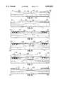
- FIG. 1is a schematic cross-sectional view of a semiconductor device with a capacitor formed thereon;
- FIG. 2is a plan view of a portion of a wafer having capacitors formed thereon;
- FIGS. 3 to 7illustrate the various processing steps involved in fabricating capacitors in accordance with the invention.
- FIG. 8shows an alternative embodiment
- a silicon substrate 1has various components, such as transistors and the like (not shown) formed therein by previous process steps known in the art.
- a layer of polysilicon 2is first deposited on the surface of the wafer and patterned to provide a contact for the bottom electrode for the capacitor 10.
- the insulating layer 3typically consists of a lower layer of silicate glass, an intermediate layer of phosphorus-doped silicate glass (containing 4 wt. % P), and an upper layer of inorganic spin-on glass (also containing 4 wt. % P).
- the formation of such an insulating layeris conventional and well understood to a person skilled in the art.
- Layer 3typically has a total nominal thickness of 0.8 micron.
- a first extra mask(not shown) a series of arrays of holes 5 are etched in the insulating layer 3. Each array will form a capacitor in a manner to be described.
- This maskis referred to as an extra mask because it involves a masking step over and above what would normally be required in conventional integrated circuit processing.
- a lower electrode 7is sputtered onto the insulating layer 3 in a sputtering chamber initially in the presence of an inert gas, such as argon.
- the lower electrode layer 7consists of a titanium layer followed by a titanium nitride layer.
- the lower Ti sublayeris preferred in order to make a good electrical contact with the underlying polysilicon layer 2.
- the titanium nitride layercan be deposited by changing the inert gas in the sputtering chamber to nitrogen. This electrode layer 7 typically has a total thickness of 0.01 to 0.1 microns.
- a titanium oxide (TiO 2 ) layer 8is formed, typically by thermal oxidation at 400-500° C. for less than about thirty seconds (or by plasma oxidation at about 200° C. for about 2 mins) on the titanium nitride sublayer.
- the oxide layercan be formed by rapid thermal oxidation (RTO) at 700° C. for about 1 minute. This oxide layer typically has a thickness of 50 to 1000 Angstroms.
- the free titaniumcan be oxidized in situ in the metallization tool.
- the waferis transferred to a second chamber where it is placed in 1% of oxygen in argon plasma for about one minute. This creates a seed oxidation layer from the free titanium, which enhances subsequent oxidation.
- the waferis returned to the sputtering chamber, and the upper electrode layer 9, consisting of a TiN or preferably a TiN Ti/TiN sandwich is deposited.
- This upper layer 9has a thickness of about 0.01 to 0.1 microns.
- dielectric layer 8is deposited in a separate system, other suitable dielectrics can be employed, for example, silicon nitride (Si 3 N 4 ), although this does not have as good dielectric properties as TiO 2 .
- silicon nitrideSi 3 N 4
- Another possibilityis to employ a combination of TiO 2 and (Si 3 N 4 ).
- FIG. 3shows the wafer prior to the formation of the capacitors 10.
- the devicehas a field oxide layer 20 in the silicon substrate 1 and a transistor 25 having source 21, drain 22, gate oxide 23, and gate 24.
- the gate 24is a polysilicon layer that is deposited with the contacts 2 as a common layer which is then patterned to make the bottom electrode contacts 2 and the gate electrodes 24.
- the SG/PSG/SOG layer 3is then deposited as shown in FIG. 4 and the capacitors 10 formed as described with reference to FIG. 1.
- the capacitor layers 7, 8, 9of course extend across the whole wafer.
- the next stepis to pattern the individual capacitors. As this step requires an additional mask over and above that normally used, this is considered a second extra masking step. A conventional mask can be employed.
- an isolation oxide layer 30is applied across the whole wafer to give a structure as shown in FIG. 4.
- the isolation oxide layeris applied by PECVD to isolate the individual capacitors 10. This isolation layer is necessary to ensure that the edge 10' of the layers 7, 8, 9, of the capacitors 10 are protected against shorts when subsequent metal interconnect layers 41 are applied.
- the next stepis to mask the isolation layer 30 and etch holes 40 through the dielectric 3 to reach to the source, drain and gate regions of the transistors 1.
- This stepis conventional.
- metal interconnect layer 41typically an aluminum alloy with a TiN anti-reflective coating
- the interconnect layer 41extends into the holes 40 to establish contact with the source 21, drain 22, and gate 24 of the transistors 25.
- This layerconsists of a conventional ID 1 /SOG/ID 2 layer, where ID stands for interlayer dielectric. ID is typically SRSG (silicon rich silicon glass) and the SOG in this case is typically a semi-organic spin-on glass.
- IDstands for interlayer dielectric.
- IDis typically SRSG (silicon rich silicon glass) and the SOG in this case is typically a semi-organic spin-on glass.
- a mask(not shown) is applied and via holes 51 are etched through the layer 50 to the upper electrode 9 of isolating the capacitors 10 and to the layer 41 where it is desired to establish interconnections. This is a standard procedure.
- a second aluminum interconnect layer 52(M 2 layer) is applied over the layer 51.
- the M 2 layeris used in conventional i.c. processing to establish connections to the M 1 layer, and in this case is used additional to establish connection with the upper electrodes 9 of the capacitors.
- the layer 52is subsequently patterned in a conventional manner.
- the M 1 layer 41is generally much thicker than the upper electrode layer 9, there is no risk of over-etching because the via holes 51 reach the interconnect layer 41 before they reach the thinner electrode layer 9. Etching can be terminated as soon as the holes reach electrode layer 9. There is thus no risk of an over-etch causing destruction of the capacitors, yet contact with both the electrode layer 9 and the interconnect layer 41 is assured.
- FIG. 8shows an alternative embodiment, where conventional capacitors 60 are formed prior to making the conformal capacitors 10 and then connected in parallel.
- capacitors 60are formed by first providing an additional poly layer 61 under the poly layer 2.
- a dielectric layer 62is formed between the two poly layers 2, 61.
- additional capacitors 10can be formed on top of the conventional capacitors in a manner described above.
- the capacitors 10 and 60are connected in parallel to create a composite capacitor having a capacitance equal to the sum of the two individual capacitances.
- FIG. 2is a plan view of a portion of a wafer showing the capacitors 10 consisting of arrays of holes 5. Connection to the lower poly layers 2 is by means of connections 2'.
- the holestypically have a diameter and spacing of about 1 micron.
- the described methodpermits high value capacitors to be formed in an economic manner with only two additional masking steps.
- the only extra masking steps requiredare the first extra mask to form the holes 5 and the second extra mask to pattern the capacitors.
- Extra deposition stepsare required to form the capacitors, but the remaining connections are made using standard processing steps.
- the methodis particularly suitable for working a 0.8 micron line widths and below. Also, the capacitors have metal electrodes, which lead to extremely good voltage coefficients.
Landscapes
- Semiconductor Integrated Circuits (AREA)
- Semiconductor Memories (AREA)
Abstract
Description
Claims (15)
Applications Claiming Priority (2)
| Application Number | Priority Date | Filing Date | Title |
|---|---|---|---|
| GB9810797AGB2337633B (en) | 1998-05-20 | 1998-05-20 | Method of forming capacitors in a semiconductor device |
| GB9810797 | 1998-05-20 |
Publications (1)
| Publication Number | Publication Date |
|---|---|
| US6083805Atrue US6083805A (en) | 2000-07-04 |
Family
ID=10832362
Family Applications (1)
| Application Number | Title | Priority Date | Filing Date |
|---|---|---|---|
| US09/314,105Expired - LifetimeUS6083805A (en) | 1998-05-20 | 1999-05-19 | Method of forming capacitors in a semiconductor device |
Country Status (4)
| Country | Link |
|---|---|
| US (1) | US6083805A (en) |
| JP (1) | JPH11354720A (en) |
| CA (1) | CA2272170A1 (en) |
| GB (1) | GB2337633B (en) |
Cited By (9)
| Publication number | Priority date | Publication date | Assignee | Title |
|---|---|---|---|---|
| US6284586B1 (en)* | 1996-06-28 | 2001-09-04 | Lsi Logic Corporation | Integrated circuit device and method of making the same using chemical mechanical polishing to remove material in two layers following masking |
| US20030060003A1 (en)* | 2001-08-31 | 2003-03-27 | Thomas Hecht | Capacitor device for a semiconductor circuit configuration, and fabrication method |
| US6551890B2 (en)* | 1999-03-10 | 2003-04-22 | Koninklijke Philips Electronics N.V. | Method of manufacturing a semiconductor device comprising a bipolar transistor and a capacitor |
| US6576526B2 (en) | 2001-07-09 | 2003-06-10 | Chartered Semiconductor Manufacturing Ltd. | Darc layer for MIM process integration |
| US20040147085A1 (en)* | 2002-12-24 | 2004-07-29 | Bo-Yeoun Jo | Method for fabricating a capacitor using a metal insulator metal structure |
| US20050277304A1 (en)* | 2004-06-10 | 2005-12-15 | Dalsa Semiconductor Inc. | Titanium silicate films with high dielectric constant |
| CN102339869A (en)* | 2010-07-16 | 2012-02-01 | 美格纳半导体有限公司 | Semiconductor device with MIM capacitor and manufacturing method thereof |
| US8940388B2 (en) | 2011-03-02 | 2015-01-27 | Micron Technology, Inc. | Insulative elements |
| US20160315255A1 (en)* | 2015-04-27 | 2016-10-27 | Winbond Electronics Corp. | Resistive random access memory |
Families Citing this family (2)
| Publication number | Priority date | Publication date | Assignee | Title |
|---|---|---|---|---|
| JP2002184946A (en) | 2000-12-11 | 2002-06-28 | Murata Mfg Co Ltd | MIM capacitor and method of manufacturing the same |
| GB2434312B (en) | 2006-01-18 | 2011-06-29 | Gw Pharma Ltd | Cannabinoid-containing plant extracts as neuroprotective agents |
Citations (3)
| Publication number | Priority date | Publication date | Assignee | Title |
|---|---|---|---|---|
| US5576240A (en)* | 1994-12-09 | 1996-11-19 | Lucent Technologies Inc. | Method for making a metal to metal capacitor |
| US5858832A (en)* | 1996-03-11 | 1999-01-12 | Chartered Semiconduction Manufacturing Ltd. | Method for forming a high areal capacitance planar capacitor |
| US5985731A (en)* | 1998-08-17 | 1999-11-16 | Motorola, Inc. | Method for forming a semiconductor device having a capacitor structure |
Family Cites Families (3)
| Publication number | Priority date | Publication date | Assignee | Title |
|---|---|---|---|---|
| JP2723530B2 (en)* | 1988-04-13 | 1998-03-09 | 日本電気株式会社 | Method for manufacturing dynamic random access memory device |
| JP2818964B2 (en)* | 1990-03-30 | 1998-10-30 | 三菱電機株式会社 | Manufacturing method of semiconductor memory device having charge storage portion of laminated structure |
| JP2897631B2 (en)* | 1993-12-28 | 1999-05-31 | 日本電気株式会社 | Semiconductor integrated circuit device and manufacturing method |
- 1998
- 1998-05-20GBGB9810797Apatent/GB2337633B/ennot_activeExpired - Fee Related
- 1999
- 1999-05-18CACA002272170Apatent/CA2272170A1/ennot_activeAbandoned
- 1999-05-19JPJP11138247Apatent/JPH11354720A/enactivePending
- 1999-05-19USUS09/314,105patent/US6083805A/ennot_activeExpired - Lifetime
Patent Citations (3)
| Publication number | Priority date | Publication date | Assignee | Title |
|---|---|---|---|---|
| US5576240A (en)* | 1994-12-09 | 1996-11-19 | Lucent Technologies Inc. | Method for making a metal to metal capacitor |
| US5858832A (en)* | 1996-03-11 | 1999-01-12 | Chartered Semiconduction Manufacturing Ltd. | Method for forming a high areal capacitance planar capacitor |
| US5985731A (en)* | 1998-08-17 | 1999-11-16 | Motorola, Inc. | Method for forming a semiconductor device having a capacitor structure |
Cited By (12)
| Publication number | Priority date | Publication date | Assignee | Title |
|---|---|---|---|---|
| US6284586B1 (en)* | 1996-06-28 | 2001-09-04 | Lsi Logic Corporation | Integrated circuit device and method of making the same using chemical mechanical polishing to remove material in two layers following masking |
| US6551890B2 (en)* | 1999-03-10 | 2003-04-22 | Koninklijke Philips Electronics N.V. | Method of manufacturing a semiconductor device comprising a bipolar transistor and a capacitor |
| US6576526B2 (en) | 2001-07-09 | 2003-06-10 | Chartered Semiconductor Manufacturing Ltd. | Darc layer for MIM process integration |
| US20030060003A1 (en)* | 2001-08-31 | 2003-03-27 | Thomas Hecht | Capacitor device for a semiconductor circuit configuration, and fabrication method |
| US20040147085A1 (en)* | 2002-12-24 | 2004-07-29 | Bo-Yeoun Jo | Method for fabricating a capacitor using a metal insulator metal structure |
| US7247572B2 (en)* | 2002-12-24 | 2007-07-24 | Dongbu Electronics Co., Ltd. | Method for fabricating a capacitor using a metal insulator metal structure |
| US20050277304A1 (en)* | 2004-06-10 | 2005-12-15 | Dalsa Semiconductor Inc. | Titanium silicate films with high dielectric constant |
| US7101754B2 (en) | 2004-06-10 | 2006-09-05 | Dalsa Semiconductor Inc. | Titanium silicate films with high dielectric constant |
| CN102339869A (en)* | 2010-07-16 | 2012-02-01 | 美格纳半导体有限公司 | Semiconductor device with MIM capacitor and manufacturing method thereof |
| CN102339869B (en)* | 2010-07-16 | 2016-01-06 | 美格纳半导体有限公司 | There is semiconductor device and the manufacture method thereof of MIM capacitor |
| US8940388B2 (en) | 2011-03-02 | 2015-01-27 | Micron Technology, Inc. | Insulative elements |
| US20160315255A1 (en)* | 2015-04-27 | 2016-10-27 | Winbond Electronics Corp. | Resistive random access memory |
Also Published As
| Publication number | Publication date |
|---|---|
| JPH11354720A (en) | 1999-12-24 |
| GB9810797D0 (en) | 1998-07-15 |
| CA2272170A1 (en) | 1999-11-20 |
| GB2337633A (en) | 1999-11-24 |
| GB2337633B (en) | 2003-04-02 |
Similar Documents
| Publication | Publication Date | Title |
|---|---|---|
| US4455568A (en) | Insulation process for integrated circuits | |
| KR100252447B1 (en) | Raised tungsten plug antifuse and fabrication process | |
| US5918135A (en) | Methods for forming integrated circuit capacitors including dual electrode depositions | |
| JP2007221161A (en) | Capacitor used in semiconductor device and manufacturing method thereof | |
| JPH06224304A (en) | Anti-fuse element and preparation | |
| KR100306202B1 (en) | Semiconductor device and manufacturing method thereof | |
| US6083805A (en) | Method of forming capacitors in a semiconductor device | |
| KR20000057879A (en) | Semiconductor device having interconnection implemented by refractory metal nitride layer and refractory metal silicide layer and process of fabrication thereof | |
| US6246120B1 (en) | Sidewalls for guiding the via etch | |
| KR100430924B1 (en) | Integrated circuit and method for producing the same | |
| KR100480469B1 (en) | Method for manufacturing capacitor in a semiconductor device | |
| KR100212689B1 (en) | How to Form Contact Plugs | |
| US5913126A (en) | Methods of forming capacitors including expanded contact holes | |
| US6893935B2 (en) | Semiconductor component and fabrication method | |
| JPH11506869A (en) | Double half via antifuse | |
| US5420077A (en) | Method for forming a wiring layer | |
| KR100270962B1 (en) | Method for fabricating capacitor of semiconductor integrated circuit | |
| US6146987A (en) | Method for forming a contact plug over an underlying metal line using an etching stop layer | |
| US5834367A (en) | Method of manufacturing semiconductor device having a multilayer wiring | |
| KR100997776B1 (en) | Method of manufacturing semiconductor device | |
| JPH104092A (en) | Method of fabricating semiconductor device | |
| KR960011816B1 (en) | Method of making a capacitor in semiconductor device | |
| CN1139820A (en) | Semiconductor element interconnection device and manufacturing method thereof | |
| JP2555755B2 (en) | Semiconductor device and manufacturing method thereof | |
| KR100609537B1 (en) | Manufacturing Method of Semiconductor Device |
Legal Events
| Date | Code | Title | Description |
|---|---|---|---|
| AS | Assignment | Owner name:MITEL CORPORATION, CANADA Free format text:ASSIGNMENT OF ASSIGNORS INTEREST;ASSIGNORS:OUELLET, LUC;BLAIN, STEPHANE;REEL/FRAME:010083/0227;SIGNING DATES FROM 19990513 TO 19990514 | |
| AS | Assignment | Owner name:CANADIAN IMPERIAL BANK OF COMMERCE, AS SECURED PAR Free format text:GRANT OF PATENT SECURITY INTEREST;ASSIGNOR:MITEL CORPORAITON A CORPORATION OF CANADA;REEL/FRAME:010231/0330 Effective date:19990630 | |
| STCF | Information on status: patent grant | Free format text:PATENTED CASE | |
| AS | Assignment | Owner name:MITEL CORPORATION, CANADA Free format text:RELEASE BY SECURED PARTY;ASSIGNOR:CANADIAN IMPERIAL BANK OF COMMERCE;REEL/FRAME:011590/0406 Effective date:20010216 Owner name:MITEL, INC., A DELAWARE CORPORATION, CANADA Free format text:RELEASE BY SECURED PARTY;ASSIGNOR:CANADIAN IMPERIAL BANK OF COMMERCE;REEL/FRAME:011590/0406 Effective date:20010216 Owner name:MITEL SEMICONDUCTOR, INC., A DELAWARE CORPORATION, Free format text:RELEASE BY SECURED PARTY;ASSIGNOR:CANADIAN IMPERIAL BANK OF COMMERCE;REEL/FRAME:011590/0406 Effective date:20010216 Owner name:MITEL SEMICONDUCTOR, LIMITED, CANADA Free format text:RELEASE BY SECURED PARTY;ASSIGNOR:CANADIAN IMPERIAL BANK OF COMMERCE;REEL/FRAME:011590/0406 Effective date:20010216 Owner name:MITEL TELCOM LIMITED CORPORATION, CANADA Free format text:RELEASE BY SECURED PARTY;ASSIGNOR:CANADIAN IMPERIAL BANK OF COMMERCE;REEL/FRAME:011590/0406 Effective date:20010216 Owner name:MITEL SEMICONDUCTOR AMERICAS, INC., A DELAWARE COR Free format text:RELEASE BY SECURED PARTY;ASSIGNOR:CANADIAN IMPERIAL BANK OF COMMERCE;REEL/FRAME:011590/0406 Effective date:20010216 | |
| AS | Assignment | Owner name:ZARLINK SEMICONDUCTOR INC., ONTARIO Free format text:CHANGE OF NAME;ASSIGNOR:MITEL CORPORATION;REEL/FRAME:012653/0397 Effective date:20010725 | |
| AS | Assignment | Owner name:DALSA SEMICONDUCTOR INC., CANADA Free format text:ASSIGNMENT OF ASSIGNORS INTEREST;ASSIGNOR:ZARLINK SEMICONDUCTOR INC.;REEL/FRAME:013305/0508 Effective date:20020222 | |
| FPAY | Fee payment | Year of fee payment:4 | |
| FPAY | Fee payment | Year of fee payment:8 | |
| AS | Assignment | Owner name:TELEDYNE DALSA SEMICONDUCTOR INC., CANADA Free format text:CHANGE OF NAME;ASSIGNOR:DALSA SEMICONDUCTOR INC.;REEL/FRAME:027064/0622 Effective date:20110214 | |
| FPAY | Fee payment | Year of fee payment:12 |