US6083047A - Modular electrical PCB assembly connector - Google Patents
Modular electrical PCB assembly connectorDownload PDFInfo
- Publication number
- US6083047A US6083047AUS08/784,743US78474397AUS6083047AUS 6083047 AUS6083047 AUS 6083047AUS 78474397 AUS78474397 AUS 78474397AUS 6083047 AUS6083047 AUS 6083047A
- Authority
- US
- United States
- Prior art keywords
- module
- circuit
- electrical connector
- region
- connector
- Prior art date
- Legal status (The legal status is an assumption and is not a legal conclusion. Google has not performed a legal analysis and makes no representation as to the accuracy of the status listed.)
- Expired - Lifetime
Links
Images


Classifications
- H—ELECTRICITY
- H01—ELECTRIC ELEMENTS
- H01R—ELECTRICALLY-CONDUCTIVE CONNECTIONS; STRUCTURAL ASSOCIATIONS OF A PLURALITY OF MUTUALLY-INSULATED ELECTRICAL CONNECTING ELEMENTS; COUPLING DEVICES; CURRENT COLLECTORS
- H01R13/00—Details of coupling devices of the kinds covered by groups H01R12/70 or H01R24/00 - H01R33/00
- H01R13/648—Protective earth or shield arrangements on coupling devices, e.g. anti-static shielding
- H01R13/658—High frequency shielding arrangements, e.g. against EMI [Electro-Magnetic Interference] or EMP [Electro-Magnetic Pulse]
- H01R13/6581—Shield structure
- H01R13/6585—Shielding material individually surrounding or interposed between mutually spaced contacts
- H01R13/6586—Shielding material individually surrounding or interposed between mutually spaced contacts for separating multiple connector modules
- H01R13/6587—Shielding material individually surrounding or interposed between mutually spaced contacts for separating multiple connector modules for mounting on PCBs
Definitions
- the present inventionrelates to connectors and specifically to high speed, shielded connectors having one or more integrated PCB assemblies.
- Connectorshaving insulative bodies and individual metal terminals are now widely used and available in many different configurations.
- the usual method of manufacturecomprises stitching or insert molding terminals into a suitable housing.
- the manufacturing processmay also include a terminal tail bending operation, especially for right angle connectors.
- Connectors for high-frequency applicationspresent additional requirements.
- controlled-impedance terminal sections with ground shielding optionsare preferred.
- U.S. Pat. No. 4,571,014shows a different approach for making backplane connectors using one or more PCB assemblies.
- Each of the PCB assembliescomprises one insulated substrate, one spacer, and one cover plate, all of which are attached to one another.
- the insulating substrateis provided with a predetermined pattern of conducting tracks, while ground tracks are provided between the conducting tracks.
- the conducting tracksare connected at one end to a female contact terminal and at the other end to a male contact terminal.
- Each of the cover platesis a conductive shield member.
- the circuit substratesare arranged with the sides bearing the conductive tracks all facing in the same direction.
- the cover plates/shieldsare each interleaved between adjacent substrates. While such an arrangement produces a plurality of individual shielded tracks, it does not present the possibility for creating impedance matched pairs of conductive tracks through the connector, in a twinax configuration.
- Twinax connectorsare often utilized in combination with twisted pair cable. Such twisted pair cables usually have a plurality of pairs of identical conductors twisted along the signal transmission length.
- Such a conductor pairhas the signal over the two conductors as differential pair; this conductor pair (and possibly several twisted pairs) is enclosed within an outer copper shielding braid to form a cable. Often each twisted pair may have an individual drain wire. Because the electromagnetic flux generated on the twisted pair of a conductor are equal in magnitude and opposite in direction, effectively they cancel each other. Extending this concept to a pair of twinax connector contacts, this can be envisaged as two adjacent, spaced contact elements contained within an outer (rectangular cross-section) grounding shell. This is a relatively inexpensive method to maintain signal quality through an interconnection. Often this is referred to a "balanced pair" interconnection.
- twinax interconnection terminationis often related to the use of cable, but similarly a twinax connector may be terminated on a PCB.
- the connectorinstead of the cable twisting, the connector can be mounted on a PCB having pairs of identical tracks which are located spatially adjacent to each other, usually as part of a multi-layered structure.
- U.S. Pat. No. 4,571,014discloses primarily a backplane interconnection and not a cable-to-cable or cable-to-board interconnection.
- PCT Patent Application Ser. No. US96/11214 filed Jul. 2, 1996discloses board to board connectors made from stacked modules, each module being formed of a printed circuit board assembly and a cover. This application discloses high speed board to board connectors that have relatively low manufacturing costs.
- the object of the present inventionis to provide a connector which overcomes the disadvantages described above.
- This objectis obtained by the present invention by providing a connector in which connector terminals are associated with conductive tracks or traces on a PCB adapted to function as conductive leads of the connector.
- PCB'sare arranged to provide pairs of electrically matched conductive traces, by placing traces in a substantially mirror-image relationship.
- ground tracksmay be provided between the conducting tracks on a first surface and a ground layer may be provided on a second surface opposite the first surface.
- the coversare made of insulating material and may hold one or more insulating substrates with conductive traces in opposed relationship to form matched pairs of conductive traces.
- the covers, together with one or more associated PCB's,may form modules that are assembled in side-by-side relationship in a housing to form a completed connector.
- the connectormay also comprise an insulating connector body accommodating each of said one or more integrated PCB assemblies and provided with a metallized shielding layer on its outer surface. Thereby, the electromagnetic interference caused by such a connector to the environment is further reduced.
- the connector bodydesirably includes structure for receiving and securing PCB modules in alignment.
- the PCB modulesinclude structure for retaining flexible conductors, such as wires or cables, in a position to be secured to traces on the PCB.
- the coverscan include such retaining structures.
- FIGS. 1a-1cshow construction techniques broadly applicable to connectors embodying the invention
- FIG. 2is a side elevational view of a PCB assembly according to one embodiment of the invention.
- FIGS. 3, 4 and 5are fragmentary views showing the mounting of terminals on the PCB assembly shown in FIG. 2;
- FIGS. 6-6dshow different views of an insulative cover to be used in conjunction with the PCB assembly of FIG. 2 to form a terminal column module;
- FIGS. 7-7eillustrate an assembled terminal module formed of a PCB assembly as shown in FIG. 2 and a cover as shown in FIG. 6;
- FIGS. 8-8a and 9are enlarged views showing portions of the integrated terminal column module shown in FIG. 7;
- FIGS. 10-10cshown views of a connector housing for receiving a plurality of modules as illustrated in FIG. 7;
- FIGS. 11-11a and 11bshow various views of a lead-in plate for the housing shown in FIG. 10.
- FIG. 12illustrates two PCB assemblies having a mirror-image relationship
- FIG. 13is a generalized cross-section of two PCB assemblies positioned in back-to-back relationship to form matched pair or twinax conductor paths;
- FIG. 14shows a shielded pair module with spaced PCB assemblies
- FIG. 15is a rear view of an assembled connector having a plurality of shielded pair PCB assemblies
- FIG. 16is a rear view of an assembled connector having individually shielded signal traces
- FIGS. 17a, 17b and 17cshow several PCB arrangements for forming shielded connectors
- FIGS. 18a and 18bare schematic circuit diagrams of the arrangements shown in FIGS. 17a-17b and FIG. 17c, respectively;
- FIGS. 19, 19a and 19bshow a cover for use with cable connectors
- FIG. 20ais an exploded isometric view of a twinax cable connector module
- FIG. 20bis an isometric view of the module of FIG. 20a in assembled form and positioned for insertion into a connector housing;
- FIG. 20cis an isometric view of a completed right angle cable connector
- FIG. 21ais an exploded isometric view of a twinax straight cable connector module
- FIG. 21bis an isometric view of the module of FIG. 21a in assembled form and positioned for insertion into a connector housing;
- FIG. 21cis an isometric view of a completed straight cable connector.
- FIGS. 1a-1cgenerally show manufacturing steps for producing a right angle connector according to the invention in which standard methods of producing printed circuit boards are used.
- FIG. 1ashows an insulating substrate 16, formed for example of conventional flat PCB material provided with several parallel conducting signal tracks 11.
- Conducting ground tracks 10may be provided between adjacent tracks 11.
- the outer most conducting ground track 10is provided with a ground contact terminal 7 to be connected to ground through the printed circuit board on which the connector is to be mounted.
- Each of the conducting tracks 11is connected to board contact terminals 7, the board contact portions 15 of which extending beyond the circuit substrate 16.
- the board contact portions 15are shown as press-fit terminals they might be replaced by suitable solder tail terminals.
- the other ends of the conducting tracks 11are connected to suitable contact terminals 4.
- the terminals 4 and 7, respectivelyare fixed onto suitable solder pads formed at the ends of traces 11. This can be achieved by conventional surface mount soldering techniques.
- An insulating spacer 17can be provided having a first series of openings 24 for accommodating the contact terminals 4 and a second series of openings 25 for accommodating at least part of the board contact terminals 7.
- the recess 2 in the module 1is formed at the interface of adjacent layers or laminations. That is, the recesses 2, for example, are bounded by the circuit substrate 16, the edges of openings 24 or 25 and the cover 18. This allows the contacts to be secured on substrate 16 by conventional surface mounting or other bonding techniques.
- the cover 18 and spacer 17are combined into a single molded part.
- FIG. 1bshows one integrated PCB assembly manufactured from the components shown in FIG. 1a, i.e. an insulating substrate 16 to which an insulating spacer 17 is attached and an insulating cover plate 18 attached to the insulating spacer 17.
- the first series of openings 24 in the insulating spacer 17form recesses 2, in which the receptacle terminals 4 are disposed to receive contact terminals of a mating connector (not shown).
- the receptacle terminals 4 shown in FIG. 1amay be replaced by pins or hermaphrodite contact terminals.
- a cover platecould be provided in which suitable recesses are made for accommodating the contact terminals 4 and the board contact terminals 7.
- Such recesseswould serve the same purpose as openings 24, 25 in spacer 17 shown in FIG. 1a.
- such recessescould be provided in substrate 16.
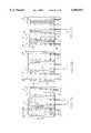
- FIG. 1cshows several integrated PCB modules as shown in FIG. 1b arranged parallel, side-by-side relationship for insertion into a connector body 19.
- the connector body 19may be made of any insulating material and may be provided with a metallized inner surface to enhance the shielding effectiveness.
- the connector body 19may be provided with suitable guiding ridges 23 and one or more guiding extensions 22 for properly connecting the assembled connector to a mating connector (not shown).
- one or more locating and securing posts 21, receivable within a hole in a printed circuit board to which the connectors to be connected,is provided at the bottom side of the connector body 19.
- the connector body 19is provided with suitable lead-in holes 20 in corresponding relationship with each of the contact terminals 4.
- Each of the lead-in holes 20is suitable for receiving a mating pin terminal of a mating connector (not shown).
- the lead-in holes 20are arranged in columns and rows as is designated by arrows c and r.
- the PCB assembly 30comprises an insulating substrate 31 of a material commonly commercially used for making PCBs.
- the substrate 31can be a resin impregnated fiber material, such as is sold under the designation FR4, having a thickness 0.4 mm, for example.
- FR4resin impregnated fiber material
- the traces 32include contact pads at each end adapted to have metal terminals secured to them, as by conventional surface mounting techniques using solder.
- a plurality of ground or shielding traces 33are also be applied to the substrate 31.
- the shielding traces 33are preferably disposed between each of the circuit traces 32.
- a terminal, such as a contact terminal 34is mounted at the first end of each trace 32 and a connector mounting side terminal 35 is mounted on the second end of each circuit trace 32.
- An additional shielding or ground layer 36may be applied to the remainder of the substrate 31.
- a ground terminal 37is fixed onto the ground layer 36, in alignment with the terminals 35.
- a locating hole 39may be appropriately placed in the substrate 31.
- the locating hole 39preferably comprises a plated through hole for establishing electrical connection with a grounding layer 38 (FIG. 5) that may extend substantially over the entire back surface of the substrate 31.
- Small vias forming plated through-holesmay be disposed in each of the ground tracks 33 so that the ground tracks 33, the shield layer 36 and the back shield layer 38 form a shielding structure for the signal traces 32 and associated terminals. If no shielding or limited shielding is desired, one or more of the shielding structures 33, 36 or 38 can be eliminated.
- contact terminals 34are formed as a one-piece stamping and can comprise a dual beam contact having a base section 40 having an opposed pair of upstanding portions 41.
- a spring section 42is cantilevered from each of the upstanding portions 41 to define an insertion axis for a mating terminal, such as a pin from a pin header. Such a mating pin would engage the contact portions 43 disposed at the end of each cantilevered arm 42.
- the contact terminalsalso include a mounting section, such as the planar member 44, that is adapted to be secured onto the end of the circuit trace 32, typically by solder 46. The latter can be accomplished by conventional surface mounting or other bonding techniques.
- the cantilevered arms 42 and contact portions 43define a contact mating or pin insertion axis that is generally parallel to the plane of substrate 31, but is offset from the surface carrying the conductive traces 32.
- one preferred form of connector mounting terminal 35includes a press-fit section 48 and a board mounting section 49.
- the board mounting section 49includes a generally planar base 50 with an upturned top tang 52 disposed along a top edge. A pair of opposed side tangs 53 are also upturned from the base 50.
- the mounting portion 49is retained on the circuit trace 32 by solder fillets 54, again formed by conventional surface mounting solder techniques.
- the top tang 52is spaced closely adjacent to or rests on the top surfaces of the side tangs 53 as shown in FIG. 5.
- FIGS. 6, 6a, 6b, 6c and 6dillustrate an insulative cover/spacer member 56, preferably molded from an appropriate polymeric insulating material.
- the coverincludes a plurality of contact recesses 57 formed along one edge. Each of the recesses 57 includes a contact preload rib 58. A large central recess 59 may also be formed in the cover. A second plurality of terminal recesses 60 is formed along a second edge of the cover. Further, a locating boss 62 is integrally formed with the cover and is sized and shaped to be received, with limited clearance, in the locating opening 39 in the substrate 31.
- the coverfurther includes an upper rim 63 extending from the rear of the cover to a location near the recesses 57.
- a bottom rim or support member 64is formed on a portion of the bottom surface of the cover.
- the cover 56further includes an upper locating and mounting rib 65, preferably in the form of a dove tail rib as shown.
- a similar but shorter mounting and locating rib 66is disposed on the bottom edge of the cover.
- the surfaces 67a and 67bform board rest surfaces against which a substrate 31 is placed.
- the surfaces 67a and 67bmay carry an adhesive or alternately a double sided adhesive coated film (not shown) may be applied to extend from surface 67a to surface 67b.
- FIG. 7is substantially an x-ray view through the cover 56 of column terminal module 69.
- the PCB assembly 30is located in the vertical direction by the upper and lower rim or mounting members 63, 64 and is located in a longitudinal manner by the locating boss 62 (see also FIG. 7e).
- the contact terminals 34are located in the contact recesses 57 and the connector mounting terminals 35 are located in the recesses 60.
- the previously mentioned adhesive or adhesive coated films on surface 67a and 67bmaintain the PCB assembly and cover 56 together.
- FIG. 7ais a sectional view taken along line AA of FIG. 7 and shows the contact terminals 34 located in the contact recesses 57.
- the terminals 34are positioned so that the contact portions 43 bear against the preload ribs 58 to impart a desired preload on the cantilevered spring arms 42.
- FIG. 7bis a sectional view taken along line BB of FIG. 7. As shown in FIG. 7b, the substrate 31 is essentially located in a vertical position by the rims 63 and 64.
- each connector mounting terminal 35has its mounting portion received within a corresponding recess 60.
- the board mounting terminalis of a type that is likely to have a relatively high axial force applied to it, such as a press-fit terminal, the surface 68 (FIG. 6d) of the recess 60 is advantageously located so that it bears against the upturned tang 52 of the terminal.
- FIG. 7c and FIG. 9are taken substantially along section line cc of FIG. 7.
- FIG. 7dis a fragmentary cross sectional view taken along line DD of FIG. 7, showing the positioning of grounding terminal 37 in a similar fashion to terminals 35 shown in FIG. 7c and FIG. 9 (discussed below).
- FIG. 7eis a view of the back end of the module 69 showing in phantom views the locating boss 62 and the mounting portion of terminal 37.
- FIGS. 8 and 8aillustrate enlarged views of the connector contacts 34 located in recesses 57 of the cover 56.
- FIG. 8ais a cross sectional view taken along line GG of FIG. 8 and shows the positioning of the pre-load rib 58 with respect to the contact portions 43.
- FIG. 9illustrates the interaction of the cover 56 with the board connection terminal 35 when a downward force F is applied to the top edge of the module 69. That force is transmitted by the cover to the pressing surface 68 formed by the top surface of the recess 60. As a result, a vertical insertion force that is used to push the press-fit 48 section into the hole T is applied directly to the upper tang 52 and the side tangs 53. In this manner, shear stress occurring at the solder connection between the base 50 of the terminal and the circuit trace 32 is minimized. In this manner, loosening or detachment of the terminal 35 is avoided.
- the surface 68is designed so that it will engage tang 52 before the rim 63 begins applying a vertical force to the upper edge of the substrate 31.
- One way to accomplish thisis to provide an initial, small clearance between the rim 63 and the adjacent edge of substrate 31.
- the coveris designed so that a significant proportion of the insertion force is applied directly to terminal 35 so that stress at the terminal/conductive track interface is minimized.
- the structure disclosedis designed to withstand required press-fit pin insertion forces of 35-50 Newtons per pin.
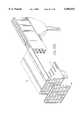
- FIG. 10is a cross sectional view taken along line HH of FIG. 10a and shows a connector housing 70 having a top wall 72, a bottom wall 76 and a front wall 78.
- the top wall 72includes a plurality of locating slots, for example the dove tail slots 73.
- One or more guiding ridges 74may be formed on a top surface of the top 72.
- the bottom 76also includes locating slots, for example the dove tail slots 77.
- the front wall 78includes a plurality of openings 79. Additional shielding can be provided by metallizing appropriate surfaces of the housing 70.
- FIG. 10cshows a bottom view of the housing 70 shown in FIG. 10.
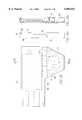
- FIG. 11is a front elevational view of a lead-in face plate 80 having a plurality of tapered lead-in sections 84 arranged in the form of a grid. Each of the lead-in portions 84 extends to a pin insertion port 85. A plurality of sleeves or hollow bosses 86 extend from the rear surface of the face plate 80 and are shaped and sized to be positioned and retained in the openings 79 in the front wall 78 of housing 70. The use of a separate lead-in plate is desirable when the interior surfaces of the housing 70 are to be fully metallized. However, the housing 70 can also be formed with the lead-in plate integrally molded, where selective metallization or no metallization is utilized.
- FIG. 12illustrates printed circuit board modules configured to provide connectors having shield pairs of terminals.
- the module 30 shown in the lower portion of FIG. 12is essentially the same as the module illustrated in FIG. 7 wherein the dotted lines illustrate the location of structures on the side of cover 56 located on the reverse side of the cover adjacent PCB 31 (FIG. 7C). For purposes of clarity, traces 32 and 33 have been shown in full line rather than dotted or phantom form.
- the elements forming the module 30are the same as those discussed in connection with FIGS. 2-9 and no further description thereof is believed necessary.
- PCB module 30'includes essentially the same elements as module 30 and these have been designated by the designation. Module 30' differs from module 30 essentially in the aspect that the elements of this module are arranged to constitute a mirror-image with a respect to line L.
- FIG. 13illustrates a generalized cross-sectional view of modules 30 and 30' arranged in back to back relationship to form a complete shielded pair module that can be placed in side by side relationship with similar modules to form a connector.
- the back shielding layers 38, 38' of the PCB's 31, 31'are arranged adjacent one another to form the shielded pair module.
- the modules 30, 30'can be held in the illustrated relationship by insertion into housing 70 (FIG. 10) or, if desired, by a conductive adhesive layer applied to adjacent outer surfaces of shielding layers 38, 38'.
- the dimension Xrepresents the centerline distance between the terminals 34 and 34', which essentially constitutes the contact pitch between the terminals.
- the dimension Arepresents the overall thickness of the shielded pair module. As illustrated, the dimension A is twice the thickness of one of the PCB modules 30, 30. Preferably, the dimension A is chosen so that the terminal pitch X is maintained between adjacent shielded pair modules. Referring to FIG. 14, spacers 90 having a thickness represented by the dimension B may be placed between PCB modules 30 and 30' to achieve a desired terminal pitch X.
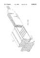
- FIG. 15is a rear view of a completed 5 ⁇ 6 connector (rows ⁇ columns) formed by juxtaposing three shielded pair modules arranged in side by side relationship within housing 70.
- Each module 90includes a pair of juxtaposed PCB's 31, 31' on which press-fit terminals (such as shield terminals) 37, 37', are mounted.
- Each PCB 31, 31'is held by an associated insulative cover 56, 56'.
- the covers 56, 56'have dove-tail ribs 65, 65' fitted within dove-tail slots 73 in the housing.
- the dotted squares 92represent the locations of the terminals 34, 34' and generally correspond to the location of the openings 85 in the face-plate 80 (FIG. 11).
- the contact pitch X existing between adjacent columns at the intermating face of the connectoralso exists at the board mounting interface at terminals 37.
- Each of these shielded pair modules 90carry five shielded pairs of terminals and terminal leads in the 5 ⁇ 6 configuration illustrated in FIG. 15.
- FIG. 16is a rear view of a connector essentially as illustrated in prior co-pending International Application Ser. No. PCT/US96/11214 filed Jul. 2, 1996.
- the PCB modules 30are arranged in the connector housing 70 so that all of the PCB assemblies 30 are oriented in the same way, for example, with the cover 56 disposed on the left-hand side and the PCB 31 disposed on the right-hand side.
- FIGS. 17a, 17b, and 17cillustrate connectors embodying an aspect of the present invention.
- FIG. 17aillustrates from a rear view one form of twinax connector having shielded pairs of terminals and terminal leads.
- the terminal pair modules 91are formed by placing the covers 56, 56 in back to back relationship with the PCB's 31, 31' forming the exterior surfaces of the module.
- the signal and ground traces 32, 32' and 33, 33', respectivelyare located in facing mirror-image relationship on the interior surfaces of the PCB's 31, 31', with the outer-shielding layers 38, 38' disposed outwardly.
- twinax pairs 93 of terminalsthat are substantially parallel through the conductor and have essentially identical electrical characteristics. These pairs are shown by the dotted enclosures 93 for the left-hand most module 91.
- FIG. 17bThe connector shown in FIG. 17b is essentially the same arrangement as that shown in FIG. 17a, with the exception that instead of two covers 56, 56', a single insulative member 57 is utilized to hold the opposed PCB's 31, 31'. In each of the modules 91 the outer surfaces of the member 57 are configured similarly to the interior surfaces of the covers 56, 56'.
- FIG. 17cessentially illustrates the arrangement previously discussed with respect to FIG. 15.
- a single multi-layer PCB 31"may be employed having a centrally located, substantially continuous central shield layer, with the signal and shielding traces formed on opposed sides of the 31" in mirror-image relationship.
- FIGS. 18a and 18bare schematic representations designed to illustrate the electrical differences between the FIGS. 17a-b type of connectors and the FIG. 17c type of connector.
- the pair of interconnection terminals 94are electrically isolated by a common shield S.
- each of the interconnections 94 of the pairare individually shielded. In either case, an electrically matched pair of interconnections are formed to maintain essentially a twinax relationship through the interconnection.
- FIG. 19illustrates an arrangement for cable connectors.
- FIG. 19shows a cover 100 for use with a circuit board generally of the type previously described.
- the upper portion of the cover 100is substantially similar to the cover 56 shown in the previous embodiments. It includes on its upper and lower surfaces dove-tail ribs 165 and 166 that are designed to be received in corresponding dove-tail grooves in a housing, such as housing 70 shown in FIG. 10.
- a printed circuit boardhas a plated through hole for receiving the locating lug 162.
- the locating ribs 163 and 164are the equivalent of locating ribs 63 and 64 shown in FIG. 6C and serve to locate the PCB in the same manner.
- the PCB assembly to be associated with the cover 100differs from those previously described essentially by the absence of press-fit terminals 35 and 37.
- the cover 100includes a retaining structure 102 for retaining a flexible conductor, for example, a cable formed of a plurality of individual wires.
- the retaining structure 102includes an opening 104 for receiving the cable.
- a suitable strain relief element or elementsmay be provided at the location of opening 104 to enhance cable retention.
- the retaining structure 102preferably includes a plurality of routing pegs 106 that are useful to separate individual wires that are to be attached to the PCB. Such individual wires are schematically illustrated by the dotted lines 108 in FIG. 19. The ends of the wires 108, 109 may be soldered to contact pads on the PCB that are coincident with the recesses 110 in the cover 100.
- the PCBis assembled to the cover 100 and the individual wires 108 are arranged between the pegs 106.
- the cable(not shown) includes one or more drain lines, which can be represented by the line 109, these drain lines can be soldered to the shielding structures of the printed circuit board such as traces 33, layer 36 and 38 by connection at an appropriate location, for example, the right hand at most location of the PCB that in the previous embodiment corresponds to the location of press-fit shield terminal 37.
- shielded pair modulesemploy two covers 100, one of which is a mirror-image of the other. Each one of a twisted wire pair is connected to corresponding traces on each of the printed circuit boards.
- each twisted pairhas an individual drain
- the drain wirecan be connected to an appropriate shielding trace 33.
- FIGS. 20a-20cillustrate the components of a typical cable connector.
- the connector illustratedis a twinax connector but other configurations are possible by varying the relative orientation and layout of the modules.
- this connectorthere are two mirror image PCB's 31 and 31' placed in back to back relationship with shielding layers placed next to each other.
- Signal wires 108are each attached to one of the conductive signal traces 32 on each of the PCB's 31 and 31', along a bottom edge of each PCB.
- conductors from each twisted pairwould be attached to corresponding signal traces on each of the PCB's 31 and 31'.
- a drain or shield 109is present in the cable, it can be secured to the shield portion 36 .
- the securing of the various wires to the PCB'sis accomplished by conventional means, such as soldering or welding.
- the shield traces 33 and shield portion 36are interconnected to the shield layers 38 and 38' by plated vias 112 and the plated location hole 39 as previously described.
- Covers 100 and 100'are secured onto the respective PCB's 31 and 31'.
- the retainer sections of each coversurround the ends of the wires attached to the PCB's 31 and 31'.
- the retaining sectionsinclude the pegs 106, which provide strain relief and wire support functions.
- the PCB's 31 and 31'may be held together by a conductive adhesive or may be closely held together by the effect of the dove tail ribs 165 and 165' and corresponding dove tail slots 73 and 77 in the housing 70, as the module is assembled in the housing 70 as shown in FIG. 20b.
- a plurality of modulesare arranged in the molded plastic housing 70, the interior surfaces of which may be metallized to provide additional shielding.
- the face plate 80is secured to housing 70 to form the completed right angle cable connector shown in FIG. 20c.
- FIGS. 21a-21cshow essentially the same elements illustrated in FIGS. 20a-20c with the exception that the PCB's 33 and 33' are configured to provide a cable connection end at the rear edge of the PCB's rather than the bottom edge.
- the insulating covers 100 and 100'are modified correspondingly to situate the cable retaining sections 102 and 102' at the rear edges of the PCB's.
- the coversinclude pegs 106 for providing support, organization, and strain relief.
- the covers 100 and 100'may be secured together at engaging edges along the PCB's and at the retaining sections, for example by adhesives or solvent or heat welding.
- the modulesare then inserted into housing 70 as shown in FIG. 21b and are retained in the housing as previously described.
- a completed straight connectoris formed by the insertion of a plurality of modules in side by side relationship into the housing 70 and securing a face plate 80 on the housing, as illustrated in FIG. 21c.
Landscapes
- Details Of Connecting Devices For Male And Female Coupling (AREA)
- Coupling Device And Connection With Printed Circuit (AREA)
Abstract
Description
Claims (37)
Priority Applications (8)
| Application Number | Priority Date | Filing Date | Title |
|---|---|---|---|
| US08/784,743US6083047A (en) | 1997-01-16 | 1997-01-16 | Modular electrical PCB assembly connector |
| CA002225151ACA2225151C (en) | 1997-01-07 | 1997-12-17 | Connector with integrated pcb assembly |
| EP97122940AEP0852414B1 (en) | 1997-01-07 | 1997-12-29 | Connector with integrated PCB assembly |
| DE69731719TDE69731719T2 (en) | 1997-01-07 | 1997-12-29 | Connector with integrated circuit board assembly |
| SG1998000014ASG71746A1 (en) | 1997-01-07 | 1998-01-02 | Connector with integrated pcb assembly |
| CN98104204ACN1190807A (en) | 1997-01-07 | 1998-01-06 | Connector with IC printed board assembly |
| TW087100146ATW385579B (en) | 1997-01-07 | 1998-01-07 | Connector with integrated PCB assembly |
| JP00177998AJP4565673B2 (en) | 1997-01-07 | 1998-01-07 | Connector with integrated PCB assembly |
Applications Claiming Priority (1)
| Application Number | Priority Date | Filing Date | Title |
|---|---|---|---|
| US08/784,743US6083047A (en) | 1997-01-16 | 1997-01-16 | Modular electrical PCB assembly connector |
Publications (1)
| Publication Number | Publication Date |
|---|---|
| US6083047Atrue US6083047A (en) | 2000-07-04 |
Family
ID=25133396
Family Applications (1)
| Application Number | Title | Priority Date | Filing Date |
|---|---|---|---|
| US08/784,743Expired - LifetimeUS6083047A (en) | 1997-01-07 | 1997-01-16 | Modular electrical PCB assembly connector |
Country Status (1)
| Country | Link |
|---|---|
| US (1) | US6083047A (en) |
Cited By (117)
| Publication number | Priority date | Publication date | Assignee | Title |
|---|---|---|---|---|
| US6171115B1 (en)* | 2000-02-03 | 2001-01-09 | Tyco Electronics Corporation | Electrical connector having circuit boards and keying for different types of circuit boards |
| US6227882B1 (en)* | 1997-10-01 | 2001-05-08 | Berg Technology, Inc. | Connector for electrical isolation in a condensed area |
| US6283792B1 (en)* | 2000-07-11 | 2001-09-04 | Bernard R. Tolmie | Extruded metallic electrical connector assembly and method of producing same |
| US6322379B1 (en)* | 1999-04-21 | 2001-11-27 | Fci Americas Technology, Inc. | Connector for electrical isolation in a condensed area |
| US6328602B1 (en)* | 1999-06-17 | 2001-12-11 | Nec Corporation | Connector with less crosstalk |
| US6343955B2 (en)* | 2000-03-29 | 2002-02-05 | Berg Technology, Inc. | Electrical connector with grounding system |
| USD453735S1 (en) | 2000-12-28 | 2002-02-19 | Hon Hai Precision Ind. Co., Ltd. | Electrical connector |
| US6386924B2 (en)* | 2000-03-31 | 2002-05-14 | Tyco Electronics Corporation | Connector assembly with stabilized modules |
| EP1229767A1 (en)* | 2001-02-05 | 2002-08-07 | Fci | Bus bar arrangement with an integrated printed circuit board |
| US6439930B1 (en)* | 2001-11-05 | 2002-08-27 | Hon Hai Precision Ind. Co., Ltd. | Electrical connector configured by wafers including moveable contacts |
| US6443740B1 (en)* | 1998-10-15 | 2002-09-03 | Fci Americas Technology, Inc. | Connector system |
| US6527588B2 (en)* | 1997-01-16 | 2003-03-04 | Fci Americas Technology, Inc. | Electrical connector with integrated PCB assembly |
| US6540522B2 (en) | 2001-04-26 | 2003-04-01 | Tyco Electronics Corporation | Electrical connector assembly for orthogonally mating circuit boards |
| US6544072B2 (en)* | 2001-06-12 | 2003-04-08 | Berg Technologies | Electrical connector with metallized polymeric housing |
| US6551140B2 (en)* | 2001-05-09 | 2003-04-22 | Hon Hai Precision Ind. Co., Ltd. | Electrical connector having differential pair terminals with equal length |
| US6554647B1 (en)* | 1997-02-07 | 2003-04-29 | Teradyne, Inc. | Differential signal electrical connectors |
| US20030092320A1 (en)* | 2001-11-12 | 2003-05-15 | Evans Robert F. | Connector for high-speed communications |
| US6565387B2 (en)* | 1999-06-30 | 2003-05-20 | Teradyne, Inc. | Modular electrical connector and connector system |
| EP1315245A1 (en)* | 2001-11-20 | 2003-05-28 | Fci | Surface-mounted right-angle electrical connector |
| US6579124B1 (en) | 1999-08-16 | 2003-06-17 | Tyco Electronics Logistics Ag | Shielded electrical connector |
| US20030119379A1 (en)* | 2001-11-28 | 2003-06-26 | Avery Hazelton P. | High-density connector assembly with isolation spacer |
| US20030129872A1 (en)* | 2002-01-07 | 2003-07-10 | Tolmie Bernard R. | Hybrid connector system and method |
| US6607401B1 (en)* | 1999-01-28 | 2003-08-19 | Berg Technology, Inc. | Electrical connector mateable in a plurality of orientations |
| US6612857B2 (en) | 2001-07-05 | 2003-09-02 | Bernard R. Tolmie | Electrical connector system and method having optical and/or cooling capability |
| US6612869B1 (en)* | 2002-05-21 | 2003-09-02 | Hon Hai Precision Ind. Co., Ltd. | High density interconnection system |
| US6623302B2 (en)* | 2000-12-21 | 2003-09-23 | Hon Hai Precision Ind. Co., Ltd. | Electrical connector having printed substrates therein electrically contacting conductive contacts thereof by solderless |
| US6634908B1 (en)* | 2002-05-30 | 2003-10-21 | Hon Hai Precision Ind. Co., Ltd. | High density electrical connector with improved grounding bus |
| US6638079B1 (en)* | 2002-05-21 | 2003-10-28 | Hon Hai Precision Ind. Co., Ltd. | Customizable electrical connector |
| US6638082B2 (en) | 2001-11-20 | 2003-10-28 | Fci Americas Technology, Inc. | Pin-grid-array electrical connector |
| US6638110B1 (en)* | 2002-05-22 | 2003-10-28 | Hon Hai Precision Ind. Co., Ltd. | High density electrical connector |
| US6641438B1 (en)* | 2002-06-07 | 2003-11-04 | Hon Hai Precision Ind. Co., Ltd. | High speed, high density backplane connector |
| US6645009B1 (en)* | 2002-06-04 | 2003-11-11 | Hon Hai Precision Ind. Co., Ltd. | High density electrical connector with lead-in device |
| US6645010B1 (en)* | 2002-06-07 | 2003-11-11 | Hon Hai Precision Ind. Co., Ltd. | High density electrical connector with improved grounding bus |
| WO2003094303A1 (en)* | 2002-05-06 | 2003-11-13 | Molex Incorporated | High-speed differential signal connector |
| US6655966B2 (en)* | 2002-03-19 | 2003-12-02 | Tyco Electronics Corporation | Modular connector with grounding interconnect |
| US6682369B1 (en)* | 2002-09-18 | 2004-01-27 | Hon Hai Precision Ind. Co., Ltd. | Electrical connector having retention system for precisely mounting plural boards therein |
| US20040018773A1 (en)* | 2002-07-29 | 2004-01-29 | Fci Americas Technology, Inc. | Printed circuit board assembly having a BGA connection |
| US6685510B1 (en)* | 2002-10-22 | 2004-02-03 | Hon Hai Precision Ind. Co., Ltd. | Electrical cable connector |
| US6695646B1 (en)* | 2002-10-18 | 2004-02-24 | Hon Hai Precision Ind. Co., Ltd. | Electrical connector having floatable chicklets |
| US20040038564A1 (en)* | 2002-06-21 | 2004-02-26 | Bi-Jian Yan | Electrical connector |
| US6705895B2 (en)* | 2002-04-25 | 2004-03-16 | Tyco Electronics Corporation | Orthogonal interface for connecting circuit boards carrying differential pairs |
| US6743050B1 (en)* | 2002-12-10 | 2004-06-01 | Hon Hai Precision Ind. Co., Ltd. | Cable assembly with latch mechanism |
| US6769935B2 (en)* | 2001-02-01 | 2004-08-03 | Teradyne, Inc. | Matrix connector |
| US6808399B2 (en) | 2002-12-02 | 2004-10-26 | Tyco Electronics Corporation | Electrical connector with wafers having split ground planes |
| US6824391B2 (en) | 2000-02-03 | 2004-11-30 | Tyco Electronics Corporation | Electrical connector having customizable circuit board wafers |
| US6843657B2 (en) | 2001-01-12 | 2005-01-18 | Litton Systems Inc. | High speed, high density interconnect system for differential and single-ended transmission applications |
| US20050020134A1 (en)* | 2003-07-24 | 2005-01-27 | Winings Clifford L. | Modular electrical connector |
| US6866518B1 (en) | 2003-09-23 | 2005-03-15 | Hon Hai Precision Ind. Co., Ltd. | Electrical interconnection between multiple printed circuit boards |
| US20050064736A1 (en)* | 2003-09-23 | 2005-03-24 | Korsunsky Iosif R. | Electrical connector for interconnecting two intersected printed circuit boards |
| US20050064737A1 (en)* | 2003-09-23 | 2005-03-24 | Korsunsky Iosif R. | Method for interconnecting multiple printed circuit boards |
| US6875031B1 (en) | 2003-12-05 | 2005-04-05 | Hon Hai Precision Ind. Co., Ltd. | Electrical connector with circuit board module |
| US6910897B2 (en) | 2001-01-12 | 2005-06-28 | Litton Systems, Inc. | Interconnection system |
| US20050180225A1 (en)* | 1994-06-20 | 2005-08-18 | Neomagic Corporation | Graphics Controller Integrated Circuit without Memory Interface |
| US6979202B2 (en) | 2001-01-12 | 2005-12-27 | Litton Systems, Inc. | High-speed electrical connector |
| US20050283974A1 (en)* | 2004-06-23 | 2005-12-29 | Richard Robert A | Methods of manufacturing an electrical connector incorporating passive circuit elements |
| US20060014433A1 (en)* | 2004-07-14 | 2006-01-19 | Consoli John J | Electrical connector with ESD protection |
| US20060121749A1 (en)* | 2004-12-02 | 2006-06-08 | Tyco Electronics Corporation | Noise canceling differential connector and footprint |
| EP1480292A3 (en)* | 2003-05-22 | 2006-08-02 | Tyco Electronics AMP K.K. | Connector assembly |
| US20070021004A1 (en)* | 2005-03-31 | 2007-01-25 | Laurx John C | High-density, robust connector with dielectric insert |
| US7309257B1 (en) | 2006-06-30 | 2007-12-18 | Fci Americas Technology, Inc. | Hinged leadframe assembly for an electrical connector |
| US20080003890A1 (en)* | 2006-06-30 | 2008-01-03 | Minich Steven E | Leadframe assembly staggering for electrical connectors |
| US20080045044A1 (en)* | 2006-08-15 | 2008-02-21 | Hon Hai Precision Ind. Co., Ltd. | Electrical interconnection between multiple printed circuit boards |
| US20080160837A1 (en)* | 2006-12-01 | 2008-07-03 | Siemon John A | Modular Connector With Reduced Termination Variability |
| US20080176460A1 (en)* | 2006-08-02 | 2008-07-24 | Fedder James L | Electrical terminal having improved insertion characteristics and electrical connector for use therewith |
| US7549897B2 (en) | 2006-08-02 | 2009-06-23 | Tyco Electronics Corporation | Electrical connector having improved terminal configuration |
| US20090176412A1 (en)* | 2008-01-07 | 2009-07-09 | Lear Corporation | Modular electrical connector |
| US20090191727A1 (en)* | 2008-01-29 | 2009-07-30 | Hon Hai Precision Ind. Co., Ltd. | Electrical connector having improved terminal module |
| US7591655B2 (en) | 2006-08-02 | 2009-09-22 | Tyco Electronics Corporation | Electrical connector having improved electrical characteristics |
| US20090298308A1 (en)* | 2004-06-23 | 2009-12-03 | Kenny William A | Electrical connector incorporating passive circuit elements |
| US7637777B1 (en) | 2008-10-13 | 2009-12-29 | Tyco Electronics Corporation | Connector assembly having a noise-reducing contact pattern |
| US20090325397A1 (en)* | 2008-06-30 | 2009-12-31 | Fujitsu Component Limited | Cable connector |
| US7670196B2 (en) | 2006-08-02 | 2010-03-02 | Tyco Electronics Corporation | Electrical terminal having tactile feedback tip and electrical connector for use therewith |
| US20100055933A1 (en)* | 2008-08-28 | 2010-03-04 | Molex Incorporated | High-density, robust connector |
| US20100093195A1 (en)* | 2008-10-13 | 2010-04-15 | Tyco Electronics Corporation | Connector assembly having multiple contact arrangements |
| US20100093189A1 (en)* | 2008-10-13 | 2010-04-15 | Tyco Electronics Corporation | Connector assembly having signal and coaxial contacts |
| US20100093193A1 (en)* | 2008-10-13 | 2010-04-15 | Tyco Electronics Corporation | Connector assembly having a compressive coupling member |
| US20100093209A1 (en)* | 2008-10-15 | 2010-04-15 | Hon Hai Precision Industry Co., Ltd. | Electrical connector assembly with improved resisting structure to ensure reliable contacting between ground shields thereof |
| US20100093194A1 (en)* | 2008-10-13 | 2010-04-15 | Tyco Electronics Corporation | Connector assembly with variable stack heights having power and signal contacts |
| US20100144172A1 (en)* | 2008-01-07 | 2010-06-10 | Lear Corporation | Electrical connector and heat sink |
| US20100240233A1 (en)* | 2009-03-19 | 2010-09-23 | Johnescu Douglas M | Electrical connector having ribbed ground plate |
| US20100303415A1 (en)* | 2009-04-23 | 2010-12-02 | Tyco Electronics Corporation | Connector assemblies and systems including flexible circuits |
| US7918683B1 (en) | 2010-03-24 | 2011-04-05 | Tyco Electronics Corporation | Connector assemblies and daughter card assemblies configured to engage each other along a side interface |
| US8142236B2 (en) | 2006-08-02 | 2012-03-27 | Tyco Electronics Corporation | Electrical connector having improved density and routing characteristics and related methods |
| US8210877B2 (en) | 2007-12-28 | 2012-07-03 | Fci | Modular connector |
| US8231415B2 (en) | 2009-07-10 | 2012-07-31 | Fci Americas Technology Llc | High speed backplane connector with impedance modification and skew correction |
| US8382524B2 (en) | 2010-05-21 | 2013-02-26 | Amphenol Corporation | Electrical connector having thick film layers |
| US8439704B2 (en)* | 2008-09-09 | 2013-05-14 | Molex Incorporated | Horizontally configured connector with edge card mounting structure |
| US8491313B2 (en) | 2011-02-02 | 2013-07-23 | Amphenol Corporation | Mezzanine connector |
| US8591257B2 (en) | 2011-11-17 | 2013-11-26 | Amphenol Corporation | Electrical connector having impedance matched intermediate connection points |
| US8734185B2 (en) | 2010-05-21 | 2014-05-27 | Amphenol Corporation | Electrical connector incorporating circuit elements |
| US20140295696A1 (en)* | 2013-04-02 | 2014-10-02 | Hon Hai Precision Industry Co., Ltd. | Electrical connector |
| US8864521B2 (en) | 2005-06-30 | 2014-10-21 | Amphenol Corporation | High frequency electrical connector |
| USD718253S1 (en) | 2012-04-13 | 2014-11-25 | Fci Americas Technology Llc | Electrical cable connector |
| US8905651B2 (en) | 2012-01-31 | 2014-12-09 | Fci | Dismountable optical coupling device |
| USD720698S1 (en) | 2013-03-15 | 2015-01-06 | Fci Americas Technology Llc | Electrical cable connector |
| US8944831B2 (en) | 2012-04-13 | 2015-02-03 | Fci Americas Technology Llc | Electrical connector having ribbed ground plate with engagement members |
| USD727268S1 (en) | 2012-04-13 | 2015-04-21 | Fci Americas Technology Llc | Vertical electrical connector |
| USD727852S1 (en) | 2012-04-13 | 2015-04-28 | Fci Americas Technology Llc | Ground shield for a right angle electrical connector |
| USD733662S1 (en) | 2013-01-25 | 2015-07-07 | Fci Americas Technology Llc | Connector housing for electrical connector |
| USD746236S1 (en) | 2012-07-11 | 2015-12-29 | Fci Americas Technology Llc | Electrical connector housing |
| US9257778B2 (en) | 2012-04-13 | 2016-02-09 | Fci Americas Technology | High speed electrical connector |
| US9543703B2 (en) | 2012-07-11 | 2017-01-10 | Fci Americas Technology Llc | Electrical connector with reduced stack height |
| US20170170583A1 (en)* | 2015-12-14 | 2017-06-15 | Ge Aviation Systems Limited | Distributing wiring board connections |
| US20190131729A1 (en)* | 2017-10-31 | 2019-05-02 | Seagate Technology Llc | Pcb mounted cable apparatus and methods thereof |
| US10833455B2 (en)* | 2018-12-28 | 2020-11-10 | Fu Ding Precision Industrial (Zhenghou) Co., Ltd. | Contact module having double-sided arranged contacts with insulator and respective equal length differential pair thereof |
| US11444397B2 (en) | 2015-07-07 | 2022-09-13 | Amphenol Fci Asia Pte. Ltd. | Electrical connector with cavity between terminals |
| US11469553B2 (en) | 2020-01-27 | 2022-10-11 | Fci Usa Llc | High speed connector |
| US11522310B2 (en) | 2012-08-22 | 2022-12-06 | Amphenol Corporation | High-frequency electrical connector |
| US11539171B2 (en) | 2016-08-23 | 2022-12-27 | Amphenol Corporation | Connector configurable for high performance |
| US11715914B2 (en) | 2014-01-22 | 2023-08-01 | Amphenol Corporation | High speed, high density electrical connector with shielded signal paths |
| US11757224B2 (en) | 2010-05-07 | 2023-09-12 | Amphenol Corporation | High performance cable connector |
| US11757215B2 (en) | 2018-09-26 | 2023-09-12 | Amphenol East Asia Electronic Technology (Shenzhen) Co., Ltd. | High speed electrical connector and printed circuit board thereof |
| US11799246B2 (en) | 2020-01-27 | 2023-10-24 | Fci Usa Llc | High speed connector |
| US11817655B2 (en) | 2020-09-25 | 2023-11-14 | Amphenol Commercial Products (Chengdu) Co., Ltd. | Compact, high speed electrical connector |
| US11942716B2 (en) | 2020-09-22 | 2024-03-26 | Amphenol Commercial Products (Chengdu) Co., Ltd. | High speed electrical connector |
| US12300920B2 (en) | 2021-08-13 | 2025-05-13 | Amphenol Commercial Products (Chengdu) Co., Ltd. | High performance card edge connector for high bandwidth transmission |
| US12300936B2 (en) | 2019-02-19 | 2025-05-13 | Amphenol Corporation | High speed connector |
Citations (19)
| Publication number | Priority date | Publication date | Assignee | Title |
|---|---|---|---|---|
| US4338717A (en)* | 1980-09-02 | 1982-07-13 | Augat Inc. | Method for fabricating a light emitting diode display socket |
| US4571014A (en)* | 1984-05-02 | 1986-02-18 | At&T Bell Laboratories | High frequency modular connector |
| US4689721A (en)* | 1986-01-10 | 1987-08-25 | Trw Inc. | Dual printed circuit board module |
| US4705332A (en)* | 1985-08-05 | 1987-11-10 | Criton Technologies | High density, controlled impedance connectors |
| US4806107A (en)* | 1987-10-16 | 1989-02-21 | American Telephone And Telegraph Company, At&T Bell Laboratories | High frequency connector |
| US4861272A (en)* | 1988-03-31 | 1989-08-29 | E. I. Du Pont De Nemours And Company | Impedance controlled connector interface |
| US4975084A (en)* | 1988-10-17 | 1990-12-04 | Amp Incorporated | Electrical connector system |
| EP0442643A2 (en)* | 1990-02-13 | 1991-08-21 | W.L. GORE & ASSOCIATES (UK) LTD | Shielded connector |
| US5055069A (en)* | 1990-06-08 | 1991-10-08 | E. I. Du Pont De Nemours And Company | Connectors with ground structure |
| US5066236A (en)* | 1989-10-10 | 1991-11-19 | Amp Incorporated | Impedance matched backplane connector |
| US5104341A (en)* | 1989-12-20 | 1992-04-14 | Amp Incorporated | Shielded backplane connector |
| US5122065A (en)* | 1991-08-12 | 1992-06-16 | International Business Machines Corp. | Input output connector with coaxial shielding and strain relief |
| US5174770A (en)* | 1990-11-15 | 1992-12-29 | Amp Incorporated | Multicontact connector for signal transmission |
| US5454738A (en)* | 1993-10-05 | 1995-10-03 | Thomas & Betts Corporation | Electrical connector having reduced cross-talk |
| US5460533A (en)* | 1992-05-11 | 1995-10-24 | The Whitaker Corporation | Cable backpanel interconnection |
| US5522727A (en)* | 1993-09-17 | 1996-06-04 | Japan Aviation Electronics Industry, Limited | Electrical angle connector of a printed circuit board type having a plurality of connecting conductive strips of a common length |
| EP0752739A1 (en)* | 1995-07-03 | 1997-01-08 | Berg Electronics Manufacturing B.V. | Connector, preferably a right angle connector, with integrated pcb assembly |
| US5605477A (en)* | 1995-01-13 | 1997-02-25 | The Whitaker Corporation | Flexible etched circuit assembly |
| US5664968A (en)* | 1996-03-29 | 1997-09-09 | The Whitaker Corporation | Connector assembly with shielded modules |
- 1997
- 1997-01-16USUS08/784,743patent/US6083047A/ennot_activeExpired - Lifetime
Patent Citations (21)
| Publication number | Priority date | Publication date | Assignee | Title |
|---|---|---|---|---|
| US4338717A (en)* | 1980-09-02 | 1982-07-13 | Augat Inc. | Method for fabricating a light emitting diode display socket |
| US4571014A (en)* | 1984-05-02 | 1986-02-18 | At&T Bell Laboratories | High frequency modular connector |
| US4705332A (en)* | 1985-08-05 | 1987-11-10 | Criton Technologies | High density, controlled impedance connectors |
| US4689721A (en)* | 1986-01-10 | 1987-08-25 | Trw Inc. | Dual printed circuit board module |
| US4806107A (en)* | 1987-10-16 | 1989-02-21 | American Telephone And Telegraph Company, At&T Bell Laboratories | High frequency connector |
| US4861272A (en)* | 1988-03-31 | 1989-08-29 | E. I. Du Pont De Nemours And Company | Impedance controlled connector interface |
| US4975084A (en)* | 1988-10-17 | 1990-12-04 | Amp Incorporated | Electrical connector system |
| US5066236A (en)* | 1989-10-10 | 1991-11-19 | Amp Incorporated | Impedance matched backplane connector |
| US5104341A (en)* | 1989-12-20 | 1992-04-14 | Amp Incorporated | Shielded backplane connector |
| EP0442643A2 (en)* | 1990-02-13 | 1991-08-21 | W.L. GORE & ASSOCIATES (UK) LTD | Shielded connector |
| US5055069A (en)* | 1990-06-08 | 1991-10-08 | E. I. Du Pont De Nemours And Company | Connectors with ground structure |
| US5174770A (en)* | 1990-11-15 | 1992-12-29 | Amp Incorporated | Multicontact connector for signal transmission |
| US5122065A (en)* | 1991-08-12 | 1992-06-16 | International Business Machines Corp. | Input output connector with coaxial shielding and strain relief |
| US5460533A (en)* | 1992-05-11 | 1995-10-24 | The Whitaker Corporation | Cable backpanel interconnection |
| US5522727A (en)* | 1993-09-17 | 1996-06-04 | Japan Aviation Electronics Industry, Limited | Electrical angle connector of a printed circuit board type having a plurality of connecting conductive strips of a common length |
| US5454738A (en)* | 1993-10-05 | 1995-10-03 | Thomas & Betts Corporation | Electrical connector having reduced cross-talk |
| US5470244A (en)* | 1993-10-05 | 1995-11-28 | Thomas & Betts Corporation | Electrical connector having reduced cross-talk |
| US5605477A (en)* | 1995-01-13 | 1997-02-25 | The Whitaker Corporation | Flexible etched circuit assembly |
| EP0752739A1 (en)* | 1995-07-03 | 1997-01-08 | Berg Electronics Manufacturing B.V. | Connector, preferably a right angle connector, with integrated pcb assembly |
| WO1997002627A1 (en)* | 1995-07-03 | 1997-01-23 | Berg Technology, Inc. | Connector, preferably a right angle connector, with integrated pcb assembly |
| US5664968A (en)* | 1996-03-29 | 1997-09-09 | The Whitaker Corporation | Connector assembly with shielded modules |
Non-Patent Citations (2)
| Title |
|---|
| "Field-Based Design of a New High Pincount Board Connector for High Data Transmission" By H. Katzier, B.-M Keller, Peter Pagnin, Dirk Michel, 1996 Electronic Components and Technology Conference, pp. 456-459, publication date May 28, 1996. |
| Field Based Design of a New High Pincount Board Connector for High Data Transmission By H. Katzier, B. M Keller, Peter Pagnin, Dirk Michel, 1996 Electronic Components and Technology Conference, pp. 456 459, publication date May 28, 1996.* |
Cited By (223)
| Publication number | Priority date | Publication date | Assignee | Title |
|---|---|---|---|---|
| US20050180225A1 (en)* | 1994-06-20 | 2005-08-18 | Neomagic Corporation | Graphics Controller Integrated Circuit without Memory Interface |
| US6527588B2 (en)* | 1997-01-16 | 2003-03-04 | Fci Americas Technology, Inc. | Electrical connector with integrated PCB assembly |
| US6554647B1 (en)* | 1997-02-07 | 2003-04-29 | Teradyne, Inc. | Differential signal electrical connectors |
| US6227882B1 (en)* | 1997-10-01 | 2001-05-08 | Berg Technology, Inc. | Connector for electrical isolation in a condensed area |
| US6443740B1 (en)* | 1998-10-15 | 2002-09-03 | Fci Americas Technology, Inc. | Connector system |
| US6607401B1 (en)* | 1999-01-28 | 2003-08-19 | Berg Technology, Inc. | Electrical connector mateable in a plurality of orientations |
| US6322379B1 (en)* | 1999-04-21 | 2001-11-27 | Fci Americas Technology, Inc. | Connector for electrical isolation in a condensed area |
| US6328602B1 (en)* | 1999-06-17 | 2001-12-11 | Nec Corporation | Connector with less crosstalk |
| US6565387B2 (en)* | 1999-06-30 | 2003-05-20 | Teradyne, Inc. | Modular electrical connector and connector system |
| US6579124B1 (en) | 1999-08-16 | 2003-06-17 | Tyco Electronics Logistics Ag | Shielded electrical connector |
| US6171115B1 (en)* | 2000-02-03 | 2001-01-09 | Tyco Electronics Corporation | Electrical connector having circuit boards and keying for different types of circuit boards |
| US6824391B2 (en) | 2000-02-03 | 2004-11-30 | Tyco Electronics Corporation | Electrical connector having customizable circuit board wafers |
| US6364710B1 (en)* | 2000-03-29 | 2002-04-02 | Berg Technology, Inc. | Electrical connector with grounding system |
| US6343955B2 (en)* | 2000-03-29 | 2002-02-05 | Berg Technology, Inc. | Electrical connector with grounding system |
| US6386924B2 (en)* | 2000-03-31 | 2002-05-14 | Tyco Electronics Corporation | Connector assembly with stabilized modules |
| US6283792B1 (en)* | 2000-07-11 | 2001-09-04 | Bernard R. Tolmie | Extruded metallic electrical connector assembly and method of producing same |
| US6623302B2 (en)* | 2000-12-21 | 2003-09-23 | Hon Hai Precision Ind. Co., Ltd. | Electrical connector having printed substrates therein electrically contacting conductive contacts thereof by solderless |
| USD453735S1 (en) | 2000-12-28 | 2002-02-19 | Hon Hai Precision Ind. Co., Ltd. | Electrical connector |
| US6979202B2 (en) | 2001-01-12 | 2005-12-27 | Litton Systems, Inc. | High-speed electrical connector |
| US6843657B2 (en) | 2001-01-12 | 2005-01-18 | Litton Systems Inc. | High speed, high density interconnect system for differential and single-ended transmission applications |
| US6910897B2 (en) | 2001-01-12 | 2005-06-28 | Litton Systems, Inc. | Interconnection system |
| US7056128B2 (en) | 2001-01-12 | 2006-06-06 | Litton Systems, Inc. | High speed, high density interconnect system for differential and single-ended transmission systems |
| US7101191B2 (en) | 2001-01-12 | 2006-09-05 | Winchester Electronics Corporation | High speed electrical connector |
| US7019984B2 (en) | 2001-01-12 | 2006-03-28 | Litton Systems, Inc. | Interconnection system |
| US6769935B2 (en)* | 2001-02-01 | 2004-08-03 | Teradyne, Inc. | Matrix connector |
| EP1229767A1 (en)* | 2001-02-05 | 2002-08-07 | Fci | Bus bar arrangement with an integrated printed circuit board |
| FR2820602A1 (en)* | 2001-02-05 | 2002-08-09 | Fci Pontarlier | BUS BAR CONDUCTOR WITH INTEGRATED PRINTED CIRCUIT PLATE |
| US6540522B2 (en) | 2001-04-26 | 2003-04-01 | Tyco Electronics Corporation | Electrical connector assembly for orthogonally mating circuit boards |
| US6551140B2 (en)* | 2001-05-09 | 2003-04-22 | Hon Hai Precision Ind. Co., Ltd. | Electrical connector having differential pair terminals with equal length |
| US6544072B2 (en)* | 2001-06-12 | 2003-04-08 | Berg Technologies | Electrical connector with metallized polymeric housing |
| US6612857B2 (en) | 2001-07-05 | 2003-09-02 | Bernard R. Tolmie | Electrical connector system and method having optical and/or cooling capability |
| US6439930B1 (en)* | 2001-11-05 | 2002-08-27 | Hon Hai Precision Ind. Co., Ltd. | Electrical connector configured by wafers including moveable contacts |
| US6508675B1 (en)* | 2001-11-05 | 2003-01-21 | Hon Hai Precision Ind. Co., Ltd. | Electrical connector configured by wafers including moveable contacts |
| US20050118869A1 (en)* | 2001-11-12 | 2005-06-02 | Fci Americas Technology, Inc. | Connector for high-speed communications |
| US6848944B2 (en)* | 2001-11-12 | 2005-02-01 | Fci Americas Technology, Inc. | Connector for high-speed communications |
| US20030092320A1 (en)* | 2001-11-12 | 2003-05-15 | Evans Robert F. | Connector for high-speed communications |
| US7310875B2 (en) | 2001-11-12 | 2007-12-25 | Fci Americas Technology, Inc. | Connector for high-speed communications |
| EP1315245A1 (en)* | 2001-11-20 | 2003-05-28 | Fci | Surface-mounted right-angle electrical connector |
| US6666693B2 (en) | 2001-11-20 | 2003-12-23 | Fci Americas Technology, Inc. | Surface-mounted right-angle electrical connector |
| US6638082B2 (en) | 2001-11-20 | 2003-10-28 | Fci Americas Technology, Inc. | Pin-grid-array electrical connector |
| US20030119379A1 (en)* | 2001-11-28 | 2003-06-26 | Avery Hazelton P. | High-density connector assembly with isolation spacer |
| US20030124910A1 (en)* | 2001-11-28 | 2003-07-03 | Nelson Richard A. | High-density connector assembly with improved mating capability |
| US6851980B2 (en) | 2001-11-28 | 2005-02-08 | Molex Incorporated | High-density connector assembly with improved mating capability |
| WO2003047039A3 (en)* | 2001-11-28 | 2003-07-10 | Molex Inc | Interstitial ground assembly for connector |
| US6805587B2 (en) | 2001-11-28 | 2004-10-19 | Molex Incorporated | High-density connector assembly with isolation spacer |
| US6692305B2 (en) | 2001-11-28 | 2004-02-17 | Molex Incorporated | Flexural connector cover assembly mounting apparatus |
| US6746278B2 (en) | 2001-11-28 | 2004-06-08 | Molex Incorporated | Interstitial ground assembly for connector |
| US6749468B2 (en) | 2001-11-28 | 2004-06-15 | Molex Incorporated | High-density connector assembly mounting apparatus |
| US20030129872A1 (en)* | 2002-01-07 | 2003-07-10 | Tolmie Bernard R. | Hybrid connector system and method |
| US6821146B2 (en) | 2002-01-07 | 2004-11-23 | Bernard R. Tolmie | Hybrid connector system and method |
| US6655966B2 (en)* | 2002-03-19 | 2003-12-02 | Tyco Electronics Corporation | Modular connector with grounding interconnect |
| CN100334779C (en)* | 2002-03-19 | 2007-08-29 | 蒂科电子公司 | Ground Interconnect Modular Connectors |
| US6705895B2 (en)* | 2002-04-25 | 2004-03-16 | Tyco Electronics Corporation | Orthogonal interface for connecting circuit boards carrying differential pairs |
| US20040161974A1 (en)* | 2002-05-06 | 2004-08-19 | Lang Harold Keith | High-speed differential signal connector particularly suitable for docking applications |
| US6918789B2 (en) | 2002-05-06 | 2005-07-19 | Molex Incorporated | High-speed differential signal connector particularly suitable for docking applications |
| US20040038590A1 (en)* | 2002-05-06 | 2004-02-26 | Lang Harold Keith | High-speed differential signal connector with interstitial ground aspect |
| WO2003094303A1 (en)* | 2002-05-06 | 2003-11-13 | Molex Incorporated | High-speed differential signal connector |
| US6848917B2 (en) | 2002-05-06 | 2005-02-01 | Molex Incorporated | High-speed differential signal connector with interstitial ground aspect |
| CN100576651C (en)* | 2002-05-06 | 2009-12-30 | 莫莱克斯公司 | High Speed Differential Signal Connectors |
| US6612869B1 (en)* | 2002-05-21 | 2003-09-02 | Hon Hai Precision Ind. Co., Ltd. | High density interconnection system |
| US6638079B1 (en)* | 2002-05-21 | 2003-10-28 | Hon Hai Precision Ind. Co., Ltd. | Customizable electrical connector |
| US6663427B1 (en)* | 2002-05-22 | 2003-12-16 | Hon Hai Precision Ind. Co., Ltd. | High density electrical connector assembly |
| US6638110B1 (en)* | 2002-05-22 | 2003-10-28 | Hon Hai Precision Ind. Co., Ltd. | High density electrical connector |
| US6652319B1 (en)* | 2002-05-22 | 2003-11-25 | Hon Hai Precision Ind. Co., Ltd. | High speed connector with matched impedance |
| US20030220019A1 (en)* | 2002-05-22 | 2003-11-27 | Billman Timothy B. | High density electrical connector assembly |
| US6634908B1 (en)* | 2002-05-30 | 2003-10-21 | Hon Hai Precision Ind. Co., Ltd. | High density electrical connector with improved grounding bus |
| US6645009B1 (en)* | 2002-06-04 | 2003-11-11 | Hon Hai Precision Ind. Co., Ltd. | High density electrical connector with lead-in device |
| US6641438B1 (en)* | 2002-06-07 | 2003-11-04 | Hon Hai Precision Ind. Co., Ltd. | High speed, high density backplane connector |
| US6645010B1 (en)* | 2002-06-07 | 2003-11-11 | Hon Hai Precision Ind. Co., Ltd. | High density electrical connector with improved grounding bus |
| US20040038564A1 (en)* | 2002-06-21 | 2004-02-26 | Bi-Jian Yan | Electrical connector |
| US20060128184A1 (en)* | 2002-07-29 | 2006-06-15 | Fci Americas Technology, Inc. | Printed circuit board assembly having a BGA connection |
| US7413450B2 (en) | 2002-07-29 | 2008-08-19 | Fci Americas Technology, Inc. | Printed circuit board assembly having a BGA connection |
| US20040018773A1 (en)* | 2002-07-29 | 2004-01-29 | Fci Americas Technology, Inc. | Printed circuit board assembly having a BGA connection |
| US6682369B1 (en)* | 2002-09-18 | 2004-01-27 | Hon Hai Precision Ind. Co., Ltd. | Electrical connector having retention system for precisely mounting plural boards therein |
| US6695646B1 (en)* | 2002-10-18 | 2004-02-24 | Hon Hai Precision Ind. Co., Ltd. | Electrical connector having floatable chicklets |
| US6790089B2 (en)* | 2002-10-22 | 2004-09-14 | Hon Hai Precision Ind. Co., Ltd | Cable assembly |
| US6699072B1 (en)* | 2002-10-22 | 2004-03-02 | Hon Hai Precisionind Co., Ltd. | Cable assembly |
| US20040077228A1 (en)* | 2002-10-22 | 2004-04-22 | Jerry Wu | Cable assembly |
| US6685510B1 (en)* | 2002-10-22 | 2004-02-03 | Hon Hai Precision Ind. Co., Ltd. | Electrical cable connector |
| US6699073B1 (en)* | 2002-10-22 | 2004-03-02 | Hon Hai Precision Ind. Co., Ltd. | Cable assembly |
| US6808399B2 (en) | 2002-12-02 | 2004-10-26 | Tyco Electronics Corporation | Electrical connector with wafers having split ground planes |
| US20040110411A1 (en)* | 2002-12-10 | 2004-06-10 | Jerry Wu | Cable assembly with pull tab |
| US20040110420A1 (en)* | 2002-12-10 | 2004-06-10 | Jerry Wu | Cable assembly with latch mechanism |
| US6743050B1 (en)* | 2002-12-10 | 2004-06-01 | Hon Hai Precision Ind. Co., Ltd. | Cable assembly with latch mechanism |
| KR100851712B1 (en)* | 2003-05-22 | 2008-08-11 | 타이코 일렉트로닉스 에이엠피 케이.케이. | Connector assembly |
| CN100401595C (en)* | 2003-05-22 | 2008-07-09 | 安普泰科电子有限公司 | connector assembly |
| EP1480292A3 (en)* | 2003-05-22 | 2006-08-02 | Tyco Electronics AMP K.K. | Connector assembly |
| US20050020134A1 (en)* | 2003-07-24 | 2005-01-27 | Winings Clifford L. | Modular electrical connector |
| WO2005011068A3 (en)* | 2003-07-24 | 2005-04-14 | Fci Americas Technology Inc | Modular electrical connector |
| US7059907B2 (en)* | 2003-07-24 | 2006-06-13 | Fci Americas Technology, Inc. | Modular electrical connector |
| US6918775B2 (en) | 2003-09-23 | 2005-07-19 | Hon Hai Precision Ind. Co., Ltd. | Method for interconnecting multiple printed circuit boards |
| US6923655B2 (en) | 2003-09-23 | 2005-08-02 | Hon Hai Precision Ind. Co., Ltd. | Electrical connector for interconnecting two intersected printed circuit boards |
| US20050064736A1 (en)* | 2003-09-23 | 2005-03-24 | Korsunsky Iosif R. | Electrical connector for interconnecting two intersected printed circuit boards |
| US6866518B1 (en) | 2003-09-23 | 2005-03-15 | Hon Hai Precision Ind. Co., Ltd. | Electrical interconnection between multiple printed circuit boards |
| US20050064737A1 (en)* | 2003-09-23 | 2005-03-24 | Korsunsky Iosif R. | Method for interconnecting multiple printed circuit boards |
| US20050064733A1 (en)* | 2003-09-23 | 2005-03-24 | Korsunsky Iosif R. | Electrical interconnection between multiple printed circuit boards |
| US6875031B1 (en) | 2003-12-05 | 2005-04-05 | Hon Hai Precision Ind. Co., Ltd. | Electrical connector with circuit board module |
| US8123563B2 (en) | 2004-06-23 | 2012-02-28 | Amphenol Corporation | Electrical connector incorporating passive circuit elements |
| US20090298308A1 (en)* | 2004-06-23 | 2009-12-03 | Kenny William A | Electrical connector incorporating passive circuit elements |
| US20050283974A1 (en)* | 2004-06-23 | 2005-12-29 | Richard Robert A | Methods of manufacturing an electrical connector incorporating passive circuit elements |
| US7887371B2 (en) | 2004-06-23 | 2011-02-15 | Amphenol Corporation | Electrical connector incorporating passive circuit elements |
| US7044794B2 (en) | 2004-07-14 | 2006-05-16 | Tyco Electronics Corporation | Electrical connector with ESD protection |
| US20060014433A1 (en)* | 2004-07-14 | 2006-01-19 | Consoli John J | Electrical connector with ESD protection |
| US20060121749A1 (en)* | 2004-12-02 | 2006-06-08 | Tyco Electronics Corporation | Noise canceling differential connector and footprint |
| US7207807B2 (en) | 2004-12-02 | 2007-04-24 | Tyco Electronics Corporation | Noise canceling differential connector and footprint |
| US7553190B2 (en)* | 2005-03-31 | 2009-06-30 | Molex Incorporated | High-density, robust connector with dielectric insert |
| US20070021004A1 (en)* | 2005-03-31 | 2007-01-25 | Laurx John C | High-density, robust connector with dielectric insert |
| US8864521B2 (en) | 2005-06-30 | 2014-10-21 | Amphenol Corporation | High frequency electrical connector |
| US9219335B2 (en) | 2005-06-30 | 2015-12-22 | Amphenol Corporation | High frequency electrical connector |
| US9705255B2 (en) | 2005-06-30 | 2017-07-11 | Amphenol Corporation | High frequency electrical connector |
| US7597593B2 (en) | 2006-06-30 | 2009-10-06 | Fci Americas Technology, Inc. | Leadframe assembly staggering for electrical connectors |
| WO2008005117A3 (en)* | 2006-06-30 | 2008-06-26 | Fci Americas Technology Inc | Leadframe assembly staggering for electrical connectors |
| US7387535B2 (en) | 2006-06-30 | 2008-06-17 | Fci Americas Technology, Inc. | Hinged leadframe assembly for an electrical connector |
| US7318757B1 (en)* | 2006-06-30 | 2008-01-15 | Fci Americas Technology, Inc. | Leadframe assembly staggering for electrical connectors |
| US20080003878A1 (en)* | 2006-06-30 | 2008-01-03 | Minich Steven E | Hinged leadframe assembly for an electrical connector |
| US20080003879A1 (en)* | 2006-06-30 | 2008-01-03 | Fci Americas Technology, Inc. | Hinged leadframe assembly for an electrical connector |
| US20080003890A1 (en)* | 2006-06-30 | 2008-01-03 | Minich Steven E | Leadframe assembly staggering for electrical connectors |
| US7309257B1 (en) | 2006-06-30 | 2007-12-18 | Fci Americas Technology, Inc. | Hinged leadframe assembly for an electrical connector |
| US8142236B2 (en) | 2006-08-02 | 2012-03-27 | Tyco Electronics Corporation | Electrical connector having improved density and routing characteristics and related methods |
| US7789716B2 (en) | 2006-08-02 | 2010-09-07 | Tyco Electronics Corporation | Electrical connector having improved terminal configuration |
| US7549897B2 (en) | 2006-08-02 | 2009-06-23 | Tyco Electronics Corporation | Electrical connector having improved terminal configuration |
| US7591655B2 (en) | 2006-08-02 | 2009-09-22 | Tyco Electronics Corporation | Electrical connector having improved electrical characteristics |
| US20080176460A1 (en)* | 2006-08-02 | 2008-07-24 | Fedder James L | Electrical terminal having improved insertion characteristics and electrical connector for use therewith |
| US7753742B2 (en) | 2006-08-02 | 2010-07-13 | Tyco Electronics Corporation | Electrical terminal having improved insertion characteristics and electrical connector for use therewith |
| US7670196B2 (en) | 2006-08-02 | 2010-03-02 | Tyco Electronics Corporation | Electrical terminal having tactile feedback tip and electrical connector for use therewith |
| US7438556B2 (en) | 2006-08-15 | 2008-10-21 | Hon Hai Precision Ind. Co., Ltd. | Electrical interconnection between multiple printed circuit boards |
| US20080045044A1 (en)* | 2006-08-15 | 2008-02-21 | Hon Hai Precision Ind. Co., Ltd. | Electrical interconnection between multiple printed circuit boards |
| US20100003863A1 (en)* | 2006-12-01 | 2010-01-07 | The Siemon Company | Modular Connector With Reduced Termination Variability |
| WO2008069968A3 (en)* | 2006-12-01 | 2008-09-25 | Siemon Co | Modular connector with reduced termination variability |
| CN101595536B (en)* | 2006-12-01 | 2013-03-06 | 西蒙公司 | Modular connector with reduced termination variability |
| US7980899B2 (en) | 2006-12-01 | 2011-07-19 | The Siemon Company | Modular connector with reduced termination variability |
| US20080160837A1 (en)* | 2006-12-01 | 2008-07-03 | Siemon John A | Modular Connector With Reduced Termination Variability |
| US7604515B2 (en) | 2006-12-01 | 2009-10-20 | The Siemon Company | Modular connector with reduced termination variability |
| US8210877B2 (en) | 2007-12-28 | 2012-07-03 | Fci | Modular connector |
| US8038465B2 (en) | 2008-01-07 | 2011-10-18 | Lear Corporation | Electrical connector and heat sink |
| US20090176412A1 (en)* | 2008-01-07 | 2009-07-09 | Lear Corporation | Modular electrical connector |
| US20100144172A1 (en)* | 2008-01-07 | 2010-06-10 | Lear Corporation | Electrical connector and heat sink |
| US7713096B2 (en) | 2008-01-07 | 2010-05-11 | Lear Corporation | Modular electrical connector |
| US20090191727A1 (en)* | 2008-01-29 | 2009-07-30 | Hon Hai Precision Ind. Co., Ltd. | Electrical connector having improved terminal module |
| US7922520B2 (en)* | 2008-06-30 | 2011-04-12 | Fujitsu Component Limited | Cable connector including intermediary interconnection board |
| US20090325397A1 (en)* | 2008-06-30 | 2009-12-31 | Fujitsu Component Limited | Cable connector |
| US20100055933A1 (en)* | 2008-08-28 | 2010-03-04 | Molex Incorporated | High-density, robust connector |
| US7931474B2 (en)* | 2008-08-28 | 2011-04-26 | Molex Incorporated | High-density, robust connector |
| US9748713B2 (en) | 2008-09-09 | 2017-08-29 | Molex, Llc | Horizontally configured connector |
| US8439704B2 (en)* | 2008-09-09 | 2013-05-14 | Molex Incorporated | Horizontally configured connector with edge card mounting structure |
| US9461392B2 (en) | 2008-09-09 | 2016-10-04 | Molex, Llc | Vertically configured connector |
| US20100093194A1 (en)* | 2008-10-13 | 2010-04-15 | Tyco Electronics Corporation | Connector assembly with variable stack heights having power and signal contacts |
| US7736183B2 (en) | 2008-10-13 | 2010-06-15 | Tyco Electronics Corporation | Connector assembly with variable stack heights having power and signal contacts |
| US7740489B2 (en) | 2008-10-13 | 2010-06-22 | Tyco Electronics Corporation | Connector assembly having a compressive coupling member |
| US7896698B2 (en) | 2008-10-13 | 2011-03-01 | Tyco Electronics Corporation | Connector assembly having multiple contact arrangements |
| US8070514B2 (en) | 2008-10-13 | 2011-12-06 | Tyco Electronics Corporation | Connector assembly having multiple contact arrangements |
| US7637777B1 (en) | 2008-10-13 | 2009-12-29 | Tyco Electronics Corporation | Connector assembly having a noise-reducing contact pattern |
| US20100093193A1 (en)* | 2008-10-13 | 2010-04-15 | Tyco Electronics Corporation | Connector assembly having a compressive coupling member |
| US20100093189A1 (en)* | 2008-10-13 | 2010-04-15 | Tyco Electronics Corporation | Connector assembly having signal and coaxial contacts |
| US20100093195A1 (en)* | 2008-10-13 | 2010-04-15 | Tyco Electronics Corporation | Connector assembly having multiple contact arrangements |
| US7867032B2 (en) | 2008-10-13 | 2011-01-11 | Tyco Electronics Corporation | Connector assembly having signal and coaxial contacts |
| US20110021077A1 (en)* | 2008-10-13 | 2011-01-27 | Tyco Electronics Corporation | Connector assembly having multiple contact arrangements |
| US20100093209A1 (en)* | 2008-10-15 | 2010-04-15 | Hon Hai Precision Industry Co., Ltd. | Electrical connector assembly with improved resisting structure to ensure reliable contacting between ground shields thereof |
| US10720721B2 (en) | 2009-03-19 | 2020-07-21 | Fci Usa Llc | Electrical connector having ribbed ground plate |
| US8366485B2 (en) | 2009-03-19 | 2013-02-05 | Fci Americas Technology Llc | Electrical connector having ribbed ground plate |
| US9461410B2 (en) | 2009-03-19 | 2016-10-04 | Fci Americas Technology Llc | Electrical connector having ribbed ground plate |
| US9048583B2 (en) | 2009-03-19 | 2015-06-02 | Fci Americas Technology Llc | Electrical connector having ribbed ground plate |
| US10096921B2 (en) | 2009-03-19 | 2018-10-09 | Fci Usa Llc | Electrical connector having ribbed ground plate |
| US20100240233A1 (en)* | 2009-03-19 | 2010-09-23 | Johnescu Douglas M | Electrical connector having ribbed ground plate |
| US8113851B2 (en) | 2009-04-23 | 2012-02-14 | Tyco Electronics Corporation | Connector assemblies and systems including flexible circuits |
| US20100303415A1 (en)* | 2009-04-23 | 2010-12-02 | Tyco Electronics Corporation | Connector assemblies and systems including flexible circuits |
| US8231415B2 (en) | 2009-07-10 | 2012-07-31 | Fci Americas Technology Llc | High speed backplane connector with impedance modification and skew correction |
| US7918683B1 (en) | 2010-03-24 | 2011-04-05 | Tyco Electronics Corporation | Connector assemblies and daughter card assemblies configured to engage each other along a side interface |
| US11757224B2 (en) | 2010-05-07 | 2023-09-12 | Amphenol Corporation | High performance cable connector |
| US8382524B2 (en) | 2010-05-21 | 2013-02-26 | Amphenol Corporation | Electrical connector having thick film layers |
| US10186814B2 (en) | 2010-05-21 | 2019-01-22 | Amphenol Corporation | Electrical connector having a film layer |
| US11336060B2 (en) | 2010-05-21 | 2022-05-17 | Amphenol Corporation | Electrical connector having thick film layers |
| US8734185B2 (en) | 2010-05-21 | 2014-05-27 | Amphenol Corporation | Electrical connector incorporating circuit elements |
| US9722366B2 (en) | 2010-05-21 | 2017-08-01 | Amphenol Corporation | Electrical connector incorporating circuit elements |
| US8801464B2 (en) | 2011-02-02 | 2014-08-12 | Amphenol Corporation | Mezzanine connector |
| US8657627B2 (en) | 2011-02-02 | 2014-02-25 | Amphenol Corporation | Mezzanine connector |
| US8636543B2 (en) | 2011-02-02 | 2014-01-28 | Amphenol Corporation | Mezzanine connector |
| US8491313B2 (en) | 2011-02-02 | 2013-07-23 | Amphenol Corporation | Mezzanine connector |
| US8591257B2 (en) | 2011-11-17 | 2013-11-26 | Amphenol Corporation | Electrical connector having impedance matched intermediate connection points |
| US8905651B2 (en) | 2012-01-31 | 2014-12-09 | Fci | Dismountable optical coupling device |
| USD727268S1 (en) | 2012-04-13 | 2015-04-21 | Fci Americas Technology Llc | Vertical electrical connector |
| USD790471S1 (en) | 2012-04-13 | 2017-06-27 | Fci Americas Technology Llc | Vertical electrical connector |
| USD750030S1 (en) | 2012-04-13 | 2016-02-23 | Fci Americas Technology Llc | Electrical cable connector |
| USD750025S1 (en) | 2012-04-13 | 2016-02-23 | Fci Americas Technology Llc | Vertical electrical connector |
| US9257778B2 (en) | 2012-04-13 | 2016-02-09 | Fci Americas Technology | High speed electrical connector |
| US8944831B2 (en) | 2012-04-13 | 2015-02-03 | Fci Americas Technology Llc | Electrical connector having ribbed ground plate with engagement members |
| USD748063S1 (en) | 2012-04-13 | 2016-01-26 | Fci Americas Technology Llc | Electrical ground shield |
| USD727852S1 (en) | 2012-04-13 | 2015-04-28 | Fci Americas Technology Llc | Ground shield for a right angle electrical connector |
| USD816044S1 (en) | 2012-04-13 | 2018-04-24 | Fci Americas Technology Llc | Electrical cable connector |
| US9831605B2 (en) | 2012-04-13 | 2017-11-28 | Fci Americas Technology Llc | High speed electrical connector |
| USD718253S1 (en) | 2012-04-13 | 2014-11-25 | Fci Americas Technology Llc | Electrical cable connector |
| US9871323B2 (en) | 2012-07-11 | 2018-01-16 | Fci Americas Technology Llc | Electrical connector with reduced stack height |
| USD751507S1 (en) | 2012-07-11 | 2016-03-15 | Fci Americas Technology Llc | Electrical connector |
| USD746236S1 (en) | 2012-07-11 | 2015-12-29 | Fci Americas Technology Llc | Electrical connector housing |
| US9543703B2 (en) | 2012-07-11 | 2017-01-10 | Fci Americas Technology Llc | Electrical connector with reduced stack height |
| US11522310B2 (en) | 2012-08-22 | 2022-12-06 | Amphenol Corporation | High-frequency electrical connector |
| US11901663B2 (en) | 2012-08-22 | 2024-02-13 | Amphenol Corporation | High-frequency electrical connector |
| USD766832S1 (en) | 2013-01-25 | 2016-09-20 | Fci Americas Technology Llc | Electrical connector |
| USD772168S1 (en) | 2013-01-25 | 2016-11-22 | Fci Americas Technology Llc | Connector housing for electrical connector |
| USD733662S1 (en) | 2013-01-25 | 2015-07-07 | Fci Americas Technology Llc | Connector housing for electrical connector |
| USD745852S1 (en) | 2013-01-25 | 2015-12-22 | Fci Americas Technology Llc | Electrical connector |
| USD720698S1 (en) | 2013-03-15 | 2015-01-06 | Fci Americas Technology Llc | Electrical cable connector |
| US9136650B2 (en)* | 2013-04-02 | 2015-09-15 | Hon Hai Precision Industry Co., Ltd. | Electrical connector |
| US20140295696A1 (en)* | 2013-04-02 | 2014-10-02 | Hon Hai Precision Industry Co., Ltd. | Electrical connector |
| US11715914B2 (en) | 2014-01-22 | 2023-08-01 | Amphenol Corporation | High speed, high density electrical connector with shielded signal paths |
| US11444397B2 (en) | 2015-07-07 | 2022-09-13 | Amphenol Fci Asia Pte. Ltd. | Electrical connector with cavity between terminals |
| US11955742B2 (en) | 2015-07-07 | 2024-04-09 | Amphenol Fci Asia Pte. Ltd. | Electrical connector with cavity between terminals |
| US9705216B2 (en)* | 2015-12-14 | 2017-07-11 | Ge Aviation Systems Limited | Distributing wiring board connections |
| US20170170583A1 (en)* | 2015-12-14 | 2017-06-15 | Ge Aviation Systems Limited | Distributing wiring board connections |
| US12341301B2 (en) | 2016-08-23 | 2025-06-24 | Amphenol Corporation | Connector configurable for high performance |
| US11539171B2 (en) | 2016-08-23 | 2022-12-27 | Amphenol Corporation | Connector configurable for high performance |
| US10446959B2 (en)* | 2017-10-31 | 2019-10-15 | Seagate Technology Llc | Printed circuit board mounted cable apparatus and methods thereof |
| US20190131729A1 (en)* | 2017-10-31 | 2019-05-02 | Seagate Technology Llc | Pcb mounted cable apparatus and methods thereof |
| US11757215B2 (en) | 2018-09-26 | 2023-09-12 | Amphenol East Asia Electronic Technology (Shenzhen) Co., Ltd. | High speed electrical connector and printed circuit board thereof |
| US10833455B2 (en)* | 2018-12-28 | 2020-11-10 | Fu Ding Precision Industrial (Zhenghou) Co., Ltd. | Contact module having double-sided arranged contacts with insulator and respective equal length differential pair thereof |
| US12300936B2 (en) | 2019-02-19 | 2025-05-13 | Amphenol Corporation | High speed connector |
| US11799246B2 (en) | 2020-01-27 | 2023-10-24 | Fci Usa Llc | High speed connector |
| US11817657B2 (en) | 2020-01-27 | 2023-11-14 | Fci Usa Llc | High speed, high density direct mate orthogonal connector |
| US11469554B2 (en) | 2020-01-27 | 2022-10-11 | Fci Usa Llc | High speed, high density direct mate orthogonal connector |
| US11469553B2 (en) | 2020-01-27 | 2022-10-11 | Fci Usa Llc | High speed connector |
| US11942716B2 (en) | 2020-09-22 | 2024-03-26 | Amphenol Commercial Products (Chengdu) Co., Ltd. | High speed electrical connector |
| US11817655B2 (en) | 2020-09-25 | 2023-11-14 | Amphenol Commercial Products (Chengdu) Co., Ltd. | Compact, high speed electrical connector |
| US12300920B2 (en) | 2021-08-13 | 2025-05-13 | Amphenol Commercial Products (Chengdu) Co., Ltd. | High performance card edge connector for high bandwidth transmission |
Similar Documents
| Publication | Publication Date | Title |
|---|---|---|
| US6083047A (en) | Modular electrical PCB assembly connector | |
| EP0852414B1 (en) | Connector with integrated PCB assembly | |
| US5924899A (en) | Modular connectors | |
| US6712646B2 (en) | High-speed transmission connector with a ground structure having an improved shielding function | |
| US5228864A (en) | Connectors with ground structure | |
| US6540558B1 (en) | Connector, preferably a right angle connector, with integrated PCB assembly | |
| EP0836756B1 (en) | Connector with integrated pcb assembly | |
| US5664968A (en) | Connector assembly with shielded modules | |
| EP0632933B1 (en) | A miniaturized high-density coaxial connector system with staggered grouper modules | |
| US5135405A (en) | Connectors with ground structure | |
| EP0270598B1 (en) | Shielded electrical connector | |
| US6120306A (en) | Cast coax header/socket connector system | |
| US6837741B2 (en) | Connector and cable positioning member of connector | |
| KR100602961B1 (en) | Modular high speed connector | |
| JPH07192815A (en) | Bent type or right angle type electric connector, electric receptacle, electric header and conductive shield | |
| KR19990076699A (en) | Cable assembly | |
| US5151036A (en) | Connectors with ground structure | |
| US10868392B2 (en) | Ground commoning conductors for electrical connector assemblies | |
| US6443740B1 (en) | Connector system | |
| US5141453A (en) | Connectors with ground structure | |
| US5261829A (en) | Connectors with ground structure | |
| KR19980024994A (en) | Cable connector assembly and method of manufacturing the same | |
| WO1999026321A1 (en) | Shielded electrical connector | |
| KR100558821B1 (en) | Modular connectors | |
| WO2009064887A1 (en) | High-density edge connector |
Legal Events
| Date | Code | Title | Description |
|---|---|---|---|
| AS | Assignment | Owner name:BERG TECHNOLOGY, INC., NEVADA Free format text:ASSIGNMENT OF ASSIGNORS INTEREST;ASSIGNOR:PAAGMAN, BERNARDUS L.;REEL/FRAME:008641/0535 Effective date:19970320 | |
| STCF | Information on status: patent grant | Free format text:PATENTED CASE | |
| FPAY | Fee payment | Year of fee payment:4 | |
| AS | Assignment | Owner name:BANC OF AMERICA SECURITIES LIMITED, AS SECURITY AG Free format text:SECURITY AGREEMENT;ASSIGNOR:FCI AMERICAS TECHNOLOGY, INC.;REEL/FRAME:017400/0192 Effective date:20060331 | |
| FPAY | Fee payment | Year of fee payment:8 | |
| AS | Assignment | Owner name:FCI AMERICAS TECHNOLOGY LLC, NEVADA Free format text:CONVERSION TO LLC;ASSIGNOR:FCI AMERICAS TECHNOLOGY, INC.;REEL/FRAME:025957/0432 Effective date:20090930 | |
| FPAY | Fee payment | Year of fee payment:12 | |
| AS | Assignment | Owner name:FCI AMERICAS TECHNOLOGY LLC (F/K/A FCI AMERICAS TE Free format text:RELEASE OF PATENT SECURITY INTEREST AT REEL/FRAME NO. 17400/0192;ASSIGNOR:BANC OF AMERICA SECURITIES LIMITED;REEL/FRAME:029377/0632 Effective date:20121026 |