US6078737A - Design rule check method - Google Patents
Design rule check methodDownload PDFInfo
- Publication number
- US6078737A US6078737AUS08/932,960US93296097AUS6078737AUS 6078737 AUS6078737 AUS 6078737AUS 93296097 AUS93296097 AUS 93296097AUS 6078737 AUS6078737 AUS 6078737A
- Authority
- US
- United States
- Prior art keywords
- error
- design rule
- rule check
- data
- design
- Prior art date
- Legal status (The legal status is an assumption and is not a legal conclusion. Google has not performed a legal analysis and makes no representation as to the accuracy of the status listed.)
- Expired - Fee Related
Links
Images


Classifications
- G—PHYSICS
- G06—COMPUTING OR CALCULATING; COUNTING
- G06F—ELECTRIC DIGITAL DATA PROCESSING
- G06F30/00—Computer-aided design [CAD]
- G06F30/30—Circuit design
- G06F30/39—Circuit design at the physical level
- G06F30/398—Design verification or optimisation, e.g. using design rule check [DRC], layout versus schematics [LVS] or finite element methods [FEM]
Definitions
- the present inventionrelates to a design rule check with which whether mask pattern data is correctly designed in accordance with a pertinent design standard is inspected in the manufacture of a semiconductor integrated circuit and the like and, more particularly, to a design rule check method of determining and outputting a design rule check error and using it in correction of mask pattern data and the like.
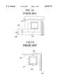
- FIG. 1Ashows such an example wherein a plurality of design standards are present at one portion of the mask pattern data. This example will be described by means of the regulation value of the spacing of wiring data 201 around the bonding pad.
- FIG. 1Bshows that wiring data 201 are classified by a bonding pad portion 303 into a wiring line 301 of the pad portion and a wiring line 302 outside the pad portion.
- pad opening data 202is part of mask pattern data that constitutes the bonding pad.
- the bonding pad portion 303is constituted by forming the pad opening data 202 on the wiring data 201.
- the wiring data 201 inside the bonding pad portion 303is classified into the wiring line 301 of the pad portion, and the wiring data 201 outside the bonding pad portion 303 is classified into the wiring line 302 outside the pad portion, respectively.
- the spacing between the wiring line 301 of the pad portion and the wiring line 302 outside the pad portionusually has a regulation value R B 204.
- the spacinghas a regulation value R A 203.
- the regulation value R A 203is smaller than the regulation value R B 204. In other words, regulation value R A 203 ⁇ regulation value R B 204.
- the first conventional methodhas a region data preparation process 502, a data division process 504, a design rule check process 507, and a design rule check process 509, as shown in FIG. 2.
- the region data preparation process 502inputs mask pattern data 501 and outputs region data 503.
- the data division process 504inputs the mask pattern data 501 and the region data 503 and outputs division data 505.
- the design rule check process 507inputs and checks a design standard A 506 storing a design rule consisting of a regulation value R A 203 as the regulation value of the spacing between the wiring line 301 of the pad portion and the wiring line 302 outside the pad portion, and the division data 505.
- the design rule check process 507outputs the check result to a design rule check result 510.
- the design rule check process 509inputs and checks a design standard B 508 storing a design rule consisting of a regulation value R B 204 as another regulation value of the spacing between the wiring line 301 of the pad portion and the wiring line 302 outside the pad portion, and the division data 505.
- the design rule check process 509outputs the check result to the design rule check result 510.
- FIG. 3shows an example of the mask pattern data stored in the mask pattern data 501.
- the spacing between the wiring data 201 inside the bonding pad portion 303 and the wiring data 201 outside the bonding pad portion 303includes a design value D A 601 and a design value D B 602.
- the design value D A 601is smaller than the regulation value R A 203 mentioned in the design standard example (design value D A 601 ⁇ regulation value R A 203).
- the design value D B 602is larger than the regulation value R A 203 and smaller than the regulation value R B 204 (regulation value R A 203 ⁇ design value D B 602 ⁇ regulation value R B 204).
- the pad opening data 202 used for constituting the bonding padis input from the mask pattern data 501 to the region data preparation process 502.
- a thickening process 701 for the pad opening data 202is performed by using a graphic operation process to prepare a pad region 702, and the pad region 702 is output to the region data 503.
- the wiring line 301 and wiring line 302are output to the division data 505.
- the wiring line 301 of the pad portionis prepared by obtaining, by using a graphic operation process, the OR of the region data 503 and wiring data 201.
- the wiring line 302 outside the pad portionis prepared by obtaining, by using a graphic operation process, the exclusive OR of the wiring data 201 and region data 503.
- the wiring data 201has been input to the data division process 504 from the mask pattern data 501.
- the pad region 702has been input to the data division process 504 from the region data 503.
- the design rule check process 507will be described by means of the case of a design rule consisting of the regulation value R A 203 stored in the design standard A 506 as the regulation value of the spacing between the wiring line 301 of the pad portion and the wiring line 302 outside the pad portion, the wiring line 301 of the pad portion and the wiring line 302 outside the pad portion which are stored in the division data 505.
- side data(a side A 801 and a side B 802) of a portion where the spacing between the wiring line 301 of the pad portion and the wiring line 302 outside the pad portion becomes smaller than the regulation value R A 203 is obtained.
- Polygon data obtained by connecting the vertices of the pair of side A 801 and side B 802is output to the design rule check result 510 as a design rule check error (an error A 901).
- design rule check process 509a process similar to the design rule check process 507 described above is performed except for the design standard B 508 that stores a design rule consisting of a regulation value R B 204 as another regulation value of the spacing between the wiring line 301 of the pad portion and the wiring line 302 outside the pad portion.
- the design standard B 508that stores a design rule consisting of a regulation value R B 204 as another regulation value of the spacing between the wiring line 301 of the pad portion and the wiring line 302 outside the pad portion.
- side datathe side A 801 and side B 802, a side C 803, and a side D 804 of portions where the spacing between the wiring line 301 of the pad portion and the wiring line 302 outside the pad portion becomes smaller than the regulation value regulation value R B 204 are obtained.
- Polygon data obtained by connecting the vertices of the pair of side A 801 and side B 802 and the pair of side C 803 and side D 804is output to the design rule check result 510 as a design rule check error (an error B 902 and an error B 903).
- FIG. 6shows an example of a design rule error which is output to the design rule check result 510, as described above.
- the error A 901indicates a design rule error which is output in the design rule check process 507
- the error B 902 and error B 903indicate design rule errors that are output in the design rule check process 509.
- FIGS. 7A and 7Bdescribe the content of the design rule errors shown in FIG. 6, in which FIG. 7A shows a design rule error (the error A 901) defined by the regulation value R A 203 as the regulation value of the spacing between the wiring line 301 of the pad portion and the wiring line 302 outside the pad portion
- FIG. 7Bshows design rule errors (the error B 902 and error B 903) defined by the regulation value R B 204 as another regulation value of the spacing between the wiring line 301 of the pad portion and the wiring line 302 outside the wiring line 302.
- Determination as to whether the design rule check error output to the design rule check result 510 is a true error or a pseudo-erroris conventionally performed manually through comparison and reference of the design standard example described above, the mask pattern example shown in FIG. 4, and the design rule check result 510 (FIGS. 7A and 7B).
- the error A 901can be determined as a true error since the spacing between the side A 801 and side B 802 shown in FIG. 5 is the design value D A 601, which is smaller than the regulation value R A 203.
- the error B 903can be determined as a true error since the spacing between the side C 803 and side D 804 shown in FIG. 7 is the design value D B 602, which is smaller than the regulation value R B 204.
- the error B 902it should be dealt with as a true error since the spacing between the side A 801 and side B 802 shown in FIG. 7 is the design value D A 601, which is smaller than the regulation value R B 204. However, since the error B 902 recurs at the same portion (the side A 801 and side B 802) where the error A 901 which is determined as a true error occurred. Also, the error portion on the mask pattern can be specified by the error A 901 described above. Thus, the error B 902 need not be handled as a true error and is determined as a kind of pseudo-error.
- the second conventional methodhas a check operation control unit 1201 for receiving data from an input unit 1202, a design standard file 1204, and mask pattern data 1203, for receiving/outputting a process file 1205 and a pseudo-error registration file 1207, and for outputting a design rule check result 1206, as shown in FIG. 8.
- a check operation control unit 1201for receiving data from an input unit 1202, a design standard file 1204, and mask pattern data 1203, for receiving/outputting a process file 1205 and a pseudo-error registration file 1207, and for outputting a design rule check result 1206, as shown in FIG. 8.
- the second conventional methodwill be described under the following assumption, in the same manner as the first conventional method. Namely, assume that the mask pattern data 1203 stores the mask pattern data shown in FIG.
- the design standard file 1204stores a design rule consisting of a regulation value R A 203 and regulation value R B 204 as the regulation values of the spacing between the wiring line 301 of the pad portion and the wiring line 302 outside the pad portion which are described in the design standard example.
- a process similar to the design rule check method of the first conventional methodis performed by the check operation control unit 1201, and a design rule check error is output to the process file 1205.
- the pseudo-error registration file 1207is not specified. Therefore, the content of the process file 1205 is directly output to the design rule check result 1206.
- the design rule check error output to the design rule check result 1206is a true error or a pseudo-error is manually determined.
- a design rule check errorwhich is determined as a pseudo-error (for example, the error B 902 shown in FIGS. 6 and 7B)
- the content of this pseudo-erroris manually written and registered in the pseudo-error registration file 1207 by the input unit 1202. If a design rule error is determined as a true error (for example, the error A 901 shown in FIGS. 6 and 7A), the mask pattern data is corrected manually.
- the mask pattern data whose true error is corrected in the initial design rule checkis stored in the mask pattern data 1203.
- the pseudo-error registration file 1207 in which registration is performed in the initial design rule checkis specified.
- a process similar to the first conventional design rule check methodis performed by the check operation control unit 1201, and a design rule check error is output to the process file 1205. Since the pseudo-error registration file 1207 is specified, the check operation control unit 1201 outputs, to the design rule check result 1206, a design rule check error obtained by removing the content registered in the pseudo-error registration file 1207 from the process file 1205.
- the design rule check error output to the process file 1205 in the second design rule checkdoes not include a true error, but includes a pseudo-error identical to the pseudo-error registered in the pseudo-error registration file 1207 in the initial design rule check.
- a design rule check result 1206 free from a pseudo-error that occurred in the initial design rule checkcan be obtained.
- the third conventional methodhas a design rule check process 1503 for receiving mask pattern data 1501 and a design standard file 1502 and outputting a design rule check error to a work file 1504, and a pseudo-error determination process 1505 for receiving the mask pattern data 1501 and the work file 1504 and outputting a design rule check error to a design rule check result 1506, as shown in FIG. 9.
- a design rule check process 1503for receiving mask pattern data 1501 and a design standard file 1502 and outputting a design rule check error to a work file 1504
- a pseudo-error determination process 1505for receiving the mask pattern data 1501 and the work file 1504 and outputting a design rule check error to a design rule check result 1506, as shown in FIG. 9.
- the design standard file 1502stores a design rule consisting of a regulation value R A 203 and regulation value R B 204 as the regulation values of the spacing between the wiring line 301 of the pad portion and the wiring line 302 outside the pad portion which are described in the design standard example.
- the design rule check process 1503performs a process similar to the design rule check process 507 and design rule check process 509 described in the first conventional method for the wiring line 301 of the pad portion and the wiring line 302 outside the pad portion to obtain a design rule check error (e.g., the error A 901, the error B 902, and the error B 903 shown in FIG. 6), and outputs the obtained design rule check error to the work file 1504.
- the pseudo-error determination process 1505reads the design rule check error stored in the work file 1504 as graphic data, and checks whether or not this design rule check error overlaps the mask pattern data stored in the mask pattern data 1501 in accordance with a graphic operation process.
- a true error and a pseudo-errorare determined among the design rule check errors (e.g., the error A 901, the error B 902, and the error B 903 shown in FIG. 6) in accordance with whether or not this overlap is present. Only a true error is output to the design rule check result 1506, so that a design rule check result 1506 free from a pseudo-error can be obtained.
- the design rule check errorse.g., the error A 901, the error B 902, and the error B 903 shown in FIG. 6
- the first to third conventional methodshave problems as follows.
- a design rule check error which recurs at one portionis a true error or a kind of pseudo-error is manually determined.
- the time required for making manual discrimination between a true error and a pseudo-errorbecomes necessary for the number of design rule check errors that recur, and a determination error can occur due to a human factor.
- a pseudo-error occurring in the initial design rule checkis registered and is removed in the second design rule check. Occurrence of a pseudo-error cannot be prevented with one design rule check, and design rule checks are required at least twice.
- the wiring data 204 in which a true error has been corrected in the initial design rule check and in which a pseudo-error occurred in the initial design rule checkis corrected (1302) to provide wiring data 1301, and that the resultant mask pattern data is stored in the layout file or mask pattern data 1203 to perform the second design rule check.
- the pseudo-errore.g., the error B 902 shown in FIGS.
- a pseudo-erroris determined by checking whether a design rule check error and the mask pattern data 1501 overlap or not. For example, since the error A 901 and error B 902 shown in FIG. 6 occur at the same portion, they are dealt with equivalently in this determination. In the process which determines the error A 901 as a true error, the error B 902 which should be determined as a pseudo-error is also erroneously determined as a true error and is output to the design rule check result 1506, so that occurrence of pseudo-errors cannot be prevented. Whether a design rule check error which recurs at one portion is a true error or a kind of pseudo-error must be manually determined. The time required for making manual discrimination between a true error and a pseudo-error becomes necessary for the number of design rule check errors that recur, and a determination error can occur due to a human factor, in the same manner as in the conventional methods described above.
- the present inventionhas been made in view of the above situations of the conventional technique, and has as its object to provide a design rule check method that prevents occurrence of pseudo-errors and does not require manual error determination.
- design rule checkfor inspecting whether or not mask pattern data of a semiconductor integrated circuit is correctly designed in accordance with a design standard, a design rule check method wherein design rule check errors occurring in the design rule check are discriminated between a first error and a second error and are output in accordance with whether or not the design rule check errors overlap.
- a methodhaving an overlap determination step of checking whether or not input design rule check error A and design rule check error B overlap, determining the design rule check error B not overlapping the design rule check error A as the first error, determining the design rule check error B overlapping the design rule check error A as the second error, and determining the design rule check error A as the first error, wherein the first error is output to a design rule check result.
- a methodhaving an overlap determination step of checking whether or not input design rule check error A and design rule check error B overlap, determining the design rule check error A not overlapping the design rule check error B as the first error, determining the design rule check error A overlapping the design rule check error B as the second error, and determining the design rule check error B as the first error.
- the design rule check error A and the design rule check error Bare not output to the design rule check result.
- the characteristic feature of the design rule check method of the present inventionresides in that design rule check errors occurring in the design rule check are discriminated between the first error as a signal error and the second error as a pseudo-error in accordance with whether they overlap or not, and the determined errors are output.
- occurrence of pseudo-errorscan be prevented by performing a design rule check once. Since occurrence of pseudo-errors is prevented, not only the time required for making manual determination between a true error and a pseudo-error becomes unnecessary, but also a determination error due to a human factor does not occur.
- FIG. 1Ashows regulation values of the spacing between wiring data around a bonding pad as a design standard example in the conventional technique
- FIG. 1Bshows that the wiring data are classified into a wiring line of the pad portion and a wiring line outside the pad portion;
- FIG. 2is a block diagram for explaining the first conventional method
- FIG. 3is a view showing an example of mask pattern data to be examined in a design rule check
- FIG. 4is a view for explaining a region data preparation process
- FIG. 5is a view for explaining a design rule check process
- FIG. 6is a view for explaining a design rule check error
- FIGS. 7A and 7Bare views for explaining the content of the design rule check error shown in FIG. 6;
- FIG. 8is a block diagram for explaining the second conventional method
- FIG. 9is a block diagram for explaining the third conventional method.
- FIG. 10is a view for explaining master pattern data obtained by correcting the wiring data of the second conventional method shown in FIG. 8;
- FIG. 11is a view showing a design rule check error which forms a pseudo-error in the second conventional method shown in FIG. 8;
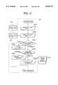
- FIG. 12is a block diagram showing the process of the design rule check method according to an embodiment of the present invention by way of its steps.
- FIG. 13is a flow chart showing the processing sequence of the error determination process of the embodiment shown in FIG. 12.
- FIG. 12is a block diagram showing the process according to an embodiment of the present invention by means of its steps.
- the present inventionis applied to a design rule check of mask pattern data that concerns a wiring line of the pad portion and a wiring line outside the pad portion, in the same manner as in the conventional technique described above.
- mask pattern data 101stores the mask pattern data shown in FIG. 4, in the same manner as in the conventional technique described above.
- Design standard A 102stores a design rule consisting of a regulation value R A 203 as the spacing between the wiring line 301 of the pad portion and the wiring line 302 outside the pad portion which are described in the design standard example.
- design standard B 105stores a design rule consisting of a regulation value R B 204 as the spacing between the wiring line 301 of the pad portion and the wiring line 302 outside the pad portion which are described in the design standard example, where a design rule check error that can be regarded as a pseudo-error in the prior art occurs.
- a region data preparation process 502for receiving the mask pattern data 101 and outputting region data 503, a data division process 504 for receiving the mask pattern data 101 and region data 503 and outputting division data 505, a design rule check process 103 for receiving the design standard A 102 storing the design rule consisting of the first regulation value R A 204 and the division data 505, and a design rule check process 106 for receiving the design standard B 105 storing the design rule consisting of the second regulation value R A 203 and division data 505.
- a design rule check error defined by the first regulation value R A 203 output in the design rule check process 103(e.g., the error A 901 shown in FIGS. 6 and 7A) is output to a work file A 104 as an error A
- a design rule check error defined by the second regulation value R B 204 output in the design rule check process 106(e.g., the error B 902 and error B 903 shown in FIGS. 6 and 7B) is output to a work file B 107 as an error B.
- FIG. 13is a flow chart showing the processing sequence of the error determination process 108.
- the error Ais input from the work file A 104.
- graphic data input 2 step S102the error B is input from the work file B 107. If neither the error A or B exists in data presence/absence step S103, it is determined that data does not exist, and the flow advances to the post-process via data non-output step S104. No design rule check error is output to a design rule check result 109.
- the error Ae.g., the error A 901 shown in FIGS. 6 and 7A
- the error Be.g., the error B 902 shown in FIGS. 6 and 7A
- the error Bis regarded as a second error (pseudo-error), and is not output to the design rule check result 109.
- the error Be.g., the error B 903 shown in FIGS.
- Tables 1 and 2show examples of the structure of a graphic data storage memory used in steps S101 to S103, and steps S105 to S107 of the error determination process 108.
- the graphic data storage memoryhas a column structure consisting of a data presence/absence flag, coordinate data, and a first error flag, and each column consists of rows of a count equal to the count of graphic data plus one row, thus constituting a row structure.
- the graphic data storage memory(a. memory A and b. memory B) shown in Tables 1 and 2 has a column structure as follows.
- a "1" data presence/absence flagindicates a case wherein graphic data is present and a "0" data presence/absence flag a case wherein the graphic data storage memory is ended or no data is present.
- the coordinate datathe coordinate values of all the vertices of the graphic data are shown inside the parentheses () with separation ":” in accordance with the order with which the sides of the graphic data are connected, while the X and Y coordinates of the coordinate values of the vertices are separated with ",”.
- a "1" first error flagindicates a case wherein the graphic data is the first error and a "0" first error flag a case wherein the graphic data is not the first error.
- the a. memory Ashows a state wherein the error A stored in the work file A 104 is input in graphic data input 1 step S101 and arranged on the graphic data storage memory (e.g., the error A 901 shown in FIGS. 6 and 7A is on the first row), and the b. memory B shows a state wherein the error B stored in the work file B 107 is input in graphic data input 2 step S102 and arranged on the graphic data storage memory (e.g., the error B 902 and error B 903 shown in FIGS. 6 and 7B are respectively on the first and second rows).
- the first error flagis set to "1"
- the data presence/absence flagis set to "0" in order to indicate the end of the graphic data storage memory.
- step S103absence of data is determined in accordance with whether or not the data presence/absence flag of the first row is "0" in each of the a. memory A and b. memory B.
- overlap determination step S105a set of coordinate data (e.g., the coordinate data of the first row of the a. memory A and the coordinate data of the first row of the b. memory B) are read from the a. memory A and b. memory B. If the coordinate values of all the vertices of the coordinate data of the a. memory A are located within a region indicated by the coordinate values of the respective vertices of the coordinate data of the b.
- graphic data output 1 step S106 and graphic data output 2 step S107coordinate data corresponding to a row where the first error flag and the data presence/absence flag of the graphic data storage memory are respectively "1" and "1" is output to the design rule check result 109 as graphic data.
- an overlapis determined when the coordinate values of all the vertices in the coordinate data of the a. memory A are located within the region indicated by the coordinate values of the respective vertices of the coordinate data of the b. memory B.
- an overlapmay be determined.
- an overlapis determined when at least one coordinate value of a vertex of the coordinate data of the a. memory A is located within the region indicated by the coordinate values of the respective vertices of the coordinate data of the b. memory B. Then, the same effect as that described above can be obtained.
- the present inventionis not limited to the embodiment described above, but can be constituted as follows.
- the error determination process 108has data presence/absence step S103.
- data presence/absence step S103 and data non-output step S104are omitted, the same effect as that described above can be obtained.
- pad opening datais used in order to obtain the wiring data of the pad portion. If the wiring data of the pad portion can be obtained by using another mask pattern data, the same process as that of the present invention may be performed by using another mask pattern to obtain the same effect as described above.
- a design rule check on the spacing of the wiring datais described in detail.
- the present inventionis not limited to a design rule check on the width of the wiring data or on wiring data of the bonding pad portion. Even in a design rule check of another mask pattern data, if a plurality of design standards exist at one portion on the mask pattern, the same process as that described above may be performed to obtain the same effect.
- overlap determination step S105when an overlap exists, the error A is regarded as a first error.
- graphic data output 1 step S106may be altered such that the error B is regarded as a first error and that the error A is regarded as a second error, thus obtaining the same effect.
- a design rule check processis performed.
- a data division processis not required (e.g., if the wiring line of the pad portion and the wiring line outside the pad portion are constituted as different data on the mask pattern data)
- the region data preparation process 502 and data division process 504may be omitted and the same process may be performed by using the mask pattern data 101 as inputs to the design rule check processes 103 and 106, thus obtaining the same effect as described above.
Landscapes
- Engineering & Computer Science (AREA)
- Computer Hardware Design (AREA)
- Physics & Mathematics (AREA)
- Theoretical Computer Science (AREA)
- Evolutionary Computation (AREA)
- Geometry (AREA)
- General Engineering & Computer Science (AREA)
- General Physics & Mathematics (AREA)
- Design And Manufacture Of Integrated Circuits (AREA)
- Testing Or Measuring Of Semiconductors Or The Like (AREA)
Abstract
Description
TABLE 1 ______________________________________ a.Memory A 1 3 Data Presence/First Absence 2 Error Flag Coordinate Data Flag ______________________________________ 1 1 (Xa11, Ya11:Xa12, Ya12: 1 Xa13, Ya13:Xa14, Ya14) 2 0 -- -- ______________________________________
TABLE 2 ______________________________________ b.Memory B 1 3 Data Presence/First Absence 2 Error Flag Coordinate Data Flag ______________________________________ 1 1 (Xb11, Yb11:Xb12, Yb12: 1 Xb13, Yb13:Xb14, Yb14) 2 1 (Xb21, Yb21:Xb22, Yb22: 1 Xb23, Yb23:Xb24, Yb24) 3 0 -- -- ______________________________________
Claims (5)
Applications Claiming Priority (2)
| Application Number | Priority Date | Filing Date | Title |
|---|---|---|---|
| JP8251152AJP2914316B2 (en) | 1996-09-24 | 1996-09-24 | How to check design rules |
| JP8-251152 | 1996-09-24 |
Publications (1)
| Publication Number | Publication Date |
|---|---|
| US6078737Atrue US6078737A (en) | 2000-06-20 |
Family
ID=17218456
Family Applications (1)
| Application Number | Title | Priority Date | Filing Date |
|---|---|---|---|
| US08/932,960Expired - Fee RelatedUS6078737A (en) | 1996-09-24 | 1997-09-18 | Design rule check method |
Country Status (2)
| Country | Link |
|---|---|
| US (1) | US6078737A (en) |
| JP (1) | JP2914316B2 (en) |
Cited By (25)
| Publication number | Priority date | Publication date | Assignee | Title |
|---|---|---|---|---|
| US6341366B1 (en)* | 1999-01-15 | 2002-01-22 | Spring Soft Inc. | Rule-driven method and system for editing physical integrated circuit layouts |
| US6397373B1 (en)* | 1999-07-12 | 2002-05-28 | Taiwan Semiconductor Manufacturing Company | Efficient design rule check (DRC) review system |
| US20020138813A1 (en)* | 2001-03-20 | 2002-09-26 | Cheehoe Teh | System & method for performing design rule check |
| US6618840B2 (en)* | 2001-02-12 | 2003-09-09 | Hewlett-Packard Development Company, L.P. | Method and system for analyzing a VLSI circuit design |
| US20030229862A1 (en)* | 2002-06-10 | 2003-12-11 | Sun Microsystems, Inc. | Patching technique for correction of minimum area and jog design rule violations |
| US20040019862A1 (en)* | 2002-07-23 | 2004-01-29 | Sun Microsystems, Inc. | Structure and method for separating geometries in a design layout into multi-wide object classes |
| US20040025098A1 (en)* | 2002-05-29 | 2004-02-05 | Dirk Meyer | Method for classifying errors in the layout of a semiconductor circuit |
| US20040039718A1 (en)* | 2002-08-22 | 2004-02-26 | International Business Machines Corps. | Loop detection in rule-based expert systems |
| US6708323B2 (en)* | 2000-08-09 | 2004-03-16 | Fujitsu Limited | Method and apparatus for verifying mask pattern data according to given rules |
| US20040064795A1 (en)* | 2002-09-30 | 2004-04-01 | Sun Microsystems, Inc. | Via enclosure rule check in a multi-wide object class design layout |
| US20040063228A1 (en)* | 2002-09-30 | 2004-04-01 | Sun Microsystems, Inc. | Redundant via rule check in a multi-wide object class design layout |
| US20040064797A1 (en)* | 2002-09-30 | 2004-04-01 | Sun Microsystems, Inc. | Pure fill via area extraction in a multi-wide object class design layout |
| US6735749B2 (en) | 2002-03-21 | 2004-05-11 | Sun Microsystems, Inc. | (Design rule check)/(electrical rule check) algorithms using a system resolution |
| US6769099B2 (en) | 2002-04-12 | 2004-07-27 | Sun Microsystems, Inc. | Method to simplify and speed up design rule/electrical rule checks |
| US6769103B2 (en) | 2002-07-19 | 2004-07-27 | Micron Technology, Inc. | Line width check in layout database |
| US20040255258A1 (en)* | 2003-06-13 | 2004-12-16 | Sun Microsystems, Inc. | Method, apparatus, and computer program product for generation of a via array within a fill area of a design layout |
| US20050050511A1 (en)* | 2003-08-25 | 2005-03-03 | Infineon Technologies North America Corp. | System and method of correcting mask rule violations after optical proximity correction |
| US6895568B2 (en) | 2002-09-30 | 2005-05-17 | Sun Microsystems, Inc. | Correction of spacing violations between pure fill via areas in a multi-wide object class design layout |
| US20060090144A1 (en)* | 2004-10-27 | 2006-04-27 | Lsi Logic Corporation | Method of automating place and route corrections for an integrated circuit design from physical design validation |
| US7096447B1 (en) | 2003-10-15 | 2006-08-22 | Sun Microsystems, Inc. | Method and apparatus for efficiently locating and automatically correcting certain violations in a complex existing circuit layout |
| US20070162882A1 (en)* | 2005-12-14 | 2007-07-12 | Kabushiki Kaisha Toshiba | Design support system of semiconductor integrated circuit, method of designing semiconductor integrated circuit, design support program of semiconductor integrated circuit and method of manufacturing semiconductor integrated circuit |
| US20080184183A1 (en)* | 2007-01-26 | 2008-07-31 | Sachiko Kobayashi | Pattern forming method and pattern verifying method |
| US20110055778A1 (en)* | 2009-08-28 | 2011-03-03 | Taiwan Semiconductor Manufacturing Company, Ltd. | Automatic Application-Rule Checker |
| WO2013019791A1 (en)* | 2011-08-02 | 2013-02-07 | Anderson Tom H C | Natural language test analytics |
| US8707231B2 (en) | 2012-07-31 | 2014-04-22 | Freescale Semiconductor, Inc. | Method and system for derived layer checking for semiconductor device design |
Families Citing this family (1)
| Publication number | Priority date | Publication date | Assignee | Title |
|---|---|---|---|---|
| JP5740882B2 (en)* | 2010-09-16 | 2015-07-01 | 株式会社リコー | Layout data error determination method, layout data error determination device, layout data creation device, and layout data error determination program |
Citations (3)
| Publication number | Priority date | Publication date | Assignee | Title |
|---|---|---|---|---|
| US5225993A (en)* | 1990-02-17 | 1993-07-06 | Mitsubishi Denki Kabushiki Kaisha | Design rule test apparatus for testing if mask pattern satisfies design rule and operation method therefor |
| US5620916A (en)* | 1993-04-27 | 1997-04-15 | Intel Corporation | Method for improving via/contact coverage in an integrated circuit |
| US5706295A (en)* | 1995-07-28 | 1998-01-06 | Nec Corporation | Method of checking design rules for semiconductor integrated circuit |
- 1996
- 1996-09-24JPJP8251152Apatent/JP2914316B2/ennot_activeExpired - Fee Related
- 1997
- 1997-09-18USUS08/932,960patent/US6078737A/ennot_activeExpired - Fee Related
Patent Citations (3)
| Publication number | Priority date | Publication date | Assignee | Title |
|---|---|---|---|---|
| US5225993A (en)* | 1990-02-17 | 1993-07-06 | Mitsubishi Denki Kabushiki Kaisha | Design rule test apparatus for testing if mask pattern satisfies design rule and operation method therefor |
| US5620916A (en)* | 1993-04-27 | 1997-04-15 | Intel Corporation | Method for improving via/contact coverage in an integrated circuit |
| US5706295A (en)* | 1995-07-28 | 1998-01-06 | Nec Corporation | Method of checking design rules for semiconductor integrated circuit |
Non-Patent Citations (8)
| Title |
|---|
| Bhat et al., "Special Purpose Architecture for Accelerating Bitmap DRC" 26th ACM/EEE Design Automation Conference pp. 674-677 (Jan. 1989). |
| Bhat et al., Special Purpose Architecture for Accelerating Bitmap DRC 26th ACM/EEE Design Automation Conference pp. 674 677 (Jan. 1989).* |
| Crawford et al., "Computer verification fo Large Scale Integrated Circuit Masks" IEEE pp. 132-135 (1978). |
| Crawford et al., Computer verification fo Large Scale Integrated Circuit Masks IEEE pp. 132 135 (1978).* |
| Hedenstierna et al. ( The halo algorithm an algorithm for hierarchical design of rule checking of VLSI circuits , IEEE Transactions on Computer Aided Design of Integrated Circuits and Systems, vol. 12, No. 2, Feb. 1993, pp. 265 272.* |
| Hedenstierna et al. ("The halo algorithm--an algorithm for hierarchical design of rule checking of VLSI circuits", IEEE Transactions on Computer-Aided Design of Integrated Circuits and Systems, vol. 12, No. 2, Feb. 1993, pp. 265-272. |
| Modarres et al., "A Formal Approach to Desing-Rule Checking" IEEE Transactions on Computer-Aided Design pp. 561-573 (1987), vol. CAD-6, No. 4, Jul. 1987. |
| Modarres et al., A Formal Approach to Desing Rule Checking IEEE Transactions on Computer Aided Design pp. 561 573 (1987), vol. CAD 6, No. 4, Jul. 1987.* |
Cited By (57)
| Publication number | Priority date | Publication date | Assignee | Title |
|---|---|---|---|---|
| US6341366B1 (en)* | 1999-01-15 | 2002-01-22 | Spring Soft Inc. | Rule-driven method and system for editing physical integrated circuit layouts |
| US6397373B1 (en)* | 1999-07-12 | 2002-05-28 | Taiwan Semiconductor Manufacturing Company | Efficient design rule check (DRC) review system |
| US6708323B2 (en)* | 2000-08-09 | 2004-03-16 | Fujitsu Limited | Method and apparatus for verifying mask pattern data according to given rules |
| US6618840B2 (en)* | 2001-02-12 | 2003-09-09 | Hewlett-Packard Development Company, L.P. | Method and system for analyzing a VLSI circuit design |
| US20020138813A1 (en)* | 2001-03-20 | 2002-09-26 | Cheehoe Teh | System & method for performing design rule check |
| US7552408B2 (en) | 2001-03-20 | 2009-06-23 | United Microelectronics Corporation | Method for performing design rule check on mask pattern data for an integrated circuit |
| US6816997B2 (en) | 2001-03-20 | 2004-11-09 | Cheehoe Teh | System and method for performing design rule check |
| US20050086619A1 (en)* | 2001-03-20 | 2005-04-21 | Cheehoe Teh | System & method for performing design rule check |
| US6735749B2 (en) | 2002-03-21 | 2004-05-11 | Sun Microsystems, Inc. | (Design rule check)/(electrical rule check) algorithms using a system resolution |
| US6769099B2 (en) | 2002-04-12 | 2004-07-27 | Sun Microsystems, Inc. | Method to simplify and speed up design rule/electrical rule checks |
| US20040025098A1 (en)* | 2002-05-29 | 2004-02-05 | Dirk Meyer | Method for classifying errors in the layout of a semiconductor circuit |
| US7207016B2 (en)* | 2002-05-29 | 2007-04-17 | Infineon Technologies Ag | Method for classifying errors in the layout of a semiconductor circuit |
| US20070157142A1 (en)* | 2002-05-29 | 2007-07-05 | Infineon Technologies Ag | Method for classifying errors in the layout of a semiconductor circuit |
| US7716613B2 (en) | 2002-05-29 | 2010-05-11 | Qimonda Ag | Method for classifying errors in the layout of a semiconductor circuit |
| US6892368B2 (en) | 2002-06-10 | 2005-05-10 | Sun Microsystems, Inc. | Patching technique for correction of minimum area and jog design rule violations |
| US20030229862A1 (en)* | 2002-06-10 | 2003-12-11 | Sun Microsystems, Inc. | Patching technique for correction of minimum area and jog design rule violations |
| US6769103B2 (en) | 2002-07-19 | 2004-07-27 | Micron Technology, Inc. | Line width check in layout database |
| US20040163063A1 (en)* | 2002-07-19 | 2004-08-19 | Micron Technology, Inc. | Line width check in layout database |
| US20040163060A1 (en)* | 2002-07-19 | 2004-08-19 | Micron Technology, Inc. | Line width error check |
| US20040168139A1 (en)* | 2002-07-19 | 2004-08-26 | Micron Technology, Inc. | Identifying line width errors in integrated circuit designs |
| US20040163064A1 (en)* | 2002-07-19 | 2004-08-19 | Micron Technology, Inc. | Line width check in layout database |
| US6944839B2 (en) | 2002-07-19 | 2005-09-13 | Micron Technology, Inc. | Checking layout accuracy in integrated circuit designs |
| US7428714B2 (en) | 2002-07-19 | 2008-09-23 | Micron Technology, Inc. | Line width error check |
| US7120889B2 (en) | 2002-07-19 | 2006-10-10 | Micron Technology, Inc. | Integrated circuit schematics and layouts |
| US7107554B2 (en) | 2002-07-19 | 2006-09-12 | Micron Technology, Inc. | Line width check in layout database |
| US20040163061A1 (en)* | 2002-07-19 | 2004-08-19 | Micron Technology, Inc. | Design rule checking integrated circuits |
| US7055115B2 (en) | 2002-07-19 | 2006-05-30 | Micron Technology, Inc. | Line width check in layout database |
| US7032199B2 (en) | 2002-07-19 | 2006-04-18 | Micron Technology, Inc. | Design rule checking integrated circuits |
| US7024643B2 (en) | 2002-07-19 | 2006-04-04 | Micron Technology, Inc. | Identifying line width errors in integrated circuit designs |
| US6871332B2 (en) | 2002-07-23 | 2005-03-22 | Sun Microsystems, Inc. | Structure and method for separating geometries in a design layout into multi-wide object classes |
| US20040019862A1 (en)* | 2002-07-23 | 2004-01-29 | Sun Microsystems, Inc. | Structure and method for separating geometries in a design layout into multi-wide object classes |
| US20040039718A1 (en)* | 2002-08-22 | 2004-02-26 | International Business Machines Corps. | Loop detection in rule-based expert systems |
| US6952690B2 (en) | 2002-08-22 | 2005-10-04 | International Business Machines Corporation | Loop detection in rule-based expert systems |
| US6883149B2 (en) | 2002-09-30 | 2005-04-19 | Sun Microsystems, Inc. | Via enclosure rule check in a multi-wide object class design layout |
| US20040064795A1 (en)* | 2002-09-30 | 2004-04-01 | Sun Microsystems, Inc. | Via enclosure rule check in a multi-wide object class design layout |
| US6804808B2 (en) | 2002-09-30 | 2004-10-12 | Sun Microsystems, Inc. | Redundant via rule check in a multi-wide object class design layout |
| US6895568B2 (en) | 2002-09-30 | 2005-05-17 | Sun Microsystems, Inc. | Correction of spacing violations between pure fill via areas in a multi-wide object class design layout |
| US6832360B2 (en) | 2002-09-30 | 2004-12-14 | Sun Microsystems, Inc. | Pure fill via area extraction in a multi-wide object class design layout |
| US20040064797A1 (en)* | 2002-09-30 | 2004-04-01 | Sun Microsystems, Inc. | Pure fill via area extraction in a multi-wide object class design layout |
| US20040063228A1 (en)* | 2002-09-30 | 2004-04-01 | Sun Microsystems, Inc. | Redundant via rule check in a multi-wide object class design layout |
| US7007258B2 (en) | 2003-06-13 | 2006-02-28 | Sun Microsystems, Inc. | Method, apparatus, and computer program product for generation of a via array within a fill area of a design layout |
| US20040255258A1 (en)* | 2003-06-13 | 2004-12-16 | Sun Microsystems, Inc. | Method, apparatus, and computer program product for generation of a via array within a fill area of a design layout |
| US20050050511A1 (en)* | 2003-08-25 | 2005-03-03 | Infineon Technologies North America Corp. | System and method of correcting mask rule violations after optical proximity correction |
| US7062748B2 (en)* | 2003-08-25 | 2006-06-13 | Infineon Technologies Ag | System and method of correcting mask rule violations after optical proximity correction |
| US7096447B1 (en) | 2003-10-15 | 2006-08-22 | Sun Microsystems, Inc. | Method and apparatus for efficiently locating and automatically correcting certain violations in a complex existing circuit layout |
| US20060090144A1 (en)* | 2004-10-27 | 2006-04-27 | Lsi Logic Corporation | Method of automating place and route corrections for an integrated circuit design from physical design validation |
| US20070162882A1 (en)* | 2005-12-14 | 2007-07-12 | Kabushiki Kaisha Toshiba | Design support system of semiconductor integrated circuit, method of designing semiconductor integrated circuit, design support program of semiconductor integrated circuit and method of manufacturing semiconductor integrated circuit |
| US8171445B2 (en) | 2005-12-14 | 2012-05-01 | Kabushiki Kaisha Toshiba | Replacing single-cut via into multi-cut via in semiconductor integrated circuit design |
| US7634751B2 (en)* | 2005-12-14 | 2009-12-15 | Kabushiki Kaisha Toshiba | Replacing single-cut via into multi-cut via in semiconductor integrated circuit design |
| US8386970B2 (en) | 2005-12-14 | 2013-02-26 | Kabushiki Kaisha Toshiba | Replacing single-cut via into multi-cut via in semiconductor integrated circuit design |
| US20080184183A1 (en)* | 2007-01-26 | 2008-07-31 | Sachiko Kobayashi | Pattern forming method and pattern verifying method |
| US8261217B2 (en)* | 2007-01-26 | 2012-09-04 | Kabushiki Kaisha Toshiba | Pattern forming method and pattern verifying method |
| US20110055778A1 (en)* | 2009-08-28 | 2011-03-03 | Taiwan Semiconductor Manufacturing Company, Ltd. | Automatic Application-Rule Checker |
| US8943453B2 (en) | 2009-08-28 | 2015-01-27 | Taiwan Semiconductor Manufacturing Company, Ltd. | Automatic application-rule checker |
| WO2013019791A1 (en)* | 2011-08-02 | 2013-02-07 | Anderson Tom H C | Natural language test analytics |
| US8473498B2 (en) | 2011-08-02 | 2013-06-25 | Tom H. C. Anderson | Natural language text analytics |
| US8707231B2 (en) | 2012-07-31 | 2014-04-22 | Freescale Semiconductor, Inc. | Method and system for derived layer checking for semiconductor device design |
Also Published As
| Publication number | Publication date |
|---|---|
| JP2914316B2 (en) | 1999-06-28 |
| JPH1098107A (en) | 1998-04-14 |
Similar Documents
| Publication | Publication Date | Title |
|---|---|---|
| US6078737A (en) | Design rule check method | |
| US5838581A (en) | Layout system for logic circuit | |
| US5706295A (en) | Method of checking design rules for semiconductor integrated circuit | |
| EP0380720A1 (en) | Image processing method | |
| US5261033A (en) | Method of and apparatus for converting line graphic into graphic having curve | |
| US4591905A (en) | Color image data processing device for correcting red ghosts of black images | |
| US6643826B2 (en) | Semiconductor circuit connection data base and method of designing semiconductor circuit using the data base | |
| JPH04225149A (en) | Apparatus and method for three-state database for automatic optical inspection system | |
| US6550051B1 (en) | Lithographic data verification method and photo mask manufacturing method | |
| US5325476A (en) | Method of converting area data into path data | |
| JP2536398B2 (en) | How to fix printed wiring pattern corner | |
| US3698072A (en) | Validation technique for integrated circuit manufacture | |
| US7310791B2 (en) | Method for correcting layout errors | |
| JP2531084B2 (en) | Parts gap check device | |
| JPS6186639A (en) | pattern inspection equipment | |
| JPH0520433A (en) | Inspection device for printed wiring board | |
| US5889531A (en) | Graphic processing apparatus | |
| JP3413733B2 (en) | Method for checking interference between shapes | |
| KR100234982B1 (en) | Automatic execution-order decision method for function blocks in a logic diagram | |
| JPS60107832A (en) | Electron beam drawing method | |
| JPH07243984A (en) | Image pattern inspection device | |
| JP2957708B2 (en) | Method and apparatus for inspecting output dots of semiconductor device | |
| JP3063925B2 (en) | Image pattern matching device | |
| JP2876594B1 (en) | Failure detection system in interconnection | |
| JPH0361839A (en) | Inspecting apparatus for printed wiring board |
Legal Events
| Date | Code | Title | Description |
|---|---|---|---|
| AS | Assignment | Owner name:NEC CORPORATION, JAPAN Free format text:ASSIGNMENT OF ASSIGNORS INTEREST;ASSIGNOR:SUZUKI, KYOU;REEL/FRAME:008807/0429 Effective date:19970911 | |
| FEPP | Fee payment procedure | Free format text:PAYOR NUMBER ASSIGNED (ORIGINAL EVENT CODE: ASPN); ENTITY STATUS OF PATENT OWNER: LARGE ENTITY | |
| AS | Assignment | Owner name:NEC COMPOUND SEMICONDUCTOR DEVICES, LTD., JAPAN Free format text:ASSIGNMENT OF ASSIGNORS INTEREST;ASSIGNOR:NEC CORPORATION;REEL/FRAME:013392/0729 Effective date:20020919 | |
| FPAY | Fee payment | Year of fee payment:4 | |
| AS | Assignment | Owner name:NEC ELECTRONICS CORPORATION, JAPAN Free format text:ASSIGNMENT OF ASSIGNORS INTEREST;ASSIGNOR:NEC COMPOUND SEMICONDUCTOR DEVICES, LTD.;REEL/FRAME:017422/0528 Effective date:20060315 | |
| FPAY | Fee payment | Year of fee payment:8 | |
| REMI | Maintenance fee reminder mailed | ||
| LAPS | Lapse for failure to pay maintenance fees | ||
| STCH | Information on status: patent discontinuation | Free format text:PATENT EXPIRED DUE TO NONPAYMENT OF MAINTENANCE FEES UNDER 37 CFR 1.362 | |
| FP | Lapsed due to failure to pay maintenance fee | Effective date:20120620 |