US6078216A - Aliased wide band performance monitor for adjusting predistortion and vector modulator control parameters of RF amplifier - Google Patents
Aliased wide band performance monitor for adjusting predistortion and vector modulator control parameters of RF amplifierDownload PDFInfo
- Publication number
- US6078216A US6078216AUS09/053,529US5352998AUS6078216AUS 6078216 AUS6078216 AUS 6078216AUS 5352998 AUS5352998 AUS 5352998AUS 6078216 AUS6078216 AUS 6078216A
- Authority
- US
- United States
- Prior art keywords
- intermodulation distortion
- signal
- amplifier
- coupled
- output
- Prior art date
- Legal status (The legal status is an assumption and is not a legal conclusion. Google has not performed a legal analysis and makes no representation as to the accuracy of the status listed.)
- Expired - Lifetime
Links
- 238000012545processingMethods0.000claimsabstractdescription51
- 238000001228spectrumMethods0.000claimsabstractdescription29
- 230000003044adaptive effectEffects0.000claimsabstractdescription20
- 230000035945sensitivityEffects0.000claimsabstractdescription17
- 238000012544monitoring processMethods0.000claimsabstractdescription15
- 238000012937correctionMethods0.000claimsdescription22
- 238000000034methodMethods0.000claimsdescription17
- 239000002131composite materialSubstances0.000claimsdescription9
- 230000007246mechanismEffects0.000claimsdescription8
- 238000005259measurementMethods0.000claimsdescription7
- 238000005070samplingMethods0.000claimsdescription6
- 238000012546transferMethods0.000claimsdescription6
- 230000008569processEffects0.000claimsdescription5
- 238000011144upstream manufacturingMethods0.000claimsdescription3
- 238000009795derivationMethods0.000claims2
- 230000003595spectral effectEffects0.000abstractdescription8
- 238000000605extractionMethods0.000abstractdescription6
- 238000004891communicationMethods0.000description5
- 238000010168coupling processMethods0.000description5
- 238000005859coupling reactionMethods0.000description5
- 230000006978adaptationEffects0.000description4
- 230000001276controlling effectEffects0.000description4
- 230000008878couplingEffects0.000description4
- 238000002347injectionMethods0.000description3
- 239000007924injectionSubstances0.000description3
- 230000002238attenuated effectEffects0.000description2
- 238000010586diagramMethods0.000description2
- 238000003780insertionMethods0.000description2
- 230000037431insertionEffects0.000description2
- 238000012986modificationMethods0.000description2
- 230000004048modificationEffects0.000description2
- 238000010845search algorithmMethods0.000description2
- 230000003321amplificationEffects0.000description1
- 230000003466anti-cipated effectEffects0.000description1
- 238000013459approachMethods0.000description1
- 230000008901benefitEffects0.000description1
- 230000015556catabolic processEffects0.000description1
- 230000005574cross-species transmissionEffects0.000description1
- 238000006731degradation reactionMethods0.000description1
- 230000003111delayed effectEffects0.000description1
- 239000000284extractSubstances0.000description1
- 238000003199nucleic acid amplification methodMethods0.000description1
- 238000012805post-processingMethods0.000description1
- 238000007781pre-processingMethods0.000description1
- 230000001105regulatory effectEffects0.000description1
- 230000007480spreadingEffects0.000description1
- 230000000087stabilizing effectEffects0.000description1
Images

Classifications
- H—ELECTRICITY
- H03—ELECTRONIC CIRCUITRY
- H03F—AMPLIFIERS
- H03F1/00—Details of amplifiers with only discharge tubes, only semiconductor devices or only unspecified devices as amplifying elements
- H03F1/32—Modifications of amplifiers to reduce non-linear distortion
- H03F1/3223—Modifications of amplifiers to reduce non-linear distortion using feed-forward
- H03F1/3229—Modifications of amplifiers to reduce non-linear distortion using feed-forward using a loop for error extraction and another loop for error subtraction
Definitions
- the present inventionrelates in general to communication systems, and is particularly directed to a new and improved digital signal processor-resident performance monitor for an RF power amplifier.
- the performance monitoris operative to process aliased data representative of amplifier distortion so as to define and controllably update control parameter signals for controlling the operation of an adaptive predistortion unit and a vector modulator of a preamplification signal processing loop, and the vector modulator of a feed-forward error correction and reinjection loop, so as to minimize or maximally cancel intermodulation distortion products in the signal path through the amplifier.
- Communication service providersare subject to very strict bandwidth usage spectrum constraints, such as technically mandated specifications and regulations imposed by the Federal Communications Commission (FCC), which currently requires that sideband spillage, namely the amount of energy spillover outside a licensed band of interest, be sharply attenuated (e.g., on the order of 60 dB). While such limitations are adequate for traditional forms of modulation such as frequency modulation (FM), they are difficult to achieve using more contemporary, digitally based modulation formats, such as M-ary modulation.
- FCCFederal Communications Commission
- linear componentscan be implemented at a reasonable cost at relatively low bandwidths (baseband) used in telephone networks, linearizing such components, especially RF power amplifiers, becomes a very costly exercise.
- RF power amplifiersare inherently non-linear devices, and generate unwanted intermodulation distortion products (IMDs), which manifest themselves as spurious signals in the amplified RF output signal, separate and distinct from the RF input signal.
- IMDsintermodulation distortion products
- This intermodulation distortionis also referred to as spectral regrowth, or spreading of a compact spectrum into spectral regions that do not appear in the RF input signal.
- the distortion introduced by an RF amplifiercauses the phase and amplitude of its amplified output signal to depart from the respective phase and amplitude of the input signal, and may be considered as an incidental (and undesired) amplifier-sourced modulation of the input signal.
- a preprocessing correction loopThe purpose of a preprocessing correction loop is to modify the RF amplifier's input signal path.
- the control signalcauses the signal path adjustment mechanism to produce a signal control characteristic that has been predetermined to be equal and opposite to the distortion expected at the output of the RF amplifier.
- the mechanismmay be made adaptive by extracting the RF error signal component in the output of the RF amplifier and adjusting the control signal in accordance with the such extracted error behavior of the RF amplifier during real time operation, so as to effectively continuously reduce distortion in the amplifier's output.
- a post-processing, feed-forward correction loopserves to extract the amount of RF error (distortion) present in the RF amplifier's output signal, amplify that extracted distortion signal to the proper level, and then reinject the inverse of the amplified RF error signal back into a downstream output path of the RF amplifier, so that (ideally) the amplifier distortion is effectively canceled.
- the output of the RF amplifieris combined in an RF cancellation combiner with the RF input signal (which is used as a reference), in order that all carrier components (which give rise to the intermodulation distortion products) are effectively canceled, leaving only the RF error.
- an aliased digital signal processor-resident RF power amplifier performance monitoris operative to update control parameter signals in a manner that effectively minimizes or maximally cancels intermodulation distortion products in the signal path through the amplifier.
- the control parameter signalsare used to control the operation of each of an adaptive predistortion unit and a vector modulator of a preamplification signal processing loop, as well as the operation a vector modulator of a feed-forward error correction and reinjection loop.
- the adaptive predistortion unitis coupled to receive a set of weighting coefficients supplied by the digital signal processor, while the vector modulator has respective amplitude/gain and phase control inputs to which amplitude and phase adjustment signals (G 1 , ⁇ 1 ) are supplied by the processor.
- the RF input portis further coupled to an RF carrier cancellation combiner of the feed-forward error correction and reinjection loop.
- a portion of the amplified signal output of the RF amplifier(representative of the amplified original RF input signal and any intermodulation (spectral regrowth) distortion products (IMDs) introduced by the amplifier) is also coupled to the carrier cancellation combiner.
- the cancellation combinerserves to cancel all carrier components (which give rise to the intermodulation distortion products), leaving only the RF error.
- the RF error signal produced by the RF cancellation combineris coupled to a vector modulator of the feed-forward error correction and reinjection loop.
- the output of the vector modulatoris amplified in a feed-forward error amplifier, and then reinjected into the output path of the RF amplifier.
- the vector modulator of the feed-forward injection loophas respective amplitude and phase control inputs, to which respective amplitude and phase adjustment signals (G 2 , ⁇ 2 ) are supplied by the performance monitoring processor.
- the output of the RF carrier cancellation combiner(representative of the intermodulation distortion products in the output of the RF amplifier) and the composite signal in the reinjected output path of the RF amplifier are controllably coupled through a loop monitoring switch to a down-converting mixer, the output of which is coupled to wideband sub sampling analog-to-digital converter.
- the output of the analog-to-digital converteris less than the Nyquist criterion and therefore is ⁇ aliased ⁇ data.
- the digitized aliased datais buffered through a first-in, first-out (FIFO) serial buffer, so that it may be transferred at a data rate that is compatible with the processing speed of the processor.
- the sub sampled datais processed in accordance with a performance monitoring and control parameter updating processing routine which is operative to update the weighting coefficients to the predistortion compensation unit, and the two sets of amplitude and phase control signals for the two vector modulators.
- the processed dataproduces updated values that are converted to analog format by a digital-to-analog converter and applied to the predistortion unit and the vector modulators.
- the performance monitoring routineproduces respective products of a respective block of data samples and a window function WIN, such as a conventional Blackman-Harris window function.
- the samples S iare multiplied by successive components M i of a sensitivity mask function M, which represents a known carrier versus intermodulation distortion function associated with the operation of the RF amplifier.
- This IMD power datais processed in accordance with an error minimization operator through which the controlled parameters w, G and ⁇ are controllably adjusted.
- the error minimization operatormay comprise sequential, maximal descent, perturbational gradient search mechanism.
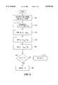
- the maskis reset to all ones. This allows all spectral components to be observed.
- the maximum value S max of the sequence of spectral power values S i as produced by the conjugate and multiply functionis identified.
- the value of S iis compared with the upper and lower limit values T U and T L . As long as S i falls between the upper and lower limits, M i is set at 1. Otherwise, M i is set to 0.
- the frequency at which the control parameters (w 1 - n , G 1 and ⁇ 1 ) of the preamplification signal processing loop, and the control parameters (G 2 and ⁇ 2 ) of the feed-forward error correction and reinjection loop are updatedis determined in accordance with the operation of the loop monitoring switch. Setting the initial values for and adjusting the sensitivity mask, as well as the control parameters for the loops is performed by controlling connectivity through the switch to couple downconverted data representative of the composite RF signal, subsequent to error signal reinjection in the RF amplifier's signal output path, to the processor. The rate at which connectivity through the switch is changed between loop-coupling input ports is determined by the intended rate of adaptation and monitored error variation.
- the switchIn order to establish the control parameters for the vector modulator of the preamplification signal processing loop, the switch is initially coupled to the input signal flow path. The signal spectrum is evaluated and a carrier (sensitivity) mask Mnew is defined. Next, an average mask value Mave is set equal to a previous mask value Mold*A+(1-A)*Mnew, where A is a constant less than 1. To maximize error extraction, the switch is then coupled to monitor the output of the RF carrier cancellation combiner. As data is collected, the spectrum is reevaluated. The spectrum data are multiplied by (1-Mi), so as to effectively leave only the carrier power in the resulting sum. The gain and phase control parameters (G 1 and ⁇ 1 ) for the vector modulator of the preamplification signal processing loop 20 are then adjusted so as to minimize carrier power, using a perturbational algorithm, such as a sequential, maximal descent, perturbational gradient search algorithm.
- a perturbational algorithmsuch as a sequential, maximal descent, perturbational gradient search algorithm.
- the switchis initially coupled to the amplified signal output path.
- the spectrumis evaluated and a carrier mask Mnew is defined.
- an average mask value Maveis set equal to a previous mask value Mold*A+(1-A)*Mnew, where A is a constant less than 1.
- the switchis maintained coupled to the amplified signal output path.
- datais collected from the amplified output path, and the spectrum is evaluated.
- the spectrum dataare multiplied by Mi, so as to effectively leave only the intermodulation distortion power in the resulting sum P as follows: ##EQU1##
- Nis the number of spectrum samples.
- the gain and phase control parameters (G 2 and ⁇ 2 ) for the vector modulatorare then adjusted so as to minimize or maximally cancel the intermodulation distortion power, using a perturbational algorithm.
- the switchFor setting the predistortion weights w i , . . . , w n of the predistortion unit of the preamplification signal processing loop, the switch is initially coupled to the input signal flow path. The spectrum is evaluated and a carrier mask Mnew is defined. To minimize intermodulation distortion at the output of the power amplifier using the predistortion unit, the switch is then coupled to monitor the output of the RF carrier cancellation combiner. Next, data is collected from the output of cancellation combiner, and the spectrum is evaluated. The spectrum data are multiplied by Mave, so as to effectively leave only intermodulation power in the resulting sum P. The predistortion weights w i , . . . , w n are then adjusted to minimize the resulting sum, using a perturbational algorithm.
- FIG. 1diagrammatically illustrates the architecture of a non-linear RF power amplifier architecture, which incorporates the aliased wide band performance monitor of the present invention
- FIG. 2is a signal processing routine for generating a carrier sensitivity mask function M
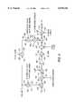
- FIG. 3diagrammatically illustrates a sequential, maximal descent, perturbational gradient search mechanism for processing the measure of intermodulation distortion.
- the inventionprimarily resides in what is effectively a prescribed arrangement of conventional communication circuits and associated digital signal processing components and attendant supervisory control routines, that control the operations of such circuits and components.
- the configuration of such circuits and components and the manner in which they are interfaced with other communication system equipmenthave, for the most part, been illustrated in the drawings by readily understandable block diagrams, which show only those specific details that are pertinent to the present invention, so as not to obscure the disclosure with details which will be readily apparent to those skilled in the art having the benefit of the description herein.
- the block diagram illustrationsare primarily intended to present the major components of the system in a convenient functional grouping and signal processing sequence, whereby the present invention may be more readily understood.
- FIG. 1The architecture of a non-linear RF power amplifier architecture, which incorporates the aliased wide band performance monitor of the present invention, is diagrammatically illustrated in FIG. 1 as comprising an RF input port 11, to which an RF signal to be amplified by a non-linear RF amplifier 10 is coupled.
- the RF input port 11is coupled to a first RF signal flow path 21 that includes an adaptive predistortion unit 23 and a first vector modulator 25 of a preamplification signal processing loop 20.
- Adaptive predistortion unit 23which may comprise a set of RF gain and phase adjustment weights, is coupled to receive a set of weighting coefficients w 0 , w 1 , w 2 , . . .
- vector modulator 25which may comprise an RF amplitude and phase adjustment circuit, has respective amplitude/gain (G) and phase ( ⁇ ) control inputs 26 and 27, to which first amplitude and phase adjustment signals (G 1 , ⁇ 1 ) are supplied by DSP 100, as will be described. These control signals cause the vector modulator 25 to maximize cancellation of RF carrier signals, so as to leave only RF error.
- DSPperformance monitoring and parameter updating digital signal processor
- Input port 11is further coupled via a directional coupler 13 to a second RF signal flow path 22 of preamplification signal processing loop 20.
- Directional coupler 13thus extracts a portion of the input RF signal, prior to its being subjected to the non-linear amplification operation of the RF amplifier 10.
- the preamplification signal processing loop 20includes a delay circuit 15, the output of which is coupled to a first port 31 of an RF carrier cancellation combiner 30 (e.g., a Wilkinson splitter/combiner, as a non-limiting example) of a feed-forward error extraction and reinjection loop 40.
- Delay circuit 15is operative to provide a delay corresponding to the insertion delay imparted to the first RF signal flow path 21 by the adaptive predistortion unit 23, vector modulator 25 and RF amplifier 10.
- a portion of the amplified signal output of the RF amplifier 10is extracted via a directional coupler 17 and coupled to a second port 32 of carrier cancellation combiner 30.
- the output of the directional coupler 17is representative of the amplified original RF input signal and any intermodulation (spectral regrowth) distortion products (IMDs) introduced by the non-linear RF amplifier 10.
- Cancellation combiner 30is operative to cancel the delayed (time aligned) RF carrier component supplied by the second RF signal flow path 22 from the output of the RF amplifier 10, and thus provide an RF error signal representative of the IMDs introduced by the RF amplifier 10.
- the RF error signal produced by RF cancellation combiner 30is coupled to a second vector modulator 35 of a feed-forward error correction and reinjection loop 40.
- the output of the vector modulator 35is amplified in a feed-forward error amplifier 38, and then reinjected into the output path 14 of the RF amplifier 10 by way of a reinjection directional coupler 16.
- Vector modulator 35has respective amplitude and phase control inputs 36 and 37, to which respective amplitude and phase adjustment signals (G 2 , ⁇ 2 ) are supplied by the digital signal processor 100, as will be described.
- the reinjection directional coupler 16is installed in the RF amplifier's output path 14, downstream of a delay unit 17 to which the output of RF amplifier 10 is coupled.
- Delay unit 17provides an effective delay corresponding to the insertion delay of the components in an RF error signal flow path 41 through the RF cancellation combiner 30, vector modulator 35 and error amplifier 38 of the feed-forward error contained in the feed-forward error correction and reinjection loop 40.
- the digital signal processor 100is coupled to each of the preamplification signal processing loop 20, and the feed-forward error correction and reinjection loop 40.
- a portion of the output of the RF carrier cancellation combiner 30is extracted via a directional coupler 19 and is supplied to a first input port 52 of a loop monitoring switch 50, an output port 53 of which is digitized by a sub-sampling wideband analog-to-digital converter 70 and supplied to DSP 100.
- the output of the directional coupler 19is representative of the intermodulation distortion products in the output of the RF amplifier 10.
- a portion of the composite signal in the RF amplifier's signal output path 14is extracted via a directional coupler 18 installed downstream of reinjection directional coupler 16, and is applied to a second input port 51 of switch 50.
- a portion of the RF signal flow path 22is coupled to a further input 54 of switch 50.
- these signalsare used by DSP 100 to adjust weighting coefficients (w 1 -w n ) supplied to the predistortion compensation unit 23 and the amplitude (G) and phase ( ⁇ ) control signals for each of vector modulators 25 and 35.
- the output port 53 of switch 50is coupled to a first port 61 of a mixer 60.
- a second port 62 of mixer 60is coupled to the output of a downconverting local oscillator 64.
- the (IF) output 66 of mixer 60is coupled through a low pass filter 67 and then digitized by a wideband analog-to-digital converter (ADC) 70, at a prescribed sampling rate and data resolution (e.g., 65 Ms/s, with a code width of twelve bits per sample, as a non-limiting example), which may be less than the bandwidth of the down converted (IF) signals plus distortion.
- ADCanalog-to-digital converter
- the sampling rate of the ADC 70is necessarily less than the Nyquist criterion (which is twice the bandwidth of the signals being sampled).
- the digitized sub-sampled datais actually an aliased signal--hence, the term ⁇ aliased ⁇ wideband performance monitor of the present invention.
- the digitized sample data produced by ADC 70is buffered through a first-in, first-out (FIFO) serial buffer 75, so that it may be transferred at a data rate that is compatible with the processing speed of digital signal processor 100.
- FIFOfirst-in, first-out
- buffer 75are controllably coupled to DSP 100 in prescribed sets or blocks (e.g., 4096 samples per block, as a non-limiting example) to digital signal processor 100, under the control of a transfer request signal applied over a transfer control line 102 from a write-read control unit 80, such as a complex programmable logic device, which controls the sampling by ADC 70 and the data transfer through buffer 75 in accordance with a local clock circuit 85.
- a write-read control unit 80such as a complex programmable logic device
- successive blocks of sampled dataare controllably coupled from the FIFO buffer 75 into DSP 100, they are processed in accordance with performance monitoring and control parameter updating processing routines resident in DSP 100 (to be described below with reference to FIGS. 2-3), so as to update the weighting coefficients w 0 , w 1 , w 2 , . . . , w N to the predistortion compensation unit 23, and the two sets of amplitude and phase control signals (G 1 , ⁇ 1 , G 2 , ⁇ 2 ) for vector modulators 25 and 35, as will be described.
- DACdigital-to-analog converter
- the performance monitoring routine executed by DSP 100for controlling the operation of the RF signal processing architecture of FIG. 1, is operative to process a respective block D of data (4096 samples) read out of FIFO buffer 75.
- a conventional Fast Fourier TransformFFT may be employed.
- the window functionaids in the dynamic range of the spectrum of transferred samples.
- the window function WINmay comprise a conventional Blackman-Harris window function. Described below are signal processing operations carried out by processor 100 for deriving gain and phase parameters for vector modulator 25 of the preamplification signal processing loop 20 and for the vector modulator 35 of feed-forward error extraction and reinjection loop 40, and for deriving weighting coefficients for predistortion unit 23 of the preamplification signal processing loop 20.
- the output port 53 of switch 50is initially set to input port 54, which is coupled to the signal flow path 22 via directional coupler 24.
- the spectrumis evaluated and a carrier (sensitivity) mask Mnew is defined.
- a carrier (sensitivity) mask Mnewis defined.
- an average mask value Maveis set equal to a previous mask value Mold*A+(1-A)*Mnew, where A is a constant less than 1.
- the output port 53 of switch 50is coupled to input port 52, so as to monitor the output of RF carrier cancellation combiner 30 via directional coupler 19.
- datais collected from the output of the combiner 30, and the spectrum is reevaluated.
- the spectrum data("Si" samples) are multiplied by (1-Mi), so as to effectively leave only the carrier power in the resulting sum.
- the gain and phase control parameters (G 1 and ⁇ 1 ) for the vector modulator 25are then adjusted so as to minimize carrier power, using a perturbational algorithm, such as a sequential, maximal descent, perturbational gradient search algorithm, to be described below with reference to FIG. 3.
- the output port 53 of switch 50is again initially set to input port 51, which is coupled to the amplified signal output path 14, via directional coupler 18.
- the spectrumis evaluated and a carrier mask Mnew is defined.
- an average mask value Maveis set equal to a previous mask value Mold*A+(1-A)*Mnew, where A is a constant less than 1.
- the output port 53 of the switch 50is maintained at input port 51.
- datais collected from the output of directional coupler 18, and the spectrum is evaluated.
- the spectrum data("Si" samples) are multiplied by Mi, so as to effectively leave only the intermodulation distortion power in the resulting sum P as follows: ##EQU2##
- Nis the number of spectrum samples.
- the gain and phase control parameters (G 2 and ⁇ 2 ) for the vector modulator 35are then adjusted so as to minimize or maximally cancel the intermodulation distortion power, using a perturbational algorithm, such as that shown in FIG. 3, to be described.
- the output port 53 of switch 50is again initially set to input port 54, which is coupled to the signal flow path 22 via directional coupler 24.
- the spectrumis evaluated and a carrier mask Mnew is defined.
- the output port 53 of switch 50is then coupled to input port 52, so as to monitor the output of RF carrier cancellation combiner 30.
- datais collected from the output of combiner 30 via directional coupler 19, and the spectrum is evaluated.
- the spectrum data(“Si" samples) are multiplied by Mave, so as to effectively leave only intermodulation power in the resulting sum P.
- the predistortion weights w i , . . . , w nare then adjusted to minimize the resulting sum, using a perturbational algorithm, such as that shown in FIG. 3, to be described.
- the sensitivity mask function Mis generated in accordance with the signal processing routine shown in the flow chart of FIG. 2.
- step 201time domain samples y i are multiplied by a time domain window function WIN to obtain y i *WIN.
- FFTFast Fourier Transform
- the value of S iis compared with the upper and lower limit values T U and T L . As long as S i falls between the upper and lower limits, namely T L ⁇ S i ⁇ T U , M i is set at a value of 1 (step 207). Otherwise, in step 208, M i is set to a value of 0.
- FIG. 3diagrammatically illustrates a sequential, maximal descent, perturbational gradient search mechanism, to which the IMD power P derived as described above is applied, for controllably adjusting or updating respective ones of the predistortion weight parameters w 1 -w n , and the vector modulator gain and phase parameters G and ⁇ .
- the error power Pis applied as a first input 401 to a multiplication operator 400, a second input 402 is coupled to the product output 413 of an adaptation multiplier 410.
- Multiplier 410has a first input 411 coupled to receive a loop gain parameter (loop -- gain), which is normally a constant and serves to control the speed of adaptation of the gradient search.
- loop -- gainloop gain parameter
- a second input 412 of multiplier 410is coupled to receive a correlation control parameter (0 for a fixed, manual setting, or 1 for adaptive operation).
- the loop -- gain valueis further coupled to a first input 421 of a scaling multiplier 420, a second input of which receives a parameter equal to the difference between 1.0 and a dc -- scale value.
- the parameter dc -- scaleis used to establish the step size of the gradient search.
- the output 403 of multiplier 400is coupled to a first input 431 of a correlation sequence multiplier 430, a second input 412 of which receives a correlation sequence control input (+/-1), that is operative to provide negative feedback.
- the output 433 of multiplier 430is coupled to a first input 441 of a multiplier 440, a second input 442 of which is coupled to receive the parameter x -- gain, a stabilizing scaling factor, similar to loop -- gain, where ⁇ x ⁇ corresponds to parameter of interest (w, G or ⁇ ) being controlled/adjusted.
- the output 443 of multiplier 440is integrated at 444 and applied as a first input 451 to a scaling multiplier 450.
- a second input 452 of multiplier 450is coupled to receive the dc -- scale value which, as noted above, is used to control the step size of the gradient search.
- the output 453 of scaling multiplier 450is controllably gated through a latch 455 in accordance with a cycle clock, that determines how often the new adapted parameter value of interest (x) is coupled to the DAC 120, so as to be applied therefrom to one of the predistortion unit 23, and vector modulators 25 and 35.
- the updated value of xis coupled to a first input 461 of an adder 460.
- a second input 462 of adder 460is coupled to the output 473 of a correlation sequence multiplier 470, a first input 471 of which receives a correlation sequence control input (-/+1), which is opposite to that applied to correlation sequence multiplier 430, described above.
- a second input 472 of multiplier 470is coupled to the output 483 of a perturbation scaling multiplier 480, a first input 481 of which is coupled to the output 423 of scaling multiplier 420.
- Multiplier 480has a second input 482 coupled to receive a perturbation control parameter (0 for a fixed, manual setting, or 1 for adaptive operation).
- the output 463 of adder 460is coupled to a first input 491 of a multiplier 490 which effectively serves as a switch control function for controllably coupling the updated parameter ⁇ x ⁇ to the associated input of the respectively adjusted component of the RF signal processing architecture of FIG. 1.
- a second (binary) input 492 of multiplier 490receives either 1 or 0, in accordance with whether or not the control parameter is to be updated.
- the output 493 of multiplier 490is coupled to DAC 120, which provides a corresponding analog voltage to an associated control input of one of the predistortion unit 23, and vector modulators 25 and 35.
- the frequency at which the control parameters (w 1 -w n , G 1 and ⁇ 1 ) of the preamplification signal processing loop 20, and (G 2 and ⁇ 2 ) of the feed-forward error correction and reinjection loop 40 are updatedis determined in accordance with the operation of the loop monitoring switch 50.
- Setting the initial values for and adjusting the sensitivity mask, as well as the gain and phase control values G 2 , ⁇ 2 for the vector modulator 35 of the feed-forward error correction and reinjection loop 40is performed by providing throughput connectivity between ports 51 and 53 of the switch, thereby coupling data representative of the composite RF signal, subsequent to error signal reinjection in the RF amplifier's signal output path 14, to the DSP 100.
- Updating the weighting coefficients w for the adaptive predistortion unit 23 and the gain and phase control values G 1 , ⁇ 1 for the vector modulator 25 of the preamplification signal processing loop 20is performed by providing throughput connectivity between ports 51 and 52 of the switch 50, thereby supplying intermodulation distortion products at the output of the RF carrier cancellation combiner 30 to ADC 70 for application to DSP 100.
- the rate at which connectivity through the switch 50 is changed between input ports 51 and 52is determined by the intended rate of adaptation and monitored error variation.
Landscapes
- Physics & Mathematics (AREA)
- Nonlinear Science (AREA)
- Engineering & Computer Science (AREA)
- Power Engineering (AREA)
- Amplifiers (AREA)
Abstract
Description
Claims (20)
Priority Applications (1)
| Application Number | Priority Date | Filing Date | Title |
|---|---|---|---|
| US09/053,529US6078216A (en) | 1998-03-31 | 1998-03-31 | Aliased wide band performance monitor for adjusting predistortion and vector modulator control parameters of RF amplifier |
Applications Claiming Priority (1)
| Application Number | Priority Date | Filing Date | Title |
|---|---|---|---|
| US09/053,529US6078216A (en) | 1998-03-31 | 1998-03-31 | Aliased wide band performance monitor for adjusting predistortion and vector modulator control parameters of RF amplifier |
Publications (1)
| Publication Number | Publication Date |
|---|---|
| US6078216Atrue US6078216A (en) | 2000-06-20 |
Family
ID=21984903
Family Applications (1)
| Application Number | Title | Priority Date | Filing Date |
|---|---|---|---|
| US09/053,529Expired - LifetimeUS6078216A (en) | 1998-03-31 | 1998-03-31 | Aliased wide band performance monitor for adjusting predistortion and vector modulator control parameters of RF amplifier |
Country Status (1)
| Country | Link |
|---|---|
| US (1) | US6078216A (en) |
Cited By (49)
| Publication number | Priority date | Publication date | Assignee | Title |
|---|---|---|---|---|
| US6232838B1 (en)* | 1999-08-10 | 2001-05-15 | Nec Corporation | Feed-forward amplifier and method of compensating non-linear distortion in the same |
| WO2002015389A1 (en)* | 2000-08-17 | 2002-02-21 | Spectrian Corporation | Distortion detection apparatus for controlling predistortion, carrier cancellation and feed-forward cancellation in linear rf power amplifiers |
| US20020048326A1 (en)* | 2000-08-29 | 2002-04-25 | Sahlman Karl-Gosta Emanuel | Method and apparatus for plurality signal generation |
| US6384681B1 (en)* | 2000-01-07 | 2002-05-07 | Spectrian Corporation | Swept performance monitor for measuring and correcting RF power amplifier distortion |
| US6392481B1 (en)* | 1999-11-30 | 2002-05-21 | Nokia Networks Oy | Method and apparatus for improved fed forward amplification |
| US6407635B2 (en) | 2000-01-07 | 2002-06-18 | Spectrian Corporation | Carrier-blanking mechanism for sweeping detector used to measure and correct RF power amplifier distortion |
| US20020168025A1 (en)* | 2001-05-14 | 2002-11-14 | Schwent Dale G. | Multiple bandwidth amplifier control systems for mobile stations and methods therefor |
| US20030001669A1 (en)* | 2001-06-29 | 2003-01-02 | Mark Billsberry | Balanced distortion reduction circuit |
| US6522198B2 (en)* | 1999-12-15 | 2003-02-18 | Lg Electronics Inc. | Power amplifier having predistortion linearizer |
| US6525603B1 (en)* | 2001-01-05 | 2003-02-25 | Remec, Inc. | Feedforward amplifier linearization adapting off modulation |
| US20030058960A1 (en)* | 2001-09-21 | 2003-03-27 | Lg Electronics Inc. | Predistortion type-linearized power amplification system using digital if technology |
| US6593806B1 (en)* | 2001-08-10 | 2003-07-15 | Cirrus Logic, Inc. | Circuits and methods for compensating switched mode amplifiers |
| US20040017256A1 (en)* | 2002-07-25 | 2004-01-29 | Bumman Kim | Linearization apparatus capable of adjusting peak-to-average power ratio |
| US6697436B1 (en)* | 1999-07-13 | 2004-02-24 | Pmc-Sierra, Inc. | Transmission antenna array system with predistortion |
| KR20040017166A (en)* | 2002-08-20 | 2004-02-26 | 알에프코어 주식회사 | Rf linear power amplifier |
| US6700439B2 (en) | 2002-04-11 | 2004-03-02 | Andrew Corporation | Zero-bias bypass switch |
| EP1079517A3 (en)* | 1999-08-19 | 2004-05-19 | Lucent Technologies Inc. | Adaptive gain and/or phase adjustment control system and method |
| US20040109697A1 (en)* | 2000-01-06 | 2004-06-10 | Adc Telecommunications, Inc. | Dynamic distortion control |
| US20040136470A1 (en)* | 2003-01-15 | 2004-07-15 | Andrew Corporation | Uncorrelated adaptive predistorter |
| US6794933B2 (en) | 2002-02-14 | 2004-09-21 | Powerwave Technologies, Inc. | Fast forward RF power amplifier with high efficiency main amplifier and highly linear error amplifier |
| US6798843B1 (en) | 1999-07-13 | 2004-09-28 | Pmc-Sierra, Inc. | Wideband digital predistortion linearizer for nonlinear amplifiers |
| US6812786B2 (en) | 2002-04-11 | 2004-11-02 | Andrew Corporation | Zero-bias bypass switching circuit using mismatched 90 degrees hybrid |
| US20040232985A1 (en)* | 2002-05-14 | 2004-11-25 | Hiroshi Itahara | Hybrid distortion compensation method and hybrid distortion compensation device |
| US20050017801A1 (en)* | 2003-07-23 | 2005-01-27 | Andrew Corporation | Elimination of peak clipping and improved efficiency for RF power amplifiers with a predistorter |
| US20050174173A1 (en)* | 2002-06-25 | 2005-08-11 | Blodgett James R. | Forward amplifiers |
| US20050200409A1 (en)* | 2004-03-11 | 2005-09-15 | Braithwaite Richard N. | System and method for control of loop alignment in adaptive feed forward amplifiers |
| US7085330B1 (en) | 2002-02-15 | 2006-08-01 | Marvell International Ltd. | Method and apparatus for amplifier linearization using adaptive predistortion |
| US20060217083A1 (en)* | 2005-03-22 | 2006-09-28 | Braithwaite Richard N | Rf power amplifier system employing an analog predistortion module using zero crossings |
| US20070116100A1 (en)* | 2005-11-21 | 2007-05-24 | Telefonaktiebolaget Lm Ericsson (Publ) | Simplified generalized rake receiver method and apparatus |
| US7362821B1 (en) | 2002-05-22 | 2008-04-22 | Marvel International Ltd. | Method and apparatus for amplifier linearization using adaptive predistortion |
| US20080211576A1 (en)* | 2007-02-26 | 2008-09-04 | Harris Corporation | Linearization of RF Power Amplifiers Using an Adaptive Subband Predistorter |
| US20080218262A1 (en)* | 2007-03-09 | 2008-09-11 | Alcatel Lucent | Predistortion with asymmetric usage of available bandwidth |
| US20080252371A1 (en)* | 2007-04-16 | 2008-10-16 | Takeshi Ishigami | Feedforward amplifier |
| US20090251211A1 (en)* | 2008-04-02 | 2009-10-08 | Harris Corporation | Feedforward linearization of rf power amplifiers |
| EP2178206A2 (en) | 2008-10-17 | 2010-04-21 | Fraunhofer-Gesellschaft zur Förderung der angewandten Forschung e.V. | Feed-forward amplifier with device for creating a correction signal |
| US20110064155A1 (en)* | 2008-05-28 | 2011-03-17 | Junya Ashita | distortion compensation circuit and a distortion compensation method |
| US8498591B1 (en) | 2009-08-21 | 2013-07-30 | Marvell International Ltd. | Digital Predistortion for nonlinear RF power amplifiers |
| US8699620B1 (en) | 2010-04-16 | 2014-04-15 | Marvell International Ltd. | Digital Predistortion for nonlinear RF power amplifiers |
| US20140161207A1 (en)* | 2012-12-07 | 2014-06-12 | Maxim Integrated Products, Inc. | Digital pre-distortion system for radio frequency transmitters with reduced sampling rate in observation loop |
| US9160586B1 (en) | 2013-07-24 | 2015-10-13 | Marvell International Ltd. | Method and apparatus for estimating and compensating for in-phase and quadrature (IQ) mismatch in a receiver of a wireless communication device |
| US10637415B1 (en) | 2018-11-16 | 2020-04-28 | Industrial Technology Research Institute | Linearity improving system and linearity improving method |
| CN112737645A (en)* | 2019-10-14 | 2021-04-30 | 财团法人工业技术研究院 | Transmitter using hybrid beamforming and performing code division feedback for digital predistortion |
| US11296900B2 (en) | 2005-03-25 | 2022-04-05 | Neo Wireless Llc | Broadcast signal indicating one or more subframe configurations |
| US11324049B2 (en) | 2004-03-09 | 2022-05-03 | Neo Wireless Llc | Methods and apparatus for random access in multi-carrier communication systems |
| US11368347B2 (en) | 2004-01-29 | 2022-06-21 | Neo Wireless Llc | Channel probing signal for a broadband communication system |
| US11388034B2 (en) | 2004-01-29 | 2022-07-12 | Neo Wireless Llc | Method and apparatus using cell-specific and common pilot subcarriers in multi-carrier, multi-cell wireless communication networks |
| US11483832B1 (en) | 2010-09-28 | 2022-10-25 | Neo Wireless Llc | Methods and apparatus for flexible use of frequency bands |
| US11496259B2 (en) | 2004-02-13 | 2022-11-08 | Neo Wireless Llc | Methods and apparatus for multi-carrier communication systems with adaptive transmission and feedback |
| US11979248B2 (en) | 2005-06-09 | 2024-05-07 | Neo Wireless Llc | Method and apparatus for receiving broadcast information in an OFDM communication system |
Citations (2)
| Publication number | Priority date | Publication date | Assignee | Title |
|---|---|---|---|---|
| US5485120A (en)* | 1994-07-28 | 1996-01-16 | Aval Communications Inc. | Feed-forward power amplifier system with adaptive control and control method |
| US5515000A (en)* | 1994-05-31 | 1996-05-07 | Fujitsu Limited | Feed-forward amplifier of a type preventing unwanted waves from being outputted in the initial operation |
- 1998
- 1998-03-31USUS09/053,529patent/US6078216A/ennot_activeExpired - Lifetime
Patent Citations (2)
| Publication number | Priority date | Publication date | Assignee | Title |
|---|---|---|---|---|
| US5515000A (en)* | 1994-05-31 | 1996-05-07 | Fujitsu Limited | Feed-forward amplifier of a type preventing unwanted waves from being outputted in the initial operation |
| US5485120A (en)* | 1994-07-28 | 1996-01-16 | Aval Communications Inc. | Feed-forward power amplifier system with adaptive control and control method |
Non-Patent Citations (2)
| Title |
|---|
| Grant et al. "A DSP Controlled Adaptive Feedforward Amplifier Linearizer" IEEE pp 788-792, 1996. |
| Grant et al. A DSP Controlled Adaptive Feedforward Amplifier Linearizer IEEE pp 788 792, 1996.* |
Cited By (93)
| Publication number | Priority date | Publication date | Assignee | Title |
|---|---|---|---|---|
| US6798843B1 (en) | 1999-07-13 | 2004-09-28 | Pmc-Sierra, Inc. | Wideband digital predistortion linearizer for nonlinear amplifiers |
| US6697436B1 (en)* | 1999-07-13 | 2004-02-24 | Pmc-Sierra, Inc. | Transmission antenna array system with predistortion |
| US6232838B1 (en)* | 1999-08-10 | 2001-05-15 | Nec Corporation | Feed-forward amplifier and method of compensating non-linear distortion in the same |
| EP1079517A3 (en)* | 1999-08-19 | 2004-05-19 | Lucent Technologies Inc. | Adaptive gain and/or phase adjustment control system and method |
| US6392481B1 (en)* | 1999-11-30 | 2002-05-21 | Nokia Networks Oy | Method and apparatus for improved fed forward amplification |
| US6522198B2 (en)* | 1999-12-15 | 2003-02-18 | Lg Electronics Inc. | Power amplifier having predistortion linearizer |
| US20040109697A1 (en)* | 2000-01-06 | 2004-06-10 | Adc Telecommunications, Inc. | Dynamic distortion control |
| US7155132B2 (en)* | 2000-01-06 | 2006-12-26 | Adc Telecommunications, Inc. | Dynamic distortion control |
| US6407635B2 (en) | 2000-01-07 | 2002-06-18 | Spectrian Corporation | Carrier-blanking mechanism for sweeping detector used to measure and correct RF power amplifier distortion |
| US6384681B1 (en)* | 2000-01-07 | 2002-05-07 | Spectrian Corporation | Swept performance monitor for measuring and correcting RF power amplifier distortion |
| WO2002015389A1 (en)* | 2000-08-17 | 2002-02-21 | Spectrian Corporation | Distortion detection apparatus for controlling predistortion, carrier cancellation and feed-forward cancellation in linear rf power amplifiers |
| US6359508B1 (en) | 2000-08-17 | 2002-03-19 | Spectrian Corporation | Distortion detection apparatus for controlling predistortion, carrier cancellation and feed-forward cancellation in linear RF power amplifiers |
| US6934341B2 (en)* | 2000-08-29 | 2005-08-23 | Telefonaktiebolaget Lm Ericsson (Publ) | Method and apparatus for plurality signal generation |
| US20020048326A1 (en)* | 2000-08-29 | 2002-04-25 | Sahlman Karl-Gosta Emanuel | Method and apparatus for plurality signal generation |
| US6525603B1 (en)* | 2001-01-05 | 2003-02-25 | Remec, Inc. | Feedforward amplifier linearization adapting off modulation |
| US6850574B2 (en)* | 2001-05-14 | 2005-02-01 | Motorola, Inc. | Multiple bandwidth amplifier control systems for mobile stations and methods therefor |
| US20020168025A1 (en)* | 2001-05-14 | 2002-11-14 | Schwent Dale G. | Multiple bandwidth amplifier control systems for mobile stations and methods therefor |
| US20030001669A1 (en)* | 2001-06-29 | 2003-01-02 | Mark Billsberry | Balanced distortion reduction circuit |
| US6734726B2 (en) | 2001-06-29 | 2004-05-11 | Remec, Inc. | Balanced distortion reduction circuit |
| US6593806B1 (en)* | 2001-08-10 | 2003-07-15 | Cirrus Logic, Inc. | Circuits and methods for compensating switched mode amplifiers |
| US20030058960A1 (en)* | 2001-09-21 | 2003-03-27 | Lg Electronics Inc. | Predistortion type-linearized power amplification system using digital if technology |
| US6794933B2 (en) | 2002-02-14 | 2004-09-21 | Powerwave Technologies, Inc. | Fast forward RF power amplifier with high efficiency main amplifier and highly linear error amplifier |
| US7535974B1 (en) | 2002-02-15 | 2009-05-19 | Marvell International Ltd. | Method and apparatus for amplifier linearization using adaptive predistortion |
| US7085330B1 (en) | 2002-02-15 | 2006-08-01 | Marvell International Ltd. | Method and apparatus for amplifier linearization using adaptive predistortion |
| US6812786B2 (en) | 2002-04-11 | 2004-11-02 | Andrew Corporation | Zero-bias bypass switching circuit using mismatched 90 degrees hybrid |
| US6700439B2 (en) | 2002-04-11 | 2004-03-02 | Andrew Corporation | Zero-bias bypass switch |
| CN100359801C (en)* | 2002-05-14 | 2008-01-02 | 松下电器产业株式会社 | Mixed distortion compensation method and mixed distortion compensation device |
| US20040232985A1 (en)* | 2002-05-14 | 2004-11-25 | Hiroshi Itahara | Hybrid distortion compensation method and hybrid distortion compensation device |
| US7248112B2 (en) | 2002-05-14 | 2007-07-24 | Matsushita Electric Industrial Co., Ltd. | Hybrid distortion compensation method and hybrid distortion compensation device |
| US7362821B1 (en) | 2002-05-22 | 2008-04-22 | Marvel International Ltd. | Method and apparatus for amplifier linearization using adaptive predistortion |
| US7342446B2 (en)* | 2002-06-25 | 2008-03-11 | Soma Networks, Inc. | Apparatus and method for controlling feed-forward amplifiers |
| US20050174173A1 (en)* | 2002-06-25 | 2005-08-11 | Blodgett James R. | Forward amplifiers |
| US20040017256A1 (en)* | 2002-07-25 | 2004-01-29 | Bumman Kim | Linearization apparatus capable of adjusting peak-to-average power ratio |
| US6867648B2 (en)* | 2002-07-25 | 2005-03-15 | Postech Foundation | Linearization apparatus capable of adjusting peak-to-average power ratio |
| KR20040017166A (en)* | 2002-08-20 | 2004-02-26 | 알에프코어 주식회사 | Rf linear power amplifier |
| DE102004002239B4 (en)* | 2003-01-15 | 2015-06-25 | Andrew Ag | Uncorrelated adaptive predistorter |
| KR101107866B1 (en) | 2003-01-15 | 2012-01-31 | 앤드류 엘엘씨 | Correlation Adaptive Precompensator |
| US7403573B2 (en)* | 2003-01-15 | 2008-07-22 | Andrew Corporation | Uncorrelated adaptive predistorter |
| US20040136470A1 (en)* | 2003-01-15 | 2004-07-15 | Andrew Corporation | Uncorrelated adaptive predistorter |
| GB2398683B (en)* | 2003-01-15 | 2007-08-29 | Andrew Corp | An uncorrelated adaptive predistorter |
| GB2398683A (en)* | 2003-01-15 | 2004-08-25 | Andrew Corp | An uncorrelated adaptive predistorter for an RF power amplifier in a mobile phone system |
| US7259630B2 (en) | 2003-07-23 | 2007-08-21 | Andrew Corporation | Elimination of peak clipping and improved efficiency for RF power amplifiers with a predistorter |
| US20050017801A1 (en)* | 2003-07-23 | 2005-01-27 | Andrew Corporation | Elimination of peak clipping and improved efficiency for RF power amplifiers with a predistorter |
| US11368347B2 (en) | 2004-01-29 | 2022-06-21 | Neo Wireless Llc | Channel probing signal for a broadband communication system |
| US11388034B2 (en) | 2004-01-29 | 2022-07-12 | Neo Wireless Llc | Method and apparatus using cell-specific and common pilot subcarriers in multi-carrier, multi-cell wireless communication networks |
| US11804870B2 (en) | 2004-01-29 | 2023-10-31 | Neo Wireless Llc | Channel probing signal for a broadband communication system |
| US11522650B2 (en) | 2004-02-13 | 2022-12-06 | Neo Wireless Llc | Methods and apparatus for multi-carrier communication systems with adaptive transmission and feedback |
| US11683136B2 (en) | 2004-02-13 | 2023-06-20 | Neo Wireless Llc | Methods and apparatus for multi-carrier communication systems with adaptive transmission and feedback |
| US11496259B2 (en) | 2004-02-13 | 2022-11-08 | Neo Wireless Llc | Methods and apparatus for multi-carrier communication systems with adaptive transmission and feedback |
| US12003439B2 (en) | 2004-02-13 | 2024-06-04 | Neo Wireless Llc | Methods and apparatus for multi-carrier communication systems with adaptive transmission and feedback |
| US12368624B2 (en) | 2004-03-09 | 2025-07-22 | Neo Wireless Llc | Methods and apparatus for random access in multi-carrier communication systems |
| US11324049B2 (en) | 2004-03-09 | 2022-05-03 | Neo Wireless Llc | Methods and apparatus for random access in multi-carrier communication systems |
| US11502888B2 (en) | 2004-03-09 | 2022-11-15 | Neo Wireless Llc | Methods and apparatus for random access in multi-carrier communication systems |
| US20050200409A1 (en)* | 2004-03-11 | 2005-09-15 | Braithwaite Richard N. | System and method for control of loop alignment in adaptive feed forward amplifiers |
| US7157967B2 (en) | 2004-03-11 | 2007-01-02 | Powerwave Technologies Inc. | System and method for control of loop alignment in adaptive feed forward amplifiers |
| US7193462B2 (en) | 2005-03-22 | 2007-03-20 | Powerwave Technologies, Inc. | RF power amplifier system employing an analog predistortion module using zero crossings |
| US20060217083A1 (en)* | 2005-03-22 | 2006-09-28 | Braithwaite Richard N | Rf power amplifier system employing an analog predistortion module using zero crossings |
| US11658838B2 (en) | 2005-03-25 | 2023-05-23 | Neo Wireless Llc | Broadcast signal indicating one or more subframe configurations |
| US11296900B2 (en) | 2005-03-25 | 2022-04-05 | Neo Wireless Llc | Broadcast signal indicating one or more subframe configurations |
| US11979248B2 (en) | 2005-06-09 | 2024-05-07 | Neo Wireless Llc | Method and apparatus for receiving broadcast information in an OFDM communication system |
| US12284049B2 (en) | 2005-06-09 | 2025-04-22 | Neo Wireless Llc | Methods and apparatus for power efficient broadcasting and communication systems |
| US20070116100A1 (en)* | 2005-11-21 | 2007-05-24 | Telefonaktiebolaget Lm Ericsson (Publ) | Simplified generalized rake receiver method and apparatus |
| US8019015B2 (en)* | 2007-02-26 | 2011-09-13 | Harris Corporation | Linearization of RF power amplifiers using an adaptive subband predistorter |
| US20080211576A1 (en)* | 2007-02-26 | 2008-09-04 | Harris Corporation | Linearization of RF Power Amplifiers Using an Adaptive Subband Predistorter |
| US20080218262A1 (en)* | 2007-03-09 | 2008-09-11 | Alcatel Lucent | Predistortion with asymmetric usage of available bandwidth |
| US7679440B2 (en)* | 2007-04-16 | 2010-03-16 | Hitachi Kokusai Electric Inc. | Feedforward amplifier |
| US20080252371A1 (en)* | 2007-04-16 | 2008-10-16 | Takeshi Ishigami | Feedforward amplifier |
| US20090251211A1 (en)* | 2008-04-02 | 2009-10-08 | Harris Corporation | Feedforward linearization of rf power amplifiers |
| US7642850B2 (en) | 2008-04-02 | 2010-01-05 | Harris Corporation | Feedforward linearization of RF power amplifiers |
| US20110064155A1 (en)* | 2008-05-28 | 2011-03-17 | Junya Ashita | distortion compensation circuit and a distortion compensation method |
| US8446980B2 (en)* | 2008-05-28 | 2013-05-21 | Nec Corporation | Distortion compensation circuit and a distortion compensation method |
| US7940106B2 (en) | 2008-10-17 | 2011-05-10 | Fraunhofer-Gesellschaft Zur Foerderung Der Angewandten Forschung E.V. | Apparatus for generating a correction signal |
| EP2178206A2 (en) | 2008-10-17 | 2010-04-21 | Fraunhofer-Gesellschaft zur Förderung der angewandten Forschung e.V. | Feed-forward amplifier with device for creating a correction signal |
| US20100097134A1 (en)* | 2008-10-17 | 2010-04-22 | Fraunhofer-Gesellschaft Zur Forderung Der Angewandten Forschung E.V. | Apparatus for generating a correction signal |
| DE102008052172A1 (en) | 2008-10-17 | 2010-04-22 | Fraunhofer-Gesellschaft zur Förderung der angewandten Forschung e.V. | Device for generating a correction signal |
| US8498591B1 (en) | 2009-08-21 | 2013-07-30 | Marvell International Ltd. | Digital Predistortion for nonlinear RF power amplifiers |
| US9002302B1 (en) | 2009-08-21 | 2015-04-07 | Marvell International Ltd. | Digital Predistortion for nonlinear RF power amplifiers |
| US8699620B1 (en) | 2010-04-16 | 2014-04-15 | Marvell International Ltd. | Digital Predistortion for nonlinear RF power amplifiers |
| US8995572B1 (en) | 2010-04-16 | 2015-03-31 | Marvell International Ltd. | Digital Predistortion for nonlinear RF power amplifiers |
| US11483832B1 (en) | 2010-09-28 | 2022-10-25 | Neo Wireless Llc | Methods and apparatus for flexible use of frequency bands |
| US11510201B2 (en) | 2010-09-28 | 2022-11-22 | Neo Wireless Llc | Methods and apparatus for flexible use of frequency bands |
| US11510202B2 (en) | 2010-09-28 | 2022-11-22 | Neo Wireless Llc | Methods and apparatus for flexible use of frequency bands |
| US11985646B2 (en) | 2010-09-28 | 2024-05-14 | Neo Wireless Llc | Methods and apparatus for flexible use of frequency bands |
| US9014299B2 (en)* | 2012-12-07 | 2015-04-21 | Maxim Integrated Products, Inc. | Digital pre-distortion system for radio frequency transmitters with reduced sampling rate in observation loop |
| US20140161207A1 (en)* | 2012-12-07 | 2014-06-12 | Maxim Integrated Products, Inc. | Digital pre-distortion system for radio frequency transmitters with reduced sampling rate in observation loop |
| CN103873407A (en)* | 2012-12-07 | 2014-06-18 | 马克西姆综合产品公司 | Digital pre-distortion system for radio frequency transmitters with reduced sampling rate in observation loop |
| CN103873407B (en)* | 2012-12-07 | 2018-07-31 | 马克西姆综合产品公司 | Digital pre-distortion system for having the radiofrequency launcher of the sample rate reduced in observation ring |
| US9160586B1 (en) | 2013-07-24 | 2015-10-13 | Marvell International Ltd. | Method and apparatus for estimating and compensating for in-phase and quadrature (IQ) mismatch in a receiver of a wireless communication device |
| TWI696344B (en)* | 2018-11-16 | 2020-06-11 | 財團法人工業技術研究院 | Linearity improving system and linearity improving method |
| CN111200404B (en)* | 2018-11-16 | 2023-07-11 | 财团法人工业技术研究院 | Linearity improvement system and linearity improvement method |
| CN111200404A (en)* | 2018-11-16 | 2020-05-26 | 财团法人工业技术研究院 | Linearity improving system and linearity improving method |
| US10637415B1 (en) | 2018-11-16 | 2020-04-28 | Industrial Technology Research Institute | Linearity improving system and linearity improving method |
| CN112737645A (en)* | 2019-10-14 | 2021-04-30 | 财团法人工业技术研究院 | Transmitter using hybrid beamforming and performing code division feedback for digital predistortion |
Similar Documents
| Publication | Publication Date | Title |
|---|---|---|
| US6078216A (en) | Aliased wide band performance monitor for adjusting predistortion and vector modulator control parameters of RF amplifier | |
| US5760646A (en) | Feed-forward correction loop with adaptive predistortion injection for linearization of RF power amplifier | |
| KR100356250B1 (en) | Feed forward amplifier with digital intermodulation control | |
| US5929704A (en) | Control of RF error extraction using auto-calibrating RF correlator | |
| EP0890218B1 (en) | Adaptive amplifier distortion compensation circuit | |
| EP1262017B1 (en) | Spectral distortion monitor for controlling pre-distortion and feed-forward linearization of rf power amplifier | |
| WO1998004034A9 (en) | Rf amplifier having adaptative predistortion circuit | |
| US5594385A (en) | Ultra-linear feedforward amplifier with adaptive control and method for adaptive control | |
| US5610554A (en) | Cancellation loop, for a feed-forward amplifier, employing an adaptive controller | |
| US9461698B2 (en) | Communications device with simultaneous transmit and receive and related methods | |
| US8902724B2 (en) | Method and apparatus for cross-talk cancellation | |
| KR101077349B1 (en) | Linearization of rf power amplifiers using an adaptive subband predistorter | |
| US5949283A (en) | Adaptive digital predistortion linearization and feed-forward correction of RF power amplifier | |
| EP1505723B1 (en) | Hybrid distortion compensation method and hybrid distortion compensation apparatus | |
| US6407635B2 (en) | Carrier-blanking mechanism for sweeping detector used to measure and correct RF power amplifier distortion | |
| CA1134448A (en) | Adaptive interference suppression arrangement | |
| US20040021517A1 (en) | Power minimization, correlation-based closed loop for controlling predistorter and vector modulator feeding RF power amplifier | |
| WO2002015389A1 (en) | Distortion detection apparatus for controlling predistortion, carrier cancellation and feed-forward cancellation in linear rf power amplifiers | |
| Grant et al. | A DSP controlled adaptive feedforward amplifier linearizer | |
| KR20010071126A (en) | Distortion correction circuit for direct conversion receiver | |
| KR20020008456A (en) | Base station transmit unit with feed-forward mode linearization unit | |
| US5789927A (en) | Baseband measurement of RF power amplifier distortion | |
| KR100334236B1 (en) | Narrowband Interference Canceller System and its Method in CDMA System | |
| Lim et al. | Digital compensation in IQ modulators using adaptive FIR filters | |
| Yang et al. | Calibration of transmitter IQ imbalance with 1-bit feedback |
Legal Events
| Date | Code | Title | Description |
|---|---|---|---|
| AS | Assignment | Owner name:SPECTRIAN, CALIFORNIA Free format text:ASSIGNMENT OF ASSIGNORS INTEREST;ASSIGNOR:PROCTOR, JAMES ARTHUR JR.;REEL/FRAME:009078/0822 Effective date:19980325 | |
| STCF | Information on status: patent grant | Free format text:PATENTED CASE | |
| AS | Assignment | Owner name:SPECTRIAN CORPORATION, CALIFORNIA Free format text:CORRECTIVE ASSIGNMENT RE-RECORDED TO CORRECT THE COMPANY NAME SPECTRIAN CORPORATION PREVIOUSLY RECORDED ON REEL 9078, FRAME 0822;ASSIGNOR:PROCTOR, JAMES ARTHUR JR.;REEL/FRAME:011623/0775 Effective date:19980325 | |
| AS | Assignment | Owner name:REMEC, INC., CALIFORNIA Free format text:ASSIGNMENT OF ASSIGNORS INTEREST;ASSIGNOR:SPECTRIAN CORPORATION;REEL/FRAME:013949/0866 Effective date:20030324 | |
| FPAY | Fee payment | Year of fee payment:4 | |
| SULP | Surcharge for late payment | ||
| AS | Assignment | Owner name:POWERWAVE TECHNOLOGIES, INC., CALIFORNIA Free format text:ASSIGNMENT OF ASSIGNORS INTEREST;ASSIGNOR:REMEC, INC.;REEL/FRAME:017823/0684 Effective date:20051004 | |
| FPAY | Fee payment | Year of fee payment:8 | |
| FEPP | Fee payment procedure | Free format text:PAYOR NUMBER ASSIGNED (ORIGINAL EVENT CODE: ASPN); ENTITY STATUS OF PATENT OWNER: LARGE ENTITY | |
| AS | Assignment | Owner name:WELLS FARGO FOOTHILL, LLC, AS AGENT, CALIFORNIA Free format text:PATENT SECURITY AGREEMENT;ASSIGNOR:POWERWAVE TECHNOLOGIES, INC.;REEL/FRAME:022507/0027 Effective date:20090403 Owner name:WELLS FARGO FOOTHILL, LLC, AS AGENT,CALIFORNIA Free format text:PATENT SECURITY AGREEMENT;ASSIGNOR:POWERWAVE TECHNOLOGIES, INC.;REEL/FRAME:022507/0027 Effective date:20090403 | |
| REMI | Maintenance fee reminder mailed | ||
| FPAY | Fee payment | Year of fee payment:12 | |
| SULP | Surcharge for late payment | Year of fee payment:11 | |
| AS | Assignment | Owner name:POWERWAVE TECHNOLOGIES, INC., CALIFORNIA Free format text:RELEASE BY SECURED PARTY;ASSIGNOR:WELLS FARGO CAPITAL FINANCE, LLC, FKA WELLS FARGO FOOTHILL, LLC;REEL/FRAME:028819/0014 Effective date:20120820 | |
| AS | Assignment | Owner name:P-WAVE HOLDINGS, LLC, CALIFORNIA Free format text:SECURITY AGREEMENT;ASSIGNOR:POWERWAVE TECHNOLOGIES, INC.;REEL/FRAME:028939/0381 Effective date:20120911 | |
| AS | Assignment | Owner name:P-WAVE HOLDINGS, LLC, CALIFORNIA Free format text:ASSIGNMENT OF ASSIGNORS INTEREST;ASSIGNOR:POWERWAVE TECHNOLOGIES, INC.;REEL/FRAME:031718/0801 Effective date:20130522 | |
| AS | Assignment | Owner name:POWERWAVE TECHNOLOGIES S.A.R.L., LUXEMBOURG Free format text:ASSIGNMENT OF ASSIGNORS INTEREST;ASSIGNOR:P-WAVE HOLDINGS, LLC;REEL/FRAME:032364/0916 Effective date:20140220 | |
| AS | Assignment | Owner name:INTEL CORPORATION, CALIFORNIA Free format text:ASSIGNMENT OF ASSIGNORS INTEREST;ASSIGNOR:POWERWAVE TECHNOLOGIES S.A.R.L.;REEL/FRAME:034216/0001 Effective date:20140827 | |
| FEPP | Fee payment procedure | Free format text:PAYER NUMBER DE-ASSIGNED (ORIGINAL EVENT CODE: RMPN); ENTITY STATUS OF PATENT OWNER: LARGE ENTITY Free format text:PAYOR NUMBER ASSIGNED (ORIGINAL EVENT CODE: ASPN); ENTITY STATUS OF PATENT OWNER: LARGE ENTITY |