US6078100A - Utilization of die repattern layers for die internal connections - Google Patents
Utilization of die repattern layers for die internal connectionsDownload PDFInfo
- Publication number
- US6078100A US6078100AUS09/229,373US22937399AUS6078100AUS 6078100 AUS6078100 AUS 6078100AUS 22937399 AUS22937399 AUS 22937399AUS 6078100 AUS6078100 AUS 6078100A
- Authority
- US
- United States
- Prior art keywords
- semiconductor chip
- active surface
- traces
- external communication
- trace
- Prior art date
- Legal status (The legal status is an assumption and is not a legal conclusion. Google has not performed a legal analysis and makes no representation as to the accuracy of the status listed.)
- Expired - Lifetime
Links
- 239000004065semiconductorSubstances0.000claimsabstractdescription98
- 238000004891communicationMethods0.000claimsabstractdescription44
- 230000008263repair mechanismEffects0.000claimsabstractdescription7
- 230000015572biosynthetic processEffects0.000abstractdescription4
- 230000004888barrier functionEffects0.000description14
- 230000002950deficientEffects0.000description11
- 239000000758substrateSubstances0.000description10
- 230000009849deactivationEffects0.000description9
- 239000000945fillerSubstances0.000description9
- 239000000463materialSubstances0.000description9
- 229910000679solderInorganic materials0.000description9
- 229910052751metalInorganic materials0.000description8
- 239000002184metalSubstances0.000description8
- 238000001465metallisationMethods0.000description8
- 239000004020conductorSubstances0.000description6
- 238000000034methodMethods0.000description6
- 229920002120photoresistant polymerPolymers0.000description4
- 230000007246mechanismEffects0.000description3
- 230000009467reductionEffects0.000description3
- 239000004593EpoxySubstances0.000description2
- 230000004913activationEffects0.000description2
- 229910045601alloyInorganic materials0.000description2
- 239000000956alloySubstances0.000description2
- 229910052782aluminiumInorganic materials0.000description2
- XAGFODPZIPBFFR-UHFFFAOYSA-NaluminiumChemical compound[Al]XAGFODPZIPBFFR-UHFFFAOYSA-N0.000description2
- 239000011248coating agentSubstances0.000description2
- 238000000576coating methodMethods0.000description2
- 230000003247decreasing effectEffects0.000description2
- 239000003989dielectric materialSubstances0.000description2
- 230000010354integrationEffects0.000description2
- 230000009191jumpingEffects0.000description2
- 238000004806packaging method and processMethods0.000description2
- 238000000059patterningMethods0.000description2
- 238000012956testing procedureMethods0.000description2
- 238000005406washingMethods0.000description2
- RYGMFSIKBFXOCR-UHFFFAOYSA-NCopperChemical compound[Cu]RYGMFSIKBFXOCR-UHFFFAOYSA-N0.000description1
- 241000270295SerpentesSpecies0.000description1
- 229910052581Si3N4Inorganic materials0.000description1
- BQCADISMDOOEFD-UHFFFAOYSA-NSilverChemical compound[Ag]BQCADISMDOOEFD-UHFFFAOYSA-N0.000description1
- RTAQQCXQSZGOHL-UHFFFAOYSA-NTitaniumChemical compound[Ti]RTAQQCXQSZGOHL-UHFFFAOYSA-N0.000description1
- WYTGDNHDOZPMIW-RCBQFDQVSA-NalstonineNatural productsC1=CC2=C3C=CC=CC3=NC2=C2N1C[C@H]1[C@H](C)OC=C(C(=O)OC)[C@H]1C2WYTGDNHDOZPMIW-RCBQFDQVSA-N0.000description1
- 230000003321amplificationEffects0.000description1
- 238000007664blowingMethods0.000description1
- 239000003990capacitorSubstances0.000description1
- 229910010293ceramic materialInorganic materials0.000description1
- 230000008602contractionEffects0.000description1
- 229910052802copperInorganic materials0.000description1
- 239000010949copperSubstances0.000description1
- 238000000280densificationMethods0.000description1
- 238000005516engineering processMethods0.000description1
- 125000003700epoxy groupChemical group0.000description1
- 238000005530etchingMethods0.000description1
- PCHJSUWPFVWCPO-UHFFFAOYSA-NgoldChemical compound[Au]PCHJSUWPFVWCPO-UHFFFAOYSA-N0.000description1
- 229910052737goldInorganic materials0.000description1
- 239000010931goldSubstances0.000description1
- 238000002955isolationMethods0.000description1
- 238000004519manufacturing processMethods0.000description1
- 230000005012migrationEffects0.000description1
- 238000013508migrationMethods0.000description1
- 238000003199nucleic acid amplification methodMethods0.000description1
- 238000012856packingMethods0.000description1
- 230000002093peripheral effectEffects0.000description1
- 229920000647polyepoxidePolymers0.000description1
- 229920000642polymerPolymers0.000description1
- 229920001296polysiloxanePolymers0.000description1
- 230000008569processEffects0.000description1
- 238000007650screen-printingMethods0.000description1
- 230000008054signal transmissionEffects0.000description1
- 229910052710siliconInorganic materials0.000description1
- 239000010703siliconSubstances0.000description1
- HQVNEWCFYHHQES-UHFFFAOYSA-Nsilicon nitrideChemical compoundN12[Si]34N5[Si]62N3[Si]51N64HQVNEWCFYHHQES-UHFFFAOYSA-N0.000description1
- 229910052709silverInorganic materials0.000description1
- 239000004332silverSubstances0.000description1
- 238000005549size reductionMethods0.000description1
- 125000006850spacer groupChemical group0.000description1
- 238000003860storageMethods0.000description1
- 229910052719titaniumInorganic materials0.000description1
- 239000010936titaniumSubstances0.000description1
- WFKWXMTUELFFGS-UHFFFAOYSA-NtungstenChemical compound[W]WFKWXMTUELFFGS-UHFFFAOYSA-N0.000description1
- 229910052721tungstenInorganic materials0.000description1
- 239000010937tungstenSubstances0.000description1
Images


Classifications
- H—ELECTRICITY
- H01—ELECTRIC ELEMENTS
- H01L—SEMICONDUCTOR DEVICES NOT COVERED BY CLASS H10
- H01L23/00—Details of semiconductor or other solid state devices
- H01L23/52—Arrangements for conducting electric current within the device in operation from one component to another, i.e. interconnections, e.g. wires, lead frames
- H01L23/522—Arrangements for conducting electric current within the device in operation from one component to another, i.e. interconnections, e.g. wires, lead frames including external interconnections consisting of a multilayer structure of conductive and insulating layers inseparably formed on the semiconductor body
- H01L23/525—Arrangements for conducting electric current within the device in operation from one component to another, i.e. interconnections, e.g. wires, lead frames including external interconnections consisting of a multilayer structure of conductive and insulating layers inseparably formed on the semiconductor body with adaptable interconnections
- H—ELECTRICITY
- H01—ELECTRIC ELEMENTS
- H01L—SEMICONDUCTOR DEVICES NOT COVERED BY CLASS H10
- H01L2224/00—Indexing scheme for arrangements for connecting or disconnecting semiconductor or solid-state bodies and methods related thereto as covered by H01L24/00
- H01L2224/01—Means for bonding being attached to, or being formed on, the surface to be connected, e.g. chip-to-package, die-attach, "first-level" interconnects; Manufacturing methods related thereto
- H01L2224/10—Bump connectors; Manufacturing methods related thereto
- H01L2224/11—Manufacturing methods
- H—ELECTRICITY
- H01—ELECTRIC ELEMENTS
- H01L—SEMICONDUCTOR DEVICES NOT COVERED BY CLASS H10
- H01L2924/00—Indexing scheme for arrangements or methods for connecting or disconnecting semiconductor or solid-state bodies as covered by H01L24/00
- H01L2924/0001—Technical content checked by a classifier
- H01L2924/0002—Not covered by any one of groups H01L24/00, H01L24/00 and H01L2224/00
- H—ELECTRICITY
- H01—ELECTRIC ELEMENTS
- H01L—SEMICONDUCTOR DEVICES NOT COVERED BY CLASS H10
- H01L2924/00—Indexing scheme for arrangements or methods for connecting or disconnecting semiconductor or solid-state bodies as covered by H01L24/00
- H01L2924/10—Details of semiconductor or other solid state devices to be connected
- H01L2924/11—Device type
- H01L2924/12—Passive devices, e.g. 2 terminal devices
- H01L2924/1204—Optical Diode
- H01L2924/12044—OLED
Definitions
- the present inventionrelates to trace formation in the fabrication of semiconductor devices. More particularly, the present invention relates to the formation of routing traces on an external surface of a semiconductor device.
- Integrated circuit (“IC”) devicesgenerally consist of a plurality of components (such as resistors, capacitors, diodes, transistors, fuses, conductors, and the like) fabricated on a single semiconductor chip. Each of these components is electrically isolated from one another by dielectric materials. Thus, in order to interact with one another to form an integrated circuit, a plurality conductive interconnections (hereinafter “traces”) must be formed between the components.
- tracesconductive interconnections
- FIG. 10illustrates an exemplary trace configuration connecting a pair of pinch resistors 202 and 204 in series in an IC device.
- First and second pinch resistors 202 and 204are formed in a p-type substrate 206 by doping n-type regions 208 and 212, respectively, into the p-type substrate 206.
- P-type regions 214 and 216are doped into the n-type regions 208 and 212 to reduce the cross-sectional area of the resistor, thereby increasing its respective resistance.
- a first trace 218is disposed atop a dielectric layer 222 and routes an electric current to the first pinch resistor 202 through a first contact 224 through the dielectric layer 222.
- the electric currenttravels through the first pinch resistor 202 and through a second contact 226 through the dielectric layer 222.
- a second trace 228is disposed atop the dielectric layer 222 and is in electrical contact with the second contact 226.
- the second trace 228routes the electric current to the second pinch resistor 204 by a third contact 232 through the dielectric layer 222.
- the electric currenttravels through the second pinch resistor 204 and exits through a fourth contact 234 through the dielectric layer 222.
- a third trace 236is disposed atop the dielectric layer 222 and is in electrical contact with the fourth contact 234 to route the electric current to other components in the IC device.
- FIG. 11illustrates an exemplary four-tier metallizaton structure 240.
- the metallization structure 240shows an active area 242 formed in a semiconductor substrate 244 which is in electrical communication with a first level trace 246, such as aluminum, tungsten, titanium, or various alloys thereof.
- the first level trace 246is disposed over a first level barrier layer 248, such as a silicon nitride layer, which is over the semiconductor substrate 244.
- a first level dielectric layer 252is disposed over the first level trace 246 and the exposed first level barrier layer 248.
- a second level barrier layer 254is disposed over the first level dielectric layer 252 and a second level trace 256 is formed on the second level barrier layer 254.
- the first level trace 246 and the second level trace 256are in electrical communication through a first-to-second level contact 258 which extends through the first level dielectric layer 252 and the second level barrier layer 254.
- a second level dielectric layer 262is disposed over the second level trace 256 and the exposed second level barrier layer 254.
- a third level barrier layer 264is disposed over the second level dielectric layer 262 and a third level trace 266 is formed on the third level barrier layer 264.
- the second level trace 256 and the third level trace 266are in electrical communication through a second-to-third level contact 268 which extends through the second level dielectric layer 262 and the third level barrier layer 264.
- a third level dielectric layer 272is disposed over the third level trace 266 and the exposed third level barrier layer 264.
- a fourth level barrier layer 274is disposed over the third level dielectric layer 272 and a fourth level trace 276 is formed on the fourth level barrier layer 274.
- the third level trace 266 and the fourth level trace 276are in electrical communication through a third-to-fourth level contact 278 which extends through the third level dielectric layer 272 and the fourth level barrier layer 274.
- a fourth level dielectric layer 282is disposed over the fourth level trace 276 and the exposed fourth level barrier layer 274.
- the upper surface 284 of the fourth level dielectric layer 282is used to form bond pads 286 in specific locations and external communication traces 288 conduct input/output signals to solder balls 292.
- the solder balls 292will be connected to external devices, such as a printed circuit board, to relay input/output signals therebetween.
- FIG. 12is a top view of the metallization structure 240 of FIG. 11 prior to the addition of solder balls 292.
- the bond pads 286are patterned in specific locations for active surface-down mounting to contact sites of metal conductors of a carrier substrate (not shown), such as a printed circuit board, FR4, or the like, wherein the contact sites are a mirror-image of the bond pads 286 pattern on the metallization structure 240. It is, of course, understood that although the bond pads 286 are illustrated as substantially square, they can be of any shape, including round, as shown as round bond pad 294.
- the present inventionrelates to the formation of routing traces on an external surface of a semiconductor device.
- a flip-chipwhich has an active surface bearing a plurality of bonds pads upon which minute solder balls or other conductive material elements are to be disposed.
- the bond padsare patterned in specific locations for active surface-down mounting to contact sites of metal conductors of a carrier substrate, such as a printed circuit board, wherein the contact sites are a mirror-image of the bond pad pattern on the flip-chip.
- the bond padsare in electrical communication with external communication traces which are used to route signals from the flip-chip integrated circuitry.
- Such external communication tracesgenerally result in unused space on the exterior surface of the flip-chip. This unused space can be utilized for forming routing traces for the internal circuitry of the flip-chip rather than forming such routing traces internally.
- Another embodiment of the present inventioncomprises using routing traces to connect two or more substantially adjacent semiconductor dice.
- a first semiconductor die and a second semiconductor dieare placed in one or more recesses in a semiconductor carrier.
- the first semiconductor die and the second semiconductor dieare substantially flush with a top surface of the semiconductor carrier.
- An appropriate filler materialis utilized to fill any gaps between the walls of the recesses and the semiconductor dice placed therein.
- the filler materialmay be usually planarized to be substantially flush with the first and second semiconductor dice, and the semiconductor carrier top surface.
- Yet another embodiment of the present inventioncomprises using routing traces as repair mechanisms.
- a series of routing tracescan be used as deactivation mechanisms on a semiconductor device.
- a routing tracecan be physically severed to deactivate the defective portion.
- the deactivationwill result in the activation of a redundant circuit to take over for the defective circuit.
- the deactivation of a defective portion of a semiconductor devicewill simply deactivate the defective portion of the semiconductor device.
- FIG. 1is a top plan view of an active surface of a prior art flip-chip
- FIG. 2is a side cross-sectional view of the prior art flip-chip along line 2--2 of FIG. 1;
- FIG. 3is a top plan view of a flip-chip which has its active surface utilized as an addition layer for routing traces for the circuitry within the flip-chip according to the present invention
- FIGS. 4a and 4bare side cross-sectional views of two embodiments of routing traces along line 4--4 in FIG. 3 according to the present invention
- FIG. 5is a top plan view of two flip-chips interconnected with routing traces according to the present invention.
- FIG. 6is a side cross-sectional view of a routing trace along line 6--6 of FIG. 5 according to the present invention.
- FIG. 7is a top plan view of two flip-chips interconnected with routing traces according to the present invention.
- FIG. 8is a side cross-sectional view of a routing trace along line 8--8 of FIG. 7 according to the present invention.
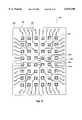
- FIG. 9is a top plan view of routing traces utilized as deactivation mechanisms according to the present invention.
- FIG. 10is a side cross-sectional view of a prior art pinched resistor pair
- FIG. 11is a side cross-sectional view of a prior art metallization structure.
- FIG. 12is a top plan view of the prior art metallization structure of FIG. 10.
- FIGS. 1-9illustrate various trace configurations on a contact surface of a semiconductor device according to the present invention. It should be understood that the illustrations are not meant to be actual views of any particular semiconductor IC device, but are merely idealized representations which are employed to more clearly and fully depict the present invention than would otherwise be possible. Additionally, elements and features common to FIGS. 1-9 retain the same numerical designation.
- FIG. 1shows a top plan view of an active surface 102 for a flip-chip 100.
- the active surface 102includes a plurality of ball or bump sites 104 upon which minute solder balls or other conductive material elements (not shown) are to be disposed.
- the ball or bump sites 104are patterned in specific locations for active surface-down mounting to contact sites of metal conductors of a carrier substrate (not shown), such as a printed circuit board, wherein the contact sites are a mirror-image of the ball or bump sites 104 pattern on the flip-chip 100.
- the ball or bump sites 104are in electrical communication with external communication traces 106 which are used to route power to and signals to and from the flip-chip 100 integrated circuitry (not shown--i.e., below the active surface 102). It is, of course, understood that although the ball or bump sites 104 are illustrated as substantially square, they may be of any shape, including round, as shown as round ball site 108.
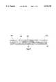
- FIG. 2shows a side cross-sectional view along line 2--2 of FIG. 1 which shows a contact 112 making an electrical connection between the external communication trace 106 and an internal trace 114 within the flip-chip 100.
- FIG. 1shows all of the external communication traces 106 routing from contacts 112 (see FIG. 2) which are about peripheral edges 116 of the flip-chip 100, it is understood that each contact 112 (see FIG. 2) could be positioned anywhere to extend through to the active surface 102 of the flip-chip 100.
- FIG. 3illustrates three such routing traces: a first routing trace 122, a second routing trace 124, and a third routing trace 126.
- the routing tracee.g., 122, 124, and 126
- the routing tracecan be considerably smaller (thinner in width and/or height) than the external communication traces 106, since the routing traces generally require substantially less current than the external communication traces 106.
- External communication traces 106route power to and signals to and from an external device (not shown) which, for output signals, requires amplifying the original signal within the semiconductor device to a sufficiently strong signal for external communication.
- the ball or bump sites 104, the external communication traces 106, and the routing traces 122, 124, and 126may be formed in separate steps or simultaneously formed by various methods, including, but not limited to:
- the first routing trace 122is an example of a short "jumping" trace.
- the path for connecting first internal trace 132 with second internal trace 134is blocked by a lateral trace 136 which is running perpendicular to the plane of the cross-section on a fourth level 138 of the multilevel structure of the flip-chip 100.
- a first internal trace-to-first trace contact 142is formed to connect the first internal trace 132 with the first routing trace 122 and a first trace-to-second internal trace contact 144 is formed to connect the first routing trace 122 with the second internal trace 134, thereby "jumping" the lateral trace 136.
- the second routing trace 124extends substantially the length of the flip-chip 100.
- Such a routing traceis very advantageous for components in electrical communication with one another, but which are widely spaced from one another. If such a routing trace were not available, the components could be connected internally, which would likely require a lengthy, serpentine route shifting from layer to layer in the multilayer structure of the flip-chip 100.
- the direct route of the second routing trace 124greatly reduces the overall length of the trace, thereby decreasing the time required for signals to travel between the components, and reduces the capacitance due to a reduction of the amount of metal required.
- the third routing trace 126(FIG. 3) illustrates that the routing traces can be patterned to "snake" around the ball or bump sites 104 and external communication traces 106.
- FIG. 5illustrates a first semiconductor die 152 and a second semiconductor die 154 placed in separate recesses in a semiconductor carrier 156.
- the semiconductor carrier 156can be made of silicon, ceramic material, or even metal with a surface of insulative material etched to form recesses having sloped walls.
- the semiconductor carrier 156should have a coefficient of thermal expansion (CTE) which is similar to the CTE of the semiconductor dice and filler, so that the heat expansion and contraction does not break the routing traces.
- CTEcoefficient of thermal expansion
- the first semiconductor die 152 and the second semiconductor die 154are substantially flush with a top surface 160 of the semiconductor carrier 156.
- An appropriate filler material 158such as "filled" epoxies or silicones, is utilized to fill any gaps in the recess.
- the filler material 158is preferably planarized to be substantially flush with the first and second semiconductor dice 152 and 154, and the semiconductor carrier top surface 160. However, if the filler material 158 is planarized, the ball or bump sites, the external communication traces, and the routing traces must be formed thereafter. With such a configuration, routing traces 162 can be patterned to interconnect the first and second semiconductor dice 152 and 154.
- FIG. 7illustrates the first semiconductor die 152 and a second semiconductor die 154 placed in a single recess in a semiconductor carrier 156, wherein the first semiconductor die 152 and the second semiconductor die 154 abut one another.
- FIG. 8(a cross-sectional view of FIG. 7 along line 8--8), the first semiconductor die 152 and the second semiconductor die 154 are substantially flush with a top surface 160 of the semiconductor carrier 156.
- An appropriate filler material 158is utilized to fill any gaps in the recess.
- the filler material 158is usually planarized to be substantially flush with the first and second semiconductor dice 152 and 154, and the semiconductor carrier top surface 160.
- routing traces 162can be patterned to interconnect the first and second semiconductor dice 152 and 154.
- An insulative spacer(not shown) may be disposed between the first and second semiconductor dice 152 and 154 to prevent shorting therebetween.
- FIGS. 5-8considerably simplify inter-semiconductor dice communication.
- a signal from the first semiconductor diewould have to be amplified and sent from an interconnection out of the first semiconductor die and through a external communication trace to a bond pad.
- the bond padwould be connected to a carrier substrate, such as a printed circuit board, FR4, or the like, with a solder ball, conductive epoxy pillar, or the like.
- the carrier substratewould, in turn, route the signal through a trace to a solder ball connected to a bond pad on a second semiconductor device. The signal would then be directed by an external communication trace to an interconnection into the second semiconductor device.
- This embodimentreduces or may eliminate any requirement for signal amplification and the necessity of using the valuable space which would be required by the additional external communication traces and bond pads on both the first and second semiconductor dice, as well as the additional trace on the external carrier substrate. Furthermore, this embodiment allows for faster transmission of signals between the two semiconductor dice and reduces capacitance by reducing the amount of metal required to form the connections. This embodiment also eliminates the use of an interposer board with yet another set of solder balls to a higher level carrier.
- Yet another embodiment of the present inventioncomprises using routing traces as repair mechanisms.
- a series of traces 172a-dcan be used as deactivation mechanisms on a semiconductor device 170.
- a traceshown as trace 172d
- this deactivationwill result in the activation of a redundant circuit to take over for the defective circuit.
- this deactivation of a defective portion of a semiconductor devicewill simply deactivate the defective portion of the semiconductor device. For example, in a memory chip, this deactivation will result in isolation of defective storage capacity on the memory chip.
- Prior art fusesare programming devices which are blown by a tester to isolate area on a chip. However, blowing these fuses can cause damage to the chip.
- the repair mechanisms shown in FIG. 9function to isolate a short or a latched-up area without risking damage to the chip.
Landscapes
- Physics & Mathematics (AREA)
- Condensed Matter Physics & Semiconductors (AREA)
- General Physics & Mathematics (AREA)
- Engineering & Computer Science (AREA)
- Computer Hardware Design (AREA)
- Microelectronics & Electronic Packaging (AREA)
- Power Engineering (AREA)
- Semiconductor Integrated Circuits (AREA)
- Wire Bonding (AREA)
Abstract
Description
Claims (6)
Priority Applications (6)
| Application Number | Priority Date | Filing Date | Title |
|---|---|---|---|
| US09/229,373US6078100A (en) | 1999-01-13 | 1999-01-13 | Utilization of die repattern layers for die internal connections |
| US09/287,456US6124195A (en) | 1999-01-13 | 1999-04-07 | Utilization of die repattern layers for die internal connections |
| US09/599,752US6331736B1 (en) | 1999-01-13 | 2000-06-22 | Utilization of die repattern layers for die internal connections |
| US09/917,130US6541850B2 (en) | 1999-01-13 | 2001-07-27 | Utilization of die active surfaces for laterally extending die internal and external connections |
| US10/173,935US6673707B2 (en) | 1999-01-13 | 2002-06-17 | Method of forming semiconductor device utilizing die active surfaces for laterally extending die internal and external connections |
| US10/345,895US6664632B2 (en) | 1999-01-13 | 2003-01-15 | Utilization of die active surfaces for laterally extending die internal and external connections |
Applications Claiming Priority (1)
| Application Number | Priority Date | Filing Date | Title |
|---|---|---|---|
| US09/229,373US6078100A (en) | 1999-01-13 | 1999-01-13 | Utilization of die repattern layers for die internal connections |
Related Child Applications (1)
| Application Number | Title | Priority Date | Filing Date |
|---|---|---|---|
| US09/287,456DivisionUS6124195A (en) | 1999-01-13 | 1999-04-07 | Utilization of die repattern layers for die internal connections |
Publications (1)
| Publication Number | Publication Date |
|---|---|
| US6078100Atrue US6078100A (en) | 2000-06-20 |
Family
ID=22860944
Family Applications (6)
| Application Number | Title | Priority Date | Filing Date |
|---|---|---|---|
| US09/229,373Expired - LifetimeUS6078100A (en) | 1999-01-13 | 1999-01-13 | Utilization of die repattern layers for die internal connections |
| US09/287,456Expired - LifetimeUS6124195A (en) | 1999-01-13 | 1999-04-07 | Utilization of die repattern layers for die internal connections |
| US09/599,752Expired - Fee RelatedUS6331736B1 (en) | 1999-01-13 | 2000-06-22 | Utilization of die repattern layers for die internal connections |
| US09/917,130Expired - LifetimeUS6541850B2 (en) | 1999-01-13 | 2001-07-27 | Utilization of die active surfaces for laterally extending die internal and external connections |
| US10/173,935Expired - LifetimeUS6673707B2 (en) | 1999-01-13 | 2002-06-17 | Method of forming semiconductor device utilizing die active surfaces for laterally extending die internal and external connections |
| US10/345,895Expired - LifetimeUS6664632B2 (en) | 1999-01-13 | 2003-01-15 | Utilization of die active surfaces for laterally extending die internal and external connections |
Family Applications After (5)
| Application Number | Title | Priority Date | Filing Date |
|---|---|---|---|
| US09/287,456Expired - LifetimeUS6124195A (en) | 1999-01-13 | 1999-04-07 | Utilization of die repattern layers for die internal connections |
| US09/599,752Expired - Fee RelatedUS6331736B1 (en) | 1999-01-13 | 2000-06-22 | Utilization of die repattern layers for die internal connections |
| US09/917,130Expired - LifetimeUS6541850B2 (en) | 1999-01-13 | 2001-07-27 | Utilization of die active surfaces for laterally extending die internal and external connections |
| US10/173,935Expired - LifetimeUS6673707B2 (en) | 1999-01-13 | 2002-06-17 | Method of forming semiconductor device utilizing die active surfaces for laterally extending die internal and external connections |
| US10/345,895Expired - LifetimeUS6664632B2 (en) | 1999-01-13 | 2003-01-15 | Utilization of die active surfaces for laterally extending die internal and external connections |
Country Status (1)
| Country | Link |
|---|---|
| US (6) | US6078100A (en) |
Cited By (18)
| Publication number | Priority date | Publication date | Assignee | Title |
|---|---|---|---|---|
| US6303977B1 (en)* | 1998-12-03 | 2001-10-16 | Texas Instruments Incorporated | Fully hermetic semiconductor chip, including sealed edge sides |
| US6307268B1 (en)* | 1999-12-30 | 2001-10-23 | Winbond Electronics Corp | Suppression of interconnect stress migration by refractory metal plug |
| US6331736B1 (en)* | 1999-01-13 | 2001-12-18 | Micron Technology, Inc. | Utilization of die repattern layers for die internal connections |
| US20020036354A1 (en)* | 2000-09-28 | 2002-03-28 | Akira Yamaguchi | Semiconductor device |
| US6528887B2 (en) | 2000-04-10 | 2003-03-04 | Onix Microsystems | Conductive equipotential landing pads formed on the underside of a MEMS device |
| US6608377B2 (en) | 2001-01-30 | 2003-08-19 | Samsung Electronics Co., Ltd. | Wafer level package including ground metal layer |
| US6630735B1 (en)* | 1999-04-09 | 2003-10-07 | Digirad Corporation | Insulator/metal bonding island for active-area silver epoxy bonding |
| US20030205814A1 (en)* | 1999-03-19 | 2003-11-06 | Kabushiki Kaisha Toshiba | Wiring structure of semiconductor device |
| US6674174B2 (en)* | 2001-11-13 | 2004-01-06 | Skyworks Solutions, Inc. | Controlled impedance transmission lines in a redistribution layer |
| US6710454B1 (en) | 2000-02-16 | 2004-03-23 | Micron Technology, Inc. | Adhesive layer for an electronic apparatus having multiple semiconductor devices |
| US20040084768A1 (en)* | 2002-04-02 | 2004-05-06 | Devnani Nurwati S. | Integrated circuit and method of manufacturing an integrated circuit and package |
| US6991970B2 (en) | 2001-08-30 | 2006-01-31 | Micron Technology, Inc. | Method and apparatus for circuit completion through the use of ball bonds or other connections during the formation of semiconductor device |
| US20060049826A1 (en)* | 2001-03-01 | 2006-03-09 | Onix Microsystems | Optical cross-connect system |
| US20060051707A1 (en)* | 2004-09-09 | 2006-03-09 | Rebecca Shia | Conductive lithographic polymer and method of making devices using same |
| US7064447B2 (en)* | 2001-08-10 | 2006-06-20 | Micron Technology, Inc. | Bond pad structure comprising multiple bond pads with metal overlap |
| US7064450B1 (en)* | 2004-05-11 | 2006-06-20 | Xilinx, Inc. | Semiconductor die with high density offset-inline bond arrangement |
| EP1837910A1 (en)* | 2006-03-21 | 2007-09-26 | Stmicroelectronics Sa | Integrated-circuit chip with offset external contacts and method of manufacturing such a chip. |
| US20120263868A1 (en)* | 2004-11-09 | 2012-10-18 | Taiwan Semiconductor Manufacturing Company, Ltd. | Interconnect Structure to Reduce Stress Induced Voiding Effect |
Families Citing this family (21)
| Publication number | Priority date | Publication date | Assignee | Title |
|---|---|---|---|---|
| US6740573B2 (en)* | 1995-02-17 | 2004-05-25 | Micron Technology, Inc. | Method for forming an integrated circuit interconnect using a dual poly process |
| US6329712B1 (en) | 1998-03-25 | 2001-12-11 | Micron Technology, Inc. | High density flip chip memory arrays |
| JP3549017B2 (en)* | 2000-07-21 | 2004-08-04 | 松下電器産業株式会社 | Flip chip mounting method |
| DE10152317A1 (en)* | 2001-10-26 | 2003-05-08 | Bayer Ag | Mineral-reinforced impact-modified polycarbonate blends |
| US6617181B1 (en)* | 2002-02-01 | 2003-09-09 | Lsi Logic Corporation | Flip chip testing |
| US6559544B1 (en)* | 2002-03-28 | 2003-05-06 | Alan Roth | Programmable interconnect for semiconductor devices |
| US6680530B1 (en)* | 2002-08-12 | 2004-01-20 | International Business Machines Corporation | Multi-step transmission line for multilayer packaging |
| US6798069B1 (en)* | 2003-03-28 | 2004-09-28 | Lsi Logic Corporation | Integrated circuit having adaptable core and input/output regions with multi-layer pad trace conductors |
| US7620915B2 (en)* | 2004-02-13 | 2009-11-17 | Ludwig Lester F | Electronic document editing employing multiple cursors |
| US20050285222A1 (en) | 2004-06-29 | 2005-12-29 | Kong-Beng Thei | New fuse structure |
| US20060163734A1 (en)* | 2005-01-24 | 2006-07-27 | Taiwan Semiconductor Manufacturing Company, Ltd. | Fuse structure and method for making the same |
| US20060244156A1 (en)* | 2005-04-18 | 2006-11-02 | Tao Cheng | Bond pad structures and semiconductor devices using the same |
| JP4779485B2 (en)* | 2005-07-22 | 2011-09-28 | ブラザー工業株式会社 | Substrate sheet and circuit board manufacturing method |
| FR2910703B1 (en)* | 2006-12-22 | 2009-03-20 | St Microelectronics Sa | IMAGEUR DEVICE HAVING A LAST LEVEL OF COPPER-ALUMINUM INTERCONNECTION |
| WO2008155085A1 (en)* | 2007-06-18 | 2008-12-24 | Microgan Gmbh | Electric circuit with vertical contacts |
| US7777339B2 (en)* | 2007-07-30 | 2010-08-17 | International Business Machines Corporation | Semiconductor chips with reduced stress from underfill at edge of chip |
| US8946873B2 (en) | 2007-08-28 | 2015-02-03 | Micron Technology, Inc. | Redistribution structures for microfeature workpieces |
| US7956466B2 (en) | 2008-05-09 | 2011-06-07 | International Business Machines Corporation | Structure for interconnect structure containing various capping materials for electrical fuse and other related applications |
| US8772156B2 (en)* | 2008-05-09 | 2014-07-08 | International Business Machines Corporation | Methods of fabricating interconnect structures containing various capping materials for electrical fuse and other related applications |
| US9929114B1 (en)* | 2016-11-02 | 2018-03-27 | Vanguard International Semiconductor Corporation | Bonding pad structure having island portions and method for manufacturing the same |
| US10295588B2 (en) | 2016-12-22 | 2019-05-21 | Xcelsis Corporation | Wafer testing without direct probing |
Citations (6)
| Publication number | Priority date | Publication date | Assignee | Title |
|---|---|---|---|---|
| US3461357A (en)* | 1967-09-15 | 1969-08-12 | Ibm | Multilevel terminal metallurgy for semiconductor devices |
| US3809625A (en)* | 1972-08-15 | 1974-05-07 | Gen Motors Corp | Method of making contact bumps on flip-chips |
| US3881971A (en)* | 1972-11-29 | 1975-05-06 | Ibm | Method for fabricating aluminum interconnection metallurgy system for silicon devices |
| US5523626A (en)* | 1993-09-08 | 1996-06-04 | Nec Corporation | Semiconductor device and fabrication process therefor |
| US5534465A (en)* | 1995-01-10 | 1996-07-09 | At&T Corp. | Method for making multichip circuits using active semiconductor substrates |
| US5904556A (en)* | 1995-01-11 | 1999-05-18 | Hitachi, Ltd. | Method for making semiconductor integrated circuit device having interconnection structure using tungsten film |
Family Cites Families (35)
| Publication number | Priority date | Publication date | Assignee | Title |
|---|---|---|---|---|
| US4808552A (en)* | 1985-09-11 | 1989-02-28 | Texas Instruments Incorporated | Process for making vertically-oriented interconnections for VLSI devices |
| US4988423A (en)* | 1987-06-19 | 1991-01-29 | Matsushita Electric Industrial Co., Ltd. | Method for fabricating interconnection structure |
| JPH01253263A (en)* | 1988-04-01 | 1989-10-09 | Stanley Electric Co Ltd | How to manufacture fuse diodes |
| US5106461A (en)* | 1989-04-04 | 1992-04-21 | Massachusetts Institute Of Technology | High-density, multi-level interconnects, flex circuits, and tape for tab |
| US5400262A (en)* | 1989-09-20 | 1995-03-21 | Aptix Corporation | Universal interconnect matrix array |
| US5231590A (en)* | 1989-10-13 | 1993-07-27 | Zilog, Inc. | Technique for modifying an integrated circuit layout |
| US5224022A (en)* | 1990-05-15 | 1993-06-29 | Microelectronics And Computer Technology Corporation | Reroute strategy for high density substrates |
| DE69133311T2 (en)* | 1990-10-15 | 2004-06-24 | Aptix Corp., San Jose | Connection substrate with integrated circuit for programmable connection and sample analysis |
| US5130768A (en)* | 1990-12-07 | 1992-07-14 | Digital Equipment Corporation | Compact, high-density packaging apparatus for high performance semiconductor devices |
| US5261155A (en) | 1991-08-12 | 1993-11-16 | International Business Machines Corporation | Method for bonding flexible circuit to circuitized substrate to provide electrical connection therebetween using different solders |
| US5341310A (en)* | 1991-12-17 | 1994-08-23 | International Business Machines Corporation | Wiring layout design method and system for integrated circuits |
| US5282312A (en)* | 1991-12-31 | 1994-02-01 | Tessera, Inc. | Multi-layer circuit construction methods with customization features |
| US5329323A (en) | 1992-03-25 | 1994-07-12 | Kevin Biles | Apparatus and method for producing 3-dimensional images |
| US5414637A (en)* | 1992-06-24 | 1995-05-09 | International Business Machines Corporation | Intra-module spare routing for high density electronic packages |
| US5244837A (en)* | 1993-03-19 | 1993-09-14 | Micron Semiconductor, Inc. | Semiconductor electrical interconnection methods |
| US5329423A (en)* | 1993-04-13 | 1994-07-12 | Scholz Kenneth D | Compressive bump-and-socket interconnection scheme for integrated circuits |
| US5495397A (en)* | 1993-04-27 | 1996-02-27 | International Business Machines Corporation | Three dimensional package and architecture for high performance computer |
| US5572409A (en)* | 1994-02-08 | 1996-11-05 | Prolinx Labs Corporation | Apparatus including a programmable socket adapter for coupling an electronic component to a component socket on a printed circuit board |
| WO1995025341A1 (en)* | 1994-03-15 | 1995-09-21 | Irvine Sensors Corporation | 3d stack of ic chips having leads reached by vias through passivation covering access plane |
| US5420455A (en)* | 1994-03-31 | 1995-05-30 | International Business Machines Corp. | Array fuse damage protection devices and fabrication method |
| US5571751A (en)* | 1994-05-09 | 1996-11-05 | National Semiconductor Corporation | Interconnect structures for integrated circuits |
| US5632631A (en)* | 1994-06-07 | 1997-05-27 | Tessera, Inc. | Microelectronic contacts with asperities and methods of making same |
| US5698895A (en)* | 1994-06-23 | 1997-12-16 | Cubic Memory, Inc. | Silicon segment programming method and apparatus |
| US5506172A (en)* | 1994-08-29 | 1996-04-09 | Micron Technology, Inc. | Semiconductor processing method of forming an electrical interconnection between an outer layer and an inner layer |
| US5491302A (en)* | 1994-09-19 | 1996-02-13 | Tessera, Inc. | Microelectronic bonding with lead motion |
| US5661330A (en)* | 1995-03-14 | 1997-08-26 | International Business Machines Corporation | Fabrication, testing and repair of multichip semiconductor structures having connect assemblies with fuses |
| TW310470B (en)* | 1995-05-01 | 1997-07-11 | Micron Technology Inc | |
| US5597470A (en)* | 1995-06-18 | 1997-01-28 | Tessera, Inc. | Method for making a flexible lead for a microelectronic device |
| JP2825083B2 (en) | 1996-08-20 | 1998-11-18 | 日本電気株式会社 | Semiconductor element mounting structure |
| US6175161B1 (en)* | 1998-05-22 | 2001-01-16 | Alpine Microsystems, Inc. | System and method for packaging integrated circuits |
| US5898223A (en) | 1997-10-08 | 1999-04-27 | Lucent Technologies Inc. | Chip-on-chip IC packages |
| US6075712A (en) | 1999-01-08 | 2000-06-13 | Intel Corporation | Flip-chip having electrical contact pads on the backside of the chip |
| US6078100A (en)* | 1999-01-13 | 2000-06-20 | Micron Technology, Inc. | Utilization of die repattern layers for die internal connections |
| US6181569B1 (en) | 1999-06-07 | 2001-01-30 | Kishore K. Chakravorty | Low cost chip size package and method of fabricating the same |
| US6388335B1 (en) | 1999-12-14 | 2002-05-14 | Atmel Corporation | Integrated circuit package formed at a wafer level |
- 1999
- 1999-01-13USUS09/229,373patent/US6078100A/ennot_activeExpired - Lifetime
- 1999-04-07USUS09/287,456patent/US6124195A/ennot_activeExpired - Lifetime
- 2000
- 2000-06-22USUS09/599,752patent/US6331736B1/ennot_activeExpired - Fee Related
- 2001
- 2001-07-27USUS09/917,130patent/US6541850B2/ennot_activeExpired - Lifetime
- 2002
- 2002-06-17USUS10/173,935patent/US6673707B2/ennot_activeExpired - Lifetime
- 2003
- 2003-01-15USUS10/345,895patent/US6664632B2/ennot_activeExpired - Lifetime
Patent Citations (6)
| Publication number | Priority date | Publication date | Assignee | Title |
|---|---|---|---|---|
| US3461357A (en)* | 1967-09-15 | 1969-08-12 | Ibm | Multilevel terminal metallurgy for semiconductor devices |
| US3809625A (en)* | 1972-08-15 | 1974-05-07 | Gen Motors Corp | Method of making contact bumps on flip-chips |
| US3881971A (en)* | 1972-11-29 | 1975-05-06 | Ibm | Method for fabricating aluminum interconnection metallurgy system for silicon devices |
| US5523626A (en)* | 1993-09-08 | 1996-06-04 | Nec Corporation | Semiconductor device and fabrication process therefor |
| US5534465A (en)* | 1995-01-10 | 1996-07-09 | At&T Corp. | Method for making multichip circuits using active semiconductor substrates |
| US5904556A (en)* | 1995-01-11 | 1999-05-18 | Hitachi, Ltd. | Method for making semiconductor integrated circuit device having interconnection structure using tungsten film |
Cited By (46)
| Publication number | Priority date | Publication date | Assignee | Title |
|---|---|---|---|---|
| US6303977B1 (en)* | 1998-12-03 | 2001-10-16 | Texas Instruments Incorporated | Fully hermetic semiconductor chip, including sealed edge sides |
| US6331736B1 (en)* | 1999-01-13 | 2001-12-18 | Micron Technology, Inc. | Utilization of die repattern layers for die internal connections |
| US6673707B2 (en) | 1999-01-13 | 2004-01-06 | Micron Technology, Inc. | Method of forming semiconductor device utilizing die active surfaces for laterally extending die internal and external connections |
| US6541850B2 (en)* | 1999-01-13 | 2003-04-01 | Micron Technology, Inc. | Utilization of die active surfaces for laterally extending die internal and external connections |
| US6664632B2 (en) | 1999-01-13 | 2003-12-16 | Micron Technologies, Inc. | Utilization of die active surfaces for laterally extending die internal and external connections |
| US20030205814A1 (en)* | 1999-03-19 | 2003-11-06 | Kabushiki Kaisha Toshiba | Wiring structure of semiconductor device |
| US6864583B2 (en)* | 1999-03-19 | 2005-03-08 | Kabushiki Kaisha Toshiba | Wiring structure of semiconductor device |
| US6630735B1 (en)* | 1999-04-09 | 2003-10-07 | Digirad Corporation | Insulator/metal bonding island for active-area silver epoxy bonding |
| US6307268B1 (en)* | 1999-12-30 | 2001-10-23 | Winbond Electronics Corp | Suppression of interconnect stress migration by refractory metal plug |
| US20040113246A1 (en)* | 2000-02-16 | 2004-06-17 | Micron Technology, Inc. | Method of packaging at a wafer level |
| US20060258052A1 (en)* | 2000-02-16 | 2006-11-16 | Micron Technology, Inc. | Wafer level pre-packaged flip chip |
| US20060261475A1 (en)* | 2000-02-16 | 2006-11-23 | Micron Technology, Inc. | Wafer level pre-packaged flip chip |
| US7812447B2 (en) | 2000-02-16 | 2010-10-12 | Micron Technology, Inc. | Wafer level pre-packaged flip chip |
| US6710454B1 (en) | 2000-02-16 | 2004-03-23 | Micron Technology, Inc. | Adhesive layer for an electronic apparatus having multiple semiconductor devices |
| US7943422B2 (en) | 2000-02-16 | 2011-05-17 | Micron Technology, Inc. | Wafer level pre-packaged flip chip |
| US20040104486A1 (en)* | 2000-02-16 | 2004-06-03 | Micron Technology, Inc. | Electronic apparatus having an adhesive layer from wafer level packaging |
| US7808112B2 (en) | 2000-02-16 | 2010-10-05 | Micron Technology, Inc. | Wafer level pre-packaged flip chip system |
| US20060261493A1 (en)* | 2000-02-16 | 2006-11-23 | Micron Technology, Inc. | Wafer level pre-packaged flip chip systems |
| US20060255475A1 (en)* | 2000-02-16 | 2006-11-16 | Micron Technology, Inc. | Wafer level pre-packaged flip chip system |
| US7646102B2 (en) | 2000-02-16 | 2010-01-12 | Micron Technology, Inc. | Wafer level pre-packaged flip chip systems |
| US6586841B1 (en)* | 2000-02-23 | 2003-07-01 | Onix Microsystems, Inc. | Mechanical landing pad formed on the underside of a MEMS device |
| US6764936B2 (en) | 2000-04-10 | 2004-07-20 | Onix Microsystems, Inc. | Mechanical landing pad formed on the underside of a MEMS device |
| US6528887B2 (en) | 2000-04-10 | 2003-03-04 | Onix Microsystems | Conductive equipotential landing pads formed on the underside of a MEMS device |
| US20020036354A1 (en)* | 2000-09-28 | 2002-03-28 | Akira Yamaguchi | Semiconductor device |
| US6888254B2 (en)* | 2000-09-28 | 2005-05-03 | Kabushiki Kaisha Toshiba | Semiconductor device |
| US6608377B2 (en) | 2001-01-30 | 2003-08-19 | Samsung Electronics Co., Ltd. | Wafer level package including ground metal layer |
| US20060049826A1 (en)* | 2001-03-01 | 2006-03-09 | Onix Microsystems | Optical cross-connect system |
| US7183633B2 (en) | 2001-03-01 | 2007-02-27 | Analog Devices Inc. | Optical cross-connect system |
| US7064447B2 (en)* | 2001-08-10 | 2006-06-20 | Micron Technology, Inc. | Bond pad structure comprising multiple bond pads with metal overlap |
| US7146722B2 (en) | 2001-08-10 | 2006-12-12 | Micron Technology, Inc. | Method of forming a bond pad structure |
| US20060121650A1 (en)* | 2001-08-30 | 2006-06-08 | Rich Fogal | Method and apparatus for circuit completion through the use of ball bonds or other connections during the formation of a semiconductor device |
| US6991970B2 (en) | 2001-08-30 | 2006-01-31 | Micron Technology, Inc. | Method and apparatus for circuit completion through the use of ball bonds or other connections during the formation of semiconductor device |
| US6674174B2 (en)* | 2001-11-13 | 2004-01-06 | Skyworks Solutions, Inc. | Controlled impedance transmission lines in a redistribution layer |
| US20040084768A1 (en)* | 2002-04-02 | 2004-05-06 | Devnani Nurwati S. | Integrated circuit and method of manufacturing an integrated circuit and package |
| US7001834B2 (en)* | 2002-04-02 | 2006-02-21 | Agilent Technologies, Inc. | Integrated circuit and method of manufacturing an integrated circuit and package |
| US7064450B1 (en)* | 2004-05-11 | 2006-06-20 | Xilinx, Inc. | Semiconductor die with high density offset-inline bond arrangement |
| US20070269743A1 (en)* | 2004-09-09 | 2007-11-22 | Rebecca Shia | Conductive lithographic polymer and method of making devices using same |
| US7700246B2 (en) | 2004-09-09 | 2010-04-20 | Intel Corporation | Conductive lithographic polymer and method of making devices using same |
| US20060051707A1 (en)* | 2004-09-09 | 2006-03-09 | Rebecca Shia | Conductive lithographic polymer and method of making devices using same |
| US7279268B2 (en)* | 2004-09-09 | 2007-10-09 | Intel Corporation | Conductive lithographic polymer and method of making devices using same |
| US20120263868A1 (en)* | 2004-11-09 | 2012-10-18 | Taiwan Semiconductor Manufacturing Company, Ltd. | Interconnect Structure to Reduce Stress Induced Voiding Effect |
| US8513115B2 (en)* | 2004-11-09 | 2013-08-20 | Taiwan Semiconductor Manufacturing Company, Ltd. | Method of forming an interconnect structure having an enlarged region |
| US8785323B2 (en) | 2004-11-09 | 2014-07-22 | Taiwan Semiconductor Manufacturing Company, Ltd. | Method of forming an interconnect structure having an enlarged region |
| EP1837910A1 (en)* | 2006-03-21 | 2007-09-26 | Stmicroelectronics Sa | Integrated-circuit chip with offset external contacts and method of manufacturing such a chip. |
| US7701047B2 (en) | 2006-03-21 | 2010-04-20 | Stmicroelectronics S.A. | Integrated-circuit chip with offset external pads and method for fabricating such a chip |
| US20070228508A1 (en)* | 2006-03-21 | 2007-10-04 | Stmicroelectronics S.A. | Integrated-circuit chip with offset external pads and method for fabricating such a chip |
Also Published As
| Publication number | Publication date |
|---|---|
| US6541850B2 (en) | 2003-04-01 |
| US6331736B1 (en) | 2001-12-18 |
| US6664632B2 (en) | 2003-12-16 |
| US20020027278A1 (en) | 2002-03-07 |
| US6673707B2 (en) | 2004-01-06 |
| US20030127662A1 (en) | 2003-07-10 |
| US20020158321A1 (en) | 2002-10-31 |
| US6124195A (en) | 2000-09-26 |
Similar Documents
| Publication | Publication Date | Title |
|---|---|---|
| US6078100A (en) | Utilization of die repattern layers for die internal connections | |
| US7002248B2 (en) | Semiconductor components having multiple on board capacitors | |
| US7183658B2 (en) | Low cost microelectronic circuit package | |
| US7355273B2 (en) | Semiconductor dice having back side redistribution layer accessed using through-silicon vias, methods | |
| EP0622847A2 (en) | Three dimensional package and architecture for high performance computer | |
| US7335995B2 (en) | Microelectronic assembly having array including passive elements and interconnects | |
| EP3547364B1 (en) | Semiconductor chip and semiconductor package including the same | |
| US6359234B1 (en) | Package substrate for mounting semiconductor chip with low impedance and semiconductor device having the same | |
| US6441486B1 (en) | BGA substrate via structure | |
| JP2001274288A (en) | Integrated circuit chip carrier structure | |
| US6437436B2 (en) | Integrated circuit chip package with test points | |
| US20060055018A1 (en) | Semiconductor device | |
| US5640308A (en) | Field programmable circuit module | |
| US20080043447A1 (en) | Semiconductor package having laser-embedded terminals | |
| US7026718B1 (en) | Stacked multi-component integrated circuit microprocessor | |
| US20250006682A1 (en) | Semiconductor packages with multiple types of solder balls | |
| KR100633495B1 (en) | Selective connection in ic packaging | |
| US7884465B2 (en) | Semiconductor package with passive elements embedded within a semiconductor chip | |
| KR100866137B1 (en) | Stack package | |
| CN215220719U (en) | Double-sided packaging structure | |
| KR100712517B1 (en) | Interposer of Semiconductor Device with Air Gap Structure | |
| JP2002270723A (en) | Semiconductor device, semiconductor chip and mounting substrate | |
| US6188133B1 (en) | Semiconductor with plurality of connecting parts arranged on lower surface of a substrate | |
| KR100256306B1 (en) | Stacked Multi-Chip Modules | |
| CN112670259A (en) | Wafer packaging element |
Legal Events
| Date | Code | Title | Description |
|---|---|---|---|
| AS | Assignment | Owner name:MICRON TECHNOLOGY, INC., IDAHO Free format text:ASSIGNMENT OF ASSIGNORS INTEREST;ASSIGNORS:DUESMAN, KEVIN G.;FARNWORTH, WARREN;REEL/FRAME:010205/0241 Effective date:19990106 | |
| STCF | Information on status: patent grant | Free format text:PATENTED CASE | |
| FEPP | Fee payment procedure | Free format text:PAYOR NUMBER ASSIGNED (ORIGINAL EVENT CODE: ASPN); ENTITY STATUS OF PATENT OWNER: LARGE ENTITY | |
| AS | Assignment | Owner name:CHASE MANHATTAN BANK, AS COLLATERAL AGENT, THE, NE Free format text:SECURITY INTEREST;ASSIGNOR:MASCOTECH, INC.;REEL/FRAME:011457/0321 Effective date:20001128 | |
| FPAY | Fee payment | Year of fee payment:4 | |
| FPAY | Fee payment | Year of fee payment:8 | |
| CC | Certificate of correction | ||
| FPAY | Fee payment | Year of fee payment:12 | |
| AS | Assignment | Owner name:U.S. BANK NATIONAL ASSOCIATION, AS COLLATERAL AGENT, CALIFORNIA Free format text:SECURITY INTEREST;ASSIGNOR:MICRON TECHNOLOGY, INC.;REEL/FRAME:038669/0001 Effective date:20160426 Owner name:U.S. BANK NATIONAL ASSOCIATION, AS COLLATERAL AGEN Free format text:SECURITY INTEREST;ASSIGNOR:MICRON TECHNOLOGY, INC.;REEL/FRAME:038669/0001 Effective date:20160426 | |
| AS | Assignment | Owner name:MORGAN STANLEY SENIOR FUNDING, INC., AS COLLATERAL AGENT, MARYLAND Free format text:PATENT SECURITY AGREEMENT;ASSIGNOR:MICRON TECHNOLOGY, INC.;REEL/FRAME:038954/0001 Effective date:20160426 Owner name:MORGAN STANLEY SENIOR FUNDING, INC., AS COLLATERAL Free format text:PATENT SECURITY AGREEMENT;ASSIGNOR:MICRON TECHNOLOGY, INC.;REEL/FRAME:038954/0001 Effective date:20160426 | |
| AS | Assignment | Owner name:U.S. BANK NATIONAL ASSOCIATION, AS COLLATERAL AGENT, CALIFORNIA Free format text:CORRECTIVE ASSIGNMENT TO CORRECT THE REPLACE ERRONEOUSLY FILED PATENT #7358718 WITH THE CORRECT PATENT #7358178 PREVIOUSLY RECORDED ON REEL 038669 FRAME 0001. ASSIGNOR(S) HEREBY CONFIRMS THE SECURITY INTEREST;ASSIGNOR:MICRON TECHNOLOGY, INC.;REEL/FRAME:043079/0001 Effective date:20160426 Owner name:U.S. BANK NATIONAL ASSOCIATION, AS COLLATERAL AGEN Free format text:CORRECTIVE ASSIGNMENT TO CORRECT THE REPLACE ERRONEOUSLY FILED PATENT #7358718 WITH THE CORRECT PATENT #7358178 PREVIOUSLY RECORDED ON REEL 038669 FRAME 0001. ASSIGNOR(S) HEREBY CONFIRMS THE SECURITY INTEREST;ASSIGNOR:MICRON TECHNOLOGY, INC.;REEL/FRAME:043079/0001 Effective date:20160426 | |
| AS | Assignment | Owner name:JPMORGAN CHASE BANK, N.A., AS COLLATERAL AGENT, ILLINOIS Free format text:SECURITY INTEREST;ASSIGNORS:MICRON TECHNOLOGY, INC.;MICRON SEMICONDUCTOR PRODUCTS, INC.;REEL/FRAME:047540/0001 Effective date:20180703 Owner name:JPMORGAN CHASE BANK, N.A., AS COLLATERAL AGENT, IL Free format text:SECURITY INTEREST;ASSIGNORS:MICRON TECHNOLOGY, INC.;MICRON SEMICONDUCTOR PRODUCTS, INC.;REEL/FRAME:047540/0001 Effective date:20180703 | |
| AS | Assignment | Owner name:MICRON TECHNOLOGY, INC., IDAHO Free format text:RELEASE BY SECURED PARTY;ASSIGNOR:U.S. BANK NATIONAL ASSOCIATION, AS COLLATERAL AGENT;REEL/FRAME:047243/0001 Effective date:20180629 | |
| AS | Assignment | Owner name:MICRON TECHNOLOGY, INC., IDAHO Free format text:RELEASE BY SECURED PARTY;ASSIGNOR:MORGAN STANLEY SENIOR FUNDING, INC., AS COLLATERAL AGENT;REEL/FRAME:050937/0001 Effective date:20190731 | |
| AS | Assignment | Owner name:MICRON SEMICONDUCTOR PRODUCTS, INC., IDAHO Free format text:RELEASE BY SECURED PARTY;ASSIGNOR:JPMORGAN CHASE BANK, N.A., AS COLLATERAL AGENT;REEL/FRAME:051028/0001 Effective date:20190731 Owner name:MICRON TECHNOLOGY, INC., IDAHO Free format text:RELEASE BY SECURED PARTY;ASSIGNOR:JPMORGAN CHASE BANK, N.A., AS COLLATERAL AGENT;REEL/FRAME:051028/0001 Effective date:20190731 |