US6077757A - Method of forming chip semiconductor devices - Google Patents
Method of forming chip semiconductor devicesDownload PDFInfo
- Publication number
- US6077757A US6077757AUS09/020,789US2078998AUS6077757AUS 6077757 AUS6077757 AUS 6077757AUS 2078998 AUS2078998 AUS 2078998AUS 6077757 AUS6077757 AUS 6077757A
- Authority
- US
- United States
- Prior art keywords
- insulating substrate
- semiconductor
- resin
- wafer
- semiconductor wafer
- Prior art date
- Legal status (The legal status is an assumption and is not a legal conclusion. Google has not performed a legal analysis and makes no representation as to the accuracy of the status listed.)
- Expired - Fee Related
Links
- 239000004065semiconductorSubstances0.000titleclaimsabstractdescription146
- 238000000034methodMethods0.000titleclaimsdescription43
- 239000000758substrateSubstances0.000claimsabstractdescription64
- 229920005989resinPolymers0.000claimsabstractdescription42
- 239000011347resinSubstances0.000claimsabstractdescription42
- 238000004519manufacturing processMethods0.000claimsabstractdescription14
- 239000007788liquidSubstances0.000claimsabstractdescription7
- 239000002184metalSubstances0.000claimsdescription10
- 238000009413insulationMethods0.000claimsdescription7
- 239000000463materialSubstances0.000claimsdescription3
- 238000007789sealingMethods0.000description7
- 238000001723curingMethods0.000description4
- 230000004048modificationEffects0.000description3
- 238000012986modificationMethods0.000description3
- 229910001218Gallium arsenideInorganic materials0.000description2
- 230000006866deteriorationEffects0.000description2
- 238000006073displacement reactionMethods0.000description2
- 239000004642PolyimideSubstances0.000description1
- 239000000853adhesiveSubstances0.000description1
- 230000001070adhesive effectEffects0.000description1
- 230000005540biological transmissionEffects0.000description1
- 238000007796conventional methodMethods0.000description1
- 230000009189divingEffects0.000description1
- 238000001312dry etchingMethods0.000description1
- 230000000694effectsEffects0.000description1
- 238000005530etchingMethods0.000description1
- 238000001465metallisationMethods0.000description1
- 238000000016photochemical curingMethods0.000description1
- 229920001721polyimidePolymers0.000description1
- 229910000679solderInorganic materials0.000description1
- 230000000153supplemental effectEffects0.000description1
- 229920001187thermosetting polymerPolymers0.000description1
Images


Classifications
- H—ELECTRICITY
- H01—ELECTRIC ELEMENTS
- H01L—SEMICONDUCTOR DEVICES NOT COVERED BY CLASS H10
- H01L21/00—Processes or apparatus adapted for the manufacture or treatment of semiconductor or solid state devices or of parts thereof
- H01L21/02—Manufacture or treatment of semiconductor devices or of parts thereof
- H01L21/04—Manufacture or treatment of semiconductor devices or of parts thereof the devices having potential barriers, e.g. a PN junction, depletion layer or carrier concentration layer
- H01L21/50—Assembly of semiconductor devices using processes or apparatus not provided for in a single one of the groups H01L21/18 - H01L21/326 or H10D48/04 - H10D48/07 e.g. sealing of a cap to a base of a container
- H01L21/56—Encapsulations, e.g. encapsulation layers, coatings
- H—ELECTRICITY
- H01—ELECTRIC ELEMENTS
- H01L—SEMICONDUCTOR DEVICES NOT COVERED BY CLASS H10
- H01L23/00—Details of semiconductor or other solid state devices
- H01L23/28—Encapsulations, e.g. encapsulating layers, coatings, e.g. for protection
- H01L23/31—Encapsulations, e.g. encapsulating layers, coatings, e.g. for protection characterised by the arrangement or shape
- H01L23/3107—Encapsulations, e.g. encapsulating layers, coatings, e.g. for protection characterised by the arrangement or shape the device being completely enclosed
- H—ELECTRICITY
- H01—ELECTRIC ELEMENTS
- H01L—SEMICONDUCTOR DEVICES NOT COVERED BY CLASS H10
- H01L24/00—Arrangements for connecting or disconnecting semiconductor or solid-state bodies; Methods or apparatus related thereto
- H01L24/01—Means for bonding being attached to, or being formed on, the surface to be connected, e.g. chip-to-package, die-attach, "first-level" interconnects; Manufacturing methods related thereto
- H01L24/10—Bump connectors ; Manufacturing methods related thereto
- H01L24/11—Manufacturing methods
- H—ELECTRICITY
- H01—ELECTRIC ELEMENTS
- H01L—SEMICONDUCTOR DEVICES NOT COVERED BY CLASS H10
- H01L24/00—Arrangements for connecting or disconnecting semiconductor or solid-state bodies; Methods or apparatus related thereto
- H01L24/93—Batch processes
- H01L24/95—Batch processes at chip-level, i.e. with connecting carried out on a plurality of singulated devices, i.e. on diced chips
- H01L24/97—Batch processes at chip-level, i.e. with connecting carried out on a plurality of singulated devices, i.e. on diced chips the devices being connected to a common substrate, e.g. interposer, said common substrate being separable into individual assemblies after connecting
- H—ELECTRICITY
- H01—ELECTRIC ELEMENTS
- H01L—SEMICONDUCTOR DEVICES NOT COVERED BY CLASS H10
- H01L2224/00—Indexing scheme for arrangements for connecting or disconnecting semiconductor or solid-state bodies and methods related thereto as covered by H01L24/00
- H01L2224/01—Means for bonding being attached to, or being formed on, the surface to be connected, e.g. chip-to-package, die-attach, "first-level" interconnects; Manufacturing methods related thereto
- H01L2224/02—Bonding areas; Manufacturing methods related thereto
- H01L2224/04—Structure, shape, material or disposition of the bonding areas prior to the connecting process
- H01L2224/05—Structure, shape, material or disposition of the bonding areas prior to the connecting process of an individual bonding area
- H01L2224/0554—External layer
- H01L2224/0556—Disposition
- H01L2224/05571—Disposition the external layer being disposed in a recess of the surface
- H—ELECTRICITY
- H01—ELECTRIC ELEMENTS
- H01L—SEMICONDUCTOR DEVICES NOT COVERED BY CLASS H10
- H01L2224/00—Indexing scheme for arrangements for connecting or disconnecting semiconductor or solid-state bodies and methods related thereto as covered by H01L24/00
- H01L2224/01—Means for bonding being attached to, or being formed on, the surface to be connected, e.g. chip-to-package, die-attach, "first-level" interconnects; Manufacturing methods related thereto
- H01L2224/02—Bonding areas; Manufacturing methods related thereto
- H01L2224/04—Structure, shape, material or disposition of the bonding areas prior to the connecting process
- H01L2224/05—Structure, shape, material or disposition of the bonding areas prior to the connecting process of an individual bonding area
- H01L2224/0554—External layer
- H01L2224/05573—Single external layer
- H—ELECTRICITY
- H01—ELECTRIC ELEMENTS
- H01L—SEMICONDUCTOR DEVICES NOT COVERED BY CLASS H10
- H01L2224/00—Indexing scheme for arrangements for connecting or disconnecting semiconductor or solid-state bodies and methods related thereto as covered by H01L24/00
- H01L2224/01—Means for bonding being attached to, or being formed on, the surface to be connected, e.g. chip-to-package, die-attach, "first-level" interconnects; Manufacturing methods related thereto
- H01L2224/10—Bump connectors; Manufacturing methods related thereto
- H01L2224/12—Structure, shape, material or disposition of the bump connectors prior to the connecting process
- H01L2224/13—Structure, shape, material or disposition of the bump connectors prior to the connecting process of an individual bump connector
- H01L2224/13001—Core members of the bump connector
- H01L2224/13099—Material
- H—ELECTRICITY
- H01—ELECTRIC ELEMENTS
- H01L—SEMICONDUCTOR DEVICES NOT COVERED BY CLASS H10
- H01L2224/00—Indexing scheme for arrangements for connecting or disconnecting semiconductor or solid-state bodies and methods related thereto as covered by H01L24/00
- H01L2224/01—Means for bonding being attached to, or being formed on, the surface to be connected, e.g. chip-to-package, die-attach, "first-level" interconnects; Manufacturing methods related thereto
- H01L2224/42—Wire connectors; Manufacturing methods related thereto
- H01L2224/44—Structure, shape, material or disposition of the wire connectors prior to the connecting process
- H01L2224/45—Structure, shape, material or disposition of the wire connectors prior to the connecting process of an individual wire connector
- H01L2224/45001—Core members of the connector
- H01L2224/45099—Material
- H01L2224/451—Material with a principal constituent of the material being a metal or a metalloid, e.g. boron (B), silicon (Si), germanium (Ge), arsenic (As), antimony (Sb), tellurium (Te) and polonium (Po), and alloys thereof
- H—ELECTRICITY
- H01—ELECTRIC ELEMENTS
- H01L—SEMICONDUCTOR DEVICES NOT COVERED BY CLASS H10
- H01L2224/00—Indexing scheme for arrangements for connecting or disconnecting semiconductor or solid-state bodies and methods related thereto as covered by H01L24/00
- H01L2224/01—Means for bonding being attached to, or being formed on, the surface to be connected, e.g. chip-to-package, die-attach, "first-level" interconnects; Manufacturing methods related thereto
- H01L2224/42—Wire connectors; Manufacturing methods related thereto
- H01L2224/47—Structure, shape, material or disposition of the wire connectors after the connecting process
- H01L2224/48—Structure, shape, material or disposition of the wire connectors after the connecting process of an individual wire connector
- H01L2224/4805—Shape
- H01L2224/4809—Loop shape
- H01L2224/48091—Arched
- H—ELECTRICITY
- H01—ELECTRIC ELEMENTS
- H01L—SEMICONDUCTOR DEVICES NOT COVERED BY CLASS H10
- H01L2224/00—Indexing scheme for arrangements for connecting or disconnecting semiconductor or solid-state bodies and methods related thereto as covered by H01L24/00
- H01L2224/01—Means for bonding being attached to, or being formed on, the surface to be connected, e.g. chip-to-package, die-attach, "first-level" interconnects; Manufacturing methods related thereto
- H01L2224/42—Wire connectors; Manufacturing methods related thereto
- H01L2224/47—Structure, shape, material or disposition of the wire connectors after the connecting process
- H01L2224/48—Structure, shape, material or disposition of the wire connectors after the connecting process of an individual wire connector
- H01L2224/481—Disposition
- H01L2224/48151—Connecting between a semiconductor or solid-state body and an item not being a semiconductor or solid-state body, e.g. chip-to-substrate, chip-to-passive
- H01L2224/48221—Connecting between a semiconductor or solid-state body and an item not being a semiconductor or solid-state body, e.g. chip-to-substrate, chip-to-passive the body and the item being stacked
- H01L2224/48225—Connecting between a semiconductor or solid-state body and an item not being a semiconductor or solid-state body, e.g. chip-to-substrate, chip-to-passive the body and the item being stacked the item being non-metallic, e.g. insulating substrate with or without metallisation
- H01L2224/48227—Connecting between a semiconductor or solid-state body and an item not being a semiconductor or solid-state body, e.g. chip-to-substrate, chip-to-passive the body and the item being stacked the item being non-metallic, e.g. insulating substrate with or without metallisation connecting the wire to a bond pad of the item
- H—ELECTRICITY
- H01—ELECTRIC ELEMENTS
- H01L—SEMICONDUCTOR DEVICES NOT COVERED BY CLASS H10
- H01L2224/00—Indexing scheme for arrangements for connecting or disconnecting semiconductor or solid-state bodies and methods related thereto as covered by H01L24/00
- H01L2224/93—Batch processes
- H01L2224/95—Batch processes at chip-level, i.e. with connecting carried out on a plurality of singulated devices, i.e. on diced chips
- H01L2224/97—Batch processes at chip-level, i.e. with connecting carried out on a plurality of singulated devices, i.e. on diced chips the devices being connected to a common substrate, e.g. interposer, said common substrate being separable into individual assemblies after connecting
- H—ELECTRICITY
- H01—ELECTRIC ELEMENTS
- H01L—SEMICONDUCTOR DEVICES NOT COVERED BY CLASS H10
- H01L24/00—Arrangements for connecting or disconnecting semiconductor or solid-state bodies; Methods or apparatus related thereto
- H01L24/01—Means for bonding being attached to, or being formed on, the surface to be connected, e.g. chip-to-package, die-attach, "first-level" interconnects; Manufacturing methods related thereto
- H01L24/42—Wire connectors; Manufacturing methods related thereto
- H01L24/44—Structure, shape, material or disposition of the wire connectors prior to the connecting process
- H01L24/45—Structure, shape, material or disposition of the wire connectors prior to the connecting process of an individual wire connector
- H—ELECTRICITY
- H01—ELECTRIC ELEMENTS
- H01L—SEMICONDUCTOR DEVICES NOT COVERED BY CLASS H10
- H01L24/00—Arrangements for connecting or disconnecting semiconductor or solid-state bodies; Methods or apparatus related thereto
- H01L24/01—Means for bonding being attached to, or being formed on, the surface to be connected, e.g. chip-to-package, die-attach, "first-level" interconnects; Manufacturing methods related thereto
- H01L24/42—Wire connectors; Manufacturing methods related thereto
- H01L24/47—Structure, shape, material or disposition of the wire connectors after the connecting process
- H01L24/48—Structure, shape, material or disposition of the wire connectors after the connecting process of an individual wire connector
- H—ELECTRICITY
- H01—ELECTRIC ELEMENTS
- H01L—SEMICONDUCTOR DEVICES NOT COVERED BY CLASS H10
- H01L2924/00—Indexing scheme for arrangements or methods for connecting or disconnecting semiconductor or solid-state bodies as covered by H01L24/00
- H01L2924/0001—Technical content checked by a classifier
- H01L2924/00014—Technical content checked by a classifier the subject-matter covered by the group, the symbol of which is combined with the symbol of this group, being disclosed without further technical details
- H—ELECTRICITY
- H01—ELECTRIC ELEMENTS
- H01L—SEMICONDUCTOR DEVICES NOT COVERED BY CLASS H10
- H01L2924/00—Indexing scheme for arrangements or methods for connecting or disconnecting semiconductor or solid-state bodies as covered by H01L24/00
- H01L2924/01—Chemical elements
- H01L2924/01005—Boron [B]
- H—ELECTRICITY
- H01—ELECTRIC ELEMENTS
- H01L—SEMICONDUCTOR DEVICES NOT COVERED BY CLASS H10
- H01L2924/00—Indexing scheme for arrangements or methods for connecting or disconnecting semiconductor or solid-state bodies as covered by H01L24/00
- H01L2924/01—Chemical elements
- H01L2924/01006—Carbon [C]
- H—ELECTRICITY
- H01—ELECTRIC ELEMENTS
- H01L—SEMICONDUCTOR DEVICES NOT COVERED BY CLASS H10
- H01L2924/00—Indexing scheme for arrangements or methods for connecting or disconnecting semiconductor or solid-state bodies as covered by H01L24/00
- H01L2924/01—Chemical elements
- H01L2924/01033—Arsenic [As]
- H—ELECTRICITY
- H01—ELECTRIC ELEMENTS
- H01L—SEMICONDUCTOR DEVICES NOT COVERED BY CLASS H10
- H01L2924/00—Indexing scheme for arrangements or methods for connecting or disconnecting semiconductor or solid-state bodies as covered by H01L24/00
- H01L2924/01—Chemical elements
- H01L2924/01078—Platinum [Pt]
- H—ELECTRICITY
- H01—ELECTRIC ELEMENTS
- H01L—SEMICONDUCTOR DEVICES NOT COVERED BY CLASS H10
- H01L2924/00—Indexing scheme for arrangements or methods for connecting or disconnecting semiconductor or solid-state bodies as covered by H01L24/00
- H01L2924/01—Chemical elements
- H01L2924/01082—Lead [Pb]
- H—ELECTRICITY
- H01—ELECTRIC ELEMENTS
- H01L—SEMICONDUCTOR DEVICES NOT COVERED BY CLASS H10
- H01L2924/00—Indexing scheme for arrangements or methods for connecting or disconnecting semiconductor or solid-state bodies as covered by H01L24/00
- H01L2924/013—Alloys
- H01L2924/014—Solder alloys
- H—ELECTRICITY
- H01—ELECTRIC ELEMENTS
- H01L—SEMICONDUCTOR DEVICES NOT COVERED BY CLASS H10
- H01L2924/00—Indexing scheme for arrangements or methods for connecting or disconnecting semiconductor or solid-state bodies as covered by H01L24/00
- H01L2924/06—Polymers
- H01L2924/078—Adhesive characteristics other than chemical
- H01L2924/07802—Adhesive characteristics other than chemical not being an ohmic electrical conductor
- H—ELECTRICITY
- H01—ELECTRIC ELEMENTS
- H01L—SEMICONDUCTOR DEVICES NOT COVERED BY CLASS H10
- H01L2924/00—Indexing scheme for arrangements or methods for connecting or disconnecting semiconductor or solid-state bodies as covered by H01L24/00
- H01L2924/10—Details of semiconductor or other solid state devices to be connected
- H01L2924/102—Material of the semiconductor or solid state bodies
- H01L2924/1025—Semiconducting materials
- H01L2924/1026—Compound semiconductors
- H01L2924/1032—III-V
- H01L2924/10329—Gallium arsenide [GaAs]
- H—ELECTRICITY
- H01—ELECTRIC ELEMENTS
- H01L—SEMICONDUCTOR DEVICES NOT COVERED BY CLASS H10
- H01L2924/00—Indexing scheme for arrangements or methods for connecting or disconnecting semiconductor or solid-state bodies as covered by H01L24/00
- H01L2924/19—Details of hybrid assemblies other than the semiconductor or other solid state devices to be connected
- H01L2924/1901—Structure
- H01L2924/1904—Component type
- H01L2924/19043—Component type being a resistor
Definitions
- the present inventionrelates to a chip semiconductor device and a method of forming the same.
- FIGS. 1 and 2are fragmentary cross sectional elevation views illustrative of sequential steps involved in a method of forming a semiconductor chip including a semiconductor device.
- This conventional methodis disclosed in Japanese laid-open patent publication No. 4-148553.
- a mother board 24has top and bottom surfaces each of which is provided with a plurality of electrodes thereon.
- the mother board 24has a plurality of through holes 25, each of which is filled with a contact 26 so that each pair of the electrodes provided on the top and bottom surfaces are electrically connected through the contact 26 in the through hole 25.
- Elements 27are provided on the top surface of the mother board 24 between the through holes 25. Each of the elements 27 is electrically connected through wirings 28 to the electrodes provided on the top surface of the mother board 24.
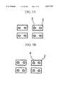
- FIG. 3is a schematic view illustrative of the individual chip.
- the size of the individual recessed portion 32has to be larger than the semiconductor element 27 by about 200 micrometers to form a space for the wirings 28 and in consideration of an accuracy of alignment of the cap. For this reason, it is difficult to reduce the size of the recessed portion near the semiconductor element size.
- the rate of mounting of the elements 27 onto the mother board 24is as fast as 0.6 seconds per unit. It is difficult to obtain a remarkable increase in the rate of the mounting of the elements 27.
- the productivity of the semiconductor chips 41is limited by the rate of the mounting of the elements 27. For this reason, it is difficult to obtain a remarkable increase in the productivity of the semiconductor elements.
- a method of fabricating a chip semiconductor devicecomprises the following steps.
- electrically conductive bumpsare provided on electrodes of semiconductor elements on a wafer.
- an insulating substrate having an electrode patternis combined onto the wafer so that the electrode pattern is made into contact with the bumps.
- only the wafer on which the semiconductor elements are providedis divided by grooves into a plurality of chips each of which has a semiconductor element.
- a liquid resinis flowed into the grooves and onto the chips for subsequent curing the resin.
- the cured resin and the insulating substrateare concurrently cut along the grooves so that a plurality of semiconductor devices are formed.
- the shape and the size of the insulating substrateare the same as the semiconductor wafer because the electrode pattern of the insulating substrate is bonded to the bumps of the semiconductor elements.
- a method of fabricating a chip semiconductor devicecomprises the following steps.
- a first resinis applied on a first surface of a semiconductor wafer having a second surface on which a plurality of semiconductor elements have already been provided, which have a predetermined electrode pattern, before the applied resin is cured.
- an insulating substrateis combined onto the first surface of the semiconductor wafer.
- via holes and dicing recognition patternsare formed in the insulating substrate so that the electrode pattern is partially shown through the via holes.
- electrically conductive bumpsare formed, which are connected through the via holes to the electrode pattern.
- the dicing recognition patternis used to form grooves in the combined semiconductor wafer and the insulating substrate so as to divide the combined semiconductor wafer and the insulating substrate into a plurality of parts by the grooves.
- a second resinis filled into the grooves and then cured.
- the combined semiconductor wafer and the insulating substrateare cut off along the grooves filled with the second resin so that the combined semiconductor wafer and the insulating substrate are divided into a plurality of semiconductor devices.
- the dicing recognition patternis formed on the insulating substrate so that the combined semiconductor wafer and insulating substrate are divided by the groves which have been formed by use of the dicing recognition pattern, wherein the insulation substrate has no electrode pattern.
- the divided semiconductor deviceshave cross sections which are covered by and protected by the second resin.
- first and second resins prior to the curing processmay be the same resin material in a liquid state.
- the electrically conductive bumpsmay be made of a metal.
- FIG. 1is a cross sectional elevation view illustrative of a mother board to be used in a first step involved in the conventional fabrication processes for the chip semiconductor devices.
- FIG. 2is a cross sectional elevation view illustrative of a mother board and a sealing cap covering the mother board in a second step involved in the conventional fabrication processes for the chip semiconductor devices.
- FIG. 3is a schematic view illustrative of a chip semiconductor device fabricated by the conventional processes of FIGS. 1 and 2.
- FIGS. 4A through 4Fare schematic views illustrative of sequential steps involved in a novel method of forming a plurality of semiconductor devices from a semiconductor wafer in accordance with the present invention.
- FIGS. 5A through 5Care supplemental views illustrative of sequential steps involved in a novel method of forming a plurality of semiconductor devices from a semiconductor wafer in accordance with the present invention.
- FIG. 6is a schematic view illustrative of a chip semiconductor device fabricated by the novel processes of FIGS. 4A through 4F and 5A through 5C.
- FIGS. 7A through 7Fare fragmentary cross sectional elevation views illustrative of another novel method of forming a plurality of semiconductor devices from a semiconductor wafer in accordance with the present invention.
- FIG. 8is a fragmentary cross sectional elevation view illustrative of still another novel method of forming a plurality of semiconductor devices from a semiconductor wafer in accordance with the present invention.
- FIG. 4Aa semiconductor wafer 1 is prepared which has a plurality of semiconductor devices 2.
- the semiconductor wafer 1has an orientation flat 8.
- Each of the semiconductor devices 2has electrodes 3 as illustrated in FIG. 5A.
- metal bumpsare formed on the semiconductor devices 2.
- the metal bumps 4may be formed by ball bump method or solder bump printing method, any other method of forming the metal bumps may be used.
- FIG. 4Can insulation substrate 5 with an orientation flat 8' is prepared, which has electrode patterns before the insulation substrate 5 is then combined onto the semiconductor wafer 1 so that the electrode patterns contact the metal bumps 4.
- FIG. 5Cis illustrative of electrode patterns 6 formed on the insulation substrate 5. Grooves 7 have been formed in the insulating substrate 5 before metallization for forming the electrode patterns 6 extending through the grooves 7 to the opposite surface. Alternatively, the electrode patterns 6 may be formed which extend through the through holes.
- the electrode patterns 6are formed by positioning of the electrode patterns 6 over the insulating substrate 5 on the basis of positional coordinate data of the electrodes 3 of the semiconductor devices 2 over the semiconductor wafer 1.
- the insulating substrate 5has the same size and shape as the semiconductor wafer 1.
- the insulating substrate 5also has the same size orientation flat 8' as the orientation flat 8 of the semiconductor wafer 1.
- the electrode patterns 6are formed by printing method at the corresponding positions to the electrodes 3 of the semiconductor wafer 1.
- the alignment between the bumps and the electrode patternsmay be made by an alignment of the orientation flats 8 and 8'.
- the insulating substrate 5 and the semiconductor wafer 1are bonded by an insulating adhesive material.
- dicing grooves 9are formed only in the semiconductor wafer 1 so that only the semiconductor wafer 1 is cut to divide the same into the same size as the semiconductor devices 2' by use of the positional coordinate data of the semiconductor devices 2.
- a dicing sawmay be used to cut the semiconductor wafer 1.
- the diving groves 9may have a width of about 60 micrometers.
- a sealing resin 10 in liquid stateis flowed into the dicing grooves 9 and onto the semiconductor devices 2' before the curing the sealing resin 10 by a thermosetting process or a photo-curing process.
- the combined semiconductor wafer 1 and the insulating substrate 5are cut by further dicing process along the dicing grooves 9' to form dicing grooves 9' which divide the same into a plurality of chip semiconductor devices.
- the width of the dicing grooves 9'may be about 20 micrometers.
- chip semiconductor devices 12are formed as illustrated in FIG. 6.
- the semiconductor device 2is coated by the resin and is placed on the divided insulating substrate 5'. Cut sections 11 of the chip semiconductor devices are defined by the dicing grooves 9'.
- the semiconductor wafer 1 having been formed thereon with a plurality of the semiconductor devices 2is combined onto the insulating substrate 5 having been formed with the electrode patterns 6 so as to realize a highly accurate alignment between the bumps and the electrode patterns. Further the uniformly thin resin layer 10 has been formed to seal the semiconductor devices 2 before the cutting or dicing the semiconductor wafer combined with the insulating substrate, for which reason it is possible that the size of the chip semiconductor devices 12 may be reduced to that of the semiconductor devices 2.
- the productivity per a unitis remarkably increased. If, for example, about 70,000 elements are provided on the semiconductor wafer of 125 millimeters in diameter and it takes 5 minutes to bond the semiconductor wafer onto the insulating substrate, then it takes 0.004 seconds per a unit to mount the semiconductor device onto the semiconductor wafer 1. This means that the productivity is improved by 150 times as compared to when the semiconductor devices are separately mounted onto the semiconductor wafer.
- the insulating substrate 5has to have the same size and shape as the semiconductor wafer 1 and also the electrode patterns are printed so that the electrode patterns are superimposed on the metal bumps 4 of the semiconductor devices 2.
- the positional coordinate data of the electrodes 3 of the semiconductor devices 2 over the semiconductor wafer 1are read out by passing a light through the insulating substrate 5, for which reason a difference in reflective index may cause variations in the positional data on coordinate.
- the semiconductor wafer 1is bonded with the insulating substrate 5 and a distance between the semiconductor wafer 1 and the insulating substrate 5 is small, for which reason the semiconductor wafer 1 is broken in the dicing process.
- FIGS. 7A through 7FA second embodiment according to the present invention will be described in detail with reference to FIGS. 7A through 7F wherein a novel method of fabricating chip semiconductor devices will be described which is free from the above disadvantages as described in the first embodiment.
- a semiconductor wafer 14has on its first surface a plurality of semiconductor devices 15.
- a resin in a liquid stateis applied onto a second surface of the semiconductor wafer 14 for subsequent curing of the resin to form a uniformly thin resin layer 17 on the second surface of the semiconductor wafer 14.
- Electrode patterns 16are formed on the semiconductor devices 2 over the semiconductor wafer 14.
- An insulating substrate 18 free of electrode patternis bonded onto the electrode patterns 16 on the semiconductor devices 2 over the semiconductor wafer 14.
- a photo-resist pattern 13is provided on the insulating substrate 18.
- the semiconductor wafer 14may comprise a GaAs wafer of 100 micrometers in thickness.
- the insulating substrate 18may comprise a highly resistive GaAs substrate of 100 micrometer sin thickness. Polyimide and photo-resist may be available for bonding the insulating substrate to the semiconductor wafer.
- the photo-resist pattern 13is used as a mask for subsequent etching of the insulating substrate 18 to form via holes 19 and dicing recognition patterns 20 in the insulating substrate 18 before the used photo-resist mask is removed.
- the electrode patterns 16are partially shown.
- the electrode patternscomprise 80 micrometers squares.
- the via holemay be shaped in 40 micrometers square.
- the via holesmay be formed by dry etching process using the photo-resist technique.
- the alignment of the via hole patterns and the electrode patternsis made by use of the infrared ray. If any displacement between them can be detected, then the above process is made again until the accurate alignment can be obtained.
- metal bumps 21are formed on the electrode patterns 16 through the via holes 19 for allowance of the connection to external element.
- the semiconductor wafer 14 and the insulating substrate 18are cut or diced to ensure the size of the semiconductor device 15 whereby the cured resin 17 is shown through dicing regions 22.
- the dicing recognition patterns 20can directly be recognized whereby the dicing positions can accurately be decided. No problem is raised with misrecognition in the operation of the automatic recognizing dicing system.
- the dicing widthmay be 150 micrometers.
- the dicing recognition pattern 20may be formed in the insulating substrate 18. In this case, the dicing recognition pattern 20 remains after the dicing process.
- a resin 17'is flowed into the diced region 22 and also onto the cured resin layer 17 as well as onto the sides of the semiconductor devices 15 and the insulation substrate 18 before the resin 17' is cured.
- the resin 17'securely contacts with cured resin layer 17.
- the resin 17' having floweddoes not reach the sides of the electrode patterns 16 because of a small gap between the semiconductor wafer 14 and the insulating substrate 18.
- the dicing widthmay be 30 micrometers.
- the cured resins 17 and 17'are concurrently cut to divide the semiconductor devices into individuals whereby the chip semiconductor devices having near size as the semiconductor devices are formed.
- the dicing width of FIG. 7Fis narrower than the dicing width of FIG. 7D so that the resin 17' remains on the sides of the diced semiconductor devices 15 and the insulating substrate 18.
- the alignment of the electrode pattern 16 to form the via holes 19is made by use of the alignment recognition pattern wherein an infrared ray transmission microscope is used to read out the recognition pattern. In this case, it might be possible that opening positions of the photo-resist 13 for forming the via holes 19 are displaced in a direction of arrow mark "X" from the position of the electrode pattern 16 due to refractive index of the insulation substrate 18 and others.
- lead electrodes 23may be connected to the metal bumps 21.
- the shape and the size of the insulating substrateare the same as the semiconductor wafer because the electrode pattern of the insulating substrate is bonded to the bumps of the semiconductor elements.
Landscapes
- Engineering & Computer Science (AREA)
- Computer Hardware Design (AREA)
- Microelectronics & Electronic Packaging (AREA)
- Power Engineering (AREA)
- Physics & Mathematics (AREA)
- Condensed Matter Physics & Semiconductors (AREA)
- General Physics & Mathematics (AREA)
- Manufacturing & Machinery (AREA)
- Dicing (AREA)
- Encapsulation Of And Coatings For Semiconductor Or Solid State Devices (AREA)
Abstract
Description
Claims (12)
Applications Claiming Priority (2)
| Application Number | Priority Date | Filing Date | Title |
|---|---|---|---|
| JP9-125408 | 1997-05-15 | ||
| JP9125408AJP2812326B2 (en) | 1996-08-09 | 1997-05-15 | Manufacturing method of chip type semiconductor device |
Publications (1)
| Publication Number | Publication Date |
|---|---|
| US6077757Atrue US6077757A (en) | 2000-06-20 |
Family
ID=14909382
Family Applications (1)
| Application Number | Title | Priority Date | Filing Date |
|---|---|---|---|
| US09/020,789Expired - Fee RelatedUS6077757A (en) | 1997-05-15 | 1998-02-09 | Method of forming chip semiconductor devices |
Country Status (2)
| Country | Link |
|---|---|
| US (1) | US6077757A (en) |
| CN (1) | CN1106036C (en) |
Cited By (16)
| Publication number | Priority date | Publication date | Assignee | Title |
|---|---|---|---|---|
| US6303471B1 (en)* | 1998-10-14 | 2001-10-16 | Nippon Telegraph And Telephone Corporation | Method of manufacturing semiconductor device having reinforcing member and method of manufacturing IC card using the device |
| US20010052642A1 (en)* | 2000-06-16 | 2001-12-20 | Wood Alan G. | Semiconductor device package and method |
| WO2002058131A1 (en)* | 2001-01-22 | 2002-07-25 | Stmicroelectronics Sa | Method for making a semiconductor package and semiconductor package with integrated circuit chips |
| US6538317B1 (en)* | 1999-07-30 | 2003-03-25 | Sharp Kabushiki Kaisha | Substrate for resin-encapsulated semiconductor device, resin-encapsulated semiconductor device and process for fabricating the same |
| US6590291B2 (en)* | 2000-01-31 | 2003-07-08 | Shinko Electric Industries Co., Ltd. | Semiconductor device and manufacturing method therefor |
| WO2003060999A1 (en)* | 2002-01-17 | 2003-07-24 | Infineon Technologies Ag | Electronic component and panel and method for the production thereof |
| US20030201531A1 (en)* | 2000-06-08 | 2003-10-30 | Farnworth Warren M. | Semiconductor devices including protective layers on active surfaces thereof |
| US6815313B2 (en)* | 1999-06-02 | 2004-11-09 | Japan Radio Co., Ltd. | Electronic component to be mounted on a circuit board having electronic circuit device sealed therein and method of manufacturing the same |
| US6900532B1 (en)* | 2000-09-01 | 2005-05-31 | National Semiconductor Corporation | Wafer level chip scale package |
| US20060006760A1 (en)* | 2001-02-06 | 2006-01-12 | Akihiko Namba | Surface acoustic wave device, its manufacturing method, and electronic circuit device |
| US20060154447A1 (en)* | 2005-01-13 | 2006-07-13 | Yoshimasa Kushima | Method for manufacturing semiconductor device |
| KR100738149B1 (en) | 2005-03-29 | 2007-07-10 | 산요덴키가부시키가이샤 | Semiconductor device and manufacturing method thereof |
| US20070262462A1 (en)* | 2006-05-11 | 2007-11-15 | Matsushita Electric Industrial Co., Ltd. | Manufacturing method of resin-molding type semiconductor device, and wiring board therefor |
| US20090075457A1 (en)* | 2007-09-18 | 2009-03-19 | Shinko Electric Industries Co., Ltd. | Manufacturing method of semiconductor apparatus |
| US7510908B1 (en) | 2003-02-20 | 2009-03-31 | National Semiconductor Corporation | Method to dispense light blocking material for wafer level CSP |
| US8242616B1 (en)* | 2008-08-29 | 2012-08-14 | Renesas Electronics Corporation | Method for manufacturing semiconductor device and molded structure |
Families Citing this family (5)
| Publication number | Priority date | Publication date | Assignee | Title |
|---|---|---|---|---|
| CN1332430C (en)* | 2000-11-17 | 2007-08-15 | 矽品精密工业股份有限公司 | Integrated Circuit Packaging Unit Segmentation Method |
| JP4137471B2 (en)* | 2002-03-04 | 2008-08-20 | 東京エレクトロン株式会社 | Dicing method, integrated circuit chip inspection method, and substrate holding apparatus |
| JP2004273895A (en)* | 2003-03-11 | 2004-09-30 | Disco Abrasive Syst Ltd | Method of dividing semiconductor wafer |
| JP4063277B2 (en)* | 2004-12-21 | 2008-03-19 | セイコーエプソン株式会社 | Manufacturing method of semiconductor device |
| CN104362100B (en)* | 2014-10-15 | 2017-11-14 | 申宇慈 | Method for manufacturing functional substrate and functional substrate |
Citations (15)
| Publication number | Priority date | Publication date | Assignee | Title |
|---|---|---|---|---|
| US4468857A (en)* | 1983-06-27 | 1984-09-04 | Teletype Corporation | Method of manufacturing an integrated circuit device |
| US4864514A (en)* | 1986-09-02 | 1989-09-05 | Kabushiki Kaisha Toshiba | Wire-bonding method and apparatus |
| US4904610A (en)* | 1988-01-27 | 1990-02-27 | General Instrument Corporation | Wafer level process for fabricating passivated semiconductor devices |
| US5020715A (en)* | 1987-12-23 | 1991-06-04 | Kabushiki Kaisha Shinkawa | Bonding method |
| US5266528A (en)* | 1991-09-17 | 1993-11-30 | Fujitsu Limited | Method of dicing semiconductor wafer with diamond and resin blades |
| US5323051A (en)* | 1991-12-16 | 1994-06-21 | Motorola, Inc. | Semiconductor wafer level package |
| US5373627A (en)* | 1993-11-23 | 1994-12-20 | Grebe; Kurt R. | Method of forming multi-chip module with high density interconnections |
| US5547906A (en)* | 1992-09-14 | 1996-08-20 | Badehi; Pierre | Methods for producing integrated circuit devices |
| US5561085A (en)* | 1994-12-19 | 1996-10-01 | Martin Marietta Corporation | Structure for protecting air bridges on semiconductor chips from damage |
| US5604160A (en)* | 1996-07-29 | 1997-02-18 | Motorola, Inc. | Method for packaging semiconductor devices |
| US5757068A (en)* | 1994-09-30 | 1998-05-26 | Nec Corporation | Carrier film with peripheral slits |
| US5851845A (en)* | 1995-12-18 | 1998-12-22 | Micron Technology, Inc. | Process for packaging a semiconductor die using dicing and testing |
| US5863813A (en)* | 1997-08-20 | 1999-01-26 | Micron Communications, Inc. | Method of processing semiconductive material wafers and method of forming flip chips and semiconductor chips |
| US5866950A (en)* | 1993-09-01 | 1999-02-02 | Kabushiki Kaisha Toshiba | Semiconductor package and fabrication method |
| US5949140A (en)* | 1996-05-30 | 1999-09-07 | Oki Electric Industry Co., Ltd. | Microwave semiconductor device with via holes and associated structure |
Family Cites Families (3)
| Publication number | Priority date | Publication date | Assignee | Title |
|---|---|---|---|---|
| JP2967215B2 (en)* | 1990-10-12 | 1999-10-25 | 株式会社村田製作所 | Manufacturing method of chip-type electronic components |
| JP3128878B2 (en)* | 1991-08-23 | 2001-01-29 | ソニー株式会社 | Semiconductor device |
| JPH088278A (en)* | 1994-06-20 | 1996-01-12 | Hitachi Ltd | Method for manufacturing semiconductor device |
- 1998
- 1998-02-09USUS09/020,789patent/US6077757A/ennot_activeExpired - Fee Related
- 1998-02-09CNCN98100405Apatent/CN1106036C/ennot_activeExpired - Fee Related
Patent Citations (15)
| Publication number | Priority date | Publication date | Assignee | Title |
|---|---|---|---|---|
| US4468857A (en)* | 1983-06-27 | 1984-09-04 | Teletype Corporation | Method of manufacturing an integrated circuit device |
| US4864514A (en)* | 1986-09-02 | 1989-09-05 | Kabushiki Kaisha Toshiba | Wire-bonding method and apparatus |
| US5020715A (en)* | 1987-12-23 | 1991-06-04 | Kabushiki Kaisha Shinkawa | Bonding method |
| US4904610A (en)* | 1988-01-27 | 1990-02-27 | General Instrument Corporation | Wafer level process for fabricating passivated semiconductor devices |
| US5266528A (en)* | 1991-09-17 | 1993-11-30 | Fujitsu Limited | Method of dicing semiconductor wafer with diamond and resin blades |
| US5323051A (en)* | 1991-12-16 | 1994-06-21 | Motorola, Inc. | Semiconductor wafer level package |
| US5547906A (en)* | 1992-09-14 | 1996-08-20 | Badehi; Pierre | Methods for producing integrated circuit devices |
| US5866950A (en)* | 1993-09-01 | 1999-02-02 | Kabushiki Kaisha Toshiba | Semiconductor package and fabrication method |
| US5373627A (en)* | 1993-11-23 | 1994-12-20 | Grebe; Kurt R. | Method of forming multi-chip module with high density interconnections |
| US5757068A (en)* | 1994-09-30 | 1998-05-26 | Nec Corporation | Carrier film with peripheral slits |
| US5561085A (en)* | 1994-12-19 | 1996-10-01 | Martin Marietta Corporation | Structure for protecting air bridges on semiconductor chips from damage |
| US5851845A (en)* | 1995-12-18 | 1998-12-22 | Micron Technology, Inc. | Process for packaging a semiconductor die using dicing and testing |
| US5949140A (en)* | 1996-05-30 | 1999-09-07 | Oki Electric Industry Co., Ltd. | Microwave semiconductor device with via holes and associated structure |
| US5604160A (en)* | 1996-07-29 | 1997-02-18 | Motorola, Inc. | Method for packaging semiconductor devices |
| US5863813A (en)* | 1997-08-20 | 1999-01-26 | Micron Communications, Inc. | Method of processing semiconductive material wafers and method of forming flip chips and semiconductor chips |
Cited By (31)
| Publication number | Priority date | Publication date | Assignee | Title |
|---|---|---|---|---|
| US6303471B1 (en)* | 1998-10-14 | 2001-10-16 | Nippon Telegraph And Telephone Corporation | Method of manufacturing semiconductor device having reinforcing member and method of manufacturing IC card using the device |
| US6815313B2 (en)* | 1999-06-02 | 2004-11-09 | Japan Radio Co., Ltd. | Electronic component to be mounted on a circuit board having electronic circuit device sealed therein and method of manufacturing the same |
| US6538317B1 (en)* | 1999-07-30 | 2003-03-25 | Sharp Kabushiki Kaisha | Substrate for resin-encapsulated semiconductor device, resin-encapsulated semiconductor device and process for fabricating the same |
| US6964887B2 (en) | 2000-01-31 | 2005-11-15 | Shinko Electronic Industries Co., Ltd. | Method for manufacturing semiconductor device |
| US20030209806A1 (en)* | 2000-01-31 | 2003-11-13 | Shinko Electric Industries Co., Ltd. | Method for manufacturing semiconductor device |
| US6590291B2 (en)* | 2000-01-31 | 2003-07-08 | Shinko Electric Industries Co., Ltd. | Semiconductor device and manufacturing method therefor |
| US20030201531A1 (en)* | 2000-06-08 | 2003-10-30 | Farnworth Warren M. | Semiconductor devices including protective layers on active surfaces thereof |
| US20050101158A1 (en)* | 2000-06-08 | 2005-05-12 | Farnworth Warren M. | Methods for forming protective layers on semiconductor device substrates |
| US20060197235A1 (en)* | 2000-06-08 | 2006-09-07 | Farnworth Warren M | Electronic device components including protective layers on surfaces thereof |
| US7084013B2 (en) | 2000-06-08 | 2006-08-01 | Micron Technology, Inc. | Methods for forming protective layers on semiconductor device substrates |
| US7067901B2 (en)* | 2000-06-08 | 2006-06-27 | Micron Technology, Inc. | Semiconductor devices including protective layers on active surfaces thereof |
| US6911737B2 (en) | 2000-06-16 | 2005-06-28 | Micron Technology, Inc. | Semiconductor device package and method |
| US20010052642A1 (en)* | 2000-06-16 | 2001-12-20 | Wood Alan G. | Semiconductor device package and method |
| US7214566B1 (en)* | 2000-06-16 | 2007-05-08 | Micron Technology, Inc. | Semiconductor device package and method |
| US7241643B1 (en) | 2000-09-01 | 2007-07-10 | National Semiconductor Corporation | Wafer level chip scale package |
| US6900532B1 (en)* | 2000-09-01 | 2005-05-31 | National Semiconductor Corporation | Wafer level chip scale package |
| WO2002058131A1 (en)* | 2001-01-22 | 2002-07-25 | Stmicroelectronics Sa | Method for making a semiconductor package and semiconductor package with integrated circuit chips |
| FR2819936A1 (en)* | 2001-01-22 | 2002-07-26 | St Microelectronics Sa | METHOD FOR MANUFACTURING A SEMICONDUCTOR PACKAGE AND SEMICONDUCTOR PACKAGE WITH INTEGRATED CIRCUIT CHIPS |
| US20060006760A1 (en)* | 2001-02-06 | 2006-01-12 | Akihiko Namba | Surface acoustic wave device, its manufacturing method, and electronic circuit device |
| US7034383B2 (en) | 2002-01-17 | 2006-04-25 | Infineon Technologies Ag | Electronic component and panel and method for producing the same |
| US20050087889A1 (en)* | 2002-01-17 | 2005-04-28 | Stephan Blaszczak | Electronic component and panel and method for the production thereof |
| WO2003060999A1 (en)* | 2002-01-17 | 2003-07-24 | Infineon Technologies Ag | Electronic component and panel and method for the production thereof |
| US7510908B1 (en) | 2003-02-20 | 2009-03-31 | National Semiconductor Corporation | Method to dispense light blocking material for wafer level CSP |
| US20060154447A1 (en)* | 2005-01-13 | 2006-07-13 | Yoshimasa Kushima | Method for manufacturing semiconductor device |
| US7763528B2 (en)* | 2005-01-13 | 2010-07-27 | Oki Semiconductor Co., Ltd. | Method for manufacturing semiconductor device |
| KR100738149B1 (en) | 2005-03-29 | 2007-07-10 | 산요덴키가부시키가이샤 | Semiconductor device and manufacturing method thereof |
| US20070262462A1 (en)* | 2006-05-11 | 2007-11-15 | Matsushita Electric Industrial Co., Ltd. | Manufacturing method of resin-molding type semiconductor device, and wiring board therefor |
| US7504735B2 (en)* | 2006-05-11 | 2009-03-17 | Panasonic Corporation | Manufacturing method of resin-molding type semiconductor device, and wiring board therefor |
| US20090075457A1 (en)* | 2007-09-18 | 2009-03-19 | Shinko Electric Industries Co., Ltd. | Manufacturing method of semiconductor apparatus |
| US7772091B2 (en)* | 2007-09-18 | 2010-08-10 | Shinko Electric Industries Co., Ltd. | Manufacturing method of semiconductor apparatus comprising alignment patterns in scribe regions |
| US8242616B1 (en)* | 2008-08-29 | 2012-08-14 | Renesas Electronics Corporation | Method for manufacturing semiconductor device and molded structure |
Also Published As
| Publication number | Publication date |
|---|---|
| CN1106036C (en) | 2003-04-16 |
| CN1199924A (en) | 1998-11-25 |
Similar Documents
| Publication | Publication Date | Title |
|---|---|---|
| US6077757A (en) | Method of forming chip semiconductor devices | |
| US7456083B2 (en) | Semiconductor device and manufacturing method of the same | |
| US6759745B2 (en) | Semiconductor device and manufacturing method thereof | |
| US6207473B1 (en) | Process for manufacturing semiconductor wafer, process for manufacturing semiconductor chip, and IC card | |
| US7045908B2 (en) | Semiconductor device and method for manufacturing the same | |
| US9048352B2 (en) | Solid image-pickup device with flexible circuit substrate | |
| EP2050130B1 (en) | Transponder and method of producing a transponder | |
| KR20090029660A (en) | Manufacturing Method of Semiconductor Device | |
| US7884453B2 (en) | Semiconductor device and manufacturing method thereof | |
| CN114256170B (en) | Fan-out packaging structure and preparation method thereof | |
| EP2897163B1 (en) | Semiconductor device and method of manufacturing a semiconductor device | |
| US7053492B2 (en) | Circuit device and method of manufacturing the same | |
| US8072068B2 (en) | Semiconductor device and a method for manufacturing the same | |
| US20070007666A1 (en) | Substrate for manufacturing semiconductor device, semiconductor device manufacturing method | |
| US11296034B2 (en) | Substrate and semiconductor package comprising an interposer element with a slot and method of manufacturing the same | |
| CN111048468B (en) | Laminate of electronic component and method for manufacturing the same | |
| US5485337A (en) | Thin film magnetic head structure and method of fabricating the same for accurately locating and connecting terminals to terminal connections | |
| US20090162975A1 (en) | Method of forming a wafer level package | |
| JP2812326B2 (en) | Manufacturing method of chip type semiconductor device | |
| WO1990001215A1 (en) | Semiconductor device | |
| US20080224331A1 (en) | Electronic device and method for manufacturing the same | |
| US20090212400A1 (en) | Semiconductor device and manufacturing method and mounting method thereof | |
| JP2597809B2 (en) | Method for manufacturing semiconductor device | |
| KR100415687B1 (en) | Semiconductor Chip Scale Package and method of manufacturing the same | |
| WO1997007538A1 (en) | Method of making electrical connections to integrated circuit |
Legal Events
| Date | Code | Title | Description |
|---|---|---|---|
| AS | Assignment | Owner name:NEC CORPORATION, JAPAN Free format text:ASSIGNMENT OF ASSIGNORS INTEREST;ASSIGNORS:MIZUNO, HIDEKI;TOKUNAGA, KAZUNAO;REEL/FRAME:009007/0635 Effective date:19980206 | |
| FEPP | Fee payment procedure | Free format text:PAYOR NUMBER ASSIGNED (ORIGINAL EVENT CODE: ASPN); ENTITY STATUS OF PATENT OWNER: LARGE ENTITY | |
| AS | Assignment | Owner name:NEC COMPOUND SEMICONDUCTOR DEVICES, LTD., JAPAN Free format text:ASSIGNMENT OF ASSIGNORS INTEREST;ASSIGNOR:NEC CORPORATION;REEL/FRAME:013852/0613 Effective date:20020919 | |
| FPAY | Fee payment | Year of fee payment:4 | |
| AS | Assignment | Owner name:NEC ELECTRONICS CORPORATION, JAPAN Free format text:ASSIGNMENT OF ASSIGNORS INTEREST;ASSIGNOR:NEC COMPOUND SEMICONDUCTOR DEVICES, LTD.;REEL/FRAME:017422/0528 Effective date:20060315 | |
| REMI | Maintenance fee reminder mailed | ||
| LAPS | Lapse for failure to pay maintenance fees | ||
| STCH | Information on status: patent discontinuation | Free format text:PATENT EXPIRED DUE TO NONPAYMENT OF MAINTENANCE FEES UNDER 37 CFR 1.362 | |
| FP | Lapsed due to failure to pay maintenance fee | Effective date:20080620 |