US6077732A - Method of forming a thin film transistor - Google Patents
Method of forming a thin film transistorDownload PDFInfo
- Publication number
- US6077732A US6077732AUS09/074,634US7463498AUS6077732AUS 6077732 AUS6077732 AUS 6077732AUS 7463498 AUS7463498 AUS 7463498AUS 6077732 AUS6077732 AUS 6077732A
- Authority
- US
- United States
- Prior art keywords
- thin film
- area
- drain
- channel
- layer
- Prior art date
- Legal status (The legal status is an assumption and is not a legal conclusion. Google has not performed a legal analysis and makes no representation as to the accuracy of the status listed.)
- Expired - Lifetime
Links
Images


Classifications
- H—ELECTRICITY
- H10—SEMICONDUCTOR DEVICES; ELECTRIC SOLID-STATE DEVICES NOT OTHERWISE PROVIDED FOR
- H10D—INORGANIC ELECTRIC SEMICONDUCTOR DEVICES
- H10D30/00—Field-effect transistors [FET]
- H10D30/01—Manufacture or treatment
- H10D30/021—Manufacture or treatment of FETs having insulated gates [IGFET]
- H10D30/031—Manufacture or treatment of FETs having insulated gates [IGFET] of thin-film transistors [TFT]
- H10D30/0312—Manufacture or treatment of FETs having insulated gates [IGFET] of thin-film transistors [TFT] characterised by the gate electrodes
- H10D30/0316—Manufacture or treatment of FETs having insulated gates [IGFET] of thin-film transistors [TFT] characterised by the gate electrodes of lateral bottom-gate TFTs comprising only a single gate
- H—ELECTRICITY
- H10—SEMICONDUCTOR DEVICES; ELECTRIC SOLID-STATE DEVICES NOT OTHERWISE PROVIDED FOR
- H10D—INORGANIC ELECTRIC SEMICONDUCTOR DEVICES
- H10D30/00—Field-effect transistors [FET]
- H10D30/01—Manufacture or treatment
- H10D30/021—Manufacture or treatment of FETs having insulated gates [IGFET]
- H10D30/031—Manufacture or treatment of FETs having insulated gates [IGFET] of thin-film transistors [TFT]
- H10D30/0321—Manufacture or treatment of FETs having insulated gates [IGFET] of thin-film transistors [TFT] comprising silicon, e.g. amorphous silicon or polysilicon
- H—ELECTRICITY
- H10—SEMICONDUCTOR DEVICES; ELECTRIC SOLID-STATE DEVICES NOT OTHERWISE PROVIDED FOR
- H10D—INORGANIC ELECTRIC SEMICONDUCTOR DEVICES
- H10D30/00—Field-effect transistors [FET]
- H10D30/60—Insulated-gate field-effect transistors [IGFET]
- H10D30/67—Thin-film transistors [TFT]
- H10D30/6704—Thin-film transistors [TFT] having supplementary regions or layers in the thin films or in the insulated bulk substrates for controlling properties of the device
- H10D30/6713—Thin-film transistors [TFT] having supplementary regions or layers in the thin films or in the insulated bulk substrates for controlling properties of the device characterised by the properties of the source or drain regions, e.g. compositions or sectional shapes
- H10D30/6715—Thin-film transistors [TFT] having supplementary regions or layers in the thin films or in the insulated bulk substrates for controlling properties of the device characterised by the properties of the source or drain regions, e.g. compositions or sectional shapes characterised by the doping profiles, e.g. having lightly-doped source or drain extensions
- H10D30/6717—Thin-film transistors [TFT] having supplementary regions or layers in the thin films or in the insulated bulk substrates for controlling properties of the device characterised by the properties of the source or drain regions, e.g. compositions or sectional shapes characterised by the doping profiles, e.g. having lightly-doped source or drain extensions the source and the drain regions being asymmetrical
- H—ELECTRICITY
- H10—SEMICONDUCTOR DEVICES; ELECTRIC SOLID-STATE DEVICES NOT OTHERWISE PROVIDED FOR
- H10D—INORGANIC ELECTRIC SEMICONDUCTOR DEVICES
- H10D30/00—Field-effect transistors [FET]
- H10D30/60—Insulated-gate field-effect transistors [IGFET]
- H10D30/67—Thin-film transistors [TFT]
- H10D30/6729—Thin-film transistors [TFT] characterised by the electrodes
- H10D30/673—Thin-film transistors [TFT] characterised by the electrodes characterised by the shapes, relative sizes or dispositions of the gate electrodes
- H10D30/6733—Multi-gate TFTs
- H10D30/6734—Multi-gate TFTs having gate electrodes arranged on both top and bottom sides of the channel, e.g. dual-gate TFTs
- Y—GENERAL TAGGING OF NEW TECHNOLOGICAL DEVELOPMENTS; GENERAL TAGGING OF CROSS-SECTIONAL TECHNOLOGIES SPANNING OVER SEVERAL SECTIONS OF THE IPC; TECHNICAL SUBJECTS COVERED BY FORMER USPC CROSS-REFERENCE ART COLLECTIONS [XRACs] AND DIGESTS
- Y10—TECHNICAL SUBJECTS COVERED BY FORMER USPC
- Y10S—TECHNICAL SUBJECTS COVERED BY FORMER USPC CROSS-REFERENCE ART COLLECTIONS [XRACs] AND DIGESTS
- Y10S438/00—Semiconductor device manufacturing: process
- Y10S438/91—Controlling charging state at semiconductor-insulator interface
Definitions
- This inventionrelates to methods of forming thin film transistors.
- TFTthin film transistors
- a thin film of semiconductive materialis first provided.
- a central channel region of the thin filmis masked, while opposing adjacent source/drain regions are doped with an appropriate p or n type conductivity enhancing impurity.
- a gate insulator and gateare provided either above or below the thin film channel region, thus providing a field effect transistor having an active channel region formed entirely within a thin film as opposed to a bulk semiconductor substrate.
- a static memory cellis characterized by operation in one of two mutually exclusive and cell-maintaining operating states. Each operating state defines one of the two possible binary bit values, 0 or 1.
- a static memory celltypically has an output which reflects the operating state of the memory cell. Such an output produces a "high” voltage to indicate a "set” operating state. The memory cell output produces a "low” voltage to indicate a "reset” memory cell operating state.
- a low or reset output voltageusually represents a binary value of 0, and a high or set output voltage represents a binary value of 1.
- a static memory cellis said to be bi-stable because it has two stable or self-maintaining operating states, corresponding to two different output voltages. Without external stimuli, a static memory cell will operate continuously in a single one of its two operating states. It has internal feedback to maintain a stable output voltage, corresponding to operating states of the memory cell, as long as the memory cell receives power.
- a dynamic memory cellcan be programmed to store a voltage which represents one of two binary values, but requires periodic reprogramming or "refreshing" to maintain this voltage for more than very short time periods.
- a dynamic memory cellhas no feedback to maintain a stable output voltage. Without refreshing, the output of a dynamic memory cell will drift towards intermediate or indeterminate voltages, effectively resulting in loss of data.
- Dynamic memory cellsare used in spite of this limitation because of the significantly greater packaging densities which can be attained.
- a dynamic memory cellcan be fabricated with a single MOSFET transistor, rather than the six transistors typically required in a static memory cell.
- SRAM cell densitycan be maximized with three-dimensional integration.
- load transistors of the SRAM cellconstitute TFTs which are folded over the bulk transistors.
- polysiliconOne common material utilized as the thin source, channel and drain film in a TFT is polysilicon. Such is comprised of multiple forms of individual single crystal silicon grains. The locations where two individual crystalline grains abut one another is commonly referred to as a grain boundary. Grain boundaries are inherent in polycrystalline materials, such as polysilicon, as it is the boundaries which define the breaks between individual crystal grains. The crystalline structure breaks down at the grain boundaries, giving rise to a high concentration of broken or "dangling" Si bonds. These dangling bonds "trap" carriers and give rise to potential barriers at the grain boundaries. These potential a barriers impede the flow of carriers in polysilicon, thus reducing conductivity compared to bulk silicon.
- the grain boundary potential barrier heightis proportional to the square of the dangling bond density, or "trap density". The smaller the grain size, the higher the trap density and thus the lower the conductance.
- the grain boundary potential barrier height in the channelis controlled by the gate voltage, and hence the conductivity is a function of the gate voltage.
- the TFTshowever, have a lower drive compared to bulk transistors because of lower mobility in the channel and higher V t due to the larger trap concentration.
- the grain boundary trap concentrationalso affects the leakage current or the OFF current in TFTs.
- the presence of grain boundary traps at the drain endcan dramatically increase the leakage current and the presence of a "gate-to-drain” electric field.
- the increase in leakageresults from either "thermionic field emission” and/or "Poole-Frenkel" emission through the grain boundary traps.
- the greater the number of grain boundariesi.e., the smaller the grain size
- Greater current leakagemeans that more power is required to replace the leaking current to maintain an SRAM cell transistor in its desired powered-on state. Such leakage is particularly adverse in laptop computers, where desired power consumption when a cell's state is not being changed would be desired to be very low to extend battery life.
- High density SRAMs(16 Mb or higher) typically require TFTs with low OFF currents ( ⁇ 50 fA) and high ON current (>5 nA) in order to obtain acceptable low standby leakage and high memory cell stability.
- Current state-of-the-art TFTsprovide low standby current at the expense of ON current, or at the expense of additional process complexity.
- One present way of minimizing this current leakage at the cost of increased process complexityis by providing a "lightly doped offset" (LDO) region within the thin film.
- LDOlightly doped offset region is an elongated region within the thin film which is positioned effectively between the channel region and the drain region and is not under direct gate control but is affected by the sole fringing fields. Such a region provides a buffer zone for the electric field between the channel and drain which minimizes leakage therebetween.
- One prior art manner of contending with problems associated with grains boundariesis to "passivate" such boundaries after their formation.
- One techniqueinvolves exposing the thin film polycrystalline layer to atomic or plasma hydrogen, with the intent being to produce silicon-hydrogen bonds instead of dangling bonds at the boundary interfaces.
- An alternate techniqueis to implant F into the thin film polycrystalline layer in an effort to produce silicon-fluorine bonds at the boundary interfaces.
- a silicon-fluorine bondis much more desirable than a silicon hydrogen bond due to increased high temperature stability.
- the ion implantation technique of providing fluorine into a polycrystalline thin filmis not without drawbacks. For example, the implantation undesirably damages the thin film layer and typically creates more dangling bonds inherent from the implantation process. It also is not particularly effective in putting the F at the grain boundaries where it is required.
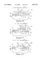
- FIG. 1illustrates a semiconductor wafer fragment 10 comprised of a substrate 12.
- An insulating layer 13is provided thereover, and includes an intervening or embedded electrically conductive transistor gate 14. That portion of substrate 12 immediately beneath layer 13 and gate 14 would comprise an insulator material.
- a gate dielectric layer 16overlies insulating layer 13 and gate 14. Further, a thin film transistor layer 18 is provided over gate dielectric layer 16.
- thin film transistor layer 18 iiis subjected to a blanket implant, in this described example an n-type material, to some suitable first low concentration, such as 5 ⁇ 10 17 ions/cm 3 -5 ⁇ 10 18 ions/cm 3 .
- the function of the blanket implantis to provide desired resultant semiconductivity for the channel region of the transistor.
- a mask 19is provided over thin film transistor layer 18 to define a desired n- channel region 20 overlying gate 14. Wafer 10 is then subjected to p-type doping to provide an example p- implant concentration outside of mask 19 to provide an example p- concentration of from 5 ⁇ 10 18 ions/cm 3 5 ⁇ 10 19 ions/cm 3 . The purpose of such implant is to overwhelm the concentration of the blanket n- implant previously provided to produce a desired drain offset region.
- channel region 20 and what becomes a desired drain offset region 24are masked with a photoresist masking block 25.
- Wafer fragment 10is then subjected to heavy p-type doping to provide a resultant p+ concentration of for example greater than or equal to 1 ⁇ 10 20 ions/cm 3 .
- the resultis provision of desired source and drain regions 26 and 27, respectively. The effect is to produce a lighter doped drain offset region of the same conductivity type of the source and drain regions.
- FIG. 4depicts a processing step immediately subsequent to the FIG. 1 processing step of the first described embodiment.
- a masking block 19ais patterned to overlap or extend laterally beyond the confines of gate 14 to provide a source offset region 17 and a drain offset region 24a.
- the waferis then subjected to heavy p+ doping to produce the illustrated source and drain regions 26a and 27a, respectively. Therefore in accordance with this described prior art embodiment, the resultant drain offset region 24a is provided to be of the same identical concentration and conductivity type as that of channel region 22.
- FIG. 5illustrates a wafer fragment 10b shown at a processing step immediately subsequent to that depicted by FIG. 1 of the first described embodiment.
- a photoresist masking layer 19bis patterned to provide a contact opening 21 effective for producing a desired drain offset region 24.
- the wafer fragmentis then subjected to light p-type doping, yet to a concentration sufficient to overwhelm the n- concentration previously provided in drain offset region 24 by the FIG. 1 blanket implant.
- masking block 25is provided and the wafer subjected to p+ doping to effectively produce the same resultant prior art construction of FIG. 3.
- This inventionconcerns improved methods of forming thin film transistors having drain offsets as well as to an improved thin film transistor construction.
- FIG. 1is a diagrammatic sectional view of one prior art wafer fragment and discussed in the "Background” section above.
- FIG. 2is a view of the prior art FIG. 1 wafer at a prior art processing step subsequent to that shown by FIG. 1.
- FIG. 3is a view of the prior art FIG. 1 wafer at a prior art processing step subsequent to that shown by FIG. 2.
- FIG. 4is a diagrammatic sectional view of another prior art wafer fragment ad is discussed in the "Background" section above.
- FIG. 5is a diagrammatic sectional view of yet another prior art wafer fragment and is discussed in the "Background” section above.
- FIG. 6is a view of the prior art FIG. 5 wafer at a prior art processing step subsequent to that shown by FIG. 5.
- FIG. 7is a diagrammatic sectional view of a wafer fragment at one processing step in accordance with the invention.
- FIG. 8is a view of the FIG. 7 wafer at a processing step subsequent to that shown by FIG. 7.
- FIG. 9is a view of the FIG. 7 wafer at a processing step subsequent to that shown by FIG. 8.
- FIG. 10is a view of the FIG. 7 wafer at a processing step subsequent to that shown by FIG. 9.
- FIGS. 11-12are views of the FIG. 7 wafer at a processing step subsequent to that shown by FIG. 10.
- a method of forming a bottom gated thin film transistorcomprises the following steps:
- the thin film transistor layercomprising a source area, a channel area, a drain area, and a drain offset area;
- a semiconductor wafer fragment in process in a method of forming a bottom gated thin film transistor in accordance with the inventionis indicated generally with reference numeral 30.
- Suchcomprises a bulk semiconductor substrate 32 having an overlying insulator layer 34, such as SiO 2 . Collectively, such define an outer substrate surface 35.
- a gate 36is provided relative to substrate 32/34, and projects outwardly relative to outer surface 35.
- a gate dielectric layer 38is provided outwardly relative to surface 35 and transistor gate 36.
- a thin film transistor layer 40 of semiconductive materialis provided over gate dielectric layer 38.
- suchcomprises or defines a source area 41, a channel area 42, a drain area 44, and a drain offset area 43.
- a buffering etch stop layer 46is provided outwardly of thin film transistor layer 40.
- Suchpreferably comprises SiO 2 , with an example thickness being 100 Angstroms.
- Layer 40 at this point in the processis preferably doped with, for example, BF 2 to provide a p- desired implant concentration for an offset region to be formed relative to offset area 43.
- An example p-type implant concentrationis 1 ⁇ 10 17 -10 18 ions/cm 3 .
- a masking layer 50is provided over etch stop layer 46, and thus over thin film transistor layer 40.
- Masking layer 50 and thin film transistor layer 40preferably comprise the same predominate material, such as polysilicon. Doping concentration and type however might be different or non-existent, with layers 40 and 50 still essentially comprising the same predominate material.
- Other materials for layer 50are also contemplated, such as by way of example only, Si 3 N 4 , WSi x and SiO 2 .
- masking layer 50is anisotropically etched to define a first masking sidewall spacer 52 laterally adjacent transistor gate 36 over drain offset area 43 and a second masking sidewall spacer 54 laterally adjacent transistor gate 36 over or within source is area 41. Channel area 42 and remaining portions of source area 41 and drain area 44 are left effectively outwardly exposed.
- a conductivity enhancing impurity of a first typeis ion implanted into thin film channel area 42 of thin film transistor layer 40, thus defining a thin film channel region 56.
- An example and preferred dopant in accordance with the above described exampleis n-type, such as phosphorus, deposited to a concentration 10 times greater than the p-type implant of FIG. 7, with an example being 1 ⁇ 10 18 -1 ⁇ 10 19 ions/cm 3 .
- a fluorine containing layer 58is provided over first sidewall spacer 52, second sidewall spacer 54, etch stop layer 46, and thereby effectively over polycrystalline thin film layer 40.
- An example thickness for layer 58is 500 Angstroms.
- Wafer fragment 30, having fluorine containing layer 58,is then annealed at a temperature and for a time period which in combination are effective to drive fluorine from fluorine containing layer 58 into polycrystalline thin film layer 40 and incorporate fluorine within grain boundaries in layer 40 to passivate such grain boundaries.
- Buffering etch stop layer 46constitutes a buffering layer, with SiO 2 deposited to the above preferred thicknesses being effectively transmissive of fluorine ions from layer 58 into regions of thin film transistor layer 40 not covered by first and second masking spacers 52 and 54.
- layer 58preferably contains fluorine as an excess of fluorine in the form of free or loosely associated fluorine atoms.
- An example and preferred material for layer 58is WSi x provided by chemical vapor deposition utilizing WF 6 and SiH 4 as precursors. The fluorine from the WF 6 precursor will desirably be appreciably incorporated in layer 58.
- An example process for providing layer 58 by CVD using WF 6 and SiH 4 in a manner which maximizes incorporated fluorineincludes WF 6 and 30 sccm, Ar at 500 sccm, SiH 4 at 300 sccm, a temperature of 400° C. and a pressure of 1 Torr.
- fluorine containing layer 58might predominantly comprise elemental W having incorporated fluorine, such as by utilizing a CVD process also using WF 6 as a precursor.
- the fluorinewill incorporated within the grain boundaries from the annealing step will passivate said grain boundaries.
- the principal mechanism by which such fluorine transports from layer 58 to 40is understood to be predominantly physical, as opposed to by chemical action. Alternately but less preferred, such fluorine displacement from layer 58 to layer 40 might occur by a chemical mechanism.
- the annealing temperature and timeare selected to be sufficiently great to drive fluorine from layer 58 into polycrystalline layer 40, but also sufficiently low to prevent a chemical reaction of layer 58 with layer 40.
- an annealing temperatureis preferably less than 700° C. to prevent the top or a substantial portion of layer 40 from being reacted with layer 58 to form WSi x .
- Typical and example preferred annealing temperatures for a WSi x or other as-deposited layer 58 which has reaction resistance with respect to polycrystalline material of layer 40is from about 600° C. to 1000° C. for anywhere from 5 seconds (rapid thermal processing) to greater than one hour.
- the incorporated fluorine within layer 40preferably forms Si-F bonds with the dangling bonded silicon atoms inherent at the grain boundaries.
- masking layer 50can advantageously constitute the fluorine containing layer.
- a subsequent suitable anneal prior to spacer formationwould then preferably be utilized.
- Layer 58would not then be utilized.
- a layer of photoresist 60is deposited and patterned as shown to mask channel area 42 and drain offset area 43, yet leave source area 41 and drain area 44 outwardly exposed.
- fluorine containing layer 58 and second sidewall spacer 54are etched from outwardly of thin film transistor layer 40.
- ion implanting of a conductivity enhancing impurity of a second typeis conducted into thin film source area 41 and thin film drain area 44 to define a thin film source region 62 and a thin film drain region 64 having heavy doping. Such effectively defines an intermediate drain offset region 47.
- the second typewould be p-type with, BF 2 being an example dopant material.
- Example resultant concentration in regions 62 and 64would be greater than or equal to about 1 ⁇ 10 20 ions/cm 3 .
- Photoresist layer 60 and fluorine containing layer 58would thereafter be stripped from the wafer.
- drain offset region 47to be doped with a conductivity enhancing impurity type the same as that of source and drain regions 62 and 64, but to a lower concentration than that of the source and drain regions.
- drain offset region 47might be provided to be doped with a conductivity enhancing impurity the same type as that of channel region 56. Further, such same type impurity might be provided to a lower concentration than that of channel region 56.
- drain offset region 47can be provided to consist essentially of undoped intrinsic semiconductive material of layer 40 as-deposited without doping.
- component 36adoes not necessarily constitute a bottom gate.
- Suchmight comprise, for example, an insulating material oxide block, or some electrically conductive device component not necessarily material to the thin film transistor construction or operation.
- Layer 38a in this exampledoes not necessarily constitute a gate dielectric layer, but is shown to be a thicker layer than the FIGS. 7-11 embodiment to constitute a thicker insulating layer for isolation between a conductive component 36a and the overlying thin film transistor layer.
- the illustrated right edge of component 36 or 36a relative to underlying substrate 34can be considered as an elevation step. Such translates to overlying layers for purposes of facilitating resultant anisotropic etching of a masking layer to define a masking sidewall spacer. Such is inherent in both the FIGS. 7-11 and the FIG. 12 depicted embodiments.
- the elevation stepis provided by the gate of a bottom gated thin film field effect transistor.
- component 36aprovides the step.
- FIG. 12also depicts provision of an overlying gate dielectric layer 46a and patterned gate 70 to form a top gated thin film field effect transistor.
- Gate dielectric layer 46awould typically be a subsequently deposited layer after stripping of etch stop layer 46, where such layer is utilized.
- the illustrated component 70 and 36amight both be utilized as gating components for both top and bottom gating the channel region therebetween, with both layers 46a and 38a being utilized as gate dielectric layers in such instance.
Landscapes
- Thin Film Transistor (AREA)
Abstract
Description
Claims (6)
Priority Applications (1)
| Application Number | Priority Date | Filing Date | Title |
|---|---|---|---|
| US09/074,634US6077732A (en) | 1996-03-25 | 1998-05-07 | Method of forming a thin film transistor |
Applications Claiming Priority (2)
| Application Number | Priority Date | Filing Date | Title |
|---|---|---|---|
| US08/624,683US5753543A (en) | 1996-03-25 | 1996-03-25 | Method of forming a thin film transistor |
| US09/074,634US6077732A (en) | 1996-03-25 | 1998-05-07 | Method of forming a thin film transistor |
Related Parent Applications (1)
| Application Number | Title | Priority Date | Filing Date |
|---|---|---|---|
| US08/624,683ContinuationUS5753543A (en) | 1996-03-25 | 1996-03-25 | Method of forming a thin film transistor |
Publications (1)
| Publication Number | Publication Date |
|---|---|
| US6077732Atrue US6077732A (en) | 2000-06-20 |
Family
ID=24502919
Family Applications (2)
| Application Number | Title | Priority Date | Filing Date |
|---|---|---|---|
| US08/624,683Expired - LifetimeUS5753543A (en) | 1996-03-25 | 1996-03-25 | Method of forming a thin film transistor |
| US09/074,634Expired - LifetimeUS6077732A (en) | 1996-03-25 | 1998-05-07 | Method of forming a thin film transistor |
Family Applications Before (1)
| Application Number | Title | Priority Date | Filing Date |
|---|---|---|---|
| US08/624,683Expired - LifetimeUS5753543A (en) | 1996-03-25 | 1996-03-25 | Method of forming a thin film transistor |
Country Status (1)
| Country | Link |
|---|---|
| US (2) | US5753543A (en) |
Cited By (4)
| Publication number | Priority date | Publication date | Assignee | Title |
|---|---|---|---|---|
| US20010044173A1 (en)* | 1996-01-31 | 2001-11-22 | Sandhu Gurtej S. | Method of forming a thin film transistor |
| US6562670B2 (en)* | 2001-02-02 | 2003-05-13 | Hannstar Display Corporation | Poly-silicon thin film transistor and method for fabricating thereof |
| TWI411111B (en)* | 2009-12-10 | 2013-10-01 | Univ Feng Chia | Thin-film transistor structure and manufacturing method of the same |
| US9472649B1 (en)* | 2015-12-09 | 2016-10-18 | The United States Of America As Represented By The Secretary Of The Air Force | Fabrication method for multi-zoned and short channel thin film transistors |
Families Citing this family (3)
| Publication number | Priority date | Publication date | Assignee | Title |
|---|---|---|---|---|
| US5753543A (en)* | 1996-03-25 | 1998-05-19 | Micron Technology, Inc. | Method of forming a thin film transistor |
| JP3762002B2 (en)* | 1996-11-29 | 2006-03-29 | 株式会社東芝 | Thin film transistor and liquid crystal display device |
| KR20210102557A (en)* | 2020-02-11 | 2021-08-20 | 삼성디스플레이 주식회사 | Display apparatus |
Citations (22)
| Publication number | Priority date | Publication date | Assignee | Title |
|---|---|---|---|---|
| US4318216A (en)* | 1978-11-13 | 1982-03-09 | Rca Corporation | Extended drain self-aligned silicon gate MOSFET |
| JPH01158775A (en)* | 1987-12-16 | 1989-06-21 | Seiko Epson Corp | Manufacturing method of thin film transistor |
| JPH04254335A (en)* | 1991-02-06 | 1992-09-09 | Nec Corp | Semiconductor device and its manufacturing method |
| US5320975A (en)* | 1992-03-27 | 1994-06-14 | International Business Machines Corporation | Method of forming thin film pseudo-planar FET devices and structures resulting therefrom |
| US5334861A (en)* | 1992-05-19 | 1994-08-02 | Motorola Inc. | Semiconductor memory cell |
| US5348897A (en)* | 1992-12-01 | 1994-09-20 | Paradigm Technology, Inc. | Transistor fabrication methods using overlapping masks |
| US5366909A (en)* | 1994-01-07 | 1994-11-22 | Goldstar Electron Co., Ltd. | Method for fabricating thin film transistor |
| US5373170A (en)* | 1993-03-15 | 1994-12-13 | Motorola Inc. | Semiconductor memory device having a compact symmetrical layout |
| US5403761A (en)* | 1993-06-21 | 1995-04-04 | Goldstar Electron Co., Ltd. | Method of fabricating a thin film transistor |
| US5411909A (en)* | 1993-02-22 | 1995-05-02 | Micron Technology, Inc. | Method of forming a planar thin film transistor |
| US5418393A (en)* | 1993-11-29 | 1995-05-23 | Motorola, Inc. | Thin-film transistor with fully gated channel region |
| US5432102A (en)* | 1994-05-12 | 1995-07-11 | Goldstar Electron Co., Ltd | Method of making thin film transistor with channel and drain adjacent sidewall of gate electrode |
| US5459088A (en)* | 1993-08-09 | 1995-10-17 | Goldstar Electron Co., Ltd. | Method for making a thin film transistor |
| US5510278A (en)* | 1994-09-06 | 1996-04-23 | Motorola Inc. | Method for forming a thin film transistor |
| US5665611A (en)* | 1996-01-31 | 1997-09-09 | Micron Technology, Inc. | Method of forming a thin film transistor using fluorine passivation |
| US5670399A (en)* | 1995-12-06 | 1997-09-23 | Micron Technology, Inc. | Method of making thin film transistor with offset drain |
| US5716879A (en)* | 1994-12-15 | 1998-02-10 | Goldstar Electron Company, Ltd. | Method of making a thin film transistor |
| US5728604A (en)* | 1993-08-19 | 1998-03-17 | Goldstar Electron Co., Ltd. | Method for making thin film transistors |
| US5753543A (en)* | 1996-03-25 | 1998-05-19 | Micron Technology, Inc. | Method of forming a thin film transistor |
| US5759879A (en)* | 1995-04-10 | 1998-06-02 | Sharp Kabushiki Kaisha | Method for forming polycrystalline silicon film and method for fabricating thin-film transistor |
| US5766988A (en)* | 1994-05-12 | 1998-06-16 | Lg Semicon Co., Ltd. | Fabricating method for a thin film transistor with a negatively sloped gate |
| US5869360A (en)* | 1996-09-26 | 1999-02-09 | Micron Technology, Inc. | Method for forming a thin film transistor |
- 1996
- 1996-03-25USUS08/624,683patent/US5753543A/ennot_activeExpired - Lifetime
- 1998
- 1998-05-07USUS09/074,634patent/US6077732A/ennot_activeExpired - Lifetime
Patent Citations (22)
| Publication number | Priority date | Publication date | Assignee | Title |
|---|---|---|---|---|
| US4318216A (en)* | 1978-11-13 | 1982-03-09 | Rca Corporation | Extended drain self-aligned silicon gate MOSFET |
| JPH01158775A (en)* | 1987-12-16 | 1989-06-21 | Seiko Epson Corp | Manufacturing method of thin film transistor |
| JPH04254335A (en)* | 1991-02-06 | 1992-09-09 | Nec Corp | Semiconductor device and its manufacturing method |
| US5320975A (en)* | 1992-03-27 | 1994-06-14 | International Business Machines Corporation | Method of forming thin film pseudo-planar FET devices and structures resulting therefrom |
| US5334861A (en)* | 1992-05-19 | 1994-08-02 | Motorola Inc. | Semiconductor memory cell |
| US5348897A (en)* | 1992-12-01 | 1994-09-20 | Paradigm Technology, Inc. | Transistor fabrication methods using overlapping masks |
| US5411909A (en)* | 1993-02-22 | 1995-05-02 | Micron Technology, Inc. | Method of forming a planar thin film transistor |
| US5373170A (en)* | 1993-03-15 | 1994-12-13 | Motorola Inc. | Semiconductor memory device having a compact symmetrical layout |
| US5403761A (en)* | 1993-06-21 | 1995-04-04 | Goldstar Electron Co., Ltd. | Method of fabricating a thin film transistor |
| US5459088A (en)* | 1993-08-09 | 1995-10-17 | Goldstar Electron Co., Ltd. | Method for making a thin film transistor |
| US5728604A (en)* | 1993-08-19 | 1998-03-17 | Goldstar Electron Co., Ltd. | Method for making thin film transistors |
| US5418393A (en)* | 1993-11-29 | 1995-05-23 | Motorola, Inc. | Thin-film transistor with fully gated channel region |
| US5366909A (en)* | 1994-01-07 | 1994-11-22 | Goldstar Electron Co., Ltd. | Method for fabricating thin film transistor |
| US5432102A (en)* | 1994-05-12 | 1995-07-11 | Goldstar Electron Co., Ltd | Method of making thin film transistor with channel and drain adjacent sidewall of gate electrode |
| US5766988A (en)* | 1994-05-12 | 1998-06-16 | Lg Semicon Co., Ltd. | Fabricating method for a thin film transistor with a negatively sloped gate |
| US5510278A (en)* | 1994-09-06 | 1996-04-23 | Motorola Inc. | Method for forming a thin film transistor |
| US5716879A (en)* | 1994-12-15 | 1998-02-10 | Goldstar Electron Company, Ltd. | Method of making a thin film transistor |
| US5759879A (en)* | 1995-04-10 | 1998-06-02 | Sharp Kabushiki Kaisha | Method for forming polycrystalline silicon film and method for fabricating thin-film transistor |
| US5670399A (en)* | 1995-12-06 | 1997-09-23 | Micron Technology, Inc. | Method of making thin film transistor with offset drain |
| US5665611A (en)* | 1996-01-31 | 1997-09-09 | Micron Technology, Inc. | Method of forming a thin film transistor using fluorine passivation |
| US5753543A (en)* | 1996-03-25 | 1998-05-19 | Micron Technology, Inc. | Method of forming a thin film transistor |
| US5869360A (en)* | 1996-09-26 | 1999-02-09 | Micron Technology, Inc. | Method for forming a thin film transistor |
Non-Patent Citations (10)
| Title |
|---|
| Kamins, T.I., "Hydrogenation of Transistors Fabricated in Polycrystalline-Silicon Films", IEEE, 1980, pp. 159-161. |
| Kamins, T.I., Hydrogenation of Transistors Fabricated in Polycrystalline Silicon Films , IEEE, 1980, pp. 159 161.* |
| Kitajima, H. et al., "Leakage Current Reduction in Sub-Micron Channel Poly-Si TFTs", Extended Abstract--1991 International Conference on Solid State Devices and Materials, Yokohama, 1991, pp. 174-176. |
| Kitajima, H. et al., Leakage Current Reduction in Sub Micron Channel Poly Si TFTs , Extended Abstract 1991 International Conference on Solid State Devices and Materials, Yokohama, 1991, pp. 174 176.* |
| Pollack, G.P. et al., "Hydrogen Passivation of Polysilicon MOSFET's From A Plasma Nitride Source", IEEE, 1984 pp. 408-410. |
| Pollack, G.P. et al., Hydrogen Passivation of Polysilicon MOSFET s From A Plasma Nitride Source , IEEE, 1984 pp. 408 410.* |
| Seager. C.H. et al., "Studies of the hydrogen passivation of silicon grain boundaries", J.Appl. Phys. 52, Feb. 1981, pp. 1050-1055. |
| Seager. C.H. et al., Studies of the hydrogen passivation of silicon grain boundaries , J.Appl. Phys. 52, Feb. 1981, pp. 1050 1055.* |
| Sunada, Takeshi et al., "The Role of Fluorine Termination in the Chemical Stability of HF-Treated Si Surfaces", Dept. of Electrical Engineering, Hiroshima University, Higashi-Hiroshima 724, Accepted for Publication 1990. |
| Sunada, Takeshi et al., The Role of Fluorine Termination in the Chemical Stability of HF Treated Si Surfaces , Dept. of Electrical Engineering, Hiroshima University, Higashi Hiroshima 724, Accepted for Publication 1990.* |
Cited By (15)
| Publication number | Priority date | Publication date | Assignee | Title |
|---|---|---|---|---|
| US7385222B2 (en)* | 1996-01-31 | 2008-06-10 | Micron Technology, Inc. | Thin film transistors and semiconductor constructions |
| US7566907B2 (en)* | 1996-01-31 | 2009-07-28 | Micron Technology, Inc. | Thin film transistors and semiconductor constructions |
| US7825414B2 (en)* | 1996-01-31 | 2010-11-02 | Micron Technology, Inc. | Method of forming a thin film transistor |
| US6890842B2 (en)* | 1996-01-31 | 2005-05-10 | Micron Technology, Inc. | Method of forming a thin film transistor |
| US20050156240A1 (en)* | 1996-01-31 | 2005-07-21 | Sandhu Gurtej S. | Thin film transistors and semiconductor constructions |
| US20070102705A1 (en)* | 1996-01-31 | 2007-05-10 | Sandhu Gurtej S | Thin film transistors and semiconductor constructions |
| US6344376B2 (en)* | 1996-01-31 | 2002-02-05 | Micron Technology, Inc. | Method of forming a thin film transistor |
| US7452760B2 (en)* | 1996-01-31 | 2008-11-18 | Micron Technology, Inc. | Thin film transistors and semiconductor constructions |
| US20010044173A1 (en)* | 1996-01-31 | 2001-11-22 | Sandhu Gurtej S. | Method of forming a thin film transistor |
| US20090047776A1 (en)* | 1996-01-31 | 2009-02-19 | Micron Technology, Inc. | Method of Forming a Thin Film Transistor |
| US20080237601A1 (en)* | 1996-01-31 | 2008-10-02 | Sandhu Gurtej S | Transistors and semiconductor constructions |
| US20090302322A1 (en)* | 1996-01-31 | 2009-12-10 | Micron Technology, Inc. | Method of Forming a Thin Film Transistor |
| US6562670B2 (en)* | 2001-02-02 | 2003-05-13 | Hannstar Display Corporation | Poly-silicon thin film transistor and method for fabricating thereof |
| TWI411111B (en)* | 2009-12-10 | 2013-10-01 | Univ Feng Chia | Thin-film transistor structure and manufacturing method of the same |
| US9472649B1 (en)* | 2015-12-09 | 2016-10-18 | The United States Of America As Represented By The Secretary Of The Air Force | Fabrication method for multi-zoned and short channel thin film transistors |
Also Published As
| Publication number | Publication date |
|---|---|
| US5753543A (en) | 1998-05-19 |
Similar Documents
| Publication | Publication Date | Title |
|---|---|---|
| US7825414B2 (en) | Method of forming a thin film transistor | |
| US5936262A (en) | Thin film transistors | |
| US5705405A (en) | Method of making the film transistor with all-around gate electrode | |
| EP0510380B1 (en) | A thin film field effect device having an LDD structure and a method of manufacturing such a device | |
| US6107660A (en) | Vertical thin film transistor | |
| US6689649B2 (en) | Methods of forming transistors | |
| US5700727A (en) | Method of forming a thin film transistor | |
| EP0457434B1 (en) | MOS thin film transistor having a drain offset region | |
| US5821584A (en) | Thin film transistors comprising drain offset regions | |
| US5903013A (en) | Thin film transistor and method of manufacturing the same | |
| US6077732A (en) | Method of forming a thin film transistor | |
| US6166398A (en) | Thin film transistors | |
| KR20000033991A (en) | Manufacturing method of polycrystalline silicon thin film transistor having trench gate structure | |
| US6222201B1 (en) | Method of forming a novel self-aligned offset thin film transistor and the structure of the same | |
| KR100216320B1 (en) | Method for fabricating mosfet | |
| JP2746500B2 (en) | MOS transistor | |
| KR19990005496A (en) | Thin film transistor and its formation method |
Legal Events
| Date | Code | Title | Description |
|---|---|---|---|
| STCF | Information on status: patent grant | Free format text:PATENTED CASE | |
| FEPP | Fee payment procedure | Free format text:PAYOR NUMBER ASSIGNED (ORIGINAL EVENT CODE: ASPN); ENTITY STATUS OF PATENT OWNER: LARGE ENTITY | |
| CC | Certificate of correction | ||
| FPAY | Fee payment | Year of fee payment:4 | |
| CC | Certificate of correction | ||
| FPAY | Fee payment | Year of fee payment:8 | |
| FPAY | Fee payment | Year of fee payment:12 | |
| AS | Assignment | Owner name:U.S. BANK NATIONAL ASSOCIATION, AS COLLATERAL AGENT, CALIFORNIA Free format text:SECURITY INTEREST;ASSIGNOR:MICRON TECHNOLOGY, INC.;REEL/FRAME:038669/0001 Effective date:20160426 Owner name:U.S. BANK NATIONAL ASSOCIATION, AS COLLATERAL AGEN Free format text:SECURITY INTEREST;ASSIGNOR:MICRON TECHNOLOGY, INC.;REEL/FRAME:038669/0001 Effective date:20160426 | |
| AS | Assignment | Owner name:MORGAN STANLEY SENIOR FUNDING, INC., AS COLLATERAL AGENT, MARYLAND Free format text:PATENT SECURITY AGREEMENT;ASSIGNOR:MICRON TECHNOLOGY, INC.;REEL/FRAME:038954/0001 Effective date:20160426 Owner name:MORGAN STANLEY SENIOR FUNDING, INC., AS COLLATERAL Free format text:PATENT SECURITY AGREEMENT;ASSIGNOR:MICRON TECHNOLOGY, INC.;REEL/FRAME:038954/0001 Effective date:20160426 | |
| AS | Assignment | Owner name:U.S. BANK NATIONAL ASSOCIATION, AS COLLATERAL AGENT, CALIFORNIA Free format text:CORRECTIVE ASSIGNMENT TO CORRECT THE REPLACE ERRONEOUSLY FILED PATENT #7358718 WITH THE CORRECT PATENT #7358178 PREVIOUSLY RECORDED ON REEL 038669 FRAME 0001. ASSIGNOR(S) HEREBY CONFIRMS THE SECURITY INTEREST;ASSIGNOR:MICRON TECHNOLOGY, INC.;REEL/FRAME:043079/0001 Effective date:20160426 Owner name:U.S. BANK NATIONAL ASSOCIATION, AS COLLATERAL AGEN Free format text:CORRECTIVE ASSIGNMENT TO CORRECT THE REPLACE ERRONEOUSLY FILED PATENT #7358718 WITH THE CORRECT PATENT #7358178 PREVIOUSLY RECORDED ON REEL 038669 FRAME 0001. ASSIGNOR(S) HEREBY CONFIRMS THE SECURITY INTEREST;ASSIGNOR:MICRON TECHNOLOGY, INC.;REEL/FRAME:043079/0001 Effective date:20160426 | |
| AS | Assignment | Owner name:MICRON TECHNOLOGY, INC., IDAHO Free format text:RELEASE BY SECURED PARTY;ASSIGNOR:U.S. BANK NATIONAL ASSOCIATION, AS COLLATERAL AGENT;REEL/FRAME:047243/0001 Effective date:20180629 | |
| AS | Assignment | Owner name:MICRON TECHNOLOGY, INC., IDAHO Free format text:RELEASE BY SECURED PARTY;ASSIGNOR:MORGAN STANLEY SENIOR FUNDING, INC., AS COLLATERAL AGENT;REEL/FRAME:050937/0001 Effective date:20190731 |