US6077382A - Mounting method of semiconductor chip - Google Patents
Mounting method of semiconductor chipDownload PDFInfo
- Publication number
- US6077382A US6077382AUS09/074,425US7442598AUS6077382AUS 6077382 AUS6077382 AUS 6077382AUS 7442598 AUS7442598 AUS 7442598AUS 6077382 AUS6077382 AUS 6077382A
- Authority
- US
- United States
- Prior art keywords
- semiconductor chip
- circuit board
- anisotropic conductive
- conductive adhesive
- substrate
- Prior art date
- Legal status (The legal status is an assumption and is not a legal conclusion. Google has not performed a legal analysis and makes no representation as to the accuracy of the status listed.)
- Expired - Lifetime
Links
Images


Classifications
- H—ELECTRICITY
- H01—ELECTRIC ELEMENTS
- H01L—SEMICONDUCTOR DEVICES NOT COVERED BY CLASS H10
- H01L24/00—Arrangements for connecting or disconnecting semiconductor or solid-state bodies; Methods or apparatus related thereto
- H01L24/80—Methods for connecting semiconductor or other solid state bodies using means for bonding being attached to, or being formed on, the surface to be connected
- H01L24/83—Methods for connecting semiconductor or other solid state bodies using means for bonding being attached to, or being formed on, the surface to be connected using a layer connector
- C—CHEMISTRY; METALLURGY
- C09—DYES; PAINTS; POLISHES; NATURAL RESINS; ADHESIVES; COMPOSITIONS NOT OTHERWISE PROVIDED FOR; APPLICATIONS OF MATERIALS NOT OTHERWISE PROVIDED FOR
- C09J—ADHESIVES; NON-MECHANICAL ASPECTS OF ADHESIVE PROCESSES IN GENERAL; ADHESIVE PROCESSES NOT PROVIDED FOR ELSEWHERE; USE OF MATERIALS AS ADHESIVES
- C09J5/00—Adhesive processes in general; Adhesive processes not provided for elsewhere, e.g. relating to primers
- C09J5/06—Adhesive processes in general; Adhesive processes not provided for elsewhere, e.g. relating to primers involving heating of the applied adhesive
- H—ELECTRICITY
- H01—ELECTRIC ELEMENTS
- H01L—SEMICONDUCTOR DEVICES NOT COVERED BY CLASS H10
- H01L24/00—Arrangements for connecting or disconnecting semiconductor or solid-state bodies; Methods or apparatus related thereto
- H01L24/01—Means for bonding being attached to, or being formed on, the surface to be connected, e.g. chip-to-package, die-attach, "first-level" interconnects; Manufacturing methods related thereto
- H01L24/26—Layer connectors, e.g. plate connectors, solder or adhesive layers; Manufacturing methods related thereto
- H01L24/28—Structure, shape, material or disposition of the layer connectors prior to the connecting process
- H01L24/29—Structure, shape, material or disposition of the layer connectors prior to the connecting process of an individual layer connector
- C—CHEMISTRY; METALLURGY
- C08—ORGANIC MACROMOLECULAR COMPOUNDS; THEIR PREPARATION OR CHEMICAL WORKING-UP; COMPOSITIONS BASED THEREON
- C08L—COMPOSITIONS OF MACROMOLECULAR COMPOUNDS
- C08L63/00—Compositions of epoxy resins; Compositions of derivatives of epoxy resins
- C—CHEMISTRY; METALLURGY
- C09—DYES; PAINTS; POLISHES; NATURAL RESINS; ADHESIVES; COMPOSITIONS NOT OTHERWISE PROVIDED FOR; APPLICATIONS OF MATERIALS NOT OTHERWISE PROVIDED FOR
- C09J—ADHESIVES; NON-MECHANICAL ASPECTS OF ADHESIVE PROCESSES IN GENERAL; ADHESIVE PROCESSES NOT PROVIDED FOR ELSEWHERE; USE OF MATERIALS AS ADHESIVES
- C09J2463/00—Presence of epoxy resin
- G—PHYSICS
- G02—OPTICS
- G02F—OPTICAL DEVICES OR ARRANGEMENTS FOR THE CONTROL OF LIGHT BY MODIFICATION OF THE OPTICAL PROPERTIES OF THE MEDIA OF THE ELEMENTS INVOLVED THEREIN; NON-LINEAR OPTICS; FREQUENCY-CHANGING OF LIGHT; OPTICAL LOGIC ELEMENTS; OPTICAL ANALOGUE/DIGITAL CONVERTERS
- G02F1/00—Devices or arrangements for the control of the intensity, colour, phase, polarisation or direction of light arriving from an independent light source, e.g. switching, gating or modulating; Non-linear optics
- G02F1/01—Devices or arrangements for the control of the intensity, colour, phase, polarisation or direction of light arriving from an independent light source, e.g. switching, gating or modulating; Non-linear optics for the control of the intensity, phase, polarisation or colour
- G02F1/13—Devices or arrangements for the control of the intensity, colour, phase, polarisation or direction of light arriving from an independent light source, e.g. switching, gating or modulating; Non-linear optics for the control of the intensity, phase, polarisation or colour based on liquid crystals, e.g. single liquid crystal display cells
- G02F1/133—Constructional arrangements; Operation of liquid crystal cells; Circuit arrangements
- G02F1/1333—Constructional arrangements; Manufacturing methods
- G02F1/1345—Conductors connecting electrodes to cell terminals
- G02F1/13452—Conductors connecting driver circuitry and terminals of panels
- H—ELECTRICITY
- H01—ELECTRIC ELEMENTS
- H01L—SEMICONDUCTOR DEVICES NOT COVERED BY CLASS H10
- H01L2224/00—Indexing scheme for arrangements for connecting or disconnecting semiconductor or solid-state bodies and methods related thereto as covered by H01L24/00
- H01L2224/01—Means for bonding being attached to, or being formed on, the surface to be connected, e.g. chip-to-package, die-attach, "first-level" interconnects; Manufacturing methods related thereto
- H01L2224/02—Bonding areas; Manufacturing methods related thereto
- H01L2224/04—Structure, shape, material or disposition of the bonding areas prior to the connecting process
- H01L2224/05—Structure, shape, material or disposition of the bonding areas prior to the connecting process of an individual bonding area
- H01L2224/0554—External layer
- H01L2224/0556—Disposition
- H01L2224/05568—Disposition the whole external layer protruding from the surface
- H—ELECTRICITY
- H01—ELECTRIC ELEMENTS
- H01L—SEMICONDUCTOR DEVICES NOT COVERED BY CLASS H10
- H01L2224/00—Indexing scheme for arrangements for connecting or disconnecting semiconductor or solid-state bodies and methods related thereto as covered by H01L24/00
- H01L2224/01—Means for bonding being attached to, or being formed on, the surface to be connected, e.g. chip-to-package, die-attach, "first-level" interconnects; Manufacturing methods related thereto
- H01L2224/02—Bonding areas; Manufacturing methods related thereto
- H01L2224/04—Structure, shape, material or disposition of the bonding areas prior to the connecting process
- H01L2224/05—Structure, shape, material or disposition of the bonding areas prior to the connecting process of an individual bonding area
- H01L2224/0554—External layer
- H01L2224/05573—Single external layer
- H—ELECTRICITY
- H01—ELECTRIC ELEMENTS
- H01L—SEMICONDUCTOR DEVICES NOT COVERED BY CLASS H10
- H01L2224/00—Indexing scheme for arrangements for connecting or disconnecting semiconductor or solid-state bodies and methods related thereto as covered by H01L24/00
- H01L2224/01—Means for bonding being attached to, or being formed on, the surface to be connected, e.g. chip-to-package, die-attach, "first-level" interconnects; Manufacturing methods related thereto
- H01L2224/10—Bump connectors; Manufacturing methods related thereto
- H01L2224/15—Structure, shape, material or disposition of the bump connectors after the connecting process
- H01L2224/16—Structure, shape, material or disposition of the bump connectors after the connecting process of an individual bump connector
- H01L2224/161—Disposition
- H01L2224/16151—Disposition the bump connector connecting between a semiconductor or solid-state body and an item not being a semiconductor or solid-state body, e.g. chip-to-substrate, chip-to-passive
- H01L2224/16221—Disposition the bump connector connecting between a semiconductor or solid-state body and an item not being a semiconductor or solid-state body, e.g. chip-to-substrate, chip-to-passive the body and the item being stacked
- H01L2224/16225—Disposition the bump connector connecting between a semiconductor or solid-state body and an item not being a semiconductor or solid-state body, e.g. chip-to-substrate, chip-to-passive the body and the item being stacked the item being non-metallic, e.g. insulating substrate with or without metallisation
- H—ELECTRICITY
- H01—ELECTRIC ELEMENTS
- H01L—SEMICONDUCTOR DEVICES NOT COVERED BY CLASS H10
- H01L2224/00—Indexing scheme for arrangements for connecting or disconnecting semiconductor or solid-state bodies and methods related thereto as covered by H01L24/00
- H01L2224/01—Means for bonding being attached to, or being formed on, the surface to be connected, e.g. chip-to-package, die-attach, "first-level" interconnects; Manufacturing methods related thereto
- H01L2224/26—Layer connectors, e.g. plate connectors, solder or adhesive layers; Manufacturing methods related thereto
- H01L2224/28—Structure, shape, material or disposition of the layer connectors prior to the connecting process
- H01L2224/29—Structure, shape, material or disposition of the layer connectors prior to the connecting process of an individual layer connector
- H01L2224/29001—Core members of the layer connector
- H01L2224/29099—Material
- H01L2224/291—Material with a principal constituent of the material being a metal or a metalloid, e.g. boron [B], silicon [Si], germanium [Ge], arsenic [As], antimony [Sb], tellurium [Te] and polonium [Po], and alloys thereof
- H01L2224/29101—Material with a principal constituent of the material being a metal or a metalloid, e.g. boron [B], silicon [Si], germanium [Ge], arsenic [As], antimony [Sb], tellurium [Te] and polonium [Po], and alloys thereof the principal constituent melting at a temperature of less than 400°C
- H—ELECTRICITY
- H01—ELECTRIC ELEMENTS
- H01L—SEMICONDUCTOR DEVICES NOT COVERED BY CLASS H10
- H01L2224/00—Indexing scheme for arrangements for connecting or disconnecting semiconductor or solid-state bodies and methods related thereto as covered by H01L24/00
- H01L2224/01—Means for bonding being attached to, or being formed on, the surface to be connected, e.g. chip-to-package, die-attach, "first-level" interconnects; Manufacturing methods related thereto
- H01L2224/26—Layer connectors, e.g. plate connectors, solder or adhesive layers; Manufacturing methods related thereto
- H01L2224/28—Structure, shape, material or disposition of the layer connectors prior to the connecting process
- H01L2224/29—Structure, shape, material or disposition of the layer connectors prior to the connecting process of an individual layer connector
- H01L2224/29001—Core members of the layer connector
- H01L2224/29099—Material
- H01L2224/2919—Material with a principal constituent of the material being a polymer, e.g. polyester, phenolic based polymer, epoxy
- H—ELECTRICITY
- H01—ELECTRIC ELEMENTS
- H01L—SEMICONDUCTOR DEVICES NOT COVERED BY CLASS H10
- H01L2224/00—Indexing scheme for arrangements for connecting or disconnecting semiconductor or solid-state bodies and methods related thereto as covered by H01L24/00
- H01L2224/01—Means for bonding being attached to, or being formed on, the surface to be connected, e.g. chip-to-package, die-attach, "first-level" interconnects; Manufacturing methods related thereto
- H01L2224/26—Layer connectors, e.g. plate connectors, solder or adhesive layers; Manufacturing methods related thereto
- H01L2224/28—Structure, shape, material or disposition of the layer connectors prior to the connecting process
- H01L2224/29—Structure, shape, material or disposition of the layer connectors prior to the connecting process of an individual layer connector
- H01L2224/29001—Core members of the layer connector
- H01L2224/29099—Material
- H01L2224/29198—Material with a principal constituent of the material being a combination of two or more materials in the form of a matrix with a filler, i.e. being a hybrid material, e.g. segmented structures, foams
- H01L2224/29199—Material of the matrix
- H01L2224/2929—Material of the matrix with a principal constituent of the material being a polymer, e.g. polyester, phenolic based polymer, epoxy
- H—ELECTRICITY
- H01—ELECTRIC ELEMENTS
- H01L—SEMICONDUCTOR DEVICES NOT COVERED BY CLASS H10
- H01L2224/00—Indexing scheme for arrangements for connecting or disconnecting semiconductor or solid-state bodies and methods related thereto as covered by H01L24/00
- H01L2224/01—Means for bonding being attached to, or being formed on, the surface to be connected, e.g. chip-to-package, die-attach, "first-level" interconnects; Manufacturing methods related thereto
- H01L2224/26—Layer connectors, e.g. plate connectors, solder or adhesive layers; Manufacturing methods related thereto
- H01L2224/28—Structure, shape, material or disposition of the layer connectors prior to the connecting process
- H01L2224/29—Structure, shape, material or disposition of the layer connectors prior to the connecting process of an individual layer connector
- H01L2224/29001—Core members of the layer connector
- H01L2224/29099—Material
- H01L2224/29198—Material with a principal constituent of the material being a combination of two or more materials in the form of a matrix with a filler, i.e. being a hybrid material, e.g. segmented structures, foams
- H01L2224/29298—Fillers
- H01L2224/29399—Coating material
- H—ELECTRICITY
- H01—ELECTRIC ELEMENTS
- H01L—SEMICONDUCTOR DEVICES NOT COVERED BY CLASS H10
- H01L2224/00—Indexing scheme for arrangements for connecting or disconnecting semiconductor or solid-state bodies and methods related thereto as covered by H01L24/00
- H01L2224/01—Means for bonding being attached to, or being formed on, the surface to be connected, e.g. chip-to-package, die-attach, "first-level" interconnects; Manufacturing methods related thereto
- H01L2224/26—Layer connectors, e.g. plate connectors, solder or adhesive layers; Manufacturing methods related thereto
- H01L2224/31—Structure, shape, material or disposition of the layer connectors after the connecting process
- H01L2224/32—Structure, shape, material or disposition of the layer connectors after the connecting process of an individual layer connector
- H01L2224/321—Disposition
- H01L2224/32151—Disposition the layer connector connecting between a semiconductor or solid-state body and an item not being a semiconductor or solid-state body, e.g. chip-to-substrate, chip-to-passive
- H01L2224/32221—Disposition the layer connector connecting between a semiconductor or solid-state body and an item not being a semiconductor or solid-state body, e.g. chip-to-substrate, chip-to-passive the body and the item being stacked
- H01L2224/32225—Disposition the layer connector connecting between a semiconductor or solid-state body and an item not being a semiconductor or solid-state body, e.g. chip-to-substrate, chip-to-passive the body and the item being stacked the item being non-metallic, e.g. insulating substrate with or without metallisation
- H—ELECTRICITY
- H01—ELECTRIC ELEMENTS
- H01L—SEMICONDUCTOR DEVICES NOT COVERED BY CLASS H10
- H01L2224/00—Indexing scheme for arrangements for connecting or disconnecting semiconductor or solid-state bodies and methods related thereto as covered by H01L24/00
- H01L2224/73—Means for bonding being of different types provided for in two or more of groups H01L2224/10, H01L2224/18, H01L2224/26, H01L2224/34, H01L2224/42, H01L2224/50, H01L2224/63, H01L2224/71
- H01L2224/732—Location after the connecting process
- H01L2224/73201—Location after the connecting process on the same surface
- H01L2224/73203—Bump and layer connectors
- H01L2224/73204—Bump and layer connectors the bump connector being embedded into the layer connector
- H—ELECTRICITY
- H01—ELECTRIC ELEMENTS
- H01L—SEMICONDUCTOR DEVICES NOT COVERED BY CLASS H10
- H01L2224/00—Indexing scheme for arrangements for connecting or disconnecting semiconductor or solid-state bodies and methods related thereto as covered by H01L24/00
- H01L2224/74—Apparatus for manufacturing arrangements for connecting or disconnecting semiconductor or solid-state bodies and for methods related thereto
- H01L2224/75—Apparatus for connecting with bump connectors or layer connectors
- H01L2224/7525—Means for applying energy, e.g. heating means
- H01L2224/75251—Means for applying energy, e.g. heating means in the lower part of the bonding apparatus, e.g. in the apparatus chuck
- H—ELECTRICITY
- H01—ELECTRIC ELEMENTS
- H01L—SEMICONDUCTOR DEVICES NOT COVERED BY CLASS H10
- H01L2224/00—Indexing scheme for arrangements for connecting or disconnecting semiconductor or solid-state bodies and methods related thereto as covered by H01L24/00
- H01L2224/74—Apparatus for manufacturing arrangements for connecting or disconnecting semiconductor or solid-state bodies and for methods related thereto
- H01L2224/75—Apparatus for connecting with bump connectors or layer connectors
- H01L2224/7525—Means for applying energy, e.g. heating means
- H01L2224/75252—Means for applying energy, e.g. heating means in the upper part of the bonding apparatus, e.g. in the bonding head
- H—ELECTRICITY
- H01—ELECTRIC ELEMENTS
- H01L—SEMICONDUCTOR DEVICES NOT COVERED BY CLASS H10
- H01L2224/00—Indexing scheme for arrangements for connecting or disconnecting semiconductor or solid-state bodies and methods related thereto as covered by H01L24/00
- H01L2224/80—Methods for connecting semiconductor or other solid state bodies using means for bonding being attached to, or being formed on, the surface to be connected
- H01L2224/83—Methods for connecting semiconductor or other solid state bodies using means for bonding being attached to, or being formed on, the surface to be connected using a layer connector
- H01L2224/83009—Pre-treatment of the layer connector or the bonding area
- H01L2224/83048—Thermal treatments, e.g. annealing, controlled pre-heating or pre-cooling
- H—ELECTRICITY
- H01—ELECTRIC ELEMENTS
- H01L—SEMICONDUCTOR DEVICES NOT COVERED BY CLASS H10
- H01L2224/00—Indexing scheme for arrangements for connecting or disconnecting semiconductor or solid-state bodies and methods related thereto as covered by H01L24/00
- H01L2224/80—Methods for connecting semiconductor or other solid state bodies using means for bonding being attached to, or being formed on, the surface to be connected
- H01L2224/83—Methods for connecting semiconductor or other solid state bodies using means for bonding being attached to, or being formed on, the surface to be connected using a layer connector
- H01L2224/8319—Arrangement of the layer connectors prior to mounting
- H01L2224/83192—Arrangement of the layer connectors prior to mounting wherein the layer connectors are disposed only on another item or body to be connected to the semiconductor or solid-state body
- H—ELECTRICITY
- H01—ELECTRIC ELEMENTS
- H01L—SEMICONDUCTOR DEVICES NOT COVERED BY CLASS H10
- H01L2224/00—Indexing scheme for arrangements for connecting or disconnecting semiconductor or solid-state bodies and methods related thereto as covered by H01L24/00
- H01L2224/80—Methods for connecting semiconductor or other solid state bodies using means for bonding being attached to, or being formed on, the surface to be connected
- H01L2224/83—Methods for connecting semiconductor or other solid state bodies using means for bonding being attached to, or being formed on, the surface to be connected using a layer connector
- H01L2224/838—Bonding techniques
- H—ELECTRICITY
- H01—ELECTRIC ELEMENTS
- H01L—SEMICONDUCTOR DEVICES NOT COVERED BY CLASS H10
- H01L2924/00—Indexing scheme for arrangements or methods for connecting or disconnecting semiconductor or solid-state bodies as covered by H01L24/00
- H01L2924/0001—Technical content checked by a classifier
- H01L2924/00014—Technical content checked by a classifier the subject-matter covered by the group, the symbol of which is combined with the symbol of this group, being disclosed without further technical details
- H—ELECTRICITY
- H01—ELECTRIC ELEMENTS
- H01L—SEMICONDUCTOR DEVICES NOT COVERED BY CLASS H10
- H01L2924/00—Indexing scheme for arrangements or methods for connecting or disconnecting semiconductor or solid-state bodies as covered by H01L24/00
- H01L2924/01—Chemical elements
- H01L2924/01006—Carbon [C]
- H—ELECTRICITY
- H01—ELECTRIC ELEMENTS
- H01L—SEMICONDUCTOR DEVICES NOT COVERED BY CLASS H10
- H01L2924/00—Indexing scheme for arrangements or methods for connecting or disconnecting semiconductor or solid-state bodies as covered by H01L24/00
- H01L2924/01—Chemical elements
- H01L2924/01033—Arsenic [As]
- H—ELECTRICITY
- H01—ELECTRIC ELEMENTS
- H01L—SEMICONDUCTOR DEVICES NOT COVERED BY CLASS H10
- H01L2924/00—Indexing scheme for arrangements or methods for connecting or disconnecting semiconductor or solid-state bodies as covered by H01L24/00
- H01L2924/01—Chemical elements
- H01L2924/01047—Silver [Ag]
- H—ELECTRICITY
- H01—ELECTRIC ELEMENTS
- H01L—SEMICONDUCTOR DEVICES NOT COVERED BY CLASS H10
- H01L2924/00—Indexing scheme for arrangements or methods for connecting or disconnecting semiconductor or solid-state bodies as covered by H01L24/00
- H01L2924/01—Chemical elements
- H01L2924/01049—Indium [In]
- H—ELECTRICITY
- H01—ELECTRIC ELEMENTS
- H01L—SEMICONDUCTOR DEVICES NOT COVERED BY CLASS H10
- H01L2924/00—Indexing scheme for arrangements or methods for connecting or disconnecting semiconductor or solid-state bodies as covered by H01L24/00
- H01L2924/01—Chemical elements
- H01L2924/0105—Tin [Sn]
- H—ELECTRICITY
- H01—ELECTRIC ELEMENTS
- H01L—SEMICONDUCTOR DEVICES NOT COVERED BY CLASS H10
- H01L2924/00—Indexing scheme for arrangements or methods for connecting or disconnecting semiconductor or solid-state bodies as covered by H01L24/00
- H01L2924/01—Chemical elements
- H01L2924/01078—Platinum [Pt]
- H—ELECTRICITY
- H01—ELECTRIC ELEMENTS
- H01L—SEMICONDUCTOR DEVICES NOT COVERED BY CLASS H10
- H01L2924/00—Indexing scheme for arrangements or methods for connecting or disconnecting semiconductor or solid-state bodies as covered by H01L24/00
- H01L2924/01—Chemical elements
- H01L2924/01079—Gold [Au]
- H—ELECTRICITY
- H01—ELECTRIC ELEMENTS
- H01L—SEMICONDUCTOR DEVICES NOT COVERED BY CLASS H10
- H01L2924/00—Indexing scheme for arrangements or methods for connecting or disconnecting semiconductor or solid-state bodies as covered by H01L24/00
- H01L2924/013—Alloys
- H01L2924/014—Solder alloys
- H—ELECTRICITY
- H01—ELECTRIC ELEMENTS
- H01L—SEMICONDUCTOR DEVICES NOT COVERED BY CLASS H10
- H01L2924/00—Indexing scheme for arrangements or methods for connecting or disconnecting semiconductor or solid-state bodies as covered by H01L24/00
- H01L2924/06—Polymers
- H01L2924/0665—Epoxy resin
- H—ELECTRICITY
- H01—ELECTRIC ELEMENTS
- H01L—SEMICONDUCTOR DEVICES NOT COVERED BY CLASS H10
- H01L2924/00—Indexing scheme for arrangements or methods for connecting or disconnecting semiconductor or solid-state bodies as covered by H01L24/00
- H01L2924/06—Polymers
- H01L2924/078—Adhesive characteristics other than chemical
- H01L2924/0781—Adhesive characteristics other than chemical being an ohmic electrical conductor
- H01L2924/07811—Extrinsic, i.e. with electrical conductive fillers
- H—ELECTRICITY
- H05—ELECTRIC TECHNIQUES NOT OTHERWISE PROVIDED FOR
- H05K—PRINTED CIRCUITS; CASINGS OR CONSTRUCTIONAL DETAILS OF ELECTRIC APPARATUS; MANUFACTURE OF ASSEMBLAGES OF ELECTRICAL COMPONENTS
- H05K3/00—Apparatus or processes for manufacturing printed circuits
- H05K3/30—Assembling printed circuits with electric components, e.g. with resistor
- H05K3/32—Assembling printed circuits with electric components, e.g. with resistor electrically connecting electric components or wires to printed circuits
- H05K3/321—Assembling printed circuits with electric components, e.g. with resistor electrically connecting electric components or wires to printed circuits by conductive adhesives
- H05K3/323—Assembling printed circuits with electric components, e.g. with resistor electrically connecting electric components or wires to printed circuits by conductive adhesives by applying an anisotropic conductive adhesive layer over an array of pads
- Y—GENERAL TAGGING OF NEW TECHNOLOGICAL DEVELOPMENTS; GENERAL TAGGING OF CROSS-SECTIONAL TECHNOLOGIES SPANNING OVER SEVERAL SECTIONS OF THE IPC; TECHNICAL SUBJECTS COVERED BY FORMER USPC CROSS-REFERENCE ART COLLECTIONS [XRACs] AND DIGESTS
- Y10—TECHNICAL SUBJECTS COVERED BY FORMER USPC
- Y10T—TECHNICAL SUBJECTS COVERED BY FORMER US CLASSIFICATION
- Y10T156/00—Adhesive bonding and miscellaneous chemical manufacture
- Y10T156/10—Methods of surface bonding and/or assembly therefor
- Y10T156/1089—Methods of surface bonding and/or assembly therefor of discrete laminae to single face of additional lamina
- Y10T156/1092—All laminae planar and face to face
- Y—GENERAL TAGGING OF NEW TECHNOLOGICAL DEVELOPMENTS; GENERAL TAGGING OF CROSS-SECTIONAL TECHNOLOGIES SPANNING OVER SEVERAL SECTIONS OF THE IPC; TECHNICAL SUBJECTS COVERED BY FORMER USPC CROSS-REFERENCE ART COLLECTIONS [XRACs] AND DIGESTS
- Y10—TECHNICAL SUBJECTS COVERED BY FORMER USPC
- Y10T—TECHNICAL SUBJECTS COVERED BY FORMER US CLASSIFICATION
- Y10T29/00—Metal working
- Y10T29/49—Method of mechanical manufacture
- Y10T29/49002—Electrical device making
- Y10T29/49117—Conductor or circuit manufacturing
- Y10T29/49124—On flat or curved insulated base, e.g., printed circuit, etc.
- Y10T29/4913—Assembling to base an electrical component, e.g., capacitor, etc.
Definitions
- the inventionrelates to a method for mounting a semiconductor chip provided with bump electrodes on a circuit board with wiring patterns formed thereon, and particularly, to a method for fixing a semiconductor chip to the circuit board with the use of an anisotropic conductive adhesive while connecting the bump electrodes of the semiconductor chip to the wiring patterns on the circuit board.
- a method for mounting a semiconductor chip (device) for driving liquid crystals on, for example, a glass substrate of a liquid crystal panel cell by use of an anisotropic conductive adhesivehas already been put to commercial use.
- FIG. 5showing a plan view
- FIG. 6showing a sectional view taken along the line A--A of FIG. 5, and FIGS. 7-1 to 7-4 sectional views similar to FIG. 6, showing respective steps in the method for mounting the semiconductor chip.
- a liquid crystal displayhas a construction wherein wiring patterns 15 for outputting signals to the display thereof are formed on blank spaces 16 of a first substrate 11 and a second substrate 12, respectively, making up a circuit board of a liquid crystal panel cell, so that a plurality of semiconductor chips 13 for driving liquid crystals can be mounted on the wiring patterns 15.
- a transparent and electrically conductive filmsuch as an indium tin oxide (ITO) film, tin oxide film, or the like, is used.
- ITOindium tin oxide
- the anisotropic conductive adhesive 18is an insulating epoxy-based adhesive mixed with metal particles of silver, solder, or the like, 5 to 10 ⁇ m in grain size, or mixed with electrically conductive particles 18a such as plastic particles rendered electrically conductive by plating the surface thereof with gold, or the like.
- the wiring patterns 15are rendered electrically continuous with bump electrodes 14 provided on the semiconductor chip 13, opposite to the wiring patterns 15, respectively, by interposing therebetween the electrically conductive particles 18a contained in the anisotropic conductive adhesive 18.
- An anisotropic conductive film (ACF) 180 sandwiched between a base film 181 and a cover film 182 as shown in FIG. 11is available as the anisotropic conductive adhesive 18 in the form of a film.
- the ACF 180is an adhesive layer composed of thermosetting epoxy resin, containing a plurality of the electrically conductive particles 18a.
- the electrically conductive particles 18aare spherical in shape and on the order of 5 ⁇ m in diameter.
- a gold plated layer 18a2is formed on the surface of a plastic core 18a1 thereof, and the surface of the gold plated layer 18a2 is further covered with an insulation layer 18a3.
- the electrically conductive particles 18aare insulated from each other within the ACF 180.
- conduction of electricitydoes not occur in the lateral direction of the ACF 180 because the insulation layer 18a3 of the electrically conductive particles 18a present in lateral regions is not destroyed.
- Steps in the conventional method for mounting a semiconductor chipare described hereinafter with reference to FIGS. 7-1 to 7-4.
- Step 1as shown in FIG. 7-1 the anisotropic conductive adhesive 18 is transferred to and disposed on portions of the blank spaces 16 of the substrate 12, where the semiconductor chip 13 is to be mounted.
- the base film 181is peeled off.
- Step 2after aligning the bump electrodes 14 of the semiconductor chip 13 with the wiring patterns 15 facing the bump electrodes 14, the semiconductor chip 13 is disposed on the substrate 12, with the anisotropic conductive adhesive 18 interposed therebetween.
- Step 3as shown in FIG. 7-3 thereafter, by use of a heating and pressing jig 19 provided with a heater 19a built therein, the semiconductor chip 13 is thermally press-bonded to the second substrate 12 by heating while applying pressure, hardening the anisotropic conductive adhesive 18.
- Step 4as shown in FIG. 7-4 with the anisotropic conductive adhesive 18 hardened in the preceding step, the semiconductor chip 13 is adhered to the substrate 12, thereby clamping a plurality of the electrically conductive particles 18a between the bump electrodes 14 of the semiconductor chip 13 and the wiring patterns 15 over the substrate 12, opposite thereto, respectively, with the result that the respective bump electrodes 14 are rendered electrically continuous with the respective wiring patterns 15.
- anisotropic conductive adhesive 18is an insulating epoxy-based adhesive with the electrically conductive particles 18a dispersed therein, or as with the case of ACF 180 shown in FIGS. 11 and 12, the spherical surface of the respective electrically conductive particles 18a is covered with the insulation layer 18a3, the electrically conductive particles 18a, other than those clamped between the bump electrodes 14 and the wiring patterns 15, are insulated from each other. Accordingly, there is no possibility of short-circuit occurring between the individual bump electrodes 14 themselves, or between the independent wiling patterns 15.
- air bubbles 21are formed on the surface of the epoxy-based adhesive material of the anisotropic conductive adhesive 18 between the semiconductor chip 13 and substrate 12, where adhesion is to take place.
- the epoxy based adhesive material of the anisotropic conductive adhesive 18cannot be fully filled between the semiconductor chip 13 and substrate 12, impairing adhesion strength. This has caused a problem of electrical continuity between the bump electrodes 14 and wiring patterns 15 being disrupted at times due to exfoliation of the semiconductor chip 13 from the substrate 12.
- the semiconductor chip 13is press-bonded to the substrate 12 by heating, the semiconductor chip 13 and substrate 12 will be found in a condition wherein thermal strain occurs therebetween.
- the glass substrateIn comparing the thermal expansion coefficient of, for example, a borosilicate glass substrate often used for the substrate 12 of the liquid crystal panel cell with that of the semiconductor chip 13 composed primarily of silicon, the glass substrate has a higher thermal expansion coefficient. Accordingly, when the temperature of the anisotropic conductive adhesive 18 declines to room temperature after the semiconductor chip 13 has been press-bonded to the substrate 12 by heating and the anisotropic conductive adhesive 18 has been hardened, the difference in thermal expansion coefficient between the semiconductor chip 13 and substrate 12 causes a difference in shrinkage to occur between materials making up respective members.
- FIG. 9shows the relationship between amounts of thermal expansion and heating temperatures with respect to a borosilicate glass substrate and a semiconductor chip.
- the thermal expansion coefficient of the borosilicate glass substrate, ⁇ glassis expressed as follows:
- the first and second substrates 11, 12 shown in FIGS. 5 to 7, which are glass substrates,have thermal expansion coefficients twice as high as that of the semiconductor chip 13.
- the semiconductor chip 13needs to be heated to a temperature on the order of 250° C. Further, the duration of press-bonding is in the range of 5 to 10 seconds.
- the temperature on the side of the substrate 12rises to only around 100° C.
- the elongation occurring to the substrate (glass substrate) 12 and the semiconductor chip 13, respectively,is calculated hereinafter assuming that room temperature is 20° C.
- the discrepancy in the elongation between the substrate 12 and the semiconductor chip 13amounts to the value given below, indicating that the semiconductor chip 13 is further elongated by about 1 ⁇ m:
- FIG. 10shows the relationship between temperatures of the borosilicate glass substrate and strain in the semiconductor chip for driving liquid crystals when heated to 250° C. in relation to the glass substrate.
- the inventionhas been developed in order to solve such problems described above as encountered in carrying out the conventional method for mounting a semiconductor chip using an anisotropic conductive adhesive. More specifically, it is an object of the invention to provide a highly reliable method for mounting a semiconductor chip on a circuit board whereby generation of air bubbles between the semiconductor chip and circuit board is inhibited, and exfoliation of the semiconductor chip from the circuit board and poor electrical continuity between bump electrodes and wiring patterns are prevented by eliminating the difference in elongation between the semiconductor chip and circuit board after thermal press-bonding of the former to the latter.
- the circuit board with the anisotropic conductive adhesive disposed thereonis preheated to a temperature lower than the hardening temperature of the anisotropic conductive adhesive after disposing the anisotropic conductive adhesive on the circuit board, but before disposing the semiconductor chip on the circuit board.
- Volatile constituents contained in the anisotropic conductive adhesiveare evaporated by preheating the circuit board with the anisotropic conductive adhesive disposed thereon so that very few air bubbles are generated when the semiconductor chip is thermally press-bonded. As a result, the amount of air bubbles generated between the semiconductor chip and the circuit board is dramatically reduced, enabling highly reliable mounting of the semiconductor chip.
- the inventionalso proposes that in a step of hardening the anisotropic conductive adhesive by thermally press-bonding the semiconductor chip to the circuit board by applying pressure as well as heat, and a surface of the circuit board on the opposite side of a surface thereof with the semiconductor chip disposed thereon, is also heated to a temperature lower than a temperature to which the semiconductor chip is heated.
- the amount of thermal expansion of the circuit boardcan be rendered substantially equal to that of the semiconductor chip by thus adjusting the temperature of the circuit board by heating the same as well, thereby preventing thermal strain from occurring between the circuit board and the semiconductor chip when the temperatures of the circuit board and the semiconductor chip return to room temperature after thermal press-bonding.
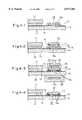
- FIGS. 1-1 to 1-4are sectional views, similar to FIG. 6, showing respective steps in the method for mounting a semiconductor chip according to the first embodiment of the invention
- FIG. 2is a plan view showing the condition of air bubbles generated in an anisotropic conductive adhesive when the first embodiment of the invention is carried out;
- FIG. 3is a diagram showing variation with time of the value of contact resistance in a reliability test run on samples prepared by a conventional mounting method and the mounting method according to the invention, respectively;
- FIGS. 4-1 to 4-4are sectional views, similar to FIG. 6, showing respective steps in the method for mounting a semiconductor chip according to a second embodiment of the invention
- FIG. 5is a plan view of a liquid crystal display to which the method for mounting the semiconductor chip according to the invention is applied;
- FIG. 6is a partially enlarged sectional view of the liquid crystal display taken along the line A--A of FIG. 5;
- FIGS. 7-1 to 7-4are sectional views, similar to FIG. 6, showing respective steps in a conventional mounting method for a semiconductor chip
- FIG. 8is a plan view showing the condition of air bubbles generated in an anisotropic conductive adhesive when the conventional mounting method for the semiconductor chip is carried out;
- FIG. 9is a diagram showing a relationship between temperature and an amount of thermal expansion of a borosilicate glass substrate and a semiconductor chip, respectively;
- FIG. 10is a diagram showing a relationship between various temperatures of the borosilicate glass substrate and thermal strain of the semiconductor chip heated to 250° C;
- FIG. 11is a sectional view of an anisotropic conductive film as an example of the anisotropic conductive adhesive.
- FIG. 12is an enlarged and partially cutaway perspective view of an electrically conductive particle contained in the anisotropic conductive film shown in FIG. 11.
- FIGS. 1-1 to 1-4are sectional views, similar to FIGS. 7-1 to 7-4, showing respective steps of a method for mounting a semiconductor chip according to the first embodiment of the invention, and parts corresponding to those in FIGS. 7-1 to 7-4 are denoted by the same reference numerals.
- an anisotropic conductive adhesive 18is disposed on portions of blank spaces 16 of a second substrate 12, (hereinafter referred to merely as a substrate), making up a circuit board of the liquid crystal panel cell, where a semiconductor chip 13 is to be mounted.
- the anisotropic conductive adhesive 18may be disposed by bonding the anisotropic conductive film (ACF) shown in FIG. 11 onto the substrate so as to be transferred. However, it may also be disposed by printing the same in paste-like form, or by applying the same thereto, using a dispenser robot with the use of a heating head, heated to a temperature in the range of 80 to 100° C.
- ACFanisotropic conductive film
- the anisotropic conductive adhesive 18has a thickness in the range of 20 to 100 ⁇ m, and is transferred to a region as large in size as the semiconductor chip 13 to be mounted, or a region larger in size by about 2 mm than the geometry of the semiconductor chip 13.
- preheatingis applied to the under surface of the substrate 12 with the anisotropic conductive adhesive 18 disposed thereon by use of a heating jig 20.
- the preheatingis applied to a temperature ranging from 100° C. to 120° C., lower than the hardening temperature of the anisotropic conductive adhesive 18, for a duration of 5 to 10 seconds.
- the heating jig 20 made of stainless steelis provided with a heater 20a built therein, and is positioned such that the region on the substrate 12, where the semiconductor chip 13 is to be mounted, can be entirely heated.
- Step 3 thereafter, the semiconductor chip 13is mounted on the substrate 12 via the anisotropic conductive adhesive 18 after aligning bump electrodes 14 formed on the semiconductor chip 13 with wiring patterns 15 formed of a transparent electrode film such as an indium tin oxide (ITO) film, tin oxide film, or the like.
- a transparent electrode filmsuch as an indium tin oxide (ITO) film, tin oxide film, or the like.
- Step 4the semiconductor chip 13 is thermally press-bonded to the glass substrate by applying pressure as well as heat with the use of a heating and pressing jig 19 provided with a heater 19a built therein, thereby hardening the anisotropic conductive adhesive 18.
- the thermal press-bondingis applied at a temperature in the range of 150 to 260° C., preferably in the range of 180 to 200° C., and at a pressure in the range of 3 to 20 kg.
- the pressurecan be applied by a driving force of an air cylinder or a motor.
- the semiconductor chip 13is bonded to the substrate 12, and a plurality of electrically conductive particles 18a are clamped between the respective bump electrodes 14 of the semiconductor chip 13 and the respective wiring patterns 15 formed on the substrate 12, thereby rendering the respective bump electrodes 14 electrically continuous with the respective wiring patterns 15.
- Volatile constituents contained in the anisotropic conductive adhesive 18are evaporated, and air involved in air bubbles is removed therefrom by preheating the substrate with the anisotropic conductive adhesive 18 disposed thereon prior to fully hardening the anisotropic conductive adhesive 18 so that as shown in FIG. 2, there occur very few air bubbles 21 when the anisotropic conductive adhesive 18 is hardened.
- adhesive resin of the anisotropic conductive adhesive 18is more densely filled between the substrate 12 and the semiconductor chip 13 as compared with the case of the conventional mounting method wherein a multitude of air bubbles are formed, thereby increasing adhesive strength, and strengthening the force holding the electrically conductive particles 18a clamped between the bump electrodes 14 and wiring patterns 15. Consequently, contact resistance values become lower and more stable.
- substrateswere prepared by bonding the anisotropic conductive adhesive to glass substrates with ITO wiring patterns formed thereon so as to be able to measure contact resistance values.
- the semiconductor chipwas heated to about 180° C. for a duration of about 20 seconds, thereby hardening the adhesive.
- the position of the semiconductor chipwas aligned on the glass substrate, and heated to about 180° C. for a duration of about 20 seconds, thereby hardening the adhesive.
- FIG. 3is a diagram (graph) showing variation in value of contact resistance between bump electrodes of the semiconductor chip and wiring patterns formed on the substrates as measured during the durability tests with reference to the samples prepared by the conventional mounting method and the mounting method according to the invention, respectively.
- the contact resistance value of the sample prepared by the conventional mounting methodis found to be about 32 ⁇ , indicating a considerable increase from the initial contact resistance value (about 5 ⁇ ) while that of the sample prepared by the method according to the invention is found to be about 10 ⁇ , indicating only a small increase from the initial contact resistance value (about 2 ⁇ ).
- the resultsshow that the method for mounting the semiconductor chip according to the invention is capable of keeping the contact resistance value at a lower level for a long time than that of the conventional method for mounting the semiconductor chip.
- FIGS. 4-1 to 4-4are sectional views, similar to FIGS. 7-1 to 7-4 and to 1-4, showing respective steps of a method for mounting a semiconductor chip according to the second embodiment of the invention, and corresponds to the sectional view taken along the line A--A of FIG. 5.
- FIGS. 4-1 to 4-4parts corresponding to those in FIGS. 7-1 to 7-4 and 1-1 to 1-4, respectively, are denoted by the same reference numerals.
- Steps 1 and 2 shown in FIGS. 4-1 and 4-2are the same as Steps 1 and 2 of the conventional mounting method shown in FIGS. 7-1 and 7-2.
- an anisotropic conductive adhesive 18is disposed by means of transferal or the like on portions of blank spaces 16 of a substrate 12, (hereinafter referred to merely as a substrate), making up a circuit board of a liquid crystal panel cell, where a semiconductor chip 13 is to be mounted.
- Step 2after aligning bump electrodes 14 of the semiconductor chip 13 with wiring patterns 15 formed on the substrate 12, facing the bump electrodes 14, the semiconductor chip 13 is disposed on the substrate 12, with the anisotropic conductive adhesive 18 interposed therebetween.
- Step 3which is a step unique to this embodiment of the invention, when thermally press-bonding the semiconductor chip 13 to the substrate 12 by applying pressure as well as heat, and hardening the anisotropic conductive adhesive 18 by use of a heating and pressing jig 19 provided with a heater 19a built therein, the under surface (a surface on the opposite side of the surface with the semiconductor chip 13 disposed thereon) of the substrate 12 is simultaneously heated by a heating jig 20 with a heater 20a built therein.
- the temperature at which heating is applied from below, as described above,is lower than that to which the semiconductor chip 13 is heated, and a specific example will be described hereinafter.
- Step 4upon hardening of the anisotropic conductive adhesive 18, adhesion of the semiconductor chip 13 onto the substrate 12 is accomplished, rendering the bump electrodes 14 electrically continuous with the wiring patterns 15 by the effect of the electrically conductive particles 18a clamped between the bump electrodes 14 of the semiconductor chip 13 and the wiring patterns 15.
- the semiconductor chip 13is heated to reach a temperature in the range of 150 to 260° C., preferably, in the range of 180 to 240° C., and a pressure in the range of 1 to 30 kg is applied for a duration of 5 to 10 seconds.
- the temperature of the substrate 12rises to only around 100° C.
- the glass substrate 12which is a borosilicate glass substrate, and the semiconductor chip 13 to an identical temperature
- the glass substrate having a greater thermal expansion coefficientundergoes larger elongation than that of the semiconductor chip.
- the diagonally shaded area in FIG. 9represents the aggregate amount of discrepancy in thermal expansion between the glass substrate and the semiconductor chip. A discrepancy amounting to 0.005025 mm occurs at 250° C.
- the heating jig 20is disposed on the under surface of the substrate 12 for heating the same so as to be able to adjust the difference in temperature between the semiconductor chip 13 and the substrate 12.
- the thermal strainis reduced to nearly zero by heating the substrate 12 to about 130° C. This point is further explained hereinafter referring to numerical values.
- the elongation occurring in the glass substrate and the semiconductor chip, respectivelyis calculated as follows. If calculation is made for one half of respective members on one side only assuming that the semiconductor chip has a side 15 mm long, and elongation caused by thermal expansion occurs bisymmetrically, the elongation of the semiconductor chip 13 heated up to 250° C. is found by the following formula:
- the amount of discrepancy in thermal expansion between the glass substrate and the semiconductor chipis given as follows, enabling the thermal strain to be reduced to nearly zero:
- the thermal straincan be completely eliminated by heating the substrate 12 to about 129.1372° C.
- the glass substratemay preferably be heated to about 130° C. by use of a heating jig.
- the semiconductor chipcan be mounted without causing thermal strain by adjusting the temperature on the side of the circuit board after calculating a temperature at which thermal shrinkage of the circuit board becomes the same as that of the semiconductor chip on the basis of the thermal expansion coefficients of the materials used.
- a third embodiment of a method for mounting a semiconductor chip according to the inventioncan be carried out by combining the first embodiment with the second embodiment described in the foregoing.
- Step 3 of the method for mounting the semiconductor chip according to the first embodiment of the invention as shown in FIG. 1-3may be substituted by Step 4 of the second embodiment as illustrated in FIG. 4-4.
- Step 2the substrate 12 with the anisotropic conductive adhesive 18 disposed thereon is preheated to a temperature lower than the hardening temperature of the anisotropic conductive adhesive 18 by use of the heating jig 20, and in Step 3 of hardening the anisotropic conductive adhesive, the substrate 12 is heated from the under surface side thereof as well by use of the heating jig 20 to a temperature lower than the heating temperature to which the semiconductor chip 13 is heated by use of the heating jig 19.
- the anisotropic conductive adhesiveis heated prior to disposing the semiconductor chip on the circuit board so as to evaporate volatile constituents contained in the adhesive, and then, the semiconductor chip is mounted on and thermally press-bonded to the substrate, thereby inhibiting generation of air bubbles when hardening the anisotropic conductive adhesive.
- Thiswill enable adhesive strength to be enhanced so that highly reliable mounting of the semiconductor chip on the circuit board can be carried out.
- the difference in elongation between the circuit board and the semiconductor chip due to the difference in thermal expansion coefficient therebetweencan be eliminated by thermally press-bonding the semiconductor chip while heating the circuit board from the side of the under surface thereof so that an excellent connection without thermal strain can be attained when the temperatures of the circuit board and the semiconductor chip return to room temperature after completion of the step of hardening the anisotropic conductive adhesive by heating.
Landscapes
- Engineering & Computer Science (AREA)
- Computer Hardware Design (AREA)
- Microelectronics & Electronic Packaging (AREA)
- Power Engineering (AREA)
- Chemical & Material Sciences (AREA)
- Organic Chemistry (AREA)
- Wire Bonding (AREA)
- Electric Connection Of Electric Components To Printed Circuits (AREA)
Abstract
Description
1. Field of the Invention
The invention relates to a method for mounting a semiconductor chip provided with bump electrodes on a circuit board with wiring patterns formed thereon, and particularly, to a method for fixing a semiconductor chip to the circuit board with the use of an anisotropic conductive adhesive while connecting the bump electrodes of the semiconductor chip to the wiring patterns on the circuit board.
2. Description of the Related Art
A method for mounting a semiconductor chip (device) for driving liquid crystals on, for example, a glass substrate of a liquid crystal panel cell by use of an anisotropic conductive adhesive has already been put to commercial use.
Such a conventional method for mounting the semiconductor chip is described hereinafter with reference to FIG. 5 showing a plan view, FIG. 6 showing a sectional view taken along the line A--A of FIG. 5, and FIGS. 7-1 to 7-4 sectional views similar to FIG. 6, showing respective steps in the method for mounting the semiconductor chip.
As shown in FIG. 5, a liquid crystal display has a construction whereinwiring patterns 15 for outputting signals to the display thereof are formed onblank spaces 16 of afirst substrate 11 and asecond substrate 12, respectively, making up a circuit board of a liquid crystal panel cell, so that a plurality ofsemiconductor chips 13 for driving liquid crystals can be mounted on thewiring patterns 15.
As material for thewiring patterns 15, a transparent and electrically conductive film such as an indium tin oxide (ITO) film, tin oxide film, or the like, is used.
As shown in FIG. 6, thesemiconductor chip 13 to be mounted on theblank spaces 16 of thesubstrates wiring patterns 15 formed thereon, is adhered thereto, respectively, by means of an anisotropicconductive adhesive 18.
The anisotropicconductive adhesive 18 is an insulating epoxy-based adhesive mixed with metal particles of silver, solder, or the like, 5 to 10 μm in grain size, or mixed with electricallyconductive particles 18a such as plastic particles rendered electrically conductive by plating the surface thereof with gold, or the like.
Thewiring patterns 15 are rendered electrically continuous withbump electrodes 14 provided on thesemiconductor chip 13, opposite to thewiring patterns 15, respectively, by interposing therebetween the electricallyconductive particles 18a contained in the anisotropicconductive adhesive 18.
An anisotropic conductive film (ACF) 180 sandwiched between abase film 181 and acover film 182 as shown in FIG. 11 is available as the anisotropicconductive adhesive 18 in the form of a film. The ACF 180 is an adhesive layer composed of thermosetting epoxy resin, containing a plurality of the electricallyconductive particles 18a.
As shown in FIG. 12, the electricallyconductive particles 18a are spherical in shape and on the order of 5 μm in diameter. A gold plated layer 18a2 is formed on the surface of a plastic core 18a1 thereof, and the surface of the gold plated layer 18a2 is further covered with an insulation layer 18a3.
Accordingly, the electricallyconductive particles 18a are insulated from each other within the ACF 180. The ACF 180 sandwiched depthwise between electrically conductive members, when heated and compressed, becomes electrically conductive due to destruction of the insulation layer 18a3 of the electricallyconductive particles 18a. However, conduction of electricity does not occur in the lateral direction of theACF 180 because the insulation layer 18a3 of the electricallyconductive particles 18a present in lateral regions is not destroyed.
Steps in the conventional method for mounting a semiconductor chip are described hereinafter with reference to FIGS. 7-1 to 7-4.
InStep 1, as shown in FIG. 7-1 the anisotropicconductive adhesive 18 is transferred to and disposed on portions of theblank spaces 16 of thesubstrate 12, where thesemiconductor chip 13 is to be mounted.
For example, after thecover film 182 shown in FIG. 11 is peeled off and the ACF 180 is pasted on thesubstrate 12, thebase film 181 is peeled off.
Subsequently, inStep 2, as shown in FIG. 7-2, after aligning thebump electrodes 14 of thesemiconductor chip 13 with thewiring patterns 15 facing thebump electrodes 14, thesemiconductor chip 13 is disposed on thesubstrate 12, with the anisotropicconductive adhesive 18 interposed therebetween.
InStep 3 as shown in FIG. 7-3 thereafter, by use of a heating and pressingjig 19 provided with aheater 19a built therein, thesemiconductor chip 13 is thermally press-bonded to thesecond substrate 12 by heating while applying pressure, hardening the anisotropicconductive adhesive 18.
In Step 4 as shown in FIG. 7-4 with the anisotropicconductive adhesive 18 hardened in the preceding step, thesemiconductor chip 13 is adhered to thesubstrate 12, thereby clamping a plurality of the electricallyconductive particles 18a between thebump electrodes 14 of thesemiconductor chip 13 and thewiring patterns 15 over thesubstrate 12, opposite thereto, respectively, with the result that therespective bump electrodes 14 are rendered electrically continuous with therespective wiring patterns 15.
As the anisotropicconductive adhesive 18 is an insulating epoxy-based adhesive with the electricallyconductive particles 18a dispersed therein, or as with the case ofACF 180 shown in FIGS. 11 and 12, the spherical surface of the respective electricallyconductive particles 18a is covered with the insulation layer 18a3, the electricallyconductive particles 18a, other than those clamped between thebump electrodes 14 and thewiring patterns 15, are insulated from each other. Accordingly, there is no possibility of short-circuit occurring between theindividual bump electrodes 14 themselves, or between theindependent wiling patterns 15.
In the conventional method for mounting the semiconductor chip described above, however, air bubbles involving volatile constituents (diluent, moisture, and the like) contained in the anisotropicconductive adhesive 18, air, and the like are formed between thesemiconductor chip 13 and thesubstrate 12 when hardening the anisotropicconductive adhesive 18 by heating.
Thus, as shown in FIG. 8,air bubbles 21 are formed on the surface of the epoxy-based adhesive material of the anisotropicconductive adhesive 18 between thesemiconductor chip 13 andsubstrate 12, where adhesion is to take place.
As a result, the epoxy based adhesive material of the anisotropicconductive adhesive 18 cannot be fully filled between thesemiconductor chip 13 andsubstrate 12, impairing adhesion strength. This has caused a problem of electrical continuity between thebump electrodes 14 andwiring patterns 15 being disrupted at times due to exfoliation of thesemiconductor chip 13 from thesubstrate 12.
Further, after thesemiconductor chip 13 is press-bonded to thesubstrate 12 by heating, thesemiconductor chip 13 andsubstrate 12 will be found in a condition wherein thermal strain occurs therebetween.
In comparing the thermal expansion coefficient of, for example, a borosilicate glass substrate often used for thesubstrate 12 of the liquid crystal panel cell with that of thesemiconductor chip 13 composed primarily of silicon, the glass substrate has a higher thermal expansion coefficient. Accordingly, when the temperature of the anisotropicconductive adhesive 18 declines to room temperature after thesemiconductor chip 13 has been press-bonded to thesubstrate 12 by heating and the anisotropicconductive adhesive 18 has been hardened, the difference in thermal expansion coefficient between thesemiconductor chip 13 andsubstrate 12 causes a difference in shrinkage to occur between materials making up respective members.
FIG. 9 shows the relationship between amounts of thermal expansion and heating temperatures with respect to a borosilicate glass substrate and a semiconductor chip. The thermal expansion coefficient of the borosilicate glass substrate, α glass, is expressed as follows:
α glass=51×10.sup.-7 /°C.
On the other hand, the thermal expansion coefficient of the semiconductor chip composed primarily of silicon, α IC, is expressed as follows:
α IC=24.2×10.sup.-7 /°C.
That is, the first andsecond substrates semiconductor chip 13.
When a temperature difference of ΔT is applied to amaterial 1 meter long and having thermal expansion coefficient α, elongation L (m) of the material is generally found by the following formula:
L=α×1×ΔT.
Assuming that the anisotropicconductive adhesive 18 is cured at 210° C., thesemiconductor chip 13 needs to be heated to a temperature on the order of 250° C. Further, the duration of press-bonding is in the range of 5 to 10 seconds.
With the duration of press-bonding ranging from 5 to 10 seconds, the temperature on the side of thesubstrate 12 rises to only around 100° C.
The elongation occurring to the substrate (glass substrate) 12 and thesemiconductor chip 13, respectively, is calculated hereinafter assuming that room temperature is 20° C.
Assuming further that a semiconductor chip has aside 15 mm long, and the elongation caused by thermal expansion occurs bisymmetrically, calculation of the elongation is made for one half of respective members on one side only.
Then, the elongation of thesubstrate 12 is found by the following formula:
(15 mm÷2)×51×10.sup.-7 ×(100° C.-20° C.)=0.0030600 mm.
On the other hand, the elongation of the semiconductor chip is found by the following formula:
(15 mm÷2)×24.2×10.sup.-7 ×(250° C.-20° C.)=0.0041745 mm.
Accordingly, the discrepancy in the elongation between thesubstrate 12 and thesemiconductor chip 13 amounts to the value given below, indicating that thesemiconductor chip 13 is further elongated by about 1 μm:
0.0041745-0.0030600 mm=0.0011145 mm.
If respective materials are left as they are after the temperatures thereof are allowed to come down to room temperature at 20° C. with such a difference in elongation therebetween as described remaining, thermal strain will occur on bonded surfaces of thesemiconductor chip 13 and substrate 12 (more specifically, between thebump electrodes 14 and thewiring patterns 15, and between thesemiconductor chip 13 and substrate 12) due to a difference in shrinkage therebetween, causing a problem of exfoliation.
FIG. 10 shows the relationship between temperatures of the borosilicate glass substrate and strain in the semiconductor chip for driving liquid crystals when heated to 250° C. in relation to the glass substrate.
The invention has been developed in order to solve such problems described above as encountered in carrying out the conventional method for mounting a semiconductor chip using an anisotropic conductive adhesive. More specifically, it is an object of the invention to provide a highly reliable method for mounting a semiconductor chip on a circuit board whereby generation of air bubbles between the semiconductor chip and circuit board is inhibited, and exfoliation of the semiconductor chip from the circuit board and poor electrical continuity between bump electrodes and wiring patterns are prevented by eliminating the difference in elongation between the semiconductor chip and circuit board after thermal press-bonding of the former to the latter.
To this end, in the method for mounting the semiconductor chip on the circuit board according to the invention, the circuit board with the anisotropic conductive adhesive disposed thereon is preheated to a temperature lower than the hardening temperature of the anisotropic conductive adhesive after disposing the anisotropic conductive adhesive on the circuit board, but before disposing the semiconductor chip on the circuit board.
Volatile constituents contained in the anisotropic conductive adhesive are evaporated by preheating the circuit board with the anisotropic conductive adhesive disposed thereon so that very few air bubbles are generated when the semiconductor chip is thermally press-bonded. As a result, the amount of air bubbles generated between the semiconductor chip and the circuit board is dramatically reduced, enabling highly reliable mounting of the semiconductor chip.
The invention also proposes that in a step of hardening the anisotropic conductive adhesive by thermally press-bonding the semiconductor chip to the circuit board by applying pressure as well as heat, and a surface of the circuit board on the opposite side of a surface thereof with the semiconductor chip disposed thereon, is also heated to a temperature lower than a temperature to which the semiconductor chip is heated.
The amount of thermal expansion of the circuit board can be rendered substantially equal to that of the semiconductor chip by thus adjusting the temperature of the circuit board by heating the same as well, thereby preventing thermal strain from occurring between the circuit board and the semiconductor chip when the temperatures of the circuit board and the semiconductor chip return to room temperature after thermal press-bonding.
Accordingly, exfoliation of the semiconductor chip from the circuit board and poor electrical continuity between bump electrodes and wiring patterns can be prevented, attaining highly reliable mounting.
It is thus possible to provide a reliable mounting method wherein generation of air bubbles is substantially eliminated and strain between the circuit board and the semiconductor chip is inhibited by applying both the step of preheating the circuit board with the anisotropic conductive adhesive disposed thereon to a temperature lower than the hardening temperature of the anisotropic conductive adhesive, and the step of heating the surface of the circuit board on the opposite side of the surface thereof with the semiconductor chip disposed thereon, to a temperature lower than the temperature to which the semiconductor chip is heated, during the step of hardening the anisotropic conductive adhesive.
The above and other objects, features, and advantages of the invention will be apparent from the following detailed description which is to be read in conjunction with the accompanying drawings.
FIGS. 1-1 to 1-4 are sectional views, similar to FIG. 6, showing respective steps in the method for mounting a semiconductor chip according to the first embodiment of the invention;
FIG. 2 is a plan view showing the condition of air bubbles generated in an anisotropic conductive adhesive when the first embodiment of the invention is carried out;
FIG. 3 is a diagram showing variation with time of the value of contact resistance in a reliability test run on samples prepared by a conventional mounting method and the mounting method according to the invention, respectively;
FIGS. 4-1 to 4-4 are sectional views, similar to FIG. 6, showing respective steps in the method for mounting a semiconductor chip according to a second embodiment of the invention;
FIG. 5 is a plan view of a liquid crystal display to which the method for mounting the semiconductor chip according to the invention is applied;
FIG. 6 is a partially enlarged sectional view of the liquid crystal display taken along the line A--A of FIG. 5;
FIGS. 7-1 to 7-4 are sectional views, similar to FIG. 6, showing respective steps in a conventional mounting method for a semiconductor chip;
FIG. 8 is a plan view showing the condition of air bubbles generated in an anisotropic conductive adhesive when the conventional mounting method for the semiconductor chip is carried out;
FIG. 9 is a diagram showing a relationship between temperature and an amount of thermal expansion of a borosilicate glass substrate and a semiconductor chip, respectively;
FIG. 10 is a diagram showing a relationship between various temperatures of the borosilicate glass substrate and thermal strain of the semiconductor chip heated to 250° C;
FIG. 11 is a sectional view of an anisotropic conductive film as an example of the anisotropic conductive adhesive; and
FIG. 12 is an enlarged and partially cutaway perspective view of an electrically conductive particle contained in the anisotropic conductive film shown in FIG. 11.
Preferred embodiments of the method for mounting a semiconductor chip according to the invention are described hereinafter in detail with reference to accompanying drawings.
In explaining the embodiments hereinafter, a method for mounting a semiconductor chip (device) for driving liquid crystals on a glass substrate of a liquid crystal panel cell, as with the case of the conventional method previously described with reference to FIGS. 5 to 7-4, is described by way of example.
FIGS. 1-1 to 1-4 are sectional views, similar to FIGS. 7-1 to 7-4, showing respective steps of a method for mounting a semiconductor chip according to the first embodiment of the invention, and parts corresponding to those in FIGS. 7-1 to 7-4 are denoted by the same reference numerals.
As shown in FIGS. 1-1 to 1-4, inStep 1, an anisotropic conductive adhesive 18 is disposed on portions ofblank spaces 16 of asecond substrate 12, (hereinafter referred to merely as a substrate), making up a circuit board of the liquid crystal panel cell, where asemiconductor chip 13 is to be mounted.
The anisotropic conductive adhesive 18 may be disposed by bonding the anisotropic conductive film (ACF) shown in FIG. 11 onto the substrate so as to be transferred. However, it may also be disposed by printing the same in paste-like form, or by applying the same thereto, using a dispenser robot with the use of a heating head, heated to a temperature in the range of 80 to 100° C.
The anisotropic conductive adhesive 18 has a thickness in the range of 20 to 100 μm, and is transferred to a region as large in size as thesemiconductor chip 13 to be mounted, or a region larger in size by about 2 mm than the geometry of thesemiconductor chip 13.
As shown in FIG. 1-2, inStep 2, preheating is applied to the under surface of thesubstrate 12 with the anisotropic conductive adhesive 18 disposed thereon by use of aheating jig 20. The preheating is applied to a temperature ranging from 100° C. to 120° C., lower than the hardening temperature of the anisotropic conductive adhesive 18, for a duration of 5 to 10 seconds.
Theheating jig 20 made of stainless steel is provided with aheater 20a built therein, and is positioned such that the region on thesubstrate 12, where thesemiconductor chip 13 is to be mounted, can be entirely heated.
As shown in FIG. 1-3, inStep 3 thereafter, thesemiconductor chip 13 is mounted on thesubstrate 12 via the anisotropic conductive adhesive 18 after aligningbump electrodes 14 formed on thesemiconductor chip 13 withwiring patterns 15 formed of a transparent electrode film such as an indium tin oxide (ITO) film, tin oxide film, or the like.
As shown in FIG. 1-4, in Step 4, thesemiconductor chip 13 is thermally press-bonded to the glass substrate by applying pressure as well as heat with the use of a heating andpressing jig 19 provided with aheater 19a built therein, thereby hardening the anisotropicconductive adhesive 18.
The thermal press-bonding is applied at a temperature in the range of 150 to 260° C., preferably in the range of 180 to 200° C., and at a pressure in the range of 3 to 20 kg. The pressure can be applied by a driving force of an air cylinder or a motor.
As a result of the steps described above, thesemiconductor chip 13 is bonded to thesubstrate 12, and a plurality of electricallyconductive particles 18a are clamped between therespective bump electrodes 14 of thesemiconductor chip 13 and therespective wiring patterns 15 formed on thesubstrate 12, thereby rendering therespective bump electrodes 14 electrically continuous with therespective wiring patterns 15.
Volatile constituents contained in the anisotropic conductive adhesive 18 are evaporated, and air involved in air bubbles is removed therefrom by preheating the substrate with the anisotropic conductive adhesive 18 disposed thereon prior to fully hardening the anisotropic conductive adhesive 18 so that as shown in FIG. 2, there occur very few air bubbles 21 when the anisotropic conductive adhesive 18 is hardened.
Due to the occurrence of fewer air bubbles, adhesive resin of the anisotropic conductive adhesive 18 is more densely filled between thesubstrate 12 and thesemiconductor chip 13 as compared with the case of the conventional mounting method wherein a multitude of air bubbles are formed, thereby increasing adhesive strength, and strengthening the force holding the electricallyconductive particles 18a clamped between thebump electrodes 14 andwiring patterns 15. Consequently, contact resistance values become lower and more stable.
In this connection, comparative tests were carried out to compare a case where a semiconductor chip is actually mounted on a circuit board by the conventional method with a case of mounting the same by the method according to the invention. The comparative tests and the results thereof are described hereinafter.
In the tests, substrates were prepared by bonding the anisotropic conductive adhesive to glass substrates with ITO wiring patterns formed thereon so as to be able to measure contact resistance values. In the case of testing the conventional mounting method, after aligning the position of the semiconductor chip on the substrate as it is, the semiconductor chip was heated to about 180° C. for a duration of about 20 seconds, thereby hardening the adhesive.
In the case of testing the mounting method according to the invention, after leaving a glass substrate with the anisotropic conductive adhesive bonded thereto on a hot plate heated to a temperature on the order of 100° C. for about 10 seconds, thereby evaporating volatile constituents contained in the anisotropic conductive adhesive, the position of the semiconductor chip was aligned on the glass substrate, and heated to about 180° C. for a duration of about 20 seconds, thereby hardening the adhesive.
Then, durability tests were carried out on samples prepared by the conventional mounting method and the mounting method according to the invention, respectively, wherein the samples were left in a furnace set in a high temperature and high-moisture atmosphere of 85% humidity at 85° C. for a retention time of 500 hours.
FIG. 3 is a diagram (graph) showing variation in value of contact resistance between bump electrodes of the semiconductor chip and wiring patterns formed on the substrates as measured during the durability tests with reference to the samples prepared by the conventional mounting method and the mounting method according to the invention, respectively.
As is evident from FIG. 3, the contact resistance value of the sample prepared by the conventional mounting method, after the elapse of 500 hours, is found to be about 32Ω, indicating a considerable increase from the initial contact resistance value (about 5Ω) while that of the sample prepared by the method according to the invention is found to be about 10Ω, indicating only a small increase from the initial contact resistance value (about 2Ω).
The results show that the method for mounting the semiconductor chip according to the invention is capable of keeping the contact resistance value at a lower level for a long time than that of the conventional method for mounting the semiconductor chip.
Next, a second embodiment of a method for mounting a semiconductor chip according to the invention will be described taking as an example the case of mounting a semiconductor chip for driving liquid crystals on a liquid crystal panel cell, like the case of the embodiment previously described with reference to FIGS. 5 and 6.
FIGS. 4-1 to 4-4 are sectional views, similar to FIGS. 7-1 to 7-4 and to 1-4, showing respective steps of a method for mounting a semiconductor chip according to the second embodiment of the invention, and corresponds to the sectional view taken along the line A--A of FIG. 5. In FIGS. 4-1 to 4-4, parts corresponding to those in FIGS. 7-1 to 7-4 and 1-1 to 1-4, respectively, are denoted by the same reference numerals.
In the second embodiment, Steps 1 and 2 shown in FIGS. 4-1 and 4-2 are the same asSteps
As shown in FIGS. 4-1, inStep 1, an anisotropic conductive adhesive 18 is disposed by means of transferal or the like on portions ofblank spaces 16 of asubstrate 12, (hereinafter referred to merely as a substrate), making up a circuit board of a liquid crystal panel cell, where asemiconductor chip 13 is to be mounted.
As shown in FIG. 4-2, inStep 2 after aligningbump electrodes 14 of thesemiconductor chip 13 withwiring patterns 15 formed on thesubstrate 12, facing thebump electrodes 14, thesemiconductor chip 13 is disposed on thesubstrate 12, with the anisotropic conductive adhesive 18 interposed therebetween.
As shown in FIG. 4-3, inStep 3, which is a step unique to this embodiment of the invention, when thermally press-bonding thesemiconductor chip 13 to thesubstrate 12 by applying pressure as well as heat, and hardening the anisotropic conductive adhesive 18 by use of a heating andpressing jig 19 provided with aheater 19a built therein, the under surface (a surface on the opposite side of the surface with thesemiconductor chip 13 disposed thereon) of thesubstrate 12 is simultaneously heated by aheating jig 20 with aheater 20a built therein. The temperature at which heating is applied from below, as described above, is lower than that to which thesemiconductor chip 13 is heated, and a specific example will be described hereinafter.
As shown in FIG. 4-4 in Step 4, upon hardening of the anisotropic conductive adhesive 18, adhesion of thesemiconductor chip 13 onto thesubstrate 12 is accomplished, rendering thebump electrodes 14 electrically continuous with thewiring patterns 15 by the effect of the electricallyconductive particles 18a clamped between thebump electrodes 14 of thesemiconductor chip 13 and thewiring patterns 15.
During the thermal press-bonding inStep 3, thesemiconductor chip 13 is heated to reach a temperature in the range of 150 to 260° C., preferably, in the range of 180 to 240° C., and a pressure in the range of 1 to 30 kg is applied for a duration of 5 to 10 seconds.
Meanwhile, with the duration of press-bonding ranging from 5 to 10 seconds, the temperature of thesubstrate 12 rises to only around 100° C.
As shown in FIG. 9, when heating up both thesubstrate 12, which is a borosilicate glass substrate, and thesemiconductor chip 13 to an identical temperature, the glass substrate having a greater thermal expansion coefficient undergoes larger elongation than that of the semiconductor chip. The diagonally shaded area in FIG. 9 represents the aggregate amount of discrepancy in thermal expansion between the glass substrate and the semiconductor chip. A discrepancy amounting to 0.005025 mm occurs at 250° C.
In order to eliminate such difference in elongation, theheating jig 20 is disposed on the under surface of thesubstrate 12 for heating the same so as to be able to adjust the difference in temperature between thesemiconductor chip 13 and thesubstrate 12.
Based on the diagram (graph) shown in FIG. 10, indicating the relationship between temperatures of the glass substrate and magnitude of thermal strain of thesemiconductor chip 13 heated up to 250° C., the degree to which heating of thesubstrate 12, that is, the glass substrate, must be performed to eliminate the strain when thesemiconductor chip 13 is heated up to 250° C. can be found.
The thermal strain is reduced to nearly zero by heating thesubstrate 12 to about 130° C. This point is further explained hereinafter referring to numerical values.
Assuming that room temperature is set at 20° C., the elongation occurring in the glass substrate and the semiconductor chip, respectively, is calculated as follows. If calculation is made for one half of respective members on one side only assuming that the semiconductor chip has aside 15 mm long, and elongation caused by thermal expansion occurs bisymmetrically, the elongation of thesemiconductor chip 13 heated up to 250° C. is found by the following formula:
(15 mm÷2)×24.2×10.sup.-7 ×(250° C.-20° C.)=0.0041745 mm.
In this instance, the elongation of thesubstrate 12 heated to 130° C. is found by the following formula:
(15 mm÷2)×51×10.sup.-7 ×(130° C.-20° C.)=0.0042075 mm.
Accordingly, the amount of discrepancy in thermal expansion between the glass substrate and the semiconductor chip is given as follows, enabling the thermal strain to be reduced to nearly zero:
0.0041745 mm-0.0042075 mm=0.0000330 mm.
Then, by calculation, it can be found that the thermal strain can be completely eliminated by heating thesubstrate 12 to about 129.1372° C.
It can be said from above results that when mounting a semiconductor chip for driving liquid crystals on a borosilicate glass substrate, the glass substrate may preferably be heated to about 130° C. by use of a heating jig.
Even in the case where a semiconductor chip is mounted on a circuit board composed of another material having a different thermal expansion coefficient, or in the case where another anisotropic conductive adhesive having a different curing temperature is used, the semiconductor chip can be mounted without causing thermal strain by adjusting the temperature on the side of the circuit board after calculating a temperature at which thermal shrinkage of the circuit board becomes the same as that of the semiconductor chip on the basis of the thermal expansion coefficients of the materials used.
Further, a third embodiment of a method for mounting a semiconductor chip according to the invention can be carried out by combining the first embodiment with the second embodiment described in the foregoing.
That is,Step 3 of the method for mounting the semiconductor chip according to the first embodiment of the invention as shown in FIG. 1-3 may be substituted by Step 4 of the second embodiment as illustrated in FIG. 4-4.
More specifically, inStep 2, thesubstrate 12 with the anisotropic conductive adhesive 18 disposed thereon is preheated to a temperature lower than the hardening temperature of the anisotropic conductive adhesive 18 by use of theheating jig 20, and inStep 3 of hardening the anisotropic conductive adhesive, thesubstrate 12 is heated from the under surface side thereof as well by use of theheating jig 20 to a temperature lower than the heating temperature to which thesemiconductor chip 13 is heated by use of theheating jig 19.
This will substantially eliminate generation of air bubbles between the anisotropic conductive adhesive 18 and thesemiconductor chip 13 as well as thesubstrate 12, and thermal strain between thesubstrate 12 and thesemiconductor chip 13 is also inhibited, thereby also enabling attainment of reliable mounting.
As described hereinbefore, in the method for mounting the semiconductor chip according to the invention, the anisotropic conductive adhesive is heated prior to disposing the semiconductor chip on the circuit board so as to evaporate volatile constituents contained in the adhesive, and then, the semiconductor chip is mounted on and thermally press-bonded to the substrate, thereby inhibiting generation of air bubbles when hardening the anisotropic conductive adhesive. This will enable adhesive strength to be enhanced so that highly reliable mounting of the semiconductor chip on the circuit board can be carried out.
Further, during the step of thermally press-bonding the semiconductor chip, the difference in elongation between the circuit board and the semiconductor chip due to the difference in thermal expansion coefficient therebetween can be eliminated by thermally press-bonding the semiconductor chip while heating the circuit board from the side of the under surface thereof so that an excellent connection without thermal strain can be attained when the temperatures of the circuit board and the semiconductor chip return to room temperature after completion of the step of hardening the anisotropic conductive adhesive by heating.
It is thus also possible to achieve reliable mounting of the semiconductor chip on the circuit board by applying both steps as described above.
Claims (3)
1. A method for mounting a semiconductor chip provided with bump electrodes on a circuit board with wiring patterns formed thereon;
said method for mounting the semiconductor chip comprising:
a step of disposing a thermosetting anisotropic conductive adhesive on the circuit board;
a step of preheating the circuit board with the anisotropic conductive adhesive on the circuit board to a temperature lower than the hardening temperature of the anisotropic conductive adhesive;
a step of disposing the semiconductor chip on the circuit board after the preheating step and after aligning the bump electrodes of the semiconductor chip with the wiring patterns formed on the circuit board; and
a step of hardening the thermosetting anisotropic conductive adhesive by thermally press-bonding the semiconductor chip onto the circuit board by applying pressure as well as heat to said semiconductor chip.
2. A method for mounting a semiconductor chip provided with bump electrodes on a circuit board with wiring patterns formed thereon;
said method for mounting the semiconductor chip comprising:
a step of disposing a thermosetting anisotropic conductive adhesive on the circuit board;
a step of disposing the semiconductor chip on the circuit board after aligning the bump electrodes of the semiconductor chip with the wiring patterns formed on the circuit board; and
a step of hardening the thermosetting anisotropic conductive adhesive by thermally press-bonding the semiconductor chip onto the circuit board by applying pressure as well as heat to said semiconductor chip, and by simultaneously heating a surface of the circuit board opposite said thermosetting anisotropic conductive adhesive with the semiconductor chip disposed on the circuit board to a temperature lower than a temperature to which the semiconductor chip is heated.
3. A method for mounting a semiconductor chip provided with bump electrodes on a circuit board with wiring patterns formed thereon;
said method for mounting the semiconductor chip comprising:
a step of disposing a thermosetting anisotropic conductive adhesive on the circuit board;
a step of preheating the circuit board with the thermosetting anisotropic conductive adhesive disposed thereon to a temperature lower than the hardening temperature of the thermosetting anisotropic conductive adhesive;
a step of disposing the semiconductor chip on the circuit board after aligning the bump electrodes of the semiconductor chip with the wiring patterns formed on the circuit board; and
a step of hardening the thermosetting anisotropic conductive adhesive by thermally press-bonding the semiconductor chip onto the circuit board by applying pressure as well as heat to said semiconductor chip, and by simultaneously heating a surface of the circuit board opposite said thermosetting anisotropic conductive adhesive with the semiconductor chip disposed on the circuit board to a temperature lower than a temperature to which the semiconductor chip is heated.
Applications Claiming Priority (4)
| Application Number | Priority Date | Filing Date | Title |
|---|---|---|---|
| JP11921697 | 1997-05-09 | ||
| JP9-119216 | 1997-05-09 | ||
| JP9-190868 | 1997-07-16 | ||
| JP19086897 | 1997-07-16 |
Publications (1)
| Publication Number | Publication Date |
|---|---|
| US6077382Atrue US6077382A (en) | 2000-06-20 |
Family
ID=26456995
Family Applications (1)
| Application Number | Title | Priority Date | Filing Date |
|---|---|---|---|
| US09/074,425Expired - LifetimeUS6077382A (en) | 1997-05-09 | 1998-05-08 | Mounting method of semiconductor chip |
Country Status (1)
| Country | Link |
|---|---|
| US (1) | US6077382A (en) |
Cited By (40)
| Publication number | Priority date | Publication date | Assignee | Title |
|---|---|---|---|---|
| US6281567B1 (en)* | 1998-06-16 | 2001-08-28 | Shinko Electric Industries Co., Ltd. | Substrate for mounting semiconductor chip with parallel conductive lines |
| US6312551B1 (en)* | 1998-06-17 | 2001-11-06 | Shinko Electric Industries Co., Ltd. | Method for mounting semiconductor chip onto circuit board |
| US6315856B1 (en)* | 1998-03-19 | 2001-11-13 | Kabushiki Kaisha Toshiba | Method of mounting electronic component |
| US20020053747A1 (en)* | 1998-07-01 | 2002-05-09 | Nobuaki Hashimoto | Semiconductor device and method of manufacture thereof, circuit board and electronic instrument |
| WO2002049093A1 (en)* | 2000-12-11 | 2002-06-20 | Rafsec Oy | A smart label web and a method for its manufacture |
| US6452111B1 (en)* | 2000-10-16 | 2002-09-17 | Sony Chemicals Corp. | Adhesives and adhesive films |
| US6467139B1 (en)* | 1998-08-03 | 2002-10-22 | Nec Corporation | Mounting structure and mounting method for surface acoustic wave element |
| US20020164837A1 (en)* | 2000-04-25 | 2002-11-07 | Fujitsu Limited | Method of mounting semiconductor chip |
| US20030025213A1 (en)* | 2000-04-19 | 2003-02-06 | Hermann Schmid | Device for attaching a semiconductor chip to a chip carrier |
| US20030029540A1 (en)* | 2000-01-17 | 2003-02-13 | Rafsec Oy | Method for the manufacture of a smart label inlet web, and a smart label inlet web |
| US20030052077A1 (en)* | 2000-03-31 | 2003-03-20 | Rafsec Oy | Method for forming a product sensor, and a product sensor |
| US20030121986A1 (en)* | 2000-06-06 | 2003-07-03 | Rafsec Oy | Method and an apparatus for manufacturing a smart label inlet web |
| US20030127525A1 (en)* | 2000-06-06 | 2003-07-10 | Rafsec Oy | Smart card web and a method for its manufacture |
| US20030178132A1 (en)* | 2002-03-25 | 2003-09-25 | Sony Chemicals Corp. | Method for manufacturing connection structure |
| WO2003094222A1 (en)* | 2002-04-30 | 2003-11-13 | Toray Engineering Co., Ltd. | Bonding method and bonding device |
| US6666947B2 (en)* | 2001-01-31 | 2003-12-23 | Hewlett-Packard Development Company, L.P. | Method for producing an inkjet printhead element; and an inkjet printhead element |
| US20030235939A1 (en)* | 2002-06-25 | 2003-12-25 | Hisao Takemura | Method and apparatus for manufacturing semiconductor apparatus |
| US20040005754A1 (en)* | 2000-11-20 | 2004-01-08 | Rafsec Oy | Method for attaching an integrated circuit on a silicon chip to a smart label |
| US20040079464A1 (en)* | 2001-02-26 | 2004-04-29 | Hiroyuki Kumakura | Manufacturing method for electric device |
| US20040109282A1 (en)* | 2002-12-04 | 2004-06-10 | Li Kwei Chung | Flip-chip sub-assembly, methods of making same and device including same |
| US6767763B1 (en)* | 1999-11-04 | 2004-07-27 | Seiko Epson Corporation | Component mounting method and method of producing electro-optical device |
| US6776859B1 (en)* | 2000-11-27 | 2004-08-17 | Saturn Electronics & Engineering, Inc. | Anisotropic bonding system and method using dynamic feedback |
| US20040169586A1 (en)* | 2001-05-31 | 2004-09-02 | Rafsac Oy | Smart label and a smart label web |
| US20040216839A1 (en)* | 2002-02-22 | 2004-11-04 | Satoshi Yamamoto | Method of adhesion and adhesion apparatus |
| US20050025943A1 (en)* | 2001-07-04 | 2005-02-03 | Anu Krappe | Injection moulded product and a method for its manufacture |
| US20050087607A1 (en)* | 2001-12-21 | 2005-04-28 | Samuli Stromberg | Smart label web and a method for its manufacture |
| US6889418B2 (en)* | 1998-11-24 | 2005-05-10 | Fujitsu Limited | Method of processing magnetic head |
| US20050275099A1 (en)* | 2004-06-09 | 2005-12-15 | Daijiro Takano | Semiconductor apparatus and method of manufacturing semiconductor apparatus |
| WO2008081969A1 (en)* | 2006-12-28 | 2008-07-10 | Panasonic Corporation | Connecting method of electronic component |
| US20090115611A1 (en)* | 2007-11-07 | 2009-05-07 | Fujitsu Limited | Manufacturing method for rfid tag |
| US20100038762A1 (en)* | 2007-02-16 | 2010-02-18 | Sumitomo Bakelite Co., Ltd. | Circuit board manufacturing method, semiconductor manufacturing apparatus, circuit board and semiconductor device |
| US20100230141A1 (en)* | 2009-03-13 | 2010-09-16 | Sumitomo Electric Industries, Ltd. | Structure of connecting printed wiring boards, method of connecting printed wiring boards, and adhesive having anisotropic conductivity |
| CN101840873A (en)* | 2009-03-19 | 2010-09-22 | 上海中卡智能卡有限公司 | Method based on flip chip process for connecting chip and antenna |
| US20110073357A1 (en)* | 2008-06-02 | 2011-03-31 | Nxp B.V. | Electronic device and method of manufacturing an electronic device |
| US20110189824A1 (en)* | 2008-06-02 | 2011-08-04 | Nxp B.V. | Method for manufacturing an electronic device |
| US20120217287A1 (en)* | 2011-02-28 | 2012-08-30 | International Business Machines Corporation | Flip chip assembly method employing post-contact differential heating |
| US20160280969A1 (en)* | 2013-07-29 | 2016-09-29 | Dexerials Corporation | Method for manufacturing electrically conductive adhesive film, electrically conductive adhesive film, and method for manufacturing connector |
| US9975194B2 (en)* | 2013-09-17 | 2018-05-22 | Abb Schweiz Ag | Method for ultrasonic welding with particles trapping |
| US20180164171A1 (en)* | 2016-12-14 | 2018-06-14 | Samsung Electronics Co., Ltd. | Method of correcting estimated force of bonding apparatus |
| CN111987013A (en)* | 2019-05-22 | 2020-11-24 | 三星显示有限公司 | Flexible circuit film bonding apparatus and method of bonding flexible circuit film using the same |
Citations (8)
| Publication number | Priority date | Publication date | Assignee | Title |
|---|---|---|---|---|
| US4749120A (en)* | 1986-12-18 | 1988-06-07 | Matsushita Electric Industrial Co., Ltd. | Method of connecting a semiconductor device to a wiring board |
| US5148266A (en)* | 1990-09-24 | 1992-09-15 | Ist Associates, Inc. | Semiconductor chip assemblies having interposer and flexible lead |
| US5232532A (en)* | 1991-05-27 | 1993-08-03 | Sony Corporation | Chip device bonding machine |
| US5283947A (en)* | 1992-02-10 | 1994-02-08 | Matsushita Electric Industrial Co., Inc. | Method of mounting electronic components on a circuit board |
| JPH0766225A (en)* | 1993-08-25 | 1995-03-10 | Nec Corp | Method and apparatus for manufacture of semiconductor device |
| US5628111A (en)* | 1994-03-02 | 1997-05-13 | Kabushiki Kaisha Toshiba | Methods of fabricating of semiconductor package and mounting of semiconductor device |
| US5802712A (en)* | 1995-02-23 | 1998-09-08 | Matsushita Electric Industrial Co., Ltd. | Electronic device mounting method |
| US5843251A (en)* | 1989-03-09 | 1998-12-01 | Hitachi Chemical Co., Ltd. | Process for connecting circuits and adhesive film used therefor |
- 1998
- 1998-05-08USUS09/074,425patent/US6077382A/ennot_activeExpired - Lifetime
Patent Citations (8)
| Publication number | Priority date | Publication date | Assignee | Title |
|---|---|---|---|---|
| US4749120A (en)* | 1986-12-18 | 1988-06-07 | Matsushita Electric Industrial Co., Ltd. | Method of connecting a semiconductor device to a wiring board |
| US5843251A (en)* | 1989-03-09 | 1998-12-01 | Hitachi Chemical Co., Ltd. | Process for connecting circuits and adhesive film used therefor |
| US5148266A (en)* | 1990-09-24 | 1992-09-15 | Ist Associates, Inc. | Semiconductor chip assemblies having interposer and flexible lead |
| US5232532A (en)* | 1991-05-27 | 1993-08-03 | Sony Corporation | Chip device bonding machine |
| US5283947A (en)* | 1992-02-10 | 1994-02-08 | Matsushita Electric Industrial Co., Inc. | Method of mounting electronic components on a circuit board |
| JPH0766225A (en)* | 1993-08-25 | 1995-03-10 | Nec Corp | Method and apparatus for manufacture of semiconductor device |
| US5628111A (en)* | 1994-03-02 | 1997-05-13 | Kabushiki Kaisha Toshiba | Methods of fabricating of semiconductor package and mounting of semiconductor device |
| US5802712A (en)* | 1995-02-23 | 1998-09-08 | Matsushita Electric Industrial Co., Ltd. | Electronic device mounting method |
Cited By (83)
| Publication number | Priority date | Publication date | Assignee | Title |
|---|---|---|---|---|
| US6315856B1 (en)* | 1998-03-19 | 2001-11-13 | Kabushiki Kaisha Toshiba | Method of mounting electronic component |
| US6281567B1 (en)* | 1998-06-16 | 2001-08-28 | Shinko Electric Industries Co., Ltd. | Substrate for mounting semiconductor chip with parallel conductive lines |
| US6312551B1 (en)* | 1998-06-17 | 2001-11-06 | Shinko Electric Industries Co., Ltd. | Method for mounting semiconductor chip onto circuit board |
| US20060099739A1 (en)* | 1998-07-01 | 2006-05-11 | Seiko Epson Corporation | Semiconductor device and method of manufacture thereof, circuit board and electronic instrument |
| US6972381B2 (en) | 1998-07-01 | 2005-12-06 | Seiko Epson Corporation | Semiconductor device and method of manufacture thereof, circuit board and electronic instrument |
| US7198984B2 (en) | 1998-07-01 | 2007-04-03 | Seiko Epson Corporation | Semiconductor device and method of manufacture thereof, circuit board and electronic instrument |
| US6462284B1 (en)* | 1998-07-01 | 2002-10-08 | Seiko Epson Corporation | Semiconductor device and method of manufacture thereof |
| US7560819B2 (en) | 1998-07-01 | 2009-07-14 | Seiko Epson Corporation | Semiconductor device and method of manufacture thereof, circuit board and electronic instrument |
| US20060172460A1 (en)* | 1998-07-01 | 2006-08-03 | Seiko Epson Corporation | Semiconductor device and method of manufacture thereof, circuit board and electronic instrument |
| US20020185747A1 (en)* | 1998-07-01 | 2002-12-12 | Seiko Epson Corporation | Semiconductor device and method of manufacture thereof, circuit board and electronic instrument |
| US7868466B2 (en) | 1998-07-01 | 2011-01-11 | Seiko Epson Corporation | Semiconductor device and method of manufacture thereof, circuit board and electronic instrument |
| US6995476B2 (en)* | 1998-07-01 | 2006-02-07 | Seiko Epson Corporation | Semiconductor device, circuit board and electronic instrument that include an adhesive with conductive particles therein |
| US20070132099A1 (en)* | 1998-07-01 | 2007-06-14 | Seiko Epson Corporation | Semiconductor device and method of manufacture thereof, circuit board and electronic instrument |
| US20020053747A1 (en)* | 1998-07-01 | 2002-05-09 | Nobuaki Hashimoto | Semiconductor device and method of manufacture thereof, circuit board and electronic instrument |
| US20080128921A1 (en)* | 1998-07-01 | 2008-06-05 | Seiko Epson Corporation | Semiconductor device and method of manufacture thereof, circuit board and electronic instrument |
| US6763994B2 (en) | 1998-07-01 | 2004-07-20 | Nobuaki Hashimoto | Semiconductor device and method of manufacture thereof, circuit board and electronic instrument |
| US20040256739A1 (en)* | 1998-07-01 | 2004-12-23 | Seiko Epson Corporation | Semiconductor device and method of manufacture thereof, circuit board and electronic instrument |
| US7332371B2 (en) | 1998-07-01 | 2008-02-19 | Seiko Epson Corporation | Semiconductor device and method of manufacture thereof, circuit board and electronic instrument |
| US6467139B1 (en)* | 1998-08-03 | 2002-10-22 | Nec Corporation | Mounting structure and mounting method for surface acoustic wave element |
| US6889418B2 (en)* | 1998-11-24 | 2005-05-10 | Fujitsu Limited | Method of processing magnetic head |
| US6767763B1 (en)* | 1999-11-04 | 2004-07-27 | Seiko Epson Corporation | Component mounting method and method of producing electro-optical device |
| US20030029540A1 (en)* | 2000-01-17 | 2003-02-13 | Rafsec Oy | Method for the manufacture of a smart label inlet web, and a smart label inlet web |
| US20030052077A1 (en)* | 2000-03-31 | 2003-03-20 | Rafsec Oy | Method for forming a product sensor, and a product sensor |
| US6951621B2 (en) | 2000-03-31 | 2005-10-04 | Rafsec Oy | Method for forming a product sensor, and a product sensor |
| US6559523B2 (en)* | 2000-04-19 | 2003-05-06 | Texas Instruments Incorporated | Device for attaching a semiconductor chip to a chip carrier |
| US20030025213A1 (en)* | 2000-04-19 | 2003-02-06 | Hermann Schmid | Device for attaching a semiconductor chip to a chip carrier |
| US20020164837A1 (en)* | 2000-04-25 | 2002-11-07 | Fujitsu Limited | Method of mounting semiconductor chip |
| US7394163B2 (en)* | 2000-04-25 | 2008-07-01 | Fujitsu Limited | Method of mounting semiconductor chip |
| US20030127525A1 (en)* | 2000-06-06 | 2003-07-10 | Rafsec Oy | Smart card web and a method for its manufacture |
| US20030121986A1 (en)* | 2000-06-06 | 2003-07-03 | Rafsec Oy | Method and an apparatus for manufacturing a smart label inlet web |
| US6452111B1 (en)* | 2000-10-16 | 2002-09-17 | Sony Chemicals Corp. | Adhesives and adhesive films |
| US20040005754A1 (en)* | 2000-11-20 | 2004-01-08 | Rafsec Oy | Method for attaching an integrated circuit on a silicon chip to a smart label |
| US6776859B1 (en)* | 2000-11-27 | 2004-08-17 | Saturn Electronics & Engineering, Inc. | Anisotropic bonding system and method using dynamic feedback |
| WO2002049093A1 (en)* | 2000-12-11 | 2002-06-20 | Rafsec Oy | A smart label web and a method for its manufacture |
| GB2388250B (en)* | 2000-12-11 | 2005-03-09 | Rafsec Oy | A smart label web and a method for its manufacture |
| GB2388250A (en)* | 2000-12-11 | 2003-11-05 | Rafsec Oy | A smart label web and a method for its manufacture |
| US7244332B2 (en) | 2000-12-11 | 2007-07-17 | Rafsec Oy | Smart label web and a method for its manufacture |
| US20040004295A1 (en)* | 2000-12-11 | 2004-01-08 | Rafsec Oy | Smart label web and a method for its manufacture |
| US6666947B2 (en)* | 2001-01-31 | 2003-12-23 | Hewlett-Packard Development Company, L.P. | Method for producing an inkjet printhead element; and an inkjet printhead element |
| US7341642B2 (en)* | 2001-02-26 | 2008-03-11 | Sony Corporation | Manufacturing method for electric device |
| US20040079464A1 (en)* | 2001-02-26 | 2004-04-29 | Hiroyuki Kumakura | Manufacturing method for electric device |
| US7066393B2 (en) | 2001-05-31 | 2006-06-27 | Rafsec Oy | Smart label and a smart label web |
| US20040169586A1 (en)* | 2001-05-31 | 2004-09-02 | Rafsac Oy | Smart label and a smart label web |
| US20050025943A1 (en)* | 2001-07-04 | 2005-02-03 | Anu Krappe | Injection moulded product and a method for its manufacture |
| US7199456B2 (en) | 2001-07-04 | 2007-04-03 | Rafsec Oy | Injection moulded product and a method for its manufacture |
| US20050087607A1 (en)* | 2001-12-21 | 2005-04-28 | Samuli Stromberg | Smart label web and a method for its manufacture |
| US7152803B2 (en) | 2001-12-21 | 2006-12-26 | Upm Rafsec Oy | Smart label web and a method for its manufacture |
| US6998000B2 (en)* | 2002-02-22 | 2006-02-14 | Sony Corporation | Method of adhesion and adhesion apparatus |
| US20040216839A1 (en)* | 2002-02-22 | 2004-11-04 | Satoshi Yamamoto | Method of adhesion and adhesion apparatus |
| US20030178132A1 (en)* | 2002-03-25 | 2003-09-25 | Sony Chemicals Corp. | Method for manufacturing connection structure |
| CN100431122C (en)* | 2002-03-25 | 2008-11-05 | 索尼化学&信息部件株式会社 | Method for producing connection member |
| CN100375256C (en)* | 2002-04-30 | 2008-03-12 | 东丽工程株式会社 | Bonding method and bonding device |
| WO2003094222A1 (en)* | 2002-04-30 | 2003-11-13 | Toray Engineering Co., Ltd. | Bonding method and bonding device |
| US20050230798A1 (en)* | 2002-06-25 | 2005-10-20 | Kabushiki Kaisha Toshiba | Method and apparatus for manufacturing semiconductor apparatus |
| US7389803B2 (en)* | 2002-06-25 | 2008-06-24 | Kabushiki Kaisha Toshiba | Method and apparatus for manufacturing semiconductor apparatus |
| US20030235939A1 (en)* | 2002-06-25 | 2003-12-25 | Hisao Takemura | Method and apparatus for manufacturing semiconductor apparatus |
| US6939429B2 (en)* | 2002-06-25 | 2005-09-06 | Kabushiki Kaisha Toshiba | Method and apparatus for manufacturing semiconductor apparatus |
| US6831355B2 (en) | 2002-12-04 | 2004-12-14 | Minilogic Device Corporation Ltd. | Flip-chip sub-assembly, methods of making same and device including same |
| US20050093126A1 (en)* | 2002-12-04 | 2005-05-05 | Minilogic Device Corporation Ltd. | Filp-chip sub-assembly, methods of making same and device including same |
| US20040109282A1 (en)* | 2002-12-04 | 2004-06-10 | Li Kwei Chung | Flip-chip sub-assembly, methods of making same and device including same |
| US7125746B2 (en) | 2002-12-04 | 2006-10-24 | Minilogic Device Corporation Ltd. | Flip-chip sub-assembly, methods of making same and device including same |
| US20050275099A1 (en)* | 2004-06-09 | 2005-12-15 | Daijiro Takano | Semiconductor apparatus and method of manufacturing semiconductor apparatus |
| WO2008081969A1 (en)* | 2006-12-28 | 2008-07-10 | Panasonic Corporation | Connecting method of electronic component |
| US20100018048A1 (en)* | 2006-12-28 | 2010-01-28 | Panasonic Corporation | Connecting method of electronic component |
| US9015932B2 (en) | 2006-12-28 | 2015-04-28 | Panasonic Corporation | Connecting method of electronic component |
| US20100038762A1 (en)* | 2007-02-16 | 2010-02-18 | Sumitomo Bakelite Co., Ltd. | Circuit board manufacturing method, semiconductor manufacturing apparatus, circuit board and semiconductor device |
| US8592256B2 (en)* | 2007-02-16 | 2013-11-26 | Sumitomo Bakelite Co., Ltd. | Circuit board manufacturing method, semiconductor manufacturing apparatus, circuit board and semiconductor device |
| US8062926B2 (en)* | 2007-11-07 | 2011-11-22 | Fujitsu Limited | Manufacturing method for RFID tag |
| US20090115611A1 (en)* | 2007-11-07 | 2009-05-07 | Fujitsu Limited | Manufacturing method for rfid tag |
| US20110073357A1 (en)* | 2008-06-02 | 2011-03-31 | Nxp B.V. | Electronic device and method of manufacturing an electronic device |
| US8695207B2 (en) | 2008-06-02 | 2014-04-15 | Nxp B.V. | Method for manufacturing an electronic device |
| US20110189824A1 (en)* | 2008-06-02 | 2011-08-04 | Nxp B.V. | Method for manufacturing an electronic device |
| US20100230141A1 (en)* | 2009-03-13 | 2010-09-16 | Sumitomo Electric Industries, Ltd. | Structure of connecting printed wiring boards, method of connecting printed wiring boards, and adhesive having anisotropic conductivity |
| US8507803B2 (en)* | 2009-03-13 | 2013-08-13 | Sumitomo Electric Industries, Ltd. | Structure of connecting printed wiring boards, method of connecting printed wiring boards, and adhesive having anisotropic conductivity |
| CN101840873A (en)* | 2009-03-19 | 2010-09-22 | 上海中卡智能卡有限公司 | Method based on flip chip process for connecting chip and antenna |
| US8381966B2 (en)* | 2011-02-28 | 2013-02-26 | International Business Machines Corporation | Flip chip assembly method employing post-contact differential heating |
| US20120217287A1 (en)* | 2011-02-28 | 2012-08-30 | International Business Machines Corporation | Flip chip assembly method employing post-contact differential heating |
| US20160280969A1 (en)* | 2013-07-29 | 2016-09-29 | Dexerials Corporation | Method for manufacturing electrically conductive adhesive film, electrically conductive adhesive film, and method for manufacturing connector |
| US11248148B2 (en)* | 2013-07-29 | 2022-02-15 | Dexerials Corporation | Method for manufacturing electrically conductive adhesive film, electrically conductive adhesive film, and method for manufacturing connector |
| US9975194B2 (en)* | 2013-09-17 | 2018-05-22 | Abb Schweiz Ag | Method for ultrasonic welding with particles trapping |
| US20180164171A1 (en)* | 2016-12-14 | 2018-06-14 | Samsung Electronics Co., Ltd. | Method of correcting estimated force of bonding apparatus |
| CN111987013A (en)* | 2019-05-22 | 2020-11-24 | 三星显示有限公司 | Flexible circuit film bonding apparatus and method of bonding flexible circuit film using the same |
| US11515283B2 (en)* | 2019-05-22 | 2022-11-29 | Samsung Display Co., Ltd. | Flexible circuit film bonding apparatus and method of bonding flexible circuit film using the same |
Similar Documents
| Publication | Publication Date | Title |
|---|---|---|
| US6077382A (en) | Mounting method of semiconductor chip | |
| JP4987880B2 (en) | Circuit board connection structure using anisotropic conductive film, adhesion method, and adhesion state evaluation method using the same | |
| JP3801666B2 (en) | Electrode connection method and connection member used therefor | |
| KR19990044151A (en) | Strongly bonded substrate assembly for deformable electronics | |
| JPH01227444A (en) | connection structure | |
| Yin et al. | The effect of reflow process on the contact resistance and reliability of anisotropic conductive film interconnection for flip chip on flex applications | |
| US5814879A (en) | Tape carrier device having an adhesive resin overcoat and a polyimide resin-based overcoat | |
| JPH05218137A (en) | Manufacture of semiconductor device | |
| JP5026032B2 (en) | Liquid crystal display device and manufacturing method thereof | |
| JPH0430542A (en) | Electronic device | |
| JPH0669278A (en) | Connecting method for semiconductor element | |
| JP4378788B2 (en) | IC chip connection method | |
| KR100248582B1 (en) | Connection sheet for mutually connecting the electrodes facing each other, and electrode connection structure and connection method using the connection sheet | |
| Nagai et al. | Anisotropic conductive adhesive films for flip-chip interconnection onto organic substrates | |
| JP3810064B2 (en) | Liquid crystal display | |
| JPH0340458A (en) | Semiconductor device and manufacture thereof | |
| KR20060017213A (en) | Bonding method of chip bump and substrate pad using underfill resin and ultrasonic wave | |
| JP3447569B2 (en) | Anisotropic conductive film and electrode connection structure using the same | |
| JPH0955279A (en) | Electrode connecting method and connection structure of electrode obtained by the method | |
| JPH02101753A (en) | Semiconductor chip attached structure | |
| JPH03184023A (en) | Joint structure of liquid crystal panel and joining method thereof | |
| JP2001308230A (en) | Semiconductor device | |
| JPS63136639A (en) | Anisotropic conductive bonding | |
| JPH04167553A (en) | semiconductor equipment | |
| JP2003133371A (en) | Semiconductor device manufacturing method and manufacturing apparatus |
Legal Events
| Date | Code | Title | Description |
|---|---|---|---|
| AS | Assignment | Owner name:CITIZEN WATCH CO., LTD., JAPAN Free format text:ASSIGNMENT OF ASSIGNORS INTEREST;ASSIGNOR:WATANABE, MAKOTO;REEL/FRAME:009378/0265 Effective date:19980729 | |
| STCF | Information on status: patent grant | Free format text:PATENTED CASE | |
| FPAY | Fee payment | Year of fee payment:4 | |
| FEPP | Fee payment procedure | Free format text:PAYOR NUMBER ASSIGNED (ORIGINAL EVENT CODE: ASPN); ENTITY STATUS OF PATENT OWNER: LARGE ENTITY | |
| AS | Assignment | Owner name:CITIZEN HOLDINGS CO., LTD., JAPAN Free format text:CHANGE OF NAME;ASSIGNOR:CITIZEN WATCH CO., LTD.;REEL/FRAME:019817/0701 Effective date:20070402 | |
| FPAY | Fee payment | Year of fee payment:8 | |
| FPAY | Fee payment | Year of fee payment:12 | |
| AS | Assignment | Owner name:CITIZEN WATCH CO., LTD., JAPAN Free format text:CHANGE OF NAME;ASSIGNOR:CITIZEN HOLDINGS CO., LTD.;REEL/FRAME:041479/0804 Effective date:20161005 |