US6076118A - Attachment or integration of a BIOS device into a computer system using the system memory address and data bus - Google Patents
Attachment or integration of a BIOS device into a computer system using the system memory address and data busDownload PDFInfo
- Publication number
- US6076118A US6076118AUS08/941,663US94166397AUS6076118AUS 6076118 AUS6076118 AUS 6076118AUS 94166397 AUS94166397 AUS 94166397AUS 6076118 AUS6076118 AUS 6076118A
- Authority
- US
- United States
- Prior art keywords
- bus
- bios
- address
- bios device
- memory
- Prior art date
- Legal status (The legal status is an assumption and is not a legal conclusion. Google has not performed a legal analysis and makes no representation as to the accuracy of the status listed.)
- Expired - Lifetime
Links
Images


Classifications
- G—PHYSICS
- G06—COMPUTING OR CALCULATING; COUNTING
- G06F—ELECTRIC DIGITAL DATA PROCESSING
- G06F13/00—Interconnection of, or transfer of information or other signals between, memories, input/output devices or central processing units
- G06F13/38—Information transfer, e.g. on bus
- G06F13/42—Bus transfer protocol, e.g. handshake; Synchronisation
- G06F13/4204—Bus transfer protocol, e.g. handshake; Synchronisation on a parallel bus
- G06F13/4234—Bus transfer protocol, e.g. handshake; Synchronisation on a parallel bus being a memory bus
Definitions
- the present inventionrelates generally to the use of the ROM BIOS in a personal computer. More particularly, the present invention relates to the manner in which the ROM BIOS is integrated into or attached to the computer system.
- peripheral devicescommunicate with the processor through some form of an expansion bus.
- ISAIndustry Standard Architecture
- MCAMicro Channel Architecture
- EISAExtended ISA bus
- VLVL
- PCIPeripheral Component Interconnect
- peripheral devicesonce attached to the ISA bus (or some other legacy bus) have been moved to more modern and higher performance buses, such as the PCI bus.
- PCI busPeripheral Component Interconnect Express
- the ROM BIOSis relocated to another bus within the system architecture.
- this movepotentially eliminates the need for the ISA bus and/or associated circuitry.
- the present inventionmay allow peripheral devices to be consolidated on a smaller number of busses, and potentially, on a single bus. This consolidation may reduce the cost and complexity of personal computers.
- relocating the ROM BIOS to an alternate point within the systemmay in some circumstances improve performance. Additional embodiments and features, and the nature of the present invention may be more clearly understood by reference to the following detailed description of the invention, the appended claims, and to the several drawings herein.
- the present inventionis a computer comprising a central processing unit, a memory bus, a BIOS device that is connected to the memory bus, and core logic that is connected to the central processing unit and the memory bus.
- the core logiccontrols memory operations involving the central processing unit and the system memory, and controls BIOS operations involving the central processing unit and the BIOS device.
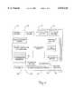
- FIG. 1is a block diagram of a prior art personal computer employing an ISA bus, a PCI bus, and also a system bus.
- FIG. 2is a block diagram of the components of the core logic or chipset typically used in modern personal computers.
- FIG. 3is a block diagram of a personal computer where the ROM BIOS is attached to the system bus.
- FIG. 4is a more detailed block diagram of the interface between the ROM BIOS and the system bus in FIG. 3.
- FIG. 1is a block diagram of a prior art x86 personal computer 100, including a processor 112 and a chip set or core logic 114.
- the processor 112is connected to the system memory bus 118 by the chip set 114.
- the memory bus 118has a 32-bit address bus and also a 64-bit data bus.
- the computer 100also includes two additional busses, the Peripheral Component Interconnect (PCI) bus 120 and the Industry Standard Architecture (ISA) bus 122.
- PCIPeripheral Component Interconnect
- ISAIndustry Standard Architecture
- the PCI bus 120is a typically a 32-bit bus on which data and address signals are multiplexed. (The PCI bus 120 can be extended to 64 bits.)
- the PCI busis essentially a mezzanine bus that is connected to the system bus 118 through bridge logic 124.
- a PCI peripheral device 130which might be a video adapter or hard disk drive controller, is shown attached to the PCI bus in FIG. 1.
- the PCI bus 120is also connected to the ISA bus 122 in FIG. 1 through the ISA bridge 128.
- the ISA bus 122 shown in FIG. 1is the standard bus found in almost every IBM-compatible computer manufactured in the last fifteen years.
- the ISA bus 122includes a 20-bit address bus and a 16-bit data bus. Attached to the ISA bus 122 is an ISA peripheral device 132.
- Also connected to the ISA bus 122is the ROM BIOS 110. As is well known in the art, stored in the ROM BIOS are various support routines and data used at power-up, as well as I/O support routines for accessing the keyboard, the graphics adapter, and other devices.
- the ROM BIOS 110 in FIG. 1is implemented by a non-volatile, electrically block-erasable, programmable read-only memory device (e.g., a FLASH memory device). Such a device can be periodically erased and rewritten, thereby permitting re-programming of the BIOS region.
- ROM BIOS accesscan be very slow, particularly where a FLASH ROM is used. For this reason, the BIOS routines are usually switched out of the ROM device it initially occupies, and into faster "shadow" memory (e.g., DRAM) at the same addresses.
- the contents of the ROM BIOSmay be compressed, so it may be necessary to decompress it as it is moved into shadow RAM.
- BIOSThe movement of the BIOS into shadow RAM typically takes place just after system reset, and once complete, the ROM device is generally not accessed again until a system reset. Once BIOS is shadowed, all accesses to the BIOS are directed to shadow RAM, rather than the ROM device. Because this shadow RAM is significantly faster than the ROM device, access to the BIOS routines is much faster.
- BIOS routineswhich may be stored in the device 110 in FIG. 1 are generally required to be accessible only to the CPU and, in a 32-bit address space, are addressed at the top 256 Mb of memory space (since that is where the CPU starts after a reset) and in the top 128 Kb of the low 1 megabyte of memory space.
- a memory cycleis indicated by a MEMCYCLE signal, and where a ROMEN signal indicates whether access to the ROM BIOS device is enabled
- an access to a BIOS routinecan be detected when the following expression evaluates to a logical one:
- the signal ROMENwould be controlled by bits in the configuration registers 190 for the chipset 114. (See FIG. 2.) After system reset, read access to the ROM device is permitted and writes are permitted in the same addresses in the shadow RAM, which allows the move/decompress operation to take place. Once shadowing has occurred, the ROM would no longer be accessible. However, read operations to the corresponding shadow RAM address space would be permitted, but write operations to this region of RAM would be prohibited. (Note that during programming of the (FLASH) ROM BIOS device, erasure or write operations can be performed on the ROM device.)
- the shadowing procedure known in the art and described aboveavoids subsequent accesses to the ROM device after its contents are shadowed to faster RAM, but this shadowing procedure does not eliminate the need for the ROM device.
- the ROM devicestill will typically be required so that the BIOS routines can be stored in a non-volatile manner. These BIOS routines must also be accessible by the CPU, which has traditionally required an ISA bus. Yet the ROM BIOS may be one of the only devices on the ISA bus, so the ROM BIOS and the other support it requires (e.g., the ISA bus and associated logic) can require a significant amount of hardware, and can account for a non-trivial percentage of the cost of a computer system.
- the present inventionmoves the ROM BIOS to another bus within the computer system, thereby eliminating the ROM BIOS' dependence on the ISA bus. In some computer systems, this will allow the ISA bus to be eliminated from the system entirely, saving significant costs.
- FIG. 2is a block diagram of the chip set or core logic 114 used in some embodiments of the present invention.
- the chip set 114includes logic for address decoding 181, logic for cycle type decoding 182, data buffers 183, and a host state machine 184. Numerous other logic modules are also shown in FIG. 2, including modules for PCI arbitration 185, PCI address decoding 186, PCI Address/Data Mux/Demux 187, PCI Buffers 188, and a PCI State Machine 189.
- the chip set 114 or core logicis often constructed of multiple discrete parts, each of which includes one or more of the modules shown in FIG. 2. However, the same functionality could be obtained in another embodiment by integrating one or more of these separate modules into a single part.
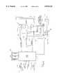
- FIG. 3shows a block diagram of a personal computer based on an x86-based processor.
- the ROM BIOS 110is attached to the system memory address and data bus 118, rather than to the ISA bus as shown in FIG. 1.
- the eight-bit data path from the ROM BIOS 110is attached to the memory data bus 183 182 through a buffer or latch 220, which buffers the data between the ROM BIOS and the system memory bus 118.
- eighteen address lines 151are used for the ROM BIOS, and the ROM BIOS address ports are connected to the memory address bus over lines 182, and a portion of the memory data bus 183.
- the additional lines 152may be used for control signalling.
- FIG. 4is a more detailed and modified block diagram of FIG. 3, where the ROM BIOS 110 is implemented as a FLASH ROM device that contains the BIOS routines and associated initialization code.
- the core logic 170controls access to the main memory 174, and interfaces with the video controller 117 through the accelerated graphics port bus 119.
- the core logic 170also administers the transfer of data from the ROM BIOS 110.
- the ROM BIOS addressesare passed from the memory bus 118 to the ROM BIOS 110 over address lines 151. Unlike the address lines 151 in FIG. 3, the address lines that extend to the BIOS device 110 are taken from both the system address bus 182, and the system data bus 183. In the embodiment shown in FIG.
- the memory 174uses a multiplexed addressing scheme, which allows the address bus to be only fourteen bits wide (yet addressable with a twenty-eight bit address). For the remaining four bits that the BIOS device may require for its address, a portion of the system data bus 183 is used, as is shown in FIG. 4. Data is passed between the ROM BIOS 110 and the core logic 170 over bus 153, through buffer 220, and over the system data bus 183. Signals 152 are used to control the transfer of data to or from the FLASH memory device 110.
- a ROM BIOS accessis initiated by decoding the address on the system address bus 182, and allowing any other operations involving the memory bus to be completed.
- the core logic 170then accesses the ROM BIOS 110 by placing an address on the memory address bus 182, and a portion of the memory data bus 183.
- the core logic 170places the ROM address on these busses 182 and 183 by placing fourteen bits on the address bus 182, and the remaining four bits on the data bus 183 (e.g., on lines D8 to D11). It is thereby communicated to the ROM BIOS 110 over lines 151.
- the ROM BIOS 110After an appropriate period of time (e.g., the ROM access time), the ROM BIOS 110 responds by placing the addressed data (typically an 8 bit quantity) on bus 153.
- the datamay be gated through a buffer 220, and onto a different portion of the system data bus (e.g., lines D0 to D7).
- the buffermay be omitted when signalling levels are compatible and the bus is lightly loaded.
- the address and datapreferably occupy two different portions of the system data bus 183.
- the control signals shown in FIG. 4include output enable (OE), write enable (WE), and chip enable (CE) signals. These control signals (as well as any others that are not shown) are preferably passed to the ROM BIOS on other lines on the memory control bus or on the system data bus as shown. It may be possible to multiplex the BIOS address and/or data on a smaller number of lines on the memory bus, but since there are typically enough lines available on the bus, it is preferred that different lines be used for address, data, and control signals as described.
- OEoutput enable
- WEwrite enable
- CEchip enable
- the width of the data from the ROMis normally 8 bits, whereas the CPU data path is normally much larger (e.g., 64 bits).
- the core logic 170sequences the lower address bits presented to the ROM BIOS 110 so that more than one eight-bit quantity can be read from the ROM BIOS. For example, for a 64-bit CPU data path, the core logic 170 can sequence the lower three bits of the ROM address eight times so that eight bytes of data are read from the ROM BIOS 110 in succession, thereby completing a full 64-bit data word.
- the core logic 170is capable of constructing a larger data quantity (e.g., 32-bits or 64 bits) by aggregating multiple eight bit data units from the ROM BIOS. It may also be more efficient in some embodiments for the core logic to construct a full line of data (e.g., four or two 64-bit quantities). Other performance-enhancing techniques, such as the shadowing operation described above, could also be used with the present invention, and should be understood to be within the scope of the present invention.
- FIGS. 3 and 4By configuring a computer system as shown in FIGS. 3 and 4, it is possible to attach the ROM BIOS to the memory bus 118, thereby potentially eliminating the need for the ISA bus. The present invention will therefore reduce system complexity and manufacturing costs, and may also enhance system performance. Although a discrete implementation is shown in FIGS. 3 and 4 using multiple parts, it should be understood that the present invention encompasses implementations and embodiments where some or all of the equivalent logic is integrated into the core logic 170 or into the ROM BIOS or FLASH memory device 110.
Landscapes
- Engineering & Computer Science (AREA)
- Theoretical Computer Science (AREA)
- Physics & Mathematics (AREA)
- General Engineering & Computer Science (AREA)
- General Physics & Mathematics (AREA)
- Stored Programmes (AREA)
Abstract
Description
Claims (16)
Priority Applications (1)
| Application Number | Priority Date | Filing Date | Title |
|---|---|---|---|
| US08/941,663US6076118A (en) | 1997-09-30 | 1997-09-30 | Attachment or integration of a BIOS device into a computer system using the system memory address and data bus |
Applications Claiming Priority (1)
| Application Number | Priority Date | Filing Date | Title |
|---|---|---|---|
| US08/941,663US6076118A (en) | 1997-09-30 | 1997-09-30 | Attachment or integration of a BIOS device into a computer system using the system memory address and data bus |
Publications (1)
| Publication Number | Publication Date |
|---|---|
| US6076118Atrue US6076118A (en) | 2000-06-13 |
Family
ID=25476857
Family Applications (1)
| Application Number | Title | Priority Date | Filing Date |
|---|---|---|---|
| US08/941,663Expired - LifetimeUS6076118A (en) | 1997-09-30 | 1997-09-30 | Attachment or integration of a BIOS device into a computer system using the system memory address and data bus |
Country Status (1)
| Country | Link |
|---|---|
| US (1) | US6076118A (en) |
Cited By (4)
| Publication number | Priority date | Publication date | Assignee | Title |
|---|---|---|---|---|
| US6629192B1 (en)* | 1999-12-30 | 2003-09-30 | Intel Corporation | Method and apparatus for use of a non-volatile storage management system for PC/AT compatible system firmware |
| WO2004031960A1 (en)* | 2002-10-01 | 2004-04-15 | Texas Instruments Incorporated | Flash emulator |
| US6732261B2 (en) | 1999-12-30 | 2004-05-04 | Intel Corporation | Method and apparatus for implementing a register scan process |
| US7302698B1 (en)* | 1999-09-17 | 2007-11-27 | Hewlett-Packard Development Company, L.P. | Operation of trusted state in computing platform |
Citations (27)
| Publication number | Priority date | Publication date | Assignee | Title |
|---|---|---|---|---|
| US4933845A (en)* | 1987-09-04 | 1990-06-12 | Digital Equipment Corporation | Reconfigurable bus |
| US5193170A (en)* | 1990-10-26 | 1993-03-09 | International Business Machines Corporation | Methods and apparatus for maintaining cache integrity whenever a cpu write to rom operation is performed with rom mapped to ram |
| US5414820A (en)* | 1991-08-23 | 1995-05-09 | Nexgen, Inc. | Crossing transfers for maximizing the effective bandwidth in a dual-bus architecture |
| US5450458A (en)* | 1994-08-05 | 1995-09-12 | International Business Machines Corporation | Method and apparatus for phase-aligned multiple frequency synthesizer with synchronization window decoder |
| US5457785A (en)* | 1993-02-10 | 1995-10-10 | Elonex Technologies, Inc. | CPU-independent and device-driver transparent system for translating a computer's internal bus signals onto an intermediate bus and further translating onto an expansion bus |
| US5522076A (en)* | 1993-05-13 | 1996-05-28 | Kabushiki Kaisha Toshiba | Computer system having BIOS (basic input/output system)-ROM (Read Only Memory) writing function |
| US5559966A (en)* | 1992-11-06 | 1996-09-24 | Intel Corporation | Method and apparatus for interfacing a bus that operates at a plurality of operating potentials |
| US5584040A (en)* | 1992-10-20 | 1996-12-10 | Cirrus Logic, Inc. | High performance peripheral interface with read-ahead capability |
| US5594874A (en)* | 1993-09-30 | 1997-01-14 | Cirrus Logic, Inc. | Automatic bus setting, sensing and switching interface unit |
| US5596735A (en)* | 1996-02-23 | 1997-01-21 | Cyrix Corporation | Circuit and method for addressing segment descriptor tables |
| US5596740A (en)* | 1995-01-26 | 1997-01-21 | Cyrix Corporation | Interleaved memory conflict resolution with accesses of variable bank widths and partial return of non-conflicting banks |
| US5623691A (en)* | 1994-11-14 | 1997-04-22 | Compaq Computer Corporation | PCI bus hard disk activity LED circuit |
| US5657285A (en)* | 1995-07-14 | 1997-08-12 | Cirrus Logic, Inc. | Pipelined address memories, and systems and methods using the same |
| US5680620A (en)* | 1995-06-30 | 1997-10-21 | Dell Usa, L.P. | System and method for detecting access to a peripheral device using a debug register |
| US5721882A (en)* | 1994-08-05 | 1998-02-24 | Intel Corporation | Method and apparatus for interfacing memory devices operating at different speeds to a computer system bus |
| US5740387A (en)* | 1995-11-20 | 1998-04-14 | Advanced Micro Devices, Inc. | Computer system having an expansion bus which includes normal and real time modes |
| US5740381A (en)* | 1995-12-22 | 1998-04-14 | United Microelectronics Corporation | Expandable arbitration architecture for sharing system memory in a computer system |
| US5778431A (en)* | 1995-12-19 | 1998-07-07 | Advanced Micro Devices, Inc. | System and apparatus for partially flushing cache memory |
| US5787306A (en)* | 1994-05-18 | 1998-07-28 | National Semiconductor Corporation | Automatic assignment of I/O addresses in a computer system |
| US5794054A (en)* | 1996-07-19 | 1998-08-11 | Compaq Computer Corporation | Flash ROM sharing between a processor and a controller |
| US5802324A (en)* | 1996-12-23 | 1998-09-01 | Compaq Computer Corporation | Computer system with PCI repeater between primary bus and second bus |
| US5809262A (en)* | 1995-05-17 | 1998-09-15 | Dell U.S.A., L.P. | Commonly housed multiple processor type computing system and method of manufacturing the same |
| US5822768A (en)* | 1996-01-11 | 1998-10-13 | Opti Inc. | Dual ported memory for a unified memory architecture |
| US5826015A (en)* | 1997-02-20 | 1998-10-20 | Digital Equipment Corporation | Method and apparatus for secure remote programming of firmware and configurations of a computer over a network |
| US5835760A (en)* | 1995-10-13 | 1998-11-10 | Texas Instruments Incorporated | Method and arrangement for providing BIOS to a host computer |
| US5857086A (en)* | 1997-05-13 | 1999-01-05 | Compaq Computer Corp. | Apparatus method and system for peripheral component interconnect bus using accelerated graphics port logic circuits |
| US5859989A (en)* | 1997-05-13 | 1999-01-12 | Compaq Computer Corp. | Apparatus method and system for 64 bit peripheral component interconnect bus using accelerated graphics port logic circuits |
- 1997
- 1997-09-30USUS08/941,663patent/US6076118A/ennot_activeExpired - Lifetime
Patent Citations (27)
| Publication number | Priority date | Publication date | Assignee | Title |
|---|---|---|---|---|
| US4933845A (en)* | 1987-09-04 | 1990-06-12 | Digital Equipment Corporation | Reconfigurable bus |
| US5193170A (en)* | 1990-10-26 | 1993-03-09 | International Business Machines Corporation | Methods and apparatus for maintaining cache integrity whenever a cpu write to rom operation is performed with rom mapped to ram |
| US5414820A (en)* | 1991-08-23 | 1995-05-09 | Nexgen, Inc. | Crossing transfers for maximizing the effective bandwidth in a dual-bus architecture |
| US5584040A (en)* | 1992-10-20 | 1996-12-10 | Cirrus Logic, Inc. | High performance peripheral interface with read-ahead capability |
| US5559966A (en)* | 1992-11-06 | 1996-09-24 | Intel Corporation | Method and apparatus for interfacing a bus that operates at a plurality of operating potentials |
| US5457785A (en)* | 1993-02-10 | 1995-10-10 | Elonex Technologies, Inc. | CPU-independent and device-driver transparent system for translating a computer's internal bus signals onto an intermediate bus and further translating onto an expansion bus |
| US5522076A (en)* | 1993-05-13 | 1996-05-28 | Kabushiki Kaisha Toshiba | Computer system having BIOS (basic input/output system)-ROM (Read Only Memory) writing function |
| US5594874A (en)* | 1993-09-30 | 1997-01-14 | Cirrus Logic, Inc. | Automatic bus setting, sensing and switching interface unit |
| US5787306A (en)* | 1994-05-18 | 1998-07-28 | National Semiconductor Corporation | Automatic assignment of I/O addresses in a computer system |
| US5721882A (en)* | 1994-08-05 | 1998-02-24 | Intel Corporation | Method and apparatus for interfacing memory devices operating at different speeds to a computer system bus |
| US5450458A (en)* | 1994-08-05 | 1995-09-12 | International Business Machines Corporation | Method and apparatus for phase-aligned multiple frequency synthesizer with synchronization window decoder |
| US5623691A (en)* | 1994-11-14 | 1997-04-22 | Compaq Computer Corporation | PCI bus hard disk activity LED circuit |
| US5596740A (en)* | 1995-01-26 | 1997-01-21 | Cyrix Corporation | Interleaved memory conflict resolution with accesses of variable bank widths and partial return of non-conflicting banks |
| US5809262A (en)* | 1995-05-17 | 1998-09-15 | Dell U.S.A., L.P. | Commonly housed multiple processor type computing system and method of manufacturing the same |
| US5680620A (en)* | 1995-06-30 | 1997-10-21 | Dell Usa, L.P. | System and method for detecting access to a peripheral device using a debug register |
| US5657285A (en)* | 1995-07-14 | 1997-08-12 | Cirrus Logic, Inc. | Pipelined address memories, and systems and methods using the same |
| US5835760A (en)* | 1995-10-13 | 1998-11-10 | Texas Instruments Incorporated | Method and arrangement for providing BIOS to a host computer |
| US5740387A (en)* | 1995-11-20 | 1998-04-14 | Advanced Micro Devices, Inc. | Computer system having an expansion bus which includes normal and real time modes |
| US5778431A (en)* | 1995-12-19 | 1998-07-07 | Advanced Micro Devices, Inc. | System and apparatus for partially flushing cache memory |
| US5740381A (en)* | 1995-12-22 | 1998-04-14 | United Microelectronics Corporation | Expandable arbitration architecture for sharing system memory in a computer system |
| US5822768A (en)* | 1996-01-11 | 1998-10-13 | Opti Inc. | Dual ported memory for a unified memory architecture |
| US5596735A (en)* | 1996-02-23 | 1997-01-21 | Cyrix Corporation | Circuit and method for addressing segment descriptor tables |
| US5794054A (en)* | 1996-07-19 | 1998-08-11 | Compaq Computer Corporation | Flash ROM sharing between a processor and a controller |
| US5802324A (en)* | 1996-12-23 | 1998-09-01 | Compaq Computer Corporation | Computer system with PCI repeater between primary bus and second bus |
| US5826015A (en)* | 1997-02-20 | 1998-10-20 | Digital Equipment Corporation | Method and apparatus for secure remote programming of firmware and configurations of a computer over a network |
| US5857086A (en)* | 1997-05-13 | 1999-01-05 | Compaq Computer Corp. | Apparatus method and system for peripheral component interconnect bus using accelerated graphics port logic circuits |
| US5859989A (en)* | 1997-05-13 | 1999-01-12 | Compaq Computer Corp. | Apparatus method and system for 64 bit peripheral component interconnect bus using accelerated graphics port logic circuits |
Cited By (4)
| Publication number | Priority date | Publication date | Assignee | Title |
|---|---|---|---|---|
| US7302698B1 (en)* | 1999-09-17 | 2007-11-27 | Hewlett-Packard Development Company, L.P. | Operation of trusted state in computing platform |
| US6629192B1 (en)* | 1999-12-30 | 2003-09-30 | Intel Corporation | Method and apparatus for use of a non-volatile storage management system for PC/AT compatible system firmware |
| US6732261B2 (en) | 1999-12-30 | 2004-05-04 | Intel Corporation | Method and apparatus for implementing a register scan process |
| WO2004031960A1 (en)* | 2002-10-01 | 2004-04-15 | Texas Instruments Incorporated | Flash emulator |
Similar Documents
| Publication | Publication Date | Title |
|---|---|---|
| EP0631241B1 (en) | Initializing multiple bus networks | |
| US5826093A (en) | Dual function disk drive integrated circuit for master mode and slave mode operations | |
| US6308248B1 (en) | Method and system for allocating memory space using mapping controller, page table and frame numbers | |
| US5937423A (en) | Register interface for flash EEPROM memory arrays | |
| US5642489A (en) | Bridge between two buses of a computer system with a direct memory access controller with accessible registers to support power management | |
| US6279069B1 (en) | Interface for flash EEPROM memory arrays | |
| US7890690B2 (en) | System and method for dual-ported flash memory | |
| US5724529A (en) | Computer system with multiple PC card controllers and a method of controlling I/O transfers in the system | |
| JP2633458B2 (en) | DMA channel device and DMA channel conversion device | |
| US7185135B1 (en) | USB to PCI bridge | |
| JP2519401B2 (en) | Control method and device for PCI expansion card | |
| US5542053A (en) | Bridge interface between two buses of a computer system with a direct memory access controller programmed by a scatter/gather programmer | |
| EP0657818A1 (en) | Non-volatile memory chip enable signal encoding method and system | |
| WO1998035295A1 (en) | Method and apparatus for enabling intelligent i/o subsystems using pci i/o devices | |
| US5630099A (en) | Non-volatile memory array controller capable of controlling memory banks having variable bit widths | |
| US5603055A (en) | Single shared ROM for storing keyboard microcontroller code portion and CPU code portion and disabling access to a portion while accessing to the other | |
| US5649162A (en) | Local bus interface | |
| KR100297202B1 (en) | Improved interface for flash eeprom memory arrays | |
| US6003103A (en) | Method for attachment or integration of a bios device into a computer system using a local bus | |
| US7058779B1 (en) | Computer system initialization via boot code stored in a non-volatile memory having an interface compatible with synchronous dynamic random access memory | |
| US6742058B2 (en) | Memory controller having a multiplexer selecting either second set of input signals or converted signals from first set of input signals by a bus mode input | |
| US5448521A (en) | Connecting a short word length non-volatile memory to a long word length address/data multiplexed bus | |
| US7249253B2 (en) | Booting from a re-programmable memory on an unconfigured bus | |
| EP3270293B1 (en) | Two stage command buffers to overlap iommu map and second tier memory reads | |
| US5961643A (en) | Method for attachment or integration of a BIOS device into a computer system using the system memory address and data bus |
Legal Events
| Date | Code | Title | Description |
|---|---|---|---|
| AS | Assignment | Owner name:MICRON ELECTRONICS, INC., IDAHO Free format text:ASSIGNMENT OF ASSIGNORS INTEREST;ASSIGNOR:KLEIN, DEAN A.;REEL/FRAME:009021/0841 Effective date:19971107 | |
| STCF | Information on status: patent grant | Free format text:PATENTED CASE | |
| AS | Assignment | Owner name:MEI CALIFORNIA, INC., CALIFORNIA Free format text:ASSIGNMENT OF ASSIGNORS INTEREST;ASSIGNOR:MICRON ELECTRONICS, INC.;REEL/FRAME:011658/0956 Effective date:20010322 | |
| FPAY | Fee payment | Year of fee payment:4 | |
| FPAY | Fee payment | Year of fee payment:8 | |
| FPAY | Fee payment | Year of fee payment:12 | |
| AS | Assignment | Owner name:U.S. BANK NATIONAL ASSOCIATION, AS COLLATERAL AGENT, CALIFORNIA Free format text:SECURITY INTEREST;ASSIGNOR:MICRON TECHNOLOGY, INC.;REEL/FRAME:038669/0001 Effective date:20160426 Owner name:U.S. BANK NATIONAL ASSOCIATION, AS COLLATERAL AGEN Free format text:SECURITY INTEREST;ASSIGNOR:MICRON TECHNOLOGY, INC.;REEL/FRAME:038669/0001 Effective date:20160426 | |
| AS | Assignment | Owner name:MORGAN STANLEY SENIOR FUNDING, INC., AS COLLATERAL AGENT, MARYLAND Free format text:PATENT SECURITY AGREEMENT;ASSIGNOR:MICRON TECHNOLOGY, INC.;REEL/FRAME:038954/0001 Effective date:20160426 Owner name:MORGAN STANLEY SENIOR FUNDING, INC., AS COLLATERAL Free format text:PATENT SECURITY AGREEMENT;ASSIGNOR:MICRON TECHNOLOGY, INC.;REEL/FRAME:038954/0001 Effective date:20160426 | |
| AS | Assignment | Owner name:U.S. BANK NATIONAL ASSOCIATION, AS COLLATERAL AGENT, CALIFORNIA Free format text:CORRECTIVE ASSIGNMENT TO CORRECT THE REPLACE ERRONEOUSLY FILED PATENT #7358718 WITH THE CORRECT PATENT #7358178 PREVIOUSLY RECORDED ON REEL 038669 FRAME 0001. ASSIGNOR(S) HEREBY CONFIRMS THE SECURITY INTEREST;ASSIGNOR:MICRON TECHNOLOGY, INC.;REEL/FRAME:043079/0001 Effective date:20160426 Owner name:U.S. BANK NATIONAL ASSOCIATION, AS COLLATERAL AGEN Free format text:CORRECTIVE ASSIGNMENT TO CORRECT THE REPLACE ERRONEOUSLY FILED PATENT #7358718 WITH THE CORRECT PATENT #7358178 PREVIOUSLY RECORDED ON REEL 038669 FRAME 0001. ASSIGNOR(S) HEREBY CONFIRMS THE SECURITY INTEREST;ASSIGNOR:MICRON TECHNOLOGY, INC.;REEL/FRAME:043079/0001 Effective date:20160426 | |
| AS | Assignment | Owner name:MICRON TECHNOLOGY, INC., IDAHO Free format text:RELEASE BY SECURED PARTY;ASSIGNOR:U.S. BANK NATIONAL ASSOCIATION, AS COLLATERAL AGENT;REEL/FRAME:047243/0001 Effective date:20180629 | |
| AS | Assignment | Owner name:MICRON TECHNOLOGY, INC., IDAHO Free format text:RELEASE BY SECURED PARTY;ASSIGNOR:MORGAN STANLEY SENIOR FUNDING, INC., AS COLLATERAL AGENT;REEL/FRAME:050937/0001 Effective date:20190731 |