US6074909A - Apparatus and method for forming controlled deep trench top isolation layers - Google Patents
Apparatus and method for forming controlled deep trench top isolation layersDownload PDFInfo
- Publication number
- US6074909A US6074909AUS09/127,262US12726298AUS6074909AUS 6074909 AUS6074909 AUS 6074909AUS 12726298 AUS12726298 AUS 12726298AUS 6074909 AUS6074909 AUS 6074909A
- Authority
- US
- United States
- Prior art keywords
- trench
- isolation layer
- isolation
- layer
- recited
- Prior art date
- Legal status (The legal status is an assumption and is not a legal conclusion. Google has not performed a legal analysis and makes no representation as to the accuracy of the status listed.)
- Expired - Lifetime
Links
- 238000002955isolationMethods0.000titleclaimsabstractdescription150
- 238000000034methodMethods0.000titleclaimsabstractdescription56
- 238000003860storageMethods0.000claimsabstractdescription46
- 239000000758substrateSubstances0.000claimsabstractdescription45
- 239000004065semiconductorSubstances0.000claimsabstractdescription40
- 238000000151depositionMethods0.000claimsabstractdescription27
- 230000000873masking effectEffects0.000claimsabstractdescription27
- 230000015654memoryEffects0.000claimsabstractdescription16
- 239000004020conductorSubstances0.000claimsdescription33
- 238000005530etchingMethods0.000claimsdescription20
- 229910021420polycrystalline siliconInorganic materials0.000claimsdescription16
- 229920005591polysiliconPolymers0.000claimsdescription16
- 239000000463materialSubstances0.000claimsdescription15
- 239000003989dielectric materialSubstances0.000claimsdescription14
- 150000004767nitridesChemical class0.000claimsdescription12
- 230000008569processEffects0.000claimsdescription12
- 238000005229chemical vapour depositionMethods0.000claimsdescription6
- 238000004891communicationMethods0.000claimsdescription6
- 239000000126substanceSubstances0.000claimsdescription5
- 238000000623plasma-assisted chemical vapour depositionMethods0.000claimsdescription4
- 230000008878couplingEffects0.000claimsdescription3
- 238000010168coupling processMethods0.000claimsdescription3
- 238000005859coupling reactionMethods0.000claimsdescription3
- 230000004913activationEffects0.000claimsdescription2
- 230000008021depositionEffects0.000description9
- PEDCQBHIVMGVHV-UHFFFAOYSA-NGlycerineChemical compoundOCC(O)COPEDCQBHIVMGVHV-UHFFFAOYSA-N0.000description6
- 239000000945fillerSubstances0.000description6
- 238000001039wet etchingMethods0.000description6
- VYPSYNLAJGMNEJ-UHFFFAOYSA-NSilicium dioxideChemical compoundO=[Si]=OVYPSYNLAJGMNEJ-UHFFFAOYSA-N0.000description5
- 238000005137deposition processMethods0.000description5
- 238000001312dry etchingMethods0.000description5
- 230000015572biosynthetic processEffects0.000description4
- 230000006870functionEffects0.000description4
- 238000005468ion implantationMethods0.000description4
- 229910052581Si3N4Inorganic materials0.000description3
- HQVNEWCFYHHQES-UHFFFAOYSA-Nsilicon nitrideChemical compoundN12[Si]34N5[Si]62N3[Si]51N64HQVNEWCFYHHQES-UHFFFAOYSA-N0.000description3
- 239000005380borophosphosilicate glassSubstances0.000description2
- 238000013461designMethods0.000description2
- 238000001020plasma etchingMethods0.000description2
- 229910021332silicideInorganic materials0.000description2
- FVBUAEGBCNSCDD-UHFFFAOYSA-Nsilicide(4-)Chemical compound[Si-4]FVBUAEGBCNSCDD-UHFFFAOYSA-N0.000description2
- 235000012239silicon dioxideNutrition0.000description2
- 239000000377silicon dioxideSubstances0.000description2
- WQJQOUPTWCFRMM-UHFFFAOYSA-Ntungsten disilicideChemical compound[Si]#[W]#[Si]WQJQOUPTWCFRMM-UHFFFAOYSA-N0.000description2
- -1tungsten silicideChemical compound0.000description2
- 229910021342tungsten silicideInorganic materials0.000description2
- JBRZTFJDHDCESZ-UHFFFAOYSA-NAsGaChemical compound[As]#[Ga]JBRZTFJDHDCESZ-UHFFFAOYSA-N0.000description1
- 229910001218Gallium arsenideInorganic materials0.000description1
- XUIMIQQOPSSXEZ-UHFFFAOYSA-NSiliconChemical compound[Si]XUIMIQQOPSSXEZ-UHFFFAOYSA-N0.000description1
- 230000009471actionEffects0.000description1
- 239000011248coating agentSubstances0.000description1
- 238000000576coating methodMethods0.000description1
- 239000011231conductive fillerSubstances0.000description1
- 230000003116impacting effectEffects0.000description1
- 150000002500ionsChemical class0.000description1
- 238000004519manufacturing processMethods0.000description1
- 238000012986modificationMethods0.000description1
- 230000004048modificationEffects0.000description1
- 230000003647oxidationEffects0.000description1
- 238000007254oxidation reactionMethods0.000description1
- 238000012545processingMethods0.000description1
- 229910052710siliconInorganic materials0.000description1
- 239000010703siliconSubstances0.000description1
- 229910052814silicon oxideInorganic materials0.000description1
Images


Classifications
- H—ELECTRICITY
- H10—SEMICONDUCTOR DEVICES; ELECTRIC SOLID-STATE DEVICES NOT OTHERWISE PROVIDED FOR
- H10B—ELECTRONIC MEMORY DEVICES
- H10B12/00—Dynamic random access memory [DRAM] devices
- H10B12/01—Manufacture or treatment
- H10B12/02—Manufacture or treatment for one transistor one-capacitor [1T-1C] memory cells
- H10B12/03—Making the capacitor or connections thereto
- H10B12/038—Making the capacitor or connections thereto the capacitor being in a trench in the substrate
- H—ELECTRICITY
- H01—ELECTRIC ELEMENTS
- H01L—SEMICONDUCTOR DEVICES NOT COVERED BY CLASS H10
- H01L21/00—Processes or apparatus adapted for the manufacture or treatment of semiconductor or solid state devices or of parts thereof
- H01L21/02—Manufacture or treatment of semiconductor devices or of parts thereof
- H01L21/04—Manufacture or treatment of semiconductor devices or of parts thereof the devices having potential barriers, e.g. a PN junction, depletion layer or carrier concentration layer
- H01L21/18—Manufacture or treatment of semiconductor devices or of parts thereof the devices having potential barriers, e.g. a PN junction, depletion layer or carrier concentration layer the devices having semiconductor bodies comprising elements of Group IV of the Periodic Table or AIIIBV compounds with or without impurities, e.g. doping materials
- H01L21/28—Manufacture of electrodes on semiconductor bodies using processes or apparatus not provided for in groups H01L21/20 - H01L21/268
- H01L21/283—Deposition of conductive or insulating materials for electrodes conducting electric current
- H—ELECTRICITY
- H10—SEMICONDUCTOR DEVICES; ELECTRIC SOLID-STATE DEVICES NOT OTHERWISE PROVIDED FOR
- H10B—ELECTRONIC MEMORY DEVICES
- H10B12/00—Dynamic random access memory [DRAM] devices
- H10B12/01—Manufacture or treatment
- H10B12/02—Manufacture or treatment for one transistor one-capacitor [1T-1C] memory cells
- H10B12/05—Making the transistor
- H10B12/053—Making the transistor the transistor being at least partially in a trench in the substrate
- H—ELECTRICITY
- H10—SEMICONDUCTOR DEVICES; ELECTRIC SOLID-STATE DEVICES NOT OTHERWISE PROVIDED FOR
- H10B—ELECTRONIC MEMORY DEVICES
- H10B12/00—Dynamic random access memory [DRAM] devices
- H10B12/30—DRAM devices comprising one-transistor - one-capacitor [1T-1C] memory cells
- H10B12/48—Data lines or contacts therefor
- H10B12/488—Word lines
Definitions
- This disclosurerelate s to semiconductor devices and more particularly, to an apparatus and method for forming deep trench isolation layers for semiconductor memories.
- DRAMdynamic random access memories
- Semiconductor memoriessuch as dynamic random access memories (DRAM) typically include memory cells. These memory cells include storage nodes. Generally these storage nodes are formed with in deep trenches etched into substrates of the semiconductor memory chip. The storage nodes are accessed using an access transistor which allows charge to be stored in the storage node or retrieves charge from the storage depending on whether the desired action is a read or write function. It is often necessary to ensure that the storage node is sufficiently electrically isolated from a gate conductor.
- the storage nodestypically include polysilicon material that partially fills the deep trench. During fabrication the polysilicon leaves a recess remaining at the top of the trench. An oxide (silicon dioxide) is deposited over the surface of the semiconductor device. During the oxide deposition, oxide is formed over the polysilicon in the trench. Other portions of the deposited oxide are removed by planarizing the surface of the semiconductor device and by recessing the oxide to leave a 30-50 nm oxide layer at the bottom of the recess. This oxide layer is referred to as a trench top oxide or isolation.
- the oxide recessingis difficult to control. This difficulty introduces a lot of variability in the remaining oxide layer thickness.
- the trench top oxide thicknessis an important parameter and must be maintained in order for the semiconductor memory to work properly. As described above, the trench top oxide electrically isolates the storage node from the gate conductor of the semiconductor device.
- a method for controlling isolation layer thickness in deep trenches for semiconductor memories in accordance with the present inventionincludes the steps of providing a deep trench having a storage node formed therein, the storage node having a buried strap, depositing an isolation layer on the buried strap for providing electrical isolation for the storage node, forming a masking layer on the isolation layer to mask a portion of the isolation layer in contact with the buried strap and removing the isolation layer except the portion masked by the mask layer such that control of a thickness of the isolation layer is improved.
- the step of depositing the isolation layermay include depositing the isolation layer by chemical vapor deposition or by plasma enhanced chemical vapor deposition.
- the isolation layermay include an oxide, a nitride or a combination of both.
- the thickness of the isolation layeris preferably between about 20 nm to about 50 nm.
- the step of forming the masking layermay include the step of depositing a material which is selectively etchable relative to the isolation layer.
- the materialmay include polysilicon.
- a method for fabricating a memory cell having trench isolationincludes the steps of providing a deep trench having a storage node formed therein, the storage node having a buried strap, depositing an isolation layer on the buried strap for providing electrical isolation for the storage node, forming a masking layer on the isolation layer to mask a portion of the isolation layer in contact with the buried strap, selectively etching the isolation layer relative to the masking layer to leave the portion masked by the masking layer, opening up an isolation trench in communication with the deep trench by removing at least a portion of the substrate adjacent to the deep trench, filling the isolation trench with a dielectric material to provide trench isolation.
- the step of forming an access device for accessing the storage node disposed within the trench below the isolation layeris preferably included.
- the step of forming an access devicemay include forming a transistor having a channel formed in the substrate for electrically coupling the buried strap to a bitline.
- the step of recessing the portion of the substrate adjacent to the deep trench such that the transistor is formed a greater distance away from the deep trenchis preferably included.
- the step of forming a transistor gate adjacent to the trench isolation and adjacent to the isolation layer in a top portion of the deep trenchmay also be included.
- the isolation layermay be deposited by chemical vapor deposition.
- the isolation layermay include an oxide a nitride or a combination of both.
- the thickness of the isolation layeris preferably between about 20 nm to about 50 nm.
- the masking layermay include polysilicon.
- the trench isolationmay include shallow trench isolation or raised shallow trench isolation.
- a method for fabricating a vertical transistorincludes the steps of providing a substrate having trenches formed therein, each trench having a storage node formed therein, the storage node having a buried strap, forming an isolation layer on the buried strap, laterally etching the substrate to recess a step into the substrate such that the recess extends beyond sides of the trench, the recess being in communication with the trench and forming a gate conductor in the recess such that a channel is formed adjacent to the gate conductor for providing electrical conduction between the buried strap and a conductive line upon activation of the gate conductor.
- the step of laterally etchingpreferably includes laterally etching by a dry etch process, such as a chemical downstream etch or a reactive ion etch process.
- the conductive linemay include a bitline.
- a semiconductor memoryincludes a substrate having a plurality of deep trenches formed therein. Each deep trench has a buried strap formed therein for accessing a storage node disposed within the deep trench, a deposited isolation layer formed on the buried strap for providing electrical isolation for the buried strap and a masking layer formed on the isolation layer for providing a mask for a portion of the isolation layer in contact with the buried strap, the masking layer being selectively etchable relative to the isolation layer wherein the masking layer provides improved control of a thickness of the isolation layer.
- the masking layermay include polysilicon.
- the isolation layermay include an oxide, a nitride or a combination of both. The thickness of the isolation layer is preferably between about 20 nm to about 50 nm.
- An access transistormay be included having a gate formed in the trench and having at least a portion of the gate in contact with the isolation layer, the transistor having a channel formed in the substrate adjacent to the gate for electrically coupling the buried strap to a bitline.
- the trench isolationmay be formed in at least a portion of the trench for isolating the gate from the storage node.
- the substratemay include a recessed portion, the recessed portion for enabling the gate and channel to be located further away from the trench.
- a method for fabricating a vertical transistor for semiconductor memories with deep trenchesincludes the steps of providing a substrate having deep trenches formed therein, each deep trench having a storage node formed therein, the storage node having a buried strap recessed below a top surface of the substrate, forming an isolation layer on the buried strap and on trench sidewalls, depositing a dummy layer on the isolation layer, opening up an isolation trench in communication with the deep trench by removing at least a portion of the substrate adjacent to the deep trench, filling the isolation trench with a dielectric material to provide trench isolation, selectively etching the dummy layer relative to the dielectric material and the isolation layer, removing the isolation layer from the trench sidewalls and forming a vertical transistor adjacent to the portion of the substrate that was removed.
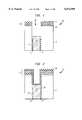
- FIG. 1is a cross-sectional view of a portion of a semiconductor device showing a trench structure
- FIG. 2is a cross-sectional view of the semiconductor device of FIG. 1 having an isolation layer deposited thereon in accordance with the present invention
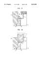
- FIG. 3is cross-sectional view of the semiconductor device of FIG. 2 having a masking layer deposited thereon in accordance with the present invention
- FIG. 4is cross-sectional view of the semiconductor device of FIG. 3 after the masking layer is etched back in accordance with the present invention
- FIG. 5is cross-sectional view of the semiconductor device of FIG. 4 having the isolation layer etched leaving a portion of the isolation layer below the masking layer in accordance with the, present invention
- FIG. 6is cross-sectional view of the semiconductor device of FIG. 5 showing the masking layer removed in accordance with the present invention
- FIG. 7is cross-sectional view of the semiconductor device of FIG. 6 after an isolation trench is etched away in accordance with the present invention
- FIG. 8is cross-sectional view of the semiconductor device of FIG. 7 showing raised shallow trench isolation dielectric formed in the position in accordance with the present invention
- FIG. 9is cross-sectional view of the semiconductor device of FIG. 8 showing a gate stack formed in the trench in accordance with the present invention.
- FIG. 10is cross-sectional view of another embodiment, the semiconductor device of FIG. 2 is shown having a masking layer deposited thereon in accordance with the present invention
- FIG. 11is cross-sectional view of the semiconductor device of FIG. 10 after a position or hole is etched away in accordance with the present invention
- FIG. 12is cross-sectional view of the semiconductor device of FIG. 11 showing shallow trench isolation dielectric formed in the position in accordance with the present invention
- FIG. 13is cross-sectional view of the semiconductor device of FIG. 12 showing a portion of the shallow trench isolation dielectric removed with a portion of the masking layer in accordance with the present invention
- FIG. 14is cross-sectional view of the semiconductor device of FIG. 13 having the isolation layer etched leaving a portion of the isolation layer below the masking layer in accordance with the present invention
- FIG. 15is cross-sectional view of the semiconductor device of FIG. 14 having a pad stack removed in accordance with the present invention.
- FIG. 16is cross-sectional view of the semiconductor device of FIG. 15 showing a gate stack formed in the trench in accordance with the present invention
- FIG. 17is cross-sectional view of another embodiment of the present invention showing a recessed substrate for providing a transistor device that is further away from a trench in accordance with the present invention
- FIG. 18is cross-sectional view of another embodiment of the present invention showing the recessed substrate having a transistor gate and a transistor channel that are further away frog a trench in accordance with the present invention
- FIG. 19is cross-sectional view of a semiconductor device showing two vertical transistors in accordance with the present invention.
- FIG. 20is a schematic view showing the topology of the semiconductor device of FIG. 19.
- This disclosurerelates to semiconductor devices and more particularly, to an apparatus and method for forming deep trench isolation layers for semiconductor memories.
- the present inventionprovides an improved method for forming a top trench isolation layer over a storage node in a deep trench.
- a dummy or masking layeris introduced after deposition of the trench top isolation layer. In this way, the dummy layer may be etched to a desired height.
- the dummy layeris then planarized and recessed in portions leaving a controlled trench top isolation layer portion over the storage node. Further details are included herein.
- FIG. 1shows a portion of a semiconductor device 10.
- Semiconductor device 10includes a substrate 12 preferably a silicon substrate although other materials are contemplated, for example gallium arsenide.
- a deep trench 14is formed in substrate 12 through a pad stack 16 which preferably includes a pad oxide layer 18 and a pad nitride layer 20 by processes known to those skilled in the art.
- Pad oxide layer 18is preferably formed by thermal oxidation although a deposition process may be used.
- Pad nitride layer 20is preferably deposited on pad oxide layer 18.
- a collar 22is formed in trench 14 for electrically isolating a portion of trench 14 from substrate 12.
- a lower portion of trench 14(not shown) is further electrically isolated from substrate 12 by a thin dielectric layer (not shown) about the sides and bottom of trench 14.
- Trench 14is filled with a conductive filler material 24, preferably polysilicon or doped polysilicon. Filler material 24 extends over a top portion of collar 22 and contacts substrate 12. A recess 26 is thereby left in trench 14.
- Isolation layer 28is deposited. Isolation layer 28 coats exposed surfaces including pad stack 16, walls of trench 14 and filler material 24. Isolation layer 28 includes a dielectric material for isolating filler material 24 which functions as a storage node in operation. Filler material 24 between isolation layer 28 and the top of collar 22 is typically called a buried strap 30. Isolation layer 28 preferably includes an oxide, for example silicon oxide, a nitride, for example a silicon nitride, or a combination thereof The deposition of isolation layer 28 results in better control of a thickness of layer 28 by eliminating conventional filling and recessing as performed in the prior art.
- Deposition of isolation layer 28may include chemical vapor deposition (CVD), plasma enhanced chemical vapor deposition (PECVD) or other suitable deposition processes. Such deposition processes are preferred since isolation layer thicknesses are better and more reliably controlled than in the prior art.
- layer 28has a thickness between about 20 nm to about 50 nm, and more preferably between about 30 nm to about 40 nm.
- a dummy or masking layer 32is deposited on the structure shown in FIG. 2.
- Dummy layer 32is preferably polysilicon which advantageously is easier to recess than oxides or nitrides.
- Dummy layer 32may also include a resist.
- Isolation layer 28is selectively etched, preferably by a wet etching process, although dry etching is also contemplated, to remove portions of isolation layer 28 other than the portion masked by dummy layer 32, as shown in FIG. 5.
- Wet etchingmay include etching with HF or HF glycerol. Dry etching may include chemical downstream etching or reactive ion etching.
- pad stack 16is stripped from substrate 12, preferably by a wet etching process.
- Dummy mask 32is optionally etched away, however, depending on the design, dummy mask 32 may be left.
- the remaining structureincludes a controlled trench top isolation layer 34 and is now ready for a sacrificial oxide deposition and ion implantation to form devices on device 10.
- the sacrificial oxide layer(not shown) is removed.
- a conductive material 38is deposited in trench 14.
- a gate oxide 39is formed, followed by a conductive material 38 deposition (part of gate conductor 36).
- Conductive material 38 depositioncan fill or underfill the trench recess.
- a second pad layer 37, preferably nitrideis deposited.
- Device 10is masked (active area) and portions of device 10 are etched to form an isolation trench 29 for raised shallow trench isolation materials.
- a portion of substrate 12, buried strap 30, trench top isolation layer 34, collar 22, filler material 24 and conductive material 38are removed as shown in FIG. 7.
- a dielectric material 40preferably an oxide, is deposited in isolation trenches 29 and planarized to pad layer 37. Pad layer 37 is stripped, followed by the deposition of remaining gate stack layer.
- a gate conductor 36is formed by depositing additional conductive material, preferably includes polysilicon or doped polysilicon.
- a conductive layer 42for example a silicide, such as tungsten silicide, may be deposited on gate conductor 36, to further improve conduction of gate conductor 36.
- Gate conductor 36 and conductive layer 42are isolated by a dielectric material 44 on the top and the sides to form a gate stack.
- Dielectric material 44may include an oxide or a nitride, preferably silicon nitride.
- Gate conductor 36is adjacent to a portion 46 of substrate 12. Portion 46 functions as a channel for a vertical transistor.
- the vertical transistorhas a bitline 210 as a source and a storage node 204 as a drain (See FIG. 19).
- gate conductor 36is separated from buried strap 30 by isolation layer 34.
- isolation layer 34is reliably formed to a predetermined thickness by a deposition process which uses a dummy layer 32 for its formation.
- a thin gate oxide layer 39is disposed between the gate conductor and substrate 12 as is known in the art.
- a dummy or masking layer 32is deposited on the structure of FIG. 2.
- Dummy layer 32covers isolation layer 28.
- Isolation layer 28is substantially the same as described above.
- Dummy layer 32preferably includes polysilicon.
- Dummy layer 32may be deposited having a thickness of between about 20 nm to about 50 nm.
- Dummy layer 32may also be used as an anti-reflection coating (ARC) for subsequent lithographic processes for forming active areas for devices to be formed in later steps.
- ARCanti-reflection coating
- device 100is masked and portions of device 100 are etched to form a position 31 for shallow trench isolation materials.
- a portion of substrate 12, buried strap 30, trench top isolation layer 28, collar 22, filler material 24 and dummy layer 32are removed as shown in FIG. 11.
- position 31is filled with a dielectric material 50, preferably an oxide, such as silicon dioxide.
- a top surface 52is planarized to prepare surface 52 for further processing.
- top surface 52may be deglazed to remove any remaining oxides therefrom.
- Dummy layer 32is recessed to form recess 54 as shown.
- isolation layer 28is selectively etched relative to dummy layer 32.
- a portion of dielectric material 50may be etched as well.
- the etching processpreferably includes wet etching, although dry etching is also contemplated.
- Wet etchingmay include etching with HF or HF glycerol.
- Dry etchingmay include chemical downstream etching or reactive ion etching.
- Dummy layer 32masks a part of isolation layer 28 in contact with buried strap 30 such that a controlled isolation layer 34 is formed.
- pad stack 16is stripped from substrate 12, preferably by a wet etching process.
- Dummy layer 32is optionally etched away prior to the pad oxide strip, however, depending on the design, dummy layer 32 may be left.
- the remaining structureincludes controlled trench top isolation layer 34 and is now ready for a sacrificial oxide deposition and ion implantation to form devices on device 100.
- a gate conductor 36is formed by building a gate stack on top of a conductive material 38.
- Conductive material 38preferably includes polysilicon or doped polysilicon.
- a thin gate oxide layer 39is disposed between the gate conductor and substrate 12 as is known in the art.
- a conductive layer 42for example a silicide, such as tungsten silicide, may be deposited on gate conductor 36, to further improve conduction of gate conductor 36.
- Gate conductor 36 and conductive layer 42are isolated by a dielectric material 44 on the top and the sides.
- Dielectric material 44may include an oxide or a nitride, preferably silicon nitride.
- Gate conductor 36is adjacent to a portion 46 of substrate 12. Portion 46 functions as a channel for a vertical transistor.
- the vertical transistorhas a bitline 210 as a source and a storage node 204 as a drain (See FIG. 19).
- gate conductor 36is separated from buried strap 30 by isolation layer 34.
- isolation layer 34is reliably formed to a predetermined thickness by a deposition process which uses a dummy layer 32 for its formation.
- the structure of FIG. 14may be further processed to achieve improvements for vertical transistors. It is advantageous to move a transistor channel 58 further away from trench 14 to enhance overlap with buried strap outdiffusion without impacting device performance by formation of deep junctions.
- An etching processis preferably performed to remove a portion 60 of substrate 12 such that when channel 58 is formed, channel 58 is further away from trench 14.
- dummy layer 32may also be etched.
- the etching processpreferably includes dry etching, for example chemical downstream etching.
- Substrate 12is etched such that a recess 60 is formed. As shown in FIG. 18, recess 60 provides room for a vertical transistor 62 (bounded by dashed lines) to be moved further away from trench 14.
- a thin gate oxide layer 39is disposed between the gate conductor and substrate 12 as is known in the art.
- a semiconductor memory 200is shown having two memory cells in accordance with the present invention.
- Each memory cellincludes buried strap 30 having isolation layer 34 formed thereon in accordance with the methods of the present invention.
- Buried strap 30includes an outdiffusion region 202 which assists in connecting channels 58 to a storage node 204 within trench 14.
- a doped region 206joins channels 58 to a bitline contact 208 which connects to a bitline 210.
- Bitline 210acts as a source for vertical transistor 212 while storage node 204 acts as a drain.
- a gate 214is activated allowing current to flow between bitline 210 and storage node 204.
- Isolation layer 34separates gate conductor 36 from storage node 204.
- a thin gate oxide layer 39is disposed between the gate conductor and substrate 12 as is known in the art.
- a dielectric layer 216isolates bitline 210.
- Dielectric layer 216preferably includes an oxide, such as borophosphosilicate glass (BPSG).
Landscapes
- Engineering & Computer Science (AREA)
- Manufacturing & Machinery (AREA)
- Physics & Mathematics (AREA)
- Condensed Matter Physics & Semiconductors (AREA)
- General Physics & Mathematics (AREA)
- Computer Hardware Design (AREA)
- Microelectronics & Electronic Packaging (AREA)
- Power Engineering (AREA)
- Semiconductor Memories (AREA)
- Element Separation (AREA)
- Non-Volatile Memory (AREA)
Abstract
Description
Claims (25)
Priority Applications (7)
| Application Number | Priority Date | Filing Date | Title |
|---|---|---|---|
| US09/127,262US6074909A (en) | 1998-07-31 | 1998-07-31 | Apparatus and method for forming controlled deep trench top isolation layers |
| EP99113538AEP0977256A3 (en) | 1998-07-31 | 1999-07-06 | Method of forming DRAM trench capacitor |
| TW088112385ATW425654B (en) | 1998-07-31 | 1999-07-21 | Apparatus and method for forming controlled deep trench top isolation layers |
| JP11214006AJP2000058778A (en) | 1998-07-31 | 1999-07-28 | Method for forming a deep trench top insulating layer and semiconductor memory according to the method |
| CNB991118685ACN1165984C (en) | 1998-07-31 | 1999-07-30 | Apparatus and method for forming controlled deep trench top isolation layer |
| KR1019990031507AKR100555599B1 (en) | 1998-07-31 | 1999-07-31 | Apparatus and method for forming controlled deep trench top isolation layers |
| US09/503,992US6359299B1 (en) | 1998-07-31 | 2000-02-14 | Apparatus and method for forming controlled deep trench top isolation layers |
Applications Claiming Priority (1)
| Application Number | Priority Date | Filing Date | Title |
|---|---|---|---|
| US09/127,262US6074909A (en) | 1998-07-31 | 1998-07-31 | Apparatus and method for forming controlled deep trench top isolation layers |
Related Child Applications (1)
| Application Number | Title | Priority Date | Filing Date |
|---|---|---|---|
| US09/503,992DivisionUS6359299B1 (en) | 1998-07-31 | 2000-02-14 | Apparatus and method for forming controlled deep trench top isolation layers |
Publications (1)
| Publication Number | Publication Date |
|---|---|
| US6074909Atrue US6074909A (en) | 2000-06-13 |
Family
ID=22429184
Family Applications (2)
| Application Number | Title | Priority Date | Filing Date |
|---|---|---|---|
| US09/127,262Expired - LifetimeUS6074909A (en) | 1998-07-31 | 1998-07-31 | Apparatus and method for forming controlled deep trench top isolation layers |
| US09/503,992Expired - LifetimeUS6359299B1 (en) | 1998-07-31 | 2000-02-14 | Apparatus and method for forming controlled deep trench top isolation layers |
Family Applications After (1)
| Application Number | Title | Priority Date | Filing Date |
|---|---|---|---|
| US09/503,992Expired - LifetimeUS6359299B1 (en) | 1998-07-31 | 2000-02-14 | Apparatus and method for forming controlled deep trench top isolation layers |
Country Status (6)
| Country | Link |
|---|---|
| US (2) | US6074909A (en) |
| EP (1) | EP0977256A3 (en) |
| JP (1) | JP2000058778A (en) |
| KR (1) | KR100555599B1 (en) |
| CN (1) | CN1165984C (en) |
| TW (1) | TW425654B (en) |
Cited By (33)
| Publication number | Priority date | Publication date | Assignee | Title |
|---|---|---|---|---|
| US6184107B1 (en)* | 1999-03-17 | 2001-02-06 | International Business Machines Corp. | Capacitor trench-top dielectric for self-aligned device isolation |
| US6190971B1 (en)* | 1999-05-13 | 2001-02-20 | International Business Machines Corporation | Formation of 5F2 cell with partially vertical transistor and gate conductor aligned buried strap with raised shallow trench isolation region |
| US6204140B1 (en)* | 1999-03-24 | 2001-03-20 | Infineon Technologies North America Corp. | Dynamic random access memory |
| US6228705B1 (en)* | 1999-02-03 | 2001-05-08 | International Business Machines Corporation | Overlay process for fabricating a semiconductor device |
| US6255683B1 (en)* | 1998-12-29 | 2001-07-03 | Infineon Technologies Ag | Dynamic random access memory |
| US6288422B1 (en)* | 2000-03-31 | 2001-09-11 | International Business Machines Corporation | Structure and process for fabricating a 6F2 DRAM cell having vertical MOSFET and large trench capacitance |
| US6291298B1 (en)* | 1999-05-25 | 2001-09-18 | Advanced Analogic Technologies, Inc. | Process of manufacturing Trench gate semiconductor device having gate oxide layer with multiple thicknesses |
| US6316805B1 (en)* | 2000-01-06 | 2001-11-13 | Vanguard International Semiconductor Corporation | Electrostatic discharge device with gate-controlled field oxide transistor |
| US6326275B1 (en)* | 2000-04-24 | 2001-12-04 | International Business Machines Corporation | DRAM cell with vertical CMOS transistor |
| US6339241B1 (en)* | 2000-06-23 | 2002-01-15 | International Business Machines Corporation | Structure and process for 6F2 trench capacitor DRAM cell with vertical MOSFET and 3F bitline pitch |
| US6355518B1 (en)* | 2000-09-05 | 2002-03-12 | Promos Technologies, Inc. | Method for making a DRAM cell with deep-trench capacitors and overlying vertical transistors |
| US6368912B1 (en)* | 2000-12-08 | 2002-04-09 | Nanya Technology Corporation | Method of fabricating an isolation structure between a vertical transistor and a deep trench capacitor |
| US6372573B2 (en)* | 1999-10-26 | 2002-04-16 | Kabushiki Kaisha Toshiba | Self-aligned trench capacitor capping process for high density DRAM cells |
| US6399435B1 (en)* | 1999-02-19 | 2002-06-04 | Infineon Technologies Ag | Method for producing a DRAM cell with a trench capacitor |
| US6399447B1 (en)* | 2000-07-19 | 2002-06-04 | International Business Machines Corporation | Method of producing dynamic random access memory (DRAM) cell with folded bitline vertical transistor |
| US6420750B1 (en)* | 1999-02-22 | 2002-07-16 | International Business Machines Corporation | Structure and method for buried-strap with reduced outdiffusion |
| US6441422B1 (en)* | 2000-11-03 | 2002-08-27 | International Business Machines Corporation | Structure and method for ultra-scalable hybrid DRAM cell with contacted P-well |
| US6458647B1 (en)* | 2001-08-27 | 2002-10-01 | Infineon Technologies Ag | Process flow for sacrificial collar with poly mask |
| US6509226B1 (en)* | 2000-09-27 | 2003-01-21 | International Business Machines Corporation | Process for protecting array top oxide |
| US6514817B1 (en)* | 2001-09-25 | 2003-02-04 | Promos Technologies Inc. | Method of forming shallow trench |
| US20030032248A1 (en)* | 2001-08-10 | 2003-02-13 | Christiana Yue | Method of fabricating trench MIS device with graduated gate oxide layer |
| US6541810B2 (en)* | 2001-06-29 | 2003-04-01 | International Business Machines Corporation | Modified vertical MOSFET and methods of formation thereof |
| US6586300B1 (en)* | 2002-04-18 | 2003-07-01 | Infineon Technologies Ag | Spacer assisted trench top isolation for vertical DRAM's |
| DE10212610C1 (en)* | 2002-03-21 | 2003-11-06 | Infineon Technologies Ag | Producing horizontal insulation layer on conducting material in trench, deposits insulant layer over trench- and sidewall structures, followed by controlled removal |
| US20040038467A1 (en)* | 2001-07-03 | 2004-02-26 | Siliconix Incorporated | Trench MIS device having implanted drain-drift region and thick bottom oxide and process for manufacturing the same |
| US20040038481A1 (en)* | 2001-07-03 | 2004-02-26 | Siliconix Incorporated | Trench MOSFET having implanted drain-drift region and process for manufacturing the same |
| US20040063300A1 (en)* | 2002-10-01 | 2004-04-01 | Taiwan Semiconductor Manufacturing Company | Shallow trench filled with two or more dielectrics for isolation and coupling or for stress control |
| US20040166636A1 (en)* | 2001-07-03 | 2004-08-26 | Siliconix Incorporated | Trench MIS device with thick oxide layer in bottom of gate contact trench |
| US20050236665A1 (en)* | 2001-07-03 | 2005-10-27 | Darwish Mohamed N | Trench MIS device having implanted drain-drift region and thick bottom oxide and process for manufacturing the same |
| US20060038223A1 (en)* | 2001-07-03 | 2006-02-23 | Siliconix Incorporated | Trench MOSFET having drain-drift region comprising stack of implanted regions |
| US20060189070A1 (en)* | 2005-02-21 | 2006-08-24 | Masaru Kidoh | Semiconductor device and method of manufacturing the same |
| US20070131998A1 (en)* | 2005-11-03 | 2007-06-14 | Nanya Technology Corporation | Vertical transistor device and fabrication method thereof |
| US20080258268A1 (en)* | 2007-04-18 | 2008-10-23 | International Business Machines Corporation | Trench structure and method of forming the trench structure |
Families Citing this family (8)
| Publication number | Priority date | Publication date | Assignee | Title |
|---|---|---|---|---|
| TW469635B (en)* | 2000-05-16 | 2001-12-21 | Nanya Technology Corp | Fabrication method of semiconductor memory cell transistor |
| US6610573B2 (en) | 2001-06-22 | 2003-08-26 | Infineon Technologies Ag | Method for forming a single wiring level for transistors with planar and vertical gates on the same substrate |
| US6913941B2 (en)* | 2002-09-09 | 2005-07-05 | Freescale Semiconductor, Inc. | SOI polysilicon trench refill perimeter oxide anchor scheme |
| US6830968B1 (en)* | 2003-07-16 | 2004-12-14 | International Business Machines Corporation | Simplified top oxide late process |
| JP2007194267A (en)* | 2006-01-17 | 2007-08-02 | Toshiba Corp | Semiconductor memory device |
| KR101116335B1 (en)* | 2009-12-30 | 2012-03-14 | 주식회사 하이닉스반도체 | Semiconductor device with buried bitline and method for manufacturing the same |
| US8299562B2 (en)* | 2011-03-28 | 2012-10-30 | Nanya Technology Corporation | Isolation structure and device structure including the same |
| CN106366152B (en)* | 2016-08-25 | 2018-01-19 | 桂林益天成生物科技有限公司 | The method that asiaticosid is extracted from centella |
Citations (2)
| Publication number | Priority date | Publication date | Assignee | Title |
|---|---|---|---|---|
| US5482883A (en)* | 1993-12-01 | 1996-01-09 | International Business Machines Corporation | Method for fabricating low leakage substrate plate trench DRAM cells and devices formed thereby |
| US5831301A (en)* | 1998-01-28 | 1998-11-03 | International Business Machines Corp. | Trench storage dram cell including a step transfer device |
Family Cites Families (32)
| Publication number | Priority date | Publication date | Assignee | Title |
|---|---|---|---|---|
| US5225697A (en)* | 1984-09-27 | 1993-07-06 | Texas Instruments, Incorporated | dRAM cell and method |
| JPH0680805B2 (en)* | 1985-05-29 | 1994-10-12 | 日本電気株式会社 | MIS type semiconductor memory device |
| JPH0760859B2 (en)* | 1985-11-19 | 1995-06-28 | 沖電気工業株式会社 | Semiconductor device and manufacturing method thereof |
| US4769786A (en)* | 1986-07-15 | 1988-09-06 | International Business Machines Corporation | Two square memory cells |
| JPS63211750A (en)* | 1987-02-27 | 1988-09-02 | Mitsubishi Electric Corp | semiconductor storage device |
| US4916524A (en)* | 1987-03-16 | 1990-04-10 | Texas Instruments Incorporated | Dram cell and method |
| JPS63245954A (en)* | 1987-04-01 | 1988-10-13 | Hitachi Ltd | semiconductor memory |
| US4942554A (en)* | 1987-11-26 | 1990-07-17 | Siemens Aktiengesellschaft | Three-dimensional, one-transistor cell arrangement for dynamic semiconductor memories comprising trench capacitor and method for manufacturing same |
| JPH02158134A (en)* | 1988-12-12 | 1990-06-18 | Sony Corp | Manufacturing method of semiconductor device |
| US4945069A (en)* | 1988-12-16 | 1990-07-31 | Texas Instruments, Incorporated | Organic space holder for trench processing |
| JPH0414868A (en)* | 1990-05-09 | 1992-01-20 | Hitachi Ltd | Semiconductor memory and manufacture thereof |
| US4988637A (en)* | 1990-06-29 | 1991-01-29 | International Business Machines Corp. | Method for fabricating a mesa transistor-trench capacitor memory cell structure |
| KR940006679B1 (en)* | 1991-09-26 | 1994-07-25 | 현대전자산업 주식회사 | Dram cell having a vertical transistor and fabricating method thereof |
| US5185294A (en)* | 1991-11-22 | 1993-02-09 | International Business Machines Corporation | Boron out-diffused surface strap process |
| US5262346A (en)* | 1992-12-16 | 1993-11-16 | International Business Machines Corporation | Nitride polish stop for forming SOI wafers |
| US5363327A (en)* | 1993-01-19 | 1994-11-08 | International Business Machines Corporation | Buried-sidewall-strap two transistor one capacitor trench cell |
| US5422294A (en)* | 1993-05-03 | 1995-06-06 | Noble, Jr.; Wendell P. | Method of making a trench capacitor field shield with sidewall contact |
| JPH0758214A (en)* | 1993-08-13 | 1995-03-03 | Toshiba Corp | Semiconductor memory device |
| US5360758A (en)* | 1993-12-03 | 1994-11-01 | International Business Machines Corporation | Self-aligned buried strap for trench type DRAM cells |
| US5369049A (en)* | 1993-12-17 | 1994-11-29 | International Business Machines Corporation | DRAM cell having raised source, drain and isolation |
| US5395786A (en)* | 1994-06-30 | 1995-03-07 | International Business Machines Corporation | Method of making a DRAM cell with trench capacitor |
| US5627092A (en)* | 1994-09-26 | 1997-05-06 | Siemens Aktiengesellschaft | Deep trench dram process on SOI for low leakage DRAM cell |
| US5936271A (en)* | 1994-11-15 | 1999-08-10 | Siemens Aktiengesellschaft | Unit cell layout and transfer gate design for high density DRAMs having a trench capacitor with signal electrode composed of three differently doped polysilicon layers |
| US5895255A (en)* | 1994-11-30 | 1999-04-20 | Kabushiki Kaisha Toshiba | Shallow trench isolation formation with deep trench cap |
| US5545583A (en)* | 1995-04-13 | 1996-08-13 | International Business Machines Corporation | Method of making semiconductor trench capacitor cell having a buried strap |
| US5576566A (en)* | 1995-04-13 | 1996-11-19 | International Business Machines Corporation | Semiconductor trench capacitor cell having a buried strap |
| US5614431A (en)* | 1995-12-20 | 1997-03-25 | International Business Machines Corporation | Method of making buried strap trench cell yielding an extended transistor |
| US5937296A (en)* | 1996-12-20 | 1999-08-10 | Siemens Aktiengesellschaft | Memory cell that includes a vertical transistor and a trench capacitor |
| US5981332A (en)* | 1997-09-30 | 1999-11-09 | Siemens Aktiengesellschaft | Reduced parasitic leakage in semiconductor devices |
| US6025230A (en)* | 1997-11-06 | 2000-02-15 | Mageposer Semiconductor Corporation | High speed MOSFET power device with enhanced ruggedness fabricated by simplified processes |
| US6080618A (en)* | 1998-03-31 | 2000-06-27 | Siemens Aktiengesellschaft | Controllability of a buried device layer |
| US6066527A (en)* | 1999-07-26 | 2000-05-23 | Infineon Technologies North America Corp. | Buried strap poly etch back (BSPE) process |
- 1998
- 1998-07-31USUS09/127,262patent/US6074909A/ennot_activeExpired - Lifetime
- 1999
- 1999-07-06EPEP99113538Apatent/EP0977256A3/ennot_activeWithdrawn
- 1999-07-21TWTW088112385Apatent/TW425654B/ennot_activeIP Right Cessation
- 1999-07-28JPJP11214006Apatent/JP2000058778A/ennot_activeWithdrawn
- 1999-07-30CNCNB991118685Apatent/CN1165984C/ennot_activeExpired - Fee Related
- 1999-07-31KRKR1019990031507Apatent/KR100555599B1/ennot_activeExpired - Fee Related
- 2000
- 2000-02-14USUS09/503,992patent/US6359299B1/ennot_activeExpired - Lifetime
Patent Citations (2)
| Publication number | Priority date | Publication date | Assignee | Title |
|---|---|---|---|---|
| US5482883A (en)* | 1993-12-01 | 1996-01-09 | International Business Machines Corporation | Method for fabricating low leakage substrate plate trench DRAM cells and devices formed thereby |
| US5831301A (en)* | 1998-01-28 | 1998-11-03 | International Business Machines Corp. | Trench storage dram cell including a step transfer device |
Cited By (71)
| Publication number | Priority date | Publication date | Assignee | Title |
|---|---|---|---|---|
| US6255683B1 (en)* | 1998-12-29 | 2001-07-03 | Infineon Technologies Ag | Dynamic random access memory |
| US6228705B1 (en)* | 1999-02-03 | 2001-05-08 | International Business Machines Corporation | Overlay process for fabricating a semiconductor device |
| US6399435B1 (en)* | 1999-02-19 | 2002-06-04 | Infineon Technologies Ag | Method for producing a DRAM cell with a trench capacitor |
| US6420750B1 (en)* | 1999-02-22 | 2002-07-16 | International Business Machines Corporation | Structure and method for buried-strap with reduced outdiffusion |
| US6184107B1 (en)* | 1999-03-17 | 2001-02-06 | International Business Machines Corp. | Capacitor trench-top dielectric for self-aligned device isolation |
| US6204140B1 (en)* | 1999-03-24 | 2001-03-20 | Infineon Technologies North America Corp. | Dynamic random access memory |
| US6399978B2 (en) | 1999-05-13 | 2002-06-04 | International Business Machines Corp. | Formation of 5F2 cell with partially vertical transistor and gate conductor aligned buried strap with raised shallow trench isolation region |
| US6190971B1 (en)* | 1999-05-13 | 2001-02-20 | International Business Machines Corporation | Formation of 5F2 cell with partially vertical transistor and gate conductor aligned buried strap with raised shallow trench isolation region |
| US7238568B2 (en) | 1999-05-25 | 2007-07-03 | Advanced Analogic Technologies, Inc. | Trench semiconductor device having gate oxide layer with multiple thicknesses and processes of fabricating the same |
| US7282412B2 (en) | 1999-05-25 | 2007-10-16 | Advanced Analogic Technologies, Inc. | Trench semiconductor device having gate oxide layer with multiple thicknesses and processes of fabricating the same |
| US20040203200A1 (en)* | 1999-05-25 | 2004-10-14 | Advanced Analogic Technologies, Inc. | Trench semiconductor device having gate oxide layer with mulitiple thicknesses and processes of fabricating the same |
| US6900100B2 (en) | 1999-05-25 | 2005-05-31 | Advanced Analogic Technologies, Inc. | Trench semiconductor device having gate oxide layer with multiple thicknesses and processes of fabricating the same |
| US20050215013A1 (en)* | 1999-05-25 | 2005-09-29 | Advanced Analogic Technologies, Inc. | Trench semiconductor device having gate oxide layer with mulitiple thicknesses and processes of fabricating the same |
| US20050215012A1 (en)* | 1999-05-25 | 2005-09-29 | Advanced Analogic Technologies, Inc. | Trench semiconductor device having gate oxide layer with multiple thicknesses and processes of fabricating the same |
| US20050215027A1 (en)* | 1999-05-25 | 2005-09-29 | Advanced Analogic Technologies, Inc. | Trench semiconductor device having gate oxide layer with multiple thicknesses and processes of fabricating the same |
| US6291298B1 (en)* | 1999-05-25 | 2001-09-18 | Advanced Analogic Technologies, Inc. | Process of manufacturing Trench gate semiconductor device having gate oxide layer with multiple thicknesses |
| US7276411B2 (en) | 1999-05-25 | 2007-10-02 | Advanced Analogic Technologies, Inc. | Trench semiconductor device having gate oxide layer with multiple thicknesses and processes of fabricating the same |
| US6372573B2 (en)* | 1999-10-26 | 2002-04-16 | Kabushiki Kaisha Toshiba | Self-aligned trench capacitor capping process for high density DRAM cells |
| US6316805B1 (en)* | 2000-01-06 | 2001-11-13 | Vanguard International Semiconductor Corporation | Electrostatic discharge device with gate-controlled field oxide transistor |
| US6288422B1 (en)* | 2000-03-31 | 2001-09-11 | International Business Machines Corporation | Structure and process for fabricating a 6F2 DRAM cell having vertical MOSFET and large trench capacitance |
| US6326275B1 (en)* | 2000-04-24 | 2001-12-04 | International Business Machines Corporation | DRAM cell with vertical CMOS transistor |
| US6339241B1 (en)* | 2000-06-23 | 2002-01-15 | International Business Machines Corporation | Structure and process for 6F2 trench capacitor DRAM cell with vertical MOSFET and 3F bitline pitch |
| US6630379B2 (en) | 2000-06-23 | 2003-10-07 | International Business Machines Corporation | Method of manufacturing 6F2 trench capacitor DRAM cell having vertical MOSFET and 3F bitline pitch |
| US6720602B2 (en) | 2000-07-19 | 2004-04-13 | International Business Machines Corporation | Dynamic random access memory (DRAM) cell with folded bitline vertical transistor and method of producing the same |
| US6399447B1 (en)* | 2000-07-19 | 2002-06-04 | International Business Machines Corporation | Method of producing dynamic random access memory (DRAM) cell with folded bitline vertical transistor |
| US6355518B1 (en)* | 2000-09-05 | 2002-03-12 | Promos Technologies, Inc. | Method for making a DRAM cell with deep-trench capacitors and overlying vertical transistors |
| US6509226B1 (en)* | 2000-09-27 | 2003-01-21 | International Business Machines Corporation | Process for protecting array top oxide |
| US6441422B1 (en)* | 2000-11-03 | 2002-08-27 | International Business Machines Corporation | Structure and method for ultra-scalable hybrid DRAM cell with contacted P-well |
| US6368912B1 (en)* | 2000-12-08 | 2002-04-09 | Nanya Technology Corporation | Method of fabricating an isolation structure between a vertical transistor and a deep trench capacitor |
| US6541810B2 (en)* | 2001-06-29 | 2003-04-01 | International Business Machines Corporation | Modified vertical MOSFET and methods of formation thereof |
| US20040166636A1 (en)* | 2001-07-03 | 2004-08-26 | Siliconix Incorporated | Trench MIS device with thick oxide layer in bottom of gate contact trench |
| US7435650B2 (en) | 2001-07-03 | 2008-10-14 | Siliconix Incorporated | Process for manufacturing trench MIS device having implanted drain-drift region and thick bottom oxide |
| US6764906B2 (en) | 2001-07-03 | 2004-07-20 | Siliconix Incorporated | Method for making trench mosfet having implanted drain-drift region |
| US7291884B2 (en) | 2001-07-03 | 2007-11-06 | Siliconix Incorporated | Trench MIS device having implanted drain-drift region and thick bottom oxide |
| US20040038481A1 (en)* | 2001-07-03 | 2004-02-26 | Siliconix Incorporated | Trench MOSFET having implanted drain-drift region and process for manufacturing the same |
| US20040227182A1 (en)* | 2001-07-03 | 2004-11-18 | Siliconix Incorporated | Process for manufacturing trench MIS device having implanted drain-drift region and thick botton oxide |
| US20060121676A1 (en)* | 2001-07-03 | 2006-06-08 | Siliconix Incorporated | Trench MIS device with thick oxide layer in bottom of gate contact trench |
| US20050236665A1 (en)* | 2001-07-03 | 2005-10-27 | Darwish Mohamed N | Trench MIS device having implanted drain-drift region and thick bottom oxide and process for manufacturing the same |
| US7033876B2 (en) | 2001-07-03 | 2006-04-25 | Siliconix Incorporated | Trench MIS device having implanted drain-drift region and thick bottom oxide and process for manufacturing the same |
| US7326995B2 (en) | 2001-07-03 | 2008-02-05 | Siliconix Incorporated | Trench MIS device having implanted drain-drift region and thick bottom oxide |
| US20040038467A1 (en)* | 2001-07-03 | 2004-02-26 | Siliconix Incorporated | Trench MIS device having implanted drain-drift region and thick bottom oxide and process for manufacturing the same |
| US7009247B2 (en) | 2001-07-03 | 2006-03-07 | Siliconix Incorporated | Trench MIS device with thick oxide layer in bottom of gate contact trench |
| US20060038223A1 (en)* | 2001-07-03 | 2006-02-23 | Siliconix Incorporated | Trench MOSFET having drain-drift region comprising stack of implanted regions |
| US7416947B2 (en) | 2001-07-03 | 2008-08-26 | Siliconix Incorporated | Method of fabricating trench MIS device with thick oxide layer in bottom of trench |
| US6903412B2 (en) | 2001-08-10 | 2005-06-07 | Siliconix Incorporated | Trench MIS device with graduated gate oxide layer |
| US20030030104A1 (en)* | 2001-08-10 | 2003-02-13 | Darwish Mohamed N. | Trench MIS device with graduated gate oxide layer |
| US20030032248A1 (en)* | 2001-08-10 | 2003-02-13 | Christiana Yue | Method of fabricating trench MIS device with graduated gate oxide layer |
| US6875657B2 (en) | 2001-08-10 | 2005-04-05 | Siliconix Incorporated | Method of fabricating trench MIS device with graduated gate oxide layer |
| US6849898B2 (en) | 2001-08-10 | 2005-02-01 | Siliconix Incorporated | Trench MIS device with active trench corners and thick bottom oxide |
| US6458647B1 (en)* | 2001-08-27 | 2002-10-01 | Infineon Technologies Ag | Process flow for sacrificial collar with poly mask |
| US6514817B1 (en)* | 2001-09-25 | 2003-02-04 | Promos Technologies Inc. | Method of forming shallow trench |
| DE10212610C1 (en)* | 2002-03-21 | 2003-11-06 | Infineon Technologies Ag | Producing horizontal insulation layer on conducting material in trench, deposits insulant layer over trench- and sidewall structures, followed by controlled removal |
| US6825079B2 (en) | 2002-03-21 | 2004-11-30 | Infineon Technologies Ag | Method for producing a horizontal insulation layer on a conductive material in a trench |
| US20040043560A1 (en)* | 2002-03-21 | 2004-03-04 | Martin Popp | Method for producing a horizontal insulation layer on a conductive material in a trench |
| DE10317601B4 (en)* | 2002-04-18 | 2008-04-03 | Infineon Technologies Ag | Method for producing a vertical DRAM device |
| US6586300B1 (en)* | 2002-04-18 | 2003-07-01 | Infineon Technologies Ag | Spacer assisted trench top isolation for vertical DRAM's |
| US6828211B2 (en) | 2002-10-01 | 2004-12-07 | Taiwan Semiconductor Manufacturing Co., Ltd. | Shallow trench filled with two or more dielectrics for isolation and coupling or for stress control |
| US20060121394A1 (en)* | 2002-10-01 | 2006-06-08 | Taiwan Semiconductor Manufacturing Co., Ltd. | Shallow trench filled with two or more dielectrics for isolation and coupling for stress control |
| US7320926B2 (en) | 2002-10-01 | 2008-01-22 | Taiwan Semiconductor Manufacturing Co., Ltd. | Shallow trench filled with two or more dielectrics for isolation and coupling for stress control |
| US7018886B2 (en) | 2002-10-01 | 2006-03-28 | Taiwan Semiconductor Manufacturing Co., Ltd. | Shallow trench filled with two or more dielectrics for isolation and coupling or for stress control |
| US20040063300A1 (en)* | 2002-10-01 | 2004-04-01 | Taiwan Semiconductor Manufacturing Company | Shallow trench filled with two or more dielectrics for isolation and coupling or for stress control |
| US7145197B2 (en)* | 2005-02-21 | 2006-12-05 | Kabushiki Kaisha Toshiba | Semiconductor device and method of manufacturing the same |
| US20060189070A1 (en)* | 2005-02-21 | 2006-08-24 | Masaru Kidoh | Semiconductor device and method of manufacturing the same |
| US20070131998A1 (en)* | 2005-11-03 | 2007-06-14 | Nanya Technology Corporation | Vertical transistor device and fabrication method thereof |
| US7808028B2 (en) | 2007-04-18 | 2010-10-05 | International Business Machines Corporation | Trench structure and method of forming trench structure |
| WO2008131234A1 (en)* | 2007-04-18 | 2008-10-30 | International Business Machines Corporation | A trench structure and method of forming the trench structure |
| US20080258268A1 (en)* | 2007-04-18 | 2008-10-23 | International Business Machines Corporation | Trench structure and method of forming the trench structure |
| US20100252873A1 (en)* | 2007-04-18 | 2010-10-07 | International Business Machines Corporation | Trench structure and method of forming the trench structure |
| US8236644B2 (en) | 2007-04-18 | 2012-08-07 | International Business Machines Corporation | Trench structure and method of forming the trench structure |
| CN101657884B (en)* | 2007-04-18 | 2013-01-02 | 国际商业机器公司 | Trench structure and method of forming the trench structure |
| US8680598B2 (en) | 2007-04-18 | 2014-03-25 | International Business Machines Corporation | Trench structure and method of forming the trench structure |
Also Published As
| Publication number | Publication date |
|---|---|
| CN1244036A (en) | 2000-02-09 |
| EP0977256A3 (en) | 2005-12-14 |
| TW425654B (en) | 2001-03-11 |
| KR100555599B1 (en) | 2006-03-03 |
| JP2000058778A (en) | 2000-02-25 |
| EP0977256A2 (en) | 2000-02-02 |
| CN1165984C (en) | 2004-09-08 |
| US6359299B1 (en) | 2002-03-19 |
| KR20000012124A (en) | 2000-02-25 |
Similar Documents
| Publication | Publication Date | Title |
|---|---|---|
| US6074909A (en) | Apparatus and method for forming controlled deep trench top isolation layers | |
| US6177698B1 (en) | Formation of controlled trench top isolation layers for vertical transistors | |
| KR100431656B1 (en) | Method of manufacturing semiconductor device | |
| US6008084A (en) | Method for fabricating low resistance bit line structures, along with bit line structures exhibiting low bit line to bit line coupling capacitance | |
| US5933748A (en) | Shallow trench isolation process | |
| US6204140B1 (en) | Dynamic random access memory | |
| US6576944B2 (en) | Self-aligned nitride pattern for improved process window | |
| US6222218B1 (en) | DRAM trench | |
| US5717628A (en) | Nitride cap formation in a DRAM trench capacitor | |
| KR100474150B1 (en) | Fully encapsulated damascene gates for gigabit drams | |
| US20030162353A1 (en) | Method for fabricating semiconductor device, and semiconductor device, having storage node contact plugs | |
| US6599798B2 (en) | Method of preparing buried LOCOS collar in trench DRAMS | |
| US6274426B1 (en) | Self-aligned contact process for a crown shaped dynamic random access memory capacitor structure | |
| US6271080B1 (en) | Structure and method for planar MOSFET DRAM cell free of wordline gate conductor to storage trench overlay sensitivity | |
| US6960523B2 (en) | Method of reducing erosion of a nitride gate cap layer during reactive ion etch of nitride liner layer for bit line contact of DRAM device | |
| US6229173B1 (en) | Hybrid 5F2 cell layout for buried surface strap aligned to vertical transistor | |
| US6074955A (en) | Method of fabricating a node contact window of DRAM | |
| US6136716A (en) | Method for manufacturing a self-aligned stacked storage node DRAM cell | |
| US6909136B2 (en) | Trench-capacitor DRAM cell having a folded gate conductor | |
| US6964898B1 (en) | Method for fabricating deep trench capacitor | |
| KR100536042B1 (en) | Method for forming recess gate electrode in semiconductor process | |
| US6033966A (en) | Method for making an 8-shaped storage node DRAM cell | |
| JPH11330402A (en) | Method of controlling dispersion in embedded straps of trench capacitors | |
| HK1022565A (en) | Method of forming dram trench capacitor | |
| KR20040016496A (en) | Method for forming spacer of semiconductor device and manufacturing semiconductor device using the same |
Legal Events
| Date | Code | Title | Description |
|---|---|---|---|
| AS | Assignment | Owner name:SIEMENS MICROELECTRONICS, INC., CALIFORNIA Free format text:ASSIGNMENT OF ASSIGNORS INTEREST;ASSIGNOR:GRUENING, ULRIKE;REEL/FRAME:009372/0016 Effective date:19980727 | |
| AS | Assignment | Owner name:SIEMENS AKTIENGESELLSCHAFT, GERMANY Free format text:ASSIGNMENT OF ASSIGNORS INTEREST;ASSIGNOR:SIEMENS MICROELECTRONICS, INC.;REEL/FRAME:009891/0917 Effective date:19990316 | |
| STCF | Information on status: patent grant | Free format text:PATENTED CASE | |
| FEPP | Fee payment procedure | Free format text:PAYOR NUMBER ASSIGNED (ORIGINAL EVENT CODE: ASPN); ENTITY STATUS OF PATENT OWNER: LARGE ENTITY | |
| FPAY | Fee payment | Year of fee payment:4 | |
| FPAY | Fee payment | Year of fee payment:8 | |
| AS | Assignment | Owner name:INFINEON TECHNOLOGIES AG,GERMANY Free format text:ASSIGNMENT OF ASSIGNORS INTEREST;ASSIGNOR:SIEMENS AKTIENGESELLSCHAFT;REEL/FRAME:024114/0059 Effective date:19990331 | |
| AS | Assignment | Owner name:QIMONDA AG,GERMANY Free format text:ASSIGNMENT OF ASSIGNORS INTEREST;ASSIGNOR:INFINEON TECHNOLOGIES AG;REEL/FRAME:024218/0001 Effective date:20060425 | |
| FPAY | Fee payment | Year of fee payment:12 | |
| AS | Assignment | Owner name:INFINEON TECHNOLOGIES AG, GERMANY Free format text:ASSIGNMENT OF ASSIGNORS INTEREST;ASSIGNOR:QIMONDA AG;REEL/FRAME:035623/0001 Effective date:20141009 | |
| AS | Assignment | Owner name:POLARIS INNOVATIONS LIMITED, IRELAND Free format text:ASSIGNMENT OF ASSIGNORS INTEREST;ASSIGNOR:INFINEON TECHNOLOGIES AG;REEL/FRAME:036353/0134 Effective date:20150708 |