US6074896A - Method of processing semiconductor material wafers and method of forming flip chips and semiconductor chips - Google Patents
Method of processing semiconductor material wafers and method of forming flip chips and semiconductor chipsDownload PDFInfo
- Publication number
- US6074896A US6074896AUS09/235,567US23556799AUS6074896AUS 6074896 AUS6074896 AUS 6074896AUS 23556799 AUS23556799 AUS 23556799AUS 6074896 AUS6074896 AUS 6074896A
- Authority
- US
- United States
- Prior art keywords
- wafer
- cut
- semiconductor wafer
- cutting
- insulative material
- Prior art date
- Legal status (The legal status is an assumption and is not a legal conclusion. Google has not performed a legal analysis and makes no representation as to the accuracy of the status listed.)
- Expired - Lifetime
Links
- 239000000463materialSubstances0.000titleclaimsabstractdescription62
- 238000000034methodMethods0.000titleclaimsabstractdescription52
- 239000004065semiconductorSubstances0.000titleclaimsabstractdescription40
- 238000012545processingMethods0.000titleclaimsabstractdescription33
- 235000012431wafersNutrition0.000titledescription61
- 238000005520cutting processMethods0.000claimsabstractdescription53
- 238000000151depositionMethods0.000claimsabstract3
- 238000000059patterningMethods0.000claims1
- 239000011810insulating materialSubstances0.000abstractdescription20
- 239000010408filmSubstances0.000description14
- 239000000853adhesiveSubstances0.000description8
- 230000001070adhesive effectEffects0.000description8
- 239000002313adhesive filmSubstances0.000description4
- 239000002184metalSubstances0.000description4
- 239000004020conductorSubstances0.000description2
- 239000012634fragmentSubstances0.000description2
- 238000002161passivationMethods0.000description2
- 239000004642PolyimideSubstances0.000description1
- 230000015572biosynthetic processEffects0.000description1
- 229910003460diamondInorganic materials0.000description1
- 239000010432diamondSubstances0.000description1
- 230000000694effectsEffects0.000description1
- 238000005530etchingMethods0.000description1
- 238000010348incorporationMethods0.000description1
- 238000003698laser cuttingMethods0.000description1
- 238000010329laser etchingMethods0.000description1
- 238000004519manufacturing processMethods0.000description1
- 238000012986modificationMethods0.000description1
- 230000004048modificationEffects0.000description1
- 238000007517polishing processMethods0.000description1
- 229920001721polyimidePolymers0.000description1
- 238000003672processing methodMethods0.000description1
- 239000000758substrateSubstances0.000description1
- 238000012360testing methodMethods0.000description1
- 239000010409thin filmSubstances0.000description1
Images


Classifications
- H—ELECTRICITY
- H01—ELECTRIC ELEMENTS
- H01L—SEMICONDUCTOR DEVICES NOT COVERED BY CLASS H10
- H01L21/00—Processes or apparatus adapted for the manufacture or treatment of semiconductor or solid state devices or of parts thereof
- H01L21/67—Apparatus specially adapted for handling semiconductor or electric solid state devices during manufacture or treatment thereof; Apparatus specially adapted for handling wafers during manufacture or treatment of semiconductor or electric solid state devices or components ; Apparatus not specifically provided for elsewhere
- H01L21/683—Apparatus specially adapted for handling semiconductor or electric solid state devices during manufacture or treatment thereof; Apparatus specially adapted for handling wafers during manufacture or treatment of semiconductor or electric solid state devices or components ; Apparatus not specifically provided for elsewhere for supporting or gripping
- H01L21/6835—Apparatus specially adapted for handling semiconductor or electric solid state devices during manufacture or treatment thereof; Apparatus specially adapted for handling wafers during manufacture or treatment of semiconductor or electric solid state devices or components ; Apparatus not specifically provided for elsewhere for supporting or gripping using temporarily an auxiliary support
- H01L21/6836—Wafer tapes, e.g. grinding or dicing support tapes
- H—ELECTRICITY
- H01—ELECTRIC ELEMENTS
- H01L—SEMICONDUCTOR DEVICES NOT COVERED BY CLASS H10
- H01L21/00—Processes or apparatus adapted for the manufacture or treatment of semiconductor or solid state devices or of parts thereof
- H01L21/70—Manufacture or treatment of devices consisting of a plurality of solid state components formed in or on a common substrate or of parts thereof; Manufacture of integrated circuit devices or of parts thereof
- H01L21/77—Manufacture or treatment of devices consisting of a plurality of solid state components or integrated circuits formed in, or on, a common substrate
- H01L21/78—Manufacture or treatment of devices consisting of a plurality of solid state components or integrated circuits formed in, or on, a common substrate with subsequent division of the substrate into plural individual devices
- H—ELECTRICITY
- H01—ELECTRIC ELEMENTS
- H01L—SEMICONDUCTOR DEVICES NOT COVERED BY CLASS H10
- H01L23/00—Details of semiconductor or other solid state devices
- H01L23/58—Structural electrical arrangements for semiconductor devices not otherwise provided for, e.g. in combination with batteries
- H01L23/585—Structural electrical arrangements for semiconductor devices not otherwise provided for, e.g. in combination with batteries comprising conductive layers or plates or strips or rods or rings
- H—ELECTRICITY
- H01—ELECTRIC ELEMENTS
- H01L—SEMICONDUCTOR DEVICES NOT COVERED BY CLASS H10
- H01L2221/00—Processes or apparatus adapted for the manufacture or treatment of semiconductor or solid state devices or of parts thereof covered by H01L21/00
- H01L2221/67—Apparatus for handling semiconductor or electric solid state devices during manufacture or treatment thereof; Apparatus for handling wafers during manufacture or treatment of semiconductor or electric solid state devices or components; Apparatus not specifically provided for elsewhere
- H01L2221/683—Apparatus for handling semiconductor or electric solid state devices during manufacture or treatment thereof; Apparatus for handling wafers during manufacture or treatment of semiconductor or electric solid state devices or components; Apparatus not specifically provided for elsewhere for supporting or gripping
- H01L2221/68304—Apparatus for handling semiconductor or electric solid state devices during manufacture or treatment thereof; Apparatus for handling wafers during manufacture or treatment of semiconductor or electric solid state devices or components; Apparatus not specifically provided for elsewhere for supporting or gripping using temporarily an auxiliary support
- H01L2221/68327—Apparatus for handling semiconductor or electric solid state devices during manufacture or treatment thereof; Apparatus for handling wafers during manufacture or treatment of semiconductor or electric solid state devices or components; Apparatus not specifically provided for elsewhere for supporting or gripping using temporarily an auxiliary support used during dicing or grinding
- H—ELECTRICITY
- H01—ELECTRIC ELEMENTS
- H01L—SEMICONDUCTOR DEVICES NOT COVERED BY CLASS H10
- H01L2224/00—Indexing scheme for arrangements for connecting or disconnecting semiconductor or solid-state bodies and methods related thereto as covered by H01L24/00
- H01L2224/01—Means for bonding being attached to, or being formed on, the surface to be connected, e.g. chip-to-package, die-attach, "first-level" interconnects; Manufacturing methods related thereto
- H01L2224/10—Bump connectors; Manufacturing methods related thereto
- H01L2224/15—Structure, shape, material or disposition of the bump connectors after the connecting process
- H01L2224/16—Structure, shape, material or disposition of the bump connectors after the connecting process of an individual bump connector
Definitions
- This inventionrelates to methods of processing semiconductive material wafers, to methods of forming flip chips, and to semiconductor chips, and to such products themselves independent of processing method.
- One technique for cutting or singulating a wafer into individual dieincludes mechanical cutting with a diamond cutting wheel.
- One technique for holding the wafer during cuttingincludes use of a circular metal ring which is larger than the wafer being cut.
- a thin film, commonly referred to as cutting film or tapeis tightly spread over and across the metal ring.
- One side of the tapeis provided to be tacky while the opposing side is not. The tacky side is adhered to the ring.
- a surface of the waferis substantially centrally positioned relative to the ring and adhered to the tacky side of the tape.
- the metal ringis positioned relative to a cutting device which orients the ring and cuts the wafers along designated scribe lines or street areas on the wafer, where circuitry has typically not been fabricated, for separating the wafer into individual die.
- the cut individual dieremain attached to the tape due to the stickiness of the tape.
- Vacuum-type pick-and-place devicesthen engage individual selected die to pull such from the tape for positioning onto lead frames or other devices for incorporation into finished product. Testing of the individual die for operability is typically conducted prior to the cutting operation.
- a method of processing a semiconductive material waferincludes first cutting a cut at least partially into a semiconductive material wafer, with the cut having edges. An insulating material is formed over at least a portion of the edges within the cut. Second cutting within the cut and through the wafer is then conducted. Ideally, such forms individual die which have at least a portion of their individual side edges covered with insulating material.
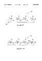
- FIG. 1is a top view of a semiconductor wafer at one processing step in accordance with the invention.
- FIG. 2is an enlarged sectional view of a portion of the FIG. 1 wafer at a processing step subsequent to that depicted by FIG. 1.
- FIG. 3is an enlarged sectional view of a portion of the FIG. 1 wafer at a processing step subsequent to that depicted by FIG. 2.
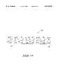
- FIG. 4is an enlarged sectional view of a portion of the FIG. 1 wafer at an alternate processing step subsequent to that depicted by FIG. 2 and corresponding in sequence to that of FIG. 3.
- FIG. 5is a view of the FIG. 3 wafer at a processing step subsequent to that depicted by FIG. 3.
- FIG. 6is a view of the FIG. 4 wafer at an alternate processing step corresponding in sequence to that of FIG. 5.
- FIG. 7is a view of the FIG. 3 wafer at a processing step subsequent to that depicted by FIG. 5.
- FIG. 8is a view of the FIG. 4 wafer at a processing step subsequent to that depicted by FIG. 6 corresponding in sequence to that of FIG. 7.
- FIG. 9is a sectional view of an alternate embodiment semiconductor wafer fragment processed in accordance with alternate aspects of the invention.
- FIG. 10is a view of the FIG. 9 wafer at a processing step subsequent to that depicted by FIG. 9.
- FIG. 11is a view of the FIG. 9 wafer at a processing step subsequent to that depicted by FIG. 10.
- FIG. 12is a view of the FIG. 9 wafer at a processing step subsequent to that depicted by FIG. 11.
- FIG. 13is a view of the FIG. 9 wafer at a processing step subsequent to that depicted by FIG. 12.
- FIG. 14is a sectional view of yet another alternate embodiment wafer fragment at another alternate processing step in accordance with the invention.
- FIG. 15is a view of the FIG. 14 wafer at a processing step subsequent to that shown by FIG. 14.
- FIGS. 1 and 2illustrate a semiconductor wafer 10 in process.
- a circular metal carrier or process ring 12has an adhesive cutting film 14 stretched thereacross and adhered to the underside thereof.
- Adhesive film 14has an adhesive side 13 which faces the reader and a non-adhesive side 15 on the opposite side thereof.
- An example tape or cutting filmis Nitto Denko High Tack Tape V-8-5.
- Wafer 10is centrally positioned or located onto tape or film 14 for cutting.
- FIG. 1illustrates but one embodiment of how a wafer 10 can be configured for singulation into individual die.
- Wafer 10has been fabricated into discrete die areas 20 having integrated circuitry fabricated therewithin. Such inherently forms or defines street area or scribe lines 22 where circuitry has typically not been formed and where cutting will occur to achieve singulation into individual die.
- Wafer 10typically comprises an outermost passivation layer defining an outer insulating surface 24. Bond pads 26 are exposed through the passivation layer for making electrical connection between the resultant chip and circuitry or components external of the chip. Accordingly, bond pads 26 are formed within die areas 20 and are proximately associated with wafer outer surface 24. Bond pads 26 typically are received inwardly 0.8 micron from outer surface 24.
- bond pads 26have conductive material 28 in the form of bumps formed thereover by any conventional bumping or other technique.
- An exemplary projection distance of the outermost portion of bumps 28 from surface 24is from 4 to 6 mils.
- FIGS. 3, 5 and 7constitute but one processing sequence
- FIGS. 4, 6, and 8constitute an alternate processing sequence.
- Like numerals in the component numbering of the two seriesare utilized, with the suffix "a" or different numerals being utilized in the second FIGS. 4, 6 and 8 series to designate differences.
- first cutting of wafer 10 on film 14is conducted through outer surface 24 about die areas 20 over scribe lines 22 and only partially into wafer 10 to form a series of die cuts 30.
- An exemplary depth for cuts 30is less than or equal to about 50% of the wafer thickness.
- An example method of cuttingis mechanical sawing, such as using a saw blade 36, to provide die cuts 30 to have common first cut widths 34 corresponding to the thickness of saw blade 36.
- An example thickness 34is 4 mils. Alternate techniques for forming cuts 30 could also be used, such as laser cutting or etching.
- FIG. 4illustrates one alternate processing wherein cuts 30a are formed entirely through wafer 10a, forming side edges 32a.
- insulating material 38is formed over at least a portion of edges 32/32a within cuts 30/30a.
- An example materialis polyimide. As shown, such insulating material covers all of cut edges 32/32a within cuts 30/30a, and insulating material 38 completely fills and overfills cuts 30/30a. The overfilling also forms insulating material 38 over portions of die area outer surfaces 24, such as the illustrated portions 39. Thus, insulating material 38 is adhered to at least a portion of side edges 32/32a yet is not formed over bond pads 26. Insulating material 38 is accordingly ideally continuous in extension over those portions of side edges 32/32a to which it adheres and portion 39 of outer surface 24 to which it adheres. An exemplary distance for insulative material 38 to project from outer surface 24 is 0.5 mil. This is also ideally less than the distance which bumps 28 project to avoid any interference in subsequent bonding of the discrete flip chips to other substrates.
- One method of forming or applying insulating material 38is by ejection from a syringe, such as the illustrated syringe 40, into the respective cuts to totally fill such cuts with insulating material. Alternate techniques could of course be utilized, with but one such technique being described subsequently. With the syringe or other preferred techniques, the insulating material layer forming occurs while wafer 10 is adhered to adhesive cutting film 14.
- Second cuts 42/42ahave different widths from the first cut widths, with the first cut widths preferably being at least three times as great as the second cut widths.
- an example techniqueis mechanical sawing using a second saw blade 37 of different thickness than the first saw blade, with an example being 1.2 mils. Accordingly in such embodiment, all of the cutting and forming of insulating material occurs while wafer 10 is adhered to a single adhesive cutting film 14.
- the second cuttingalso cuts through semiconductive material of wafer 10 through the bases of first cuts 30/30a.
- first cuts 30aextend entirely through wafer 10 and the second cut is to a second thinner width than first cut in between edges 32a
- such second cuttingdoes not cut through any semiconductive material of wafer 10.
- the second cutspreferably leave a thickness of insulating material 38 over cut edges 32/32a of between about 100 Angstroms and 100 microns. More preferably, such thickness is between about 10 microns and 100 microns, with 25 microns being a specific example. Accordingly, such insulating material 38 is provided to be adhered over only a portion of outer insulating surface 24 and adhered to at least a portion of side edges 32/32a, and preferably over all of such side edges.
- FIGS. 9-11Alternate exemplary processing is described with reference to FIGS. 9-11. Like numerals from the first described embodiments are utilized where appropriate, with the differences being indicated by the suffix "b", or with different numerals.
- a wafer 10bis adhered to an adhesive film carrier 14b for cutting. Wafer 10b and film 14b can be the same as that described with respect to the first embodiments. Cuts 50, preferably corresponding to those of cuts 30a of the first embodiments, are formed partially into wafer 10b. Such form cut side edges 52.
- wafer 10bis removed from adhesive film 14b.
- An insulative material 38bis then deposited over outer surface 24 of wafer 10b and to within cuts 50 to at least partially cover cut edges 52 and to only partially fill such cuts with insulative material.
- formation of an insulating material over at least a portion of the cut edgesoccurs while the wafer is not adhered to any adhesive cutting film.
- insulative material 38bis removed from being received over bond pads 26 while leaving insulative material within die cuts 50. Ideally as shown, the removing leaves some insulating material 38b over die area outer surfaces 24, such as portions of 39b as shown.
- a preferred method for producing the FIG. 11 removalis by photopatterning and etching. A polishing process might also be utilized, but would most likely not in such instance leave any insulating material remaining over die area outer surfaces 24.
- FIG. 11 waferhas been bumped with conductive material as in the first described embodiment for the exemplary ultimate forming of flip chips.
- wafer 10bis again adhered to another or same adhesive cutting film 14b. Thereafter, cutting is conducted into and through insulative material 38b within die cuts 50 and through wafer 10b.
- the preferred cutting methodsare to utilize two saws of different thicknesses, with the first cut being at least three times as wide as the second.
- FIGS. 14-15Yet another alternate embodiment is described with reference to FIGS. 14-15. Like numerals from the first described embodiments are utilized where appropriate, with differences being indicated by the suffix "c" or with different numerals.
- a wafer 10cis adhered to a stretchable adhesive cutting film 14c. Many cutting films, such as the Nitto Denko High Tack Tape V-8-5 example tape, are stretchable. Wafer 10c is subjected to cutting on film 14c into spaced individual die 60 having cuts 30c, with cut edges 32c, formed therebetween.
- the cuts to form 30ccan desirably be conducted with a thinner blade than that described with respect to the other embodiments, such as for example with a desired finish cutting thickness blade of 1.2 mils. Such will provide a first average spacing of cuts 30c which can be the same, or even less than, the final cut.
- adhesive film 14cis stretched to space the illustrated die further apart from one another to a second average spacing 62 which is greater than the spacing provided by cuts 30c.
- the second spacing relationship relative to the first spacing relationshipis analogous with that described with respect to the above embodiments. Namely, the spacing in FIG. 15 is preferably at least three times as great as the desired finish cut width.
- Second spaces 62would be at least partially filled with insulative material effective to cover at least some portion of cut die edges 32c.
- cuttingwould be conducted into and through such formed insulating material between adjacent die to form singulated die on film 14c. This final cutting could utilize a saw the same width as the saw used for the FIG. 14 cutting, or utilizing a saw of a different width.
Landscapes
- Engineering & Computer Science (AREA)
- Physics & Mathematics (AREA)
- Condensed Matter Physics & Semiconductors (AREA)
- General Physics & Mathematics (AREA)
- Computer Hardware Design (AREA)
- Microelectronics & Electronic Packaging (AREA)
- Power Engineering (AREA)
- Manufacturing & Machinery (AREA)
- Dicing (AREA)
Abstract
Description
Claims (31)
Priority Applications (1)
| Application Number | Priority Date | Filing Date | Title |
|---|---|---|---|
| US09/235,567US6074896A (en) | 1997-08-20 | 1999-01-22 | Method of processing semiconductor material wafers and method of forming flip chips and semiconductor chips |
Applications Claiming Priority (2)
| Application Number | Priority Date | Filing Date | Title |
|---|---|---|---|
| US08/917,004US5863813A (en) | 1997-08-20 | 1997-08-20 | Method of processing semiconductive material wafers and method of forming flip chips and semiconductor chips |
| US09/235,567US6074896A (en) | 1997-08-20 | 1999-01-22 | Method of processing semiconductor material wafers and method of forming flip chips and semiconductor chips |
Related Parent Applications (1)
| Application Number | Title | Priority Date | Filing Date |
|---|---|---|---|
| US08/917,004ContinuationUS5863813A (en) | 1997-08-20 | 1997-08-20 | Method of processing semiconductive material wafers and method of forming flip chips and semiconductor chips |
Publications (1)
| Publication Number | Publication Date |
|---|---|
| US6074896Atrue US6074896A (en) | 2000-06-13 |
Family
ID=25438218
Family Applications (3)
| Application Number | Title | Priority Date | Filing Date |
|---|---|---|---|
| US08/917,004Expired - LifetimeUS5863813A (en) | 1997-08-20 | 1997-08-20 | Method of processing semiconductive material wafers and method of forming flip chips and semiconductor chips |
| US09/035,777Expired - LifetimeUS6051875A (en) | 1997-08-20 | 1998-03-04 | Semiconductor chip |
| US09/235,567Expired - LifetimeUS6074896A (en) | 1997-08-20 | 1999-01-22 | Method of processing semiconductor material wafers and method of forming flip chips and semiconductor chips |
Family Applications Before (2)
| Application Number | Title | Priority Date | Filing Date |
|---|---|---|---|
| US08/917,004Expired - LifetimeUS5863813A (en) | 1997-08-20 | 1997-08-20 | Method of processing semiconductive material wafers and method of forming flip chips and semiconductor chips |
| US09/035,777Expired - LifetimeUS6051875A (en) | 1997-08-20 | 1998-03-04 | Semiconductor chip |
Country Status (1)
| Country | Link |
|---|---|
| US (3) | US5863813A (en) |
Cited By (33)
| Publication number | Priority date | Publication date | Assignee | Title |
|---|---|---|---|---|
| US6245595B1 (en)* | 1999-07-22 | 2001-06-12 | National Semiconductor Corporation | Techniques for wafer level molding of underfill encapsulant |
| US6268237B1 (en)* | 1995-04-03 | 2001-07-31 | Aptek Industries, Inc. | Stress-free silicon wafer and a die or chip made therefrom and method |
| US6281047B1 (en)* | 2000-11-10 | 2001-08-28 | Siliconware Precision Industries, Co., Ltd. | Method of singulating a batch of integrated circuit package units constructed on a single matrix base |
| US6287895B1 (en)* | 1999-01-29 | 2001-09-11 | Nec Corporation | Semiconductor package having enhanced ball grid array protective dummy members |
| US20030022465A1 (en)* | 2001-07-27 | 2003-01-30 | Wachtler Kurt P. | Method of separating semiconductor dies from a wafer |
| US20030052410A1 (en)* | 2001-09-18 | 2003-03-20 | Seiko Epson Corporation | Semiconductor wafer, semiconductor device and method of manufacturing the same, circuit board, and electronic device |
| US20030161069A1 (en)* | 2002-02-27 | 2003-08-28 | Seagate Technology, Llc | Wafer-level fabrication method for top or side slider bond pads |
| WO2003028949A3 (en)* | 2001-10-01 | 2004-04-01 | Xsil Technology Ltd | Method of machining substrates |
| US20040121563A1 (en)* | 2002-03-06 | 2004-06-24 | Farnworth Warren M. | Method for fabricating encapsulated semiconductor components having conductive vias |
| US6759311B2 (en)* | 2001-10-31 | 2004-07-06 | Formfactor, Inc. | Fan out of interconnect elements attached to semiconductor wafer |
| US6759276B1 (en) | 2002-07-30 | 2004-07-06 | Taiwan Semiconductor Manufacturing Company | Material to improve CMOS image sensor yield during wafer sawing |
| US20040180473A1 (en)* | 2003-03-11 | 2004-09-16 | Akihito Kawai | Method of dividing a semiconductor wafer |
| US20040238926A1 (en)* | 2003-03-20 | 2004-12-02 | Seiko Epson Corporation | Semiconductor wafer, semiconductor device and method for manufacturing same, circuit board, and electronic apparatus |
| US20050167799A1 (en)* | 2004-01-29 | 2005-08-04 | Doan Trung T. | Method of fabricating wafer-level packaging with sidewall passivation and related apparatus |
| US20050223543A1 (en)* | 2003-12-31 | 2005-10-13 | Microfabrica Inc. | Electrochemical fabrication method for fabricating space transformers or co-fabricating probes and space transformers |
| US20060046438A1 (en)* | 2004-08-31 | 2006-03-02 | Kirby Kyle K | Wafer reinforcement structure and methods of fabrication |
| US7071032B2 (en) | 2002-08-01 | 2006-07-04 | Taiwan Semiconductor Manufacturing Co., Ltd. | Material to improve image sensor yield during wafer sawing |
| US20060237850A1 (en)* | 2005-04-20 | 2006-10-26 | Yuan Yuan | Semiconductor die edge reconditioning |
| US20070029684A1 (en)* | 2005-08-02 | 2007-02-08 | Disco Corporation | Wafer dividing method |
| US20070148991A1 (en)* | 2005-12-23 | 2007-06-28 | Fei Company | Method of fabricating nanodevices |
| US20070224732A1 (en)* | 2006-03-24 | 2007-09-27 | Advanced Semiconductor Engineering, Inc. | Manufacturing method of a package structure |
| US20080124843A1 (en)* | 1999-12-27 | 2008-05-29 | Shinji Ohuchi | Resin for sealing semiconductor device, resin-sealed semiconductor device and the method of manufacturing the semiconductor device |
| US20080153265A1 (en)* | 2006-12-21 | 2008-06-26 | Texas Instruments Incorporated | Semiconductor Device Manufactured Using an Etch to Separate Wafer into Dies and Increase Device Space on a Wafer |
| US20080233711A1 (en)* | 2007-03-19 | 2008-09-25 | Disco Corporation | Manufacturing method for devices |
| US20080260841A1 (en)* | 2003-04-09 | 2008-10-23 | Leach Robert M | Micronized wood preservative formulations |
| US20090280584A1 (en)* | 2008-02-04 | 2009-11-12 | Micron Technology, Inc. | Wafer processing |
| US20110229822A1 (en)* | 2008-11-25 | 2011-09-22 | Stapleton Russell A | Methods for protecting a die surface with photocurable materials |
| US8778407B2 (en) | 2003-04-09 | 2014-07-15 | Osmose, Inc. | Micronized wood preservative formulations |
| US20150118797A1 (en)* | 2013-10-30 | 2015-04-30 | Taiwan Semiconductor Manufacturing Company, Ltd. | Method for Singulating Packaged Integrated Circuits and Resulting Structures |
| US9093448B2 (en) | 2008-11-25 | 2015-07-28 | Lord Corporation | Methods for protecting a die surface with photocurable materials |
| US10416192B2 (en) | 2003-02-04 | 2019-09-17 | Microfabrica Inc. | Cantilever microprobes for contacting electronic components |
| US11262383B1 (en) | 2018-09-26 | 2022-03-01 | Microfabrica Inc. | Probes having improved mechanical and/or electrical properties for making contact between electronic circuit elements and methods for making |
| US20230098907A1 (en)* | 2021-09-30 | 2023-03-30 | Texas Instruments Incorporated | Package geometries to enable visual inspection of solder fillets |
Families Citing this family (37)
| Publication number | Priority date | Publication date | Assignee | Title |
|---|---|---|---|---|
| US6077757A (en)* | 1997-05-15 | 2000-06-20 | Nec Corporation | Method of forming chip semiconductor devices |
| US5863813A (en)* | 1997-08-20 | 1999-01-26 | Micron Communications, Inc. | Method of processing semiconductive material wafers and method of forming flip chips and semiconductor chips |
| US6235551B1 (en) | 1997-12-31 | 2001-05-22 | Micron Technology, Inc. | Semiconductor device including edge bond pads and methods |
| US6207474B1 (en) | 1998-03-09 | 2001-03-27 | Micron Technology, Inc. | Method of forming a stack of packaged memory die and resulting apparatus |
| US6341070B1 (en)* | 1998-07-28 | 2002-01-22 | Ho-Yuan Yu | Wafer-scale packing processes for manufacturing integrated circuit (IC) packages |
| JP2000138262A (en) | 1998-10-31 | 2000-05-16 | Anam Semiconductor Inc | Chip-scale semiconductor package and method of manufacturing the same |
| JP3816253B2 (en)* | 1999-01-19 | 2006-08-30 | 富士通株式会社 | Manufacturing method of semiconductor device |
| US6182342B1 (en) | 1999-04-02 | 2001-02-06 | Andersen Laboratories, Inc. | Method of encapsulating a saw device |
| US6414396B1 (en) | 2000-01-24 | 2002-07-02 | Amkor Technology, Inc. | Package for stacked integrated circuits |
| JP3573048B2 (en)* | 2000-02-14 | 2004-10-06 | 松下電器産業株式会社 | Method for manufacturing semiconductor device |
| JP4403631B2 (en)* | 2000-04-24 | 2010-01-27 | ソニー株式会社 | Manufacturing method of chip-shaped electronic component and manufacturing method of pseudo wafer used for manufacturing the same |
| JP2001313350A (en)* | 2000-04-28 | 2001-11-09 | Sony Corp | Chip-shaped electronic component and its manufacturing method, and pseudo-wafer used for manufacture of chip- shaped electronic component and its manufacturing method |
| US6406934B1 (en)* | 2000-09-05 | 2002-06-18 | Amkor Technology, Inc. | Wafer level production of chip size semiconductor packages |
| JP4659300B2 (en)* | 2000-09-13 | 2011-03-30 | 浜松ホトニクス株式会社 | Laser processing method and semiconductor chip manufacturing method |
| DE10206661A1 (en)* | 2001-02-20 | 2002-09-26 | Infineon Technologies Ag | Electronic component used in semiconductors comprises a semiconductor chip surrounded by a sawn edge having profile-sawn contours of semiconductor material and surrounded by a plastic composition forming a plastic edge |
| JP2003100666A (en)* | 2001-09-26 | 2003-04-04 | Toshiba Corp | Method for manufacturing semiconductor device |
| DK200200178A (en)* | 2002-02-06 | 2003-08-07 | Vestas Wind Sys As | Wind turbine tower suspension means |
| JP2004221125A (en)* | 2003-01-09 | 2004-08-05 | Sharp Corp | Semiconductor device and manufacturing method thereof |
| US7510908B1 (en)* | 2003-02-20 | 2009-03-31 | National Semiconductor Corporation | Method to dispense light blocking material for wafer level CSP |
| WO2005078789A1 (en)* | 2004-01-13 | 2005-08-25 | Infineon Technologies Ag | Chip-sized filp-chip semiconductor package and method for making the same |
| US7129114B2 (en)* | 2004-03-10 | 2006-10-31 | Micron Technology, Inc. | Methods relating to singulating semiconductor wafers and wafer scale assemblies |
| US8062925B2 (en)* | 2006-05-16 | 2011-11-22 | Koninklijke Philips Electronics N.V. | Process for preparing a semiconductor light-emitting device for mounting |
| US7382143B2 (en)* | 2006-05-18 | 2008-06-03 | Centipede Systems, Inc. | Wafer probe interconnect system |
| US8026599B2 (en)* | 2006-09-07 | 2011-09-27 | Analog Devices, Inc. | Method of protecting integrated circuits |
| US8859396B2 (en) | 2007-08-07 | 2014-10-14 | Semiconductor Components Industries, Llc | Semiconductor die singulation method |
| US7781310B2 (en) | 2007-08-07 | 2010-08-24 | Semiconductor Components Industries, Llc | Semiconductor die singulation method |
| US7442045B1 (en)* | 2007-08-17 | 2008-10-28 | Centipede Systems, Inc. | Miniature electrical ball and tube socket with self-capturing multiple-contact-point coupling |
| JP5625558B2 (en)* | 2010-02-22 | 2014-11-19 | サンケン電気株式会社 | Semiconductor wafer and method for manufacturing semiconductor device |
| JP2014007228A (en)* | 2012-06-22 | 2014-01-16 | Ps4 Luxco S A R L | Semiconductor device and manufacturing method of the same |
| US9484260B2 (en) | 2012-11-07 | 2016-11-01 | Semiconductor Components Industries, Llc | Heated carrier substrate semiconductor die singulation method |
| US9136173B2 (en) | 2012-11-07 | 2015-09-15 | Semiconductor Components Industries, Llc | Singulation method for semiconductor die having a layer of material along one major surface |
| US9418894B2 (en) | 2014-03-21 | 2016-08-16 | Semiconductor Components Industries, Llc | Electronic die singulation method |
| US9385041B2 (en) | 2014-08-26 | 2016-07-05 | Semiconductor Components Industries, Llc | Method for insulating singulated electronic die |
| CN106558539A (en)* | 2015-09-25 | 2017-04-05 | 上海先进半导体制造股份有限公司 | The scribing of chip and manufacture method |
| US10366923B2 (en) | 2016-06-02 | 2019-07-30 | Semiconductor Components Industries, Llc | Method of separating electronic devices having a back layer and apparatus |
| US10373869B2 (en) | 2017-05-24 | 2019-08-06 | Semiconductor Components Industries, Llc | Method of separating a back layer on a substrate using exposure to reduced temperature and related apparatus |
| US10818551B2 (en) | 2019-01-09 | 2020-10-27 | Semiconductor Components Industries, Llc | Plasma die singulation systems and related methods |
Citations (11)
| Publication number | Priority date | Publication date | Assignee | Title |
|---|---|---|---|---|
| US4075632A (en)* | 1974-08-27 | 1978-02-21 | The United States Of America As Represented By The United States Department Of Energy | Interrogation, and detection system |
| US4926182A (en)* | 1986-05-30 | 1990-05-15 | Sharp Kabushiki Kaisha | Microwave data transmission apparatus |
| US5169804A (en)* | 1990-09-06 | 1992-12-08 | Siemens Aktiengesellschaft | Method for fastening a semiconductor, body provided with at least one semiconductor component to a substrate |
| US5391915A (en)* | 1978-11-20 | 1995-02-21 | Hatachi, Ltd. | Integrated circuit having reduced soft errors and reduced penetration of alkali impurities into the substrate |
| US5455455A (en)* | 1992-09-14 | 1995-10-03 | Badehi; Peirre | Methods for producing packaged integrated circuit devices and packaged integrated circuit devices produced thereby |
| US5501104A (en)* | 1993-02-23 | 1996-03-26 | Tokyo Seimitsu Co., Ltd. | Method of measuring the depth of full-cut dicing grooves by using an ultrasonic detector and a dicing apparatus for carrying out the same |
| US5583370A (en)* | 1994-03-04 | 1996-12-10 | Motorola Inc. | Tab semiconductor device having die edge protection and method for making the same |
| US5621412A (en)* | 1994-04-26 | 1997-04-15 | Texas Instruments Incorporated | Multi-stage transponder wake-up, method and structure |
| US5649296A (en)* | 1995-06-19 | 1997-07-15 | Lucent Technologies Inc. | Full duplex modulated backscatter system |
| US5863813A (en)* | 1997-08-20 | 1999-01-26 | Micron Communications, Inc. | Method of processing semiconductive material wafers and method of forming flip chips and semiconductor chips |
| US5903044A (en)* | 1996-03-12 | 1999-05-11 | Micron Technology, Inc. | Hermetic chip and method of manufacture |
- 1997
- 1997-08-20USUS08/917,004patent/US5863813A/ennot_activeExpired - Lifetime
- 1998
- 1998-03-04USUS09/035,777patent/US6051875A/ennot_activeExpired - Lifetime
- 1999
- 1999-01-22USUS09/235,567patent/US6074896A/ennot_activeExpired - Lifetime
Patent Citations (11)
| Publication number | Priority date | Publication date | Assignee | Title |
|---|---|---|---|---|
| US4075632A (en)* | 1974-08-27 | 1978-02-21 | The United States Of America As Represented By The United States Department Of Energy | Interrogation, and detection system |
| US5391915A (en)* | 1978-11-20 | 1995-02-21 | Hatachi, Ltd. | Integrated circuit having reduced soft errors and reduced penetration of alkali impurities into the substrate |
| US4926182A (en)* | 1986-05-30 | 1990-05-15 | Sharp Kabushiki Kaisha | Microwave data transmission apparatus |
| US5169804A (en)* | 1990-09-06 | 1992-12-08 | Siemens Aktiengesellschaft | Method for fastening a semiconductor, body provided with at least one semiconductor component to a substrate |
| US5455455A (en)* | 1992-09-14 | 1995-10-03 | Badehi; Peirre | Methods for producing packaged integrated circuit devices and packaged integrated circuit devices produced thereby |
| US5501104A (en)* | 1993-02-23 | 1996-03-26 | Tokyo Seimitsu Co., Ltd. | Method of measuring the depth of full-cut dicing grooves by using an ultrasonic detector and a dicing apparatus for carrying out the same |
| US5583370A (en)* | 1994-03-04 | 1996-12-10 | Motorola Inc. | Tab semiconductor device having die edge protection and method for making the same |
| US5621412A (en)* | 1994-04-26 | 1997-04-15 | Texas Instruments Incorporated | Multi-stage transponder wake-up, method and structure |
| US5649296A (en)* | 1995-06-19 | 1997-07-15 | Lucent Technologies Inc. | Full duplex modulated backscatter system |
| US5903044A (en)* | 1996-03-12 | 1999-05-11 | Micron Technology, Inc. | Hermetic chip and method of manufacture |
| US5863813A (en)* | 1997-08-20 | 1999-01-26 | Micron Communications, Inc. | Method of processing semiconductive material wafers and method of forming flip chips and semiconductor chips |
Cited By (77)
| Publication number | Priority date | Publication date | Assignee | Title |
|---|---|---|---|---|
| US6268237B1 (en)* | 1995-04-03 | 2001-07-31 | Aptek Industries, Inc. | Stress-free silicon wafer and a die or chip made therefrom and method |
| US6576990B2 (en) | 1995-04-03 | 2003-06-10 | Aptek Industries, Inc. | Stress-free silicon wafer and a die or chip made therefrom and method |
| US6287895B1 (en)* | 1999-01-29 | 2001-09-11 | Nec Corporation | Semiconductor package having enhanced ball grid array protective dummy members |
| US6245595B1 (en)* | 1999-07-22 | 2001-06-12 | National Semiconductor Corporation | Techniques for wafer level molding of underfill encapsulant |
| US20080124843A1 (en)* | 1999-12-27 | 2008-05-29 | Shinji Ohuchi | Resin for sealing semiconductor device, resin-sealed semiconductor device and the method of manufacturing the semiconductor device |
| US7704801B2 (en) | 1999-12-27 | 2010-04-27 | Oki Semiconductor Co., Ltd. | Resin for sealing semiconductor device, resin-sealed semiconductor device and the method of manufacturing the semiconductor device |
| US6281047B1 (en)* | 2000-11-10 | 2001-08-28 | Siliconware Precision Industries, Co., Ltd. | Method of singulating a batch of integrated circuit package units constructed on a single matrix base |
| US6686225B2 (en)* | 2001-07-27 | 2004-02-03 | Texas Instruments Incorporated | Method of separating semiconductor dies from a wafer |
| US20030022465A1 (en)* | 2001-07-27 | 2003-01-30 | Wachtler Kurt P. | Method of separating semiconductor dies from a wafer |
| US6734554B2 (en)* | 2001-09-18 | 2004-05-11 | Seiko Epson Corporation | Semiconductor wafer with bumps of uniform height |
| US20030052410A1 (en)* | 2001-09-18 | 2003-03-20 | Seiko Epson Corporation | Semiconductor wafer, semiconductor device and method of manufacturing the same, circuit board, and electronic device |
| US8048774B2 (en) | 2001-10-01 | 2011-11-01 | Electro Scientific Industries, Inc. | Methods and systems for laser machining a substrate |
| WO2003028949A3 (en)* | 2001-10-01 | 2004-04-01 | Xsil Technology Ltd | Method of machining substrates |
| US6759311B2 (en)* | 2001-10-31 | 2004-07-06 | Formfactor, Inc. | Fan out of interconnect elements attached to semiconductor wafer |
| US20030161069A1 (en)* | 2002-02-27 | 2003-08-28 | Seagate Technology, Llc | Wafer-level fabrication method for top or side slider bond pads |
| US7254885B2 (en)* | 2002-02-27 | 2007-08-14 | Seagate Technology, Llc | Wafer-level fabrication method for top or side slider bond pads |
| US7157353B2 (en) | 2002-03-06 | 2007-01-02 | Micron Technology, Inc. | Method for fabricating encapsulated semiconductor components |
| US7776647B2 (en) | 2002-03-06 | 2010-08-17 | Micron Technology, Inc. | Semiconductor components and methods of fabrication with circuit side contacts, conductive vias and backside conductors |
| US7382060B2 (en) | 2002-03-06 | 2008-06-03 | Micron Technology, Inc. | Semiconductor component having thinned die, polymer layers, contacts on opposing sides, and conductive vias connecting the contacts |
| US20050181540A1 (en)* | 2002-03-06 | 2005-08-18 | Farnworth Warren M. | Semiconductor component and system having thinned, encapsulated dice |
| US20050200028A1 (en)* | 2002-03-06 | 2005-09-15 | Farnworth Warren M. | Encapsulated semiconductor component having thinned die with conductive vias |
| US20050227415A1 (en)* | 2002-03-06 | 2005-10-13 | Farnworth Warren M | Method for fabricating encapsulated semiconductor components |
| US20040121563A1 (en)* | 2002-03-06 | 2004-06-24 | Farnworth Warren M. | Method for fabricating encapsulated semiconductor components having conductive vias |
| US6964915B2 (en) | 2002-03-06 | 2005-11-15 | Micron Technology, Inc. | Method of fabricating encapsulated semiconductor components by etching |
| US20050269700A1 (en)* | 2002-03-06 | 2005-12-08 | Farnworth Warren M | Semiconductor component and system having thinned, encapsulated dice |
| US7432604B2 (en) | 2002-03-06 | 2008-10-07 | Micron Technology, Inc. | Semiconductor component and system having thinned, encapsulated dice |
| US7029949B2 (en) | 2002-03-06 | 2006-04-18 | Micron Technology, Inc. | Method for fabricating encapsulated semiconductor components having conductive vias |
| US20060118953A1 (en)* | 2002-03-06 | 2006-06-08 | Farnworth Warren M | Semiconductor component having thinned die with conductive vias |
| US7482702B2 (en) | 2002-03-06 | 2009-01-27 | Micron Technology, Inc. | Semiconductor component sealed on five sides by polymer sealing layer |
| US20060183349A1 (en)* | 2002-03-06 | 2006-08-17 | Farnworth Warren M | Semiconductor component having thinned die with polymer layers |
| US6908784B1 (en) | 2002-03-06 | 2005-06-21 | Micron Technology, Inc. | Method for fabricating encapsulated semiconductor components |
| US20050148160A1 (en)* | 2002-03-06 | 2005-07-07 | Farnworth Warren M. | Encapsulated semiconductor components and methods of fabrication |
| US7221059B2 (en) | 2002-03-06 | 2007-05-22 | Micron Technology, Inc. | Wafer level semiconductor component having thinned, encapsulated dice and polymer dam |
| US7417325B2 (en) | 2002-03-06 | 2008-08-26 | Micron Technology, Inc. | Semiconductor component having thinned die with conductive vias configured as conductive pin terminal contacts |
| US6759276B1 (en) | 2002-07-30 | 2004-07-06 | Taiwan Semiconductor Manufacturing Company | Material to improve CMOS image sensor yield during wafer sawing |
| US7071032B2 (en) | 2002-08-01 | 2006-07-04 | Taiwan Semiconductor Manufacturing Co., Ltd. | Material to improve image sensor yield during wafer sawing |
| US10416192B2 (en) | 2003-02-04 | 2019-09-17 | Microfabrica Inc. | Cantilever microprobes for contacting electronic components |
| US10788512B2 (en) | 2003-02-04 | 2020-09-29 | Microfabrica Inc. | Cantilever microprobes for contacting electronic components |
| US20040180473A1 (en)* | 2003-03-11 | 2004-09-16 | Akihito Kawai | Method of dividing a semiconductor wafer |
| US7129150B2 (en)* | 2003-03-11 | 2006-10-31 | Disco Corporation | Method of dividing a semiconductor wafer |
| US20040238926A1 (en)* | 2003-03-20 | 2004-12-02 | Seiko Epson Corporation | Semiconductor wafer, semiconductor device and method for manufacturing same, circuit board, and electronic apparatus |
| US20090092683A1 (en)* | 2003-04-09 | 2009-04-09 | Leach Robert M | Micronized Wood Preservative Formulations |
| US20090035564A1 (en)* | 2003-04-09 | 2009-02-05 | Leach Robert M | Micronized Wood Preservative Formulations |
| US20080260841A1 (en)* | 2003-04-09 | 2008-10-23 | Leach Robert M | Micronized wood preservative formulations |
| US8778407B2 (en) | 2003-04-09 | 2014-07-15 | Osmose, Inc. | Micronized wood preservative formulations |
| US7640651B2 (en)* | 2003-12-31 | 2010-01-05 | Microfabrica Inc. | Fabrication process for co-fabricating multilayer probe array and a space transformer |
| US20050223543A1 (en)* | 2003-12-31 | 2005-10-13 | Microfabrica Inc. | Electrochemical fabrication method for fabricating space transformers or co-fabricating probes and space transformers |
| US7656012B2 (en) | 2004-01-29 | 2010-02-02 | Micron Technology, Inc. | Apparatus for use in semiconductor wafer processing for laterally displacing individual semiconductor devices away from one another |
| US20050167799A1 (en)* | 2004-01-29 | 2005-08-04 | Doan Trung T. | Method of fabricating wafer-level packaging with sidewall passivation and related apparatus |
| US20060197190A1 (en)* | 2004-01-29 | 2006-09-07 | Doan Trung T | Method of fabricating wafer-level packaging with sidewall passivation and related apparatus |
| US20100102433A1 (en)* | 2004-01-29 | 2010-04-29 | Micron Technology, Inc. | Apparatus for use in semiconductor wafer processing for laterally displacing individual semiconductor devices away from one another |
| US7169691B2 (en)* | 2004-01-29 | 2007-01-30 | Micron Technology, Inc. | Method of fabricating wafer-level packaging with sidewall passivation and related apparatus |
| US7332413B2 (en) | 2004-08-31 | 2008-02-19 | Micron Tecnology, Inc. | Semiconductor wafers including one or more reinforcement structures and methods of forming the same |
| US20060046438A1 (en)* | 2004-08-31 | 2006-03-02 | Kirby Kyle K | Wafer reinforcement structure and methods of fabrication |
| US7244663B2 (en) | 2004-08-31 | 2007-07-17 | Micron Technology, Inc. | Wafer reinforcement structure and methods of fabrication |
| US7374971B2 (en)* | 2005-04-20 | 2008-05-20 | Freescale Semiconductor, Inc. | Semiconductor die edge reconditioning |
| US20060237850A1 (en)* | 2005-04-20 | 2006-10-26 | Yuan Yuan | Semiconductor die edge reconditioning |
| US7727810B2 (en)* | 2005-08-02 | 2010-06-01 | Disco Corporation | Wafer dividing method |
| US20070029684A1 (en)* | 2005-08-02 | 2007-02-08 | Disco Corporation | Wafer dividing method |
| US7544523B2 (en)* | 2005-12-23 | 2009-06-09 | Fei Company | Method of fabricating nanodevices |
| US20070148991A1 (en)* | 2005-12-23 | 2007-06-28 | Fei Company | Method of fabricating nanodevices |
| US7442580B2 (en)* | 2006-03-24 | 2008-10-28 | Advanced Semiconductor Engineering, Inc. | Manufacturing method of a package structure |
| US20070224732A1 (en)* | 2006-03-24 | 2007-09-27 | Advanced Semiconductor Engineering, Inc. | Manufacturing method of a package structure |
| US20080153265A1 (en)* | 2006-12-21 | 2008-06-26 | Texas Instruments Incorporated | Semiconductor Device Manufactured Using an Etch to Separate Wafer into Dies and Increase Device Space on a Wafer |
| US7825009B2 (en)* | 2007-03-19 | 2010-11-02 | Disco Corporation | Manufacturing method for devices |
| US20080233711A1 (en)* | 2007-03-19 | 2008-09-25 | Disco Corporation | Manufacturing method for devices |
| US20090280584A1 (en)* | 2008-02-04 | 2009-11-12 | Micron Technology, Inc. | Wafer processing |
| US7897485B2 (en)* | 2008-02-04 | 2011-03-01 | Micron Technology, Inc. | Wafer processing including forming trench rows and columns at least one of which has a different width |
| US8568961B2 (en) | 2008-11-25 | 2013-10-29 | Lord Corporation | Methods for protecting a die surface with photocurable materials |
| US9093448B2 (en) | 2008-11-25 | 2015-07-28 | Lord Corporation | Methods for protecting a die surface with photocurable materials |
| US20110229822A1 (en)* | 2008-11-25 | 2011-09-22 | Stapleton Russell A | Methods for protecting a die surface with photocurable materials |
| US9875913B2 (en)* | 2013-10-30 | 2018-01-23 | Taiwan Semiconductor Manufacturing Company, Ltd. | Method for singulating packaged integrated circuits and resulting structures |
| US20150118797A1 (en)* | 2013-10-30 | 2015-04-30 | Taiwan Semiconductor Manufacturing Company, Ltd. | Method for Singulating Packaged Integrated Circuits and Resulting Structures |
| US11262383B1 (en) | 2018-09-26 | 2022-03-01 | Microfabrica Inc. | Probes having improved mechanical and/or electrical properties for making contact between electronic circuit elements and methods for making |
| US11982689B2 (en) | 2018-09-26 | 2024-05-14 | Microfabrica Inc. | Probes having improved mechanical and/or electrical properties for making contact between electronic circuit elements and methods for making |
| US20230098907A1 (en)* | 2021-09-30 | 2023-03-30 | Texas Instruments Incorporated | Package geometries to enable visual inspection of solder fillets |
| US12354918B2 (en)* | 2021-09-30 | 2025-07-08 | Texas Instruments Incorporated | Package geometries to enable visual inspection of solder fillets |
Also Published As
| Publication number | Publication date |
|---|---|
| US5863813A (en) | 1999-01-26 |
| US6051875A (en) | 2000-04-18 |
Similar Documents
| Publication | Publication Date | Title |
|---|---|---|
| US6074896A (en) | Method of processing semiconductor material wafers and method of forming flip chips and semiconductor chips | |
| JP3455762B2 (en) | Semiconductor device and manufacturing method thereof | |
| JP4109823B2 (en) | Manufacturing method of semiconductor device | |
| JP4856328B2 (en) | Manufacturing method of semiconductor device | |
| US6175162B1 (en) | Semiconductor wafer having a bottom surface protective coating | |
| US7064010B2 (en) | Methods of coating and singulating wafers | |
| US6649445B1 (en) | Wafer coating and singulation method | |
| US6083811A (en) | Method for producing thin dice from fragile materials | |
| EP0182218B1 (en) | Method for dicing semiconductor wafer | |
| JP2921953B2 (en) | Method for manufacturing semiconductor device | |
| US20020037631A1 (en) | Method for manufacturing semiconductor devices | |
| US20170092540A1 (en) | Plasma dicing with blade saw patterned underside mask | |
| US20100200986A1 (en) | Grooving Bumped Wafer Pre-Underfill System | |
| US20030102526A1 (en) | Backside metallization on sides of microelectronic dice for effective thermal contact with heat dissipation devices | |
| WO2013019499A2 (en) | Dicing before grinding after coating | |
| US20030143818A1 (en) | Method of applying a bottom surface protective coating to a wafer, and wafer dicing method | |
| US5316853A (en) | Expand tape | |
| US5762744A (en) | Method of producing a semiconductor device using an expand tape | |
| JP2000182995A (en) | Manufacture of semiconductor device | |
| JP2002043356A (en) | Semiconductor wafer, semiconductor device and manufacturing method therefor | |
| US7498236B2 (en) | Silicon wafer thinning end point method | |
| JP2001060591A (en) | Manufacture of semiconductor device | |
| US6264535B1 (en) | Wafer sawing/grinding process | |
| JP3803214B2 (en) | Manufacturing method of semiconductor device | |
| JPH03101128A (en) | Manufacture of semiconductor chip |
Legal Events
| Date | Code | Title | Description |
|---|---|---|---|
| AS | Assignment | Owner name:MICRON TECHNOLOGY, INC., IDAHO Free format text:MERGER;ASSIGNOR:MICRON COMMUNICATIONS, INC.;REEL/FRAME:010384/0086 Effective date:19990901 | |
| STCF | Information on status: patent grant | Free format text:PATENTED CASE | |
| FEPP | Fee payment procedure | Free format text:PAYOR NUMBER ASSIGNED (ORIGINAL EVENT CODE: ASPN); ENTITY STATUS OF PATENT OWNER: LARGE ENTITY | |
| CC | Certificate of correction | ||
| FPAY | Fee payment | Year of fee payment:4 | |
| AS | Assignment | Owner name:KEYSTONE TECHNOLOGY SOLUTIONS, LLC, IDAHO Free format text:ASSIGNMENT OF ASSIGNORS INTEREST;ASSIGNOR:MICRON TECHNOLOGY, INC.;REEL/FRAME:019825/0542 Effective date:20070628 Owner name:KEYSTONE TECHNOLOGY SOLUTIONS, LLC,IDAHO Free format text:ASSIGNMENT OF ASSIGNORS INTEREST;ASSIGNOR:MICRON TECHNOLOGY, INC.;REEL/FRAME:019825/0542 Effective date:20070628 | |
| FPAY | Fee payment | Year of fee payment:8 | |
| AS | Assignment | Owner name:ROUND ROCK RESEARCH, LLC,NEW YORK Free format text:ASSIGNMENT OF ASSIGNORS INTEREST;ASSIGNOR:MICRON TECHNOLOGY, INC.;REEL/FRAME:023786/0416 Effective date:20091223 Owner name:ROUND ROCK RESEARCH, LLC, NEW YORK Free format text:ASSIGNMENT OF ASSIGNORS INTEREST;ASSIGNOR:MICRON TECHNOLOGY, INC.;REEL/FRAME:023786/0416 Effective date:20091223 | |
| AS | Assignment | Owner name:MICRON TECHNOLOGY, INC., IDAHO Free format text:ASSIGNMENT OF ASSIGNORS INTEREST;ASSIGNOR:KEYSTONE TECHNOLOGY SOLUTIONS, LLC;REEL/FRAME:023839/0881 Effective date:20091222 Owner name:MICRON TECHNOLOGY, INC.,IDAHO Free format text:ASSIGNMENT OF ASSIGNORS INTEREST;ASSIGNOR:KEYSTONE TECHNOLOGY SOLUTIONS, LLC;REEL/FRAME:023839/0881 Effective date:20091222 | |
| FPAY | Fee payment | Year of fee payment:12 |