US6074103A - Aligning an optical fiber with electroluminescent semiconductor diodes and other optical components - Google Patents
Aligning an optical fiber with electroluminescent semiconductor diodes and other optical componentsDownload PDFInfo
- Publication number
- US6074103A US6074103AUS08/950,716US95071697AUS6074103AUS 6074103 AUS6074103 AUS 6074103AUS 95071697 AUS95071697 AUS 95071697AUS 6074103 AUS6074103 AUS 6074103A
- Authority
- US
- United States
- Prior art keywords
- optical fiber
- support member
- optical
- support
- carrier
- Prior art date
- Legal status (The legal status is an assumption and is not a legal conclusion. Google has not performed a legal analysis and makes no representation as to the accuracy of the status listed.)
- Expired - Fee Related
Links
- 239000013307optical fiberSubstances0.000titleclaimsabstractdescription157
- 230000003287optical effectEffects0.000titleclaimsabstractdescription84
- 239000004065semiconductorSubstances0.000titledescription6
- 238000000034methodMethods0.000claimsabstractdescription43
- 229910000679solderInorganic materials0.000claimsdescription32
- 239000000835fiberSubstances0.000claimsdescription16
- 238000005476solderingMethods0.000claimsdescription7
- 239000000463materialSubstances0.000description11
- 239000000758substrateSubstances0.000description6
- 239000013013elastic materialSubstances0.000description5
- 238000003780insertionMethods0.000description5
- 230000037431insertionEffects0.000description5
- 239000011347resinSubstances0.000description5
- 229920005989resinPolymers0.000description5
- 238000002844meltingMethods0.000description4
- 230000008018meltingEffects0.000description4
- XUIMIQQOPSSXEZ-UHFFFAOYSA-NSiliconChemical compound[Si]XUIMIQQOPSSXEZ-UHFFFAOYSA-N0.000description3
- 230000015572biosynthetic processEffects0.000description3
- 239000000919ceramicSubstances0.000description3
- 238000010438heat treatmentMethods0.000description3
- 238000004519manufacturing processMethods0.000description3
- 230000008569processEffects0.000description3
- 229910052710siliconInorganic materials0.000description3
- 239000010703siliconSubstances0.000description3
- 238000005323electroformingMethods0.000description2
- 239000002184metalSubstances0.000description2
- 229910052751metalInorganic materials0.000description2
- 239000000203mixtureSubstances0.000description2
- 230000005855radiationEffects0.000description2
- 239000004952PolyamideSubstances0.000description1
- 230000003466anti-cipated effectEffects0.000description1
- 230000004888barrier functionEffects0.000description1
- 239000000969carrierSubstances0.000description1
- 230000008859changeEffects0.000description1
- 239000011248coating agentSubstances0.000description1
- 238000000576coating methodMethods0.000description1
- 238000010276constructionMethods0.000description1
- 238000001816coolingMethods0.000description1
- 230000007123defenseEffects0.000description1
- 238000005553drillingMethods0.000description1
- 238000001312dry etchingMethods0.000description1
- 230000008030eliminationEffects0.000description1
- 238000003379elimination reactionMethods0.000description1
- 239000011888foilSubstances0.000description1
- 208000016339iris patternDiseases0.000description1
- 238000001465metallisationMethods0.000description1
- 150000002739metalsChemical class0.000description1
- 229920002647polyamidePolymers0.000description1
- 230000001681protective effectEffects0.000description1
- 230000009467reductionEffects0.000description1
- 238000004544sputter depositionMethods0.000description1
- 238000003631wet chemical etchingMethods0.000description1
Images


Classifications
- G—PHYSICS
- G02—OPTICS
- G02B—OPTICAL ELEMENTS, SYSTEMS OR APPARATUS
- G02B6/00—Light guides; Structural details of arrangements comprising light guides and other optical elements, e.g. couplings
- G02B6/24—Coupling light guides
- G02B6/42—Coupling light guides with opto-electronic elements
- G02B6/4201—Packages, e.g. shape, construction, internal or external details
- G02B6/4219—Mechanical fixtures for holding or positioning the elements relative to each other in the couplings; Alignment methods for the elements, e.g. measuring or observing methods especially used therefor
- G02B6/4236—Fixing or mounting methods of the aligned elements
- G—PHYSICS
- G02—OPTICS
- G02B—OPTICAL ELEMENTS, SYSTEMS OR APPARATUS
- G02B6/00—Light guides; Structural details of arrangements comprising light guides and other optical elements, e.g. couplings
- G02B6/24—Coupling light guides
- G02B6/42—Coupling light guides with opto-electronic elements
- G02B6/4201—Packages, e.g. shape, construction, internal or external details
- G02B6/4219—Mechanical fixtures for holding or positioning the elements relative to each other in the couplings; Alignment methods for the elements, e.g. measuring or observing methods especially used therefor
- G02B6/422—Active alignment, i.e. moving the elements in response to the detected degree of coupling or position of the elements
- G02B6/4225—Active alignment, i.e. moving the elements in response to the detected degree of coupling or position of the elements by a direct measurement of the degree of coupling, e.g. the amount of light power coupled to the fibre or the opto-electronic element
- G—PHYSICS
- G02—OPTICS
- G02B—OPTICAL ELEMENTS, SYSTEMS OR APPARATUS
- G02B6/00—Light guides; Structural details of arrangements comprising light guides and other optical elements, e.g. couplings
- G02B6/24—Coupling light guides
- G02B6/42—Coupling light guides with opto-electronic elements
- G02B6/4201—Packages, e.g. shape, construction, internal or external details
- G02B6/4219—Mechanical fixtures for holding or positioning the elements relative to each other in the couplings; Alignment methods for the elements, e.g. measuring or observing methods especially used therefor
- G02B6/422—Active alignment, i.e. moving the elements in response to the detected degree of coupling or position of the elements
- G02B6/4226—Positioning means for moving the elements into alignment, e.g. alignment screws, deformation of the mount
- G—PHYSICS
- G02—OPTICS
- G02B—OPTICAL ELEMENTS, SYSTEMS OR APPARATUS
- G02B6/00—Light guides; Structural details of arrangements comprising light guides and other optical elements, e.g. couplings
- G02B6/24—Coupling light guides
- G02B6/36—Mechanical coupling means
- G02B6/3628—Mechanical coupling means for mounting fibres to supporting carriers
- G02B6/3632—Mechanical coupling means for mounting fibres to supporting carriers characterised by the cross-sectional shape of the mechanical coupling means
- G02B6/3644—Mechanical coupling means for mounting fibres to supporting carriers characterised by the cross-sectional shape of the mechanical coupling means the coupling means being through-holes or wall apertures
- G—PHYSICS
- G02—OPTICS
- G02B—OPTICAL ELEMENTS, SYSTEMS OR APPARATUS
- G02B6/00—Light guides; Structural details of arrangements comprising light guides and other optical elements, e.g. couplings
- G02B6/24—Coupling light guides
- G02B6/42—Coupling light guides with opto-electronic elements
- G02B6/4201—Packages, e.g. shape, construction, internal or external details
- G02B6/4219—Mechanical fixtures for holding or positioning the elements relative to each other in the couplings; Alignment methods for the elements, e.g. measuring or observing methods especially used therefor
- G02B6/4236—Fixing or mounting methods of the aligned elements
- G02B6/4238—Soldering
Definitions
- the present inventionrelates generally to optical components including optical fibers.
- the present inventionrelates to aligning optical fibers with other optical components such as electroluminescent semiconductor diodes, photosensitive transducers and optical waveguides.
- Advantages offered by the present inventioninclude alignment and fixation of optical fiber at temperatures that permit optical component to operate safely, elimination or at least great reduction in the alignment shift of optical fiber as its position is fixed, and the ability to make fine adjustments in optical fiber alignment.
- a method for aligning an optical fiber with an optical component mounted on a basecomprises establishing a first position of support close to the optical component to achieve a substantially optimum alignment, and then establishing a second position of support farther from the optical component to refine the alignment.
- a method for aligning an optical fiber with an optical component mounted on a basecomprises passing the optical fiber through an opening of a support member mounted on the base, moving the optical fiber within the extent of the opening to achieve a substantially optimum alignment of a first end of the optical fiber with the optical component, and then fixing the optical fiber to the support member.
- a method for aligning an optical fiber with an optical component mounted on a basecomprises moving the optical fiber to achieve a substantially optimum alignment of a first end of the optical fiber with the optical component, and fixing the position of support in a manner that any shift in the position occurs in a direction that is substantially collinear with the optical axis of the optical fiber.
- a devicecomprises a base carrying an optical component and a support member, and an optical fiber supported by the support member such that a first end of the optical fiber is held in proximity to and in alignment with the optical component, and the support member grips the optical fiber within an interval along the optical fiber less than or equal to about one-third the diameter of the fiber.
- a devicecomprises a base carrying an optical component, a first support member and a second support member, and an optical fiber pivotally supported at the first support member and supported at the second support member such that a first end of the optical fiber is held in proximity to and in alignment with the optical component.
- a devicecomprises a base carrying an optical component and a support member, and an optical fiber supported by the support member such that a first end of the optical fiber is held in proximity to and in alignment with the optical component, and the optical fiber is attached to a carrier bonded to a surface of the support member that is substantially orthogonal to the optical axis of the optical fiber.
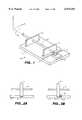
- FIG. 1is a schematic representation of one embodiment of a device according to the present invention.
- FIGS. 2a and 2bare schematic representations of two ways in which a support member may be mounted to a base.
- FIGS. 3a and 3bare schematic representations of a support member with a hole for receiving an optical fiber.
- FIGS. 4a and 4bare schematic representations of a support member with a large opening and a layer of elastic material covering the opening.
- FIGS. 4c through 4jare schematic representations of an opening formed in a layer of elastic material.
- FIGS. 5a through 5gare schematic representations of elastic members formed in a carrier or support member to support an optical fiber.
- FIGS. 6 through 8are schematic representations of optical fiber in position for alignment and attachment to support members according to the present invention.
- FIGS. 9a, 9b, 10a, 10b and 11are schematic representations of various embodiments of support members according to the present invention.
- FIG. 1is a schematic representation of one embodiment of device 10 according to the present invention.
- optical component 3is mounted on base 1 by means of substrate 2.
- optical component 3portrays an electroluminescent semiconductor diode or laser; however, the present invention may be practiced with a wide variety of components such as photosensitive transducers like photodiodes, optical amplifiers and optical waveguides including optical fibers.
- Base 1may be constructed from a wide variety of materials including various silicon compositions, ceramics and metals.
- base 1has high thermal conductivity to assist in dissipating heat from optical component 3 and has a low coefficient of thermal expansion (CTE) to provide good dimensional stability over a wide range of operating temperatures.
- CTEcoefficient of thermal expansion
- Substrate 2may also be constructed from a wide variety of materials.
- substrate 2is optional to practice the present invention but it may be useful in many devices to provide, for example, an electrical contact needed to operate optical component 3, and to separate optical component 3 from base 1 by a distance sufficient to allow an optical fiber to be aligned properly.
- substrate 2has a CTE that is matched with the CTE of support member 4 and support member 6.
- Support member 4provides support for optical fiber 5 at a first position that is relatively close to optical component 3. It supports optical fiber 5 in a manner that restricts fiber movement in the X-Y plane but preferably, during alignment, restricts neither movement along the Z axis nor rotation about the Z axis. Also, preferably during alignment, support member 4 allows optical fiber 5 some freedom to pivot about the first position. Support member 4 may be constructed from a variety of materials, which are discussed more fully below. An essential feature is that support member 4 have sufficient structural integrity to provide stable support for optical fiber 5.
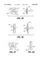
- Support member 4may be mounted on base 1 in a number of ways. It may be mounted to the surface of base 1 using solder, resins or other fixing techniques according to known practice. It may be mounted to other substrates, not shown in any figure, or it may be mounted in slots or trenches formed in base 1. Referring to FIG. 2a, support member 4 is mounted in trench 11 and fixed in position by an interference fit. In another example shown in FIG. 2b, support member 4 is mounted in trench 11 and held in place by solder 14 that is melted by resistive heating element 13.
- Optical fiber 5may be a single-mode or a multi-mode fiber of various known compositions. In many applications, performance is enhanced by forming a lens on the end of optical fiber 5 proximate to optical device 3; however, this feature is not required to practice the present invention. A separate lens, not shown in any figure, may also be used.
- Support member 6provides support for optical fiber 5 at a second position that is farther from optical component 3 than is the first position. It supports optical fiber 5 in a manner that restricts movement of the fiber in the X-Y plane. It need not restrict movement along the Z axis or rotation about the Z axis. Support member 6 may be constructed from a wide variety of materials and may be mounted to base 1 in a number of ways. Preferably, the CTE of support member 6 matches the CTE of support member 4.
- support member 4 and support member 6are identical; however, they may be very different.
- Support member 6may be formed and used according to known support techniques.
- the second position of support provided by support member 6can provide strain relief and it also can be used to adjust the alignment of optical fiber 5 more precisely than can be accomplished at the first position of support. The ability to make fine adjustments to alignment is discussed more fully below.
- Trench 7acts as a thermal barrier between optical component 3 and any soldering that may be used to construct and align device 10. It is not needed to practice the present invention.
- resistive heatersthat may be etched or otherwise formed into various components to assist in soldering, electrical leads to optical component 3, and electrical and thermal insulating pads.
- the first stepestablishes the first position of support near optical device 3 so as to achieve a substantially optimum alignment between optical fiber 5 and optical component 3.
- the first position of supportis established while operating optical device 3 and measuring performance so that changes in performance can be used to identify an optimum position.
- optical device 3is a laser, for example, light conveyed from the laser by optical fiber 5 is measured.
- optical device 3is a photodiode, for example, light received by the photodiode from optical fiber 5 is measured.
- the actual position of support member 4may shift slightly as the solder cools or the resin cures. Furthermore, if solder or some other high-temperature method is used and the CTE of various components are not properly matched, the position of optical component 3 may change relative to the first position of support as materials contract while cooling.
- the second step of a preferred alignment methodcorrects for these shifts in position by establishing the second position after the first position of support is established.
- optical fiber 5pivots about the first position of support as the second position of support is changed. Because the second position of support is farther away from optical component 3, shifts in position that occur as the second position is fixed do not degrade alignment as severely as do shifts in the first position.
- Positions of supportmay be established in a wide variety of ways, as discussed more fully below. Generally, these positions may be established by moving and fixing support members or, alternatively, support members with an appropriate structure may be fixed and optical fiber 5 moved appropriately and fixed to the support members.
- Optical fiber 5may be supported in a variety of ways that offer different advantages depending on the type of material that is used to construct the support.
- FIG. 3aOne way, illustrated in FIG. 3a, entails forming in support 42 a hole 41 that has a diameter essentially equal to the diameter of optical fiber 5.
- Support 42may be a support member mounted on base 1 as discussed above or it may be a carrier of optical fiber 5 that is attached to a support member. Various forms of carriers are discussed below.
- hole 41is tapered to facilitate insertion of optical fiber 5 into hole 41, and to minimize damage to the optical face of the fiber.
- the portion of support 42 that grips or contacts optical fiber 5extends along the length of the fiber by a distance that is no more than about one-third the fiber diameter.
- Single-mode optical fibersfor example, that are devoid of a jacket or protective covering typically have a diameter of about 125 microns ( ⁇ m).
- the precision required for the hole diameteris typically no more that about ⁇ 1 ⁇ m, which may be difficult to achieve with some manufacturing processes.
- Electrofoilsmay be formed with features such as holes that have dimensional tolerances less than one micron.
- electrofoilsare plated onto a number of photographically-produced conductive patterns formed on an electroform wafer. After the electrofoils have been plated to a desired thickness, they may be stripped away from the photographic patterns.
- the electrofoilsare formed with a thickness between 50 ⁇ m and 250 ⁇ m; however, dimensional precision deteriorates as the thickness increases.
- the electrolytic processmay impart a Gaussian distribution to the dimensions of the electrofoil across the electroform wafer.
- only components taken from a constant radius from the center of the waferwill have the same dimensions; therefore, the yields obtained by electroforming may not be high enough to make this technique cost effective.
- FIG. 3billustrates one structure that may be used to fix an optical fiber to support 42 with solder after the fiber has been aligned.
- Solder 43may be sputtered on to support 42, for example, and subsequently melted by a current passed between terminals 44 and 45. Fixation by solder or other means may be desirable to enhance the mechanical stability of the support but it is not required to practice the present invention.
- Another way to support optical fiber 5is by way of elastic members formed in materials like metallic foils.
- the formation of the elastic membersdoes not require as high a precision as the formation of a hole as discussed above because the range of deformation provided by the elastic members compensates for errors in the manufacturing process.
- low-cost high-volume manufacturing techniquescan be used to produce support members providing high-positional accuracy.
- FIGS. 5a through 5gSome examples are illustrated in FIGS. 5a through 5g.
- two slots in carrier 48aform elastic member 49a.
- member 49aWhen optical fiber 5 is inserted through opening 41 in the lower slot, it causes member 49a to deflect upward.
- the elastic property of the membercauses it to exert a force on optical fiber 5 in the direction of the arrow.
- support 48bcomprises elastic member 49b formed by two slots and circular opening 41 is formed in the lower slot to facilitate insertion of optical fiber 5.
- FIG. 5cthree slots in support 48c form two elastic members 49c.
- optical fiber 5is inserted through circular opening 41 between the members 49c, they are deflected away from one another and exert a force against the fiber.
- the tabs formed at the top of supports 48b and 48cmay be used to grip the supports when adjusting the alignment of optical fiber 5. This will be discussed further below.
- FIGS. 5d through 5gAdditional embodiments are shown in FIGS. 5d through 5g.
- three elastic members 49dare formed in a radial pattern around opening 41 in support 48d; the insertion of optical fiber 5 causes these elastic members to flex upward and out of the plane of support 48d, thereby exerting a force against optical fiber 5 and supporting it in position.
- two opposing elastic members 49eare formed on opposite sides of opening 41 in support 48e; the insertion of optical fiber 5 causes these elastic members to flex upward and out of the plane of support 48e, thereby exerting a force against optical fiber 5 and supporting it in position.
- three elastic members 49fare formed in an iris pattern around opening 41.
- FIG. 5fthree elastic members 49f are formed in an iris pattern around opening 41.
- one elastic member 49gis formed as a swinging arm.
- the insertion of optical fiber 5 in circular opening 41 in the channel to the left of elastic member 49gcauses it to deflect to the right, thereby exerting a force against optical fiber 5.
- these examplesshow, many variations are possible.
- the elastic membersapply a force against optical fiber 5 that is sufficient to restrain movement of the fiber in the X-Y plane, as shown in FIG. 1, yet allow the fiber to move along the Z axis and to rotate about the Z axis.
- Elastic membersmay also be formed in another way as illustrated in FIGS. 4a and 4b.
- opening 46is formed in support 42.
- a layer of elastic material 47is applied to support 42 so as to cover opening 46 and an opening 41 is formed in elastic coating 47.
- Opening 41is formed in such a way as to provide either a precision hole or one or more elastic members.
- FIGS. 4c through 4jAs these examples show, a wide variety of openings may be formed.
- Opening 46 as shown in FIG. 4ais rectangular. Rectangular shapes are convenient in many implementations; however, other shapes including but not limited to circles and ovals may be used to the practice of the present invention.
- opening 41is essentially a hole with a single slot.
- the examples in FIGS. 4d through 4fillustrate holes with varying numbers and widths of slots.
- a slot geometrymay be chosen to facilitate deformation of elastic material 47.
- opening 41is essentially a square with a single slot formed at one corner.
- the examples in FIGS. 4h through 4jillustrate squares with varying numbers, widths and orientations of slots. Many other configurations are possible.
- a wide variety of polyamidesmay be used to form the layer of elastic material 47, but no particular material is critical to the practice of the present invention.
- the important qualities for the layer of materialis that it be thin enough to facilitate formation of opening 41 yet be sufficiently strong and elastic to provide a stable support for optical fiber 5.
- FIG. 6illustrates supporting optical fiber 5 within opening 46 formed in support member 4.
- Carrier 51is formed on optical fiber 5, such as by metalization or by a metalized sheath.
- a means for fixing the position of optical fiber 5is applied to either or both of carrier 51 and support member 4 around opening 46. Opening 46 is formed in such a manner that optical fiber 5 is allowed to pivot. After optical fiber 5 is aligned, its position and orientation with respect to support member 4 is fixed.
- Fixation of the fibermay be accomplished in essentially any manner including the use of solder.
- resistive heater 141is formed around opening 46 and coupled terminals 142 and 143 are formed on either side of opening 46. This heater may be used to melt solder 145 deposited on support member 4, or to melt solder on carrier 51. Essentially any form of heating, such as by radiation, may be used. Carrier 51 can be eliminated if the solder that is used is able to bond directly to optical fiber 5.
- carrier 52provides direct support for optical fiber 5.
- carrier 52is in the form of support 48c shown in FIG. 5c.
- Carrier 52may be implemented in a wide variety of ways including the supports illustrated in FIGS. 3a and 3b, FIGS. 4a through 4j, and FIGS. 5a through 5g. No particular implementation is critical so long as it provides a stable support for optical fiber 5 and, preferably, permits some degree of pivoting around the position of support.
- carrier 52is manipulated or, alternatively, optical fiber 5 is manipulated directly to bring carrier 52 into contact with an external vertical surface of support member 4 and to align optical fiber 5 with optical component 3.
- carrier 52is bonded to a vertical surface of support member 4.
- the bondingmay be accomplished in essentially any manner such as by soldering. As shown in the figure, solder 145 is applied to support member 4 around opening 46 and resistive heater 141 is formed near opening 46 to facilitate melting solder 145. Alternatively, solder could be applied to carrier 52 and carrier 52 heated by some means such as radiation, thermal conduction or a current flowing through carrier 52.
- the alignment of optical fiber 5may be refined by subsequently establishing a second position of support at support member 6, as discussed above.
- the need for subsequent refinementis greatly reduced. Any shift in the first support position as the fiber is fixed, for example, as solder cools, will tend to be in the Z direction along the optical axis of optical fiber 5. Errors in alignment that are caused by shifts in the Z direction do not degrade optical performance nearly as much as errors that are caused by shifts in the X or the Y directions.
- Carrier 52may also be attached to an internal vertical surface of support member 4 in any of several ways. One of these ways is shown in FIG. 8, where slot 61 provides support member 4 with at least one internal vertical surface. Although it is anticipated that slot 61 will generally provide two internal vertical surfaces, there is no requirement that slot 61 provide more than one internal vertical surface for bonding. Carrier 52 may be formed according to any of the ways discussed above.
- FIG. 9aConstruction and alignment may be accomplished as shown in FIG. 9a.
- carrier 52is inserted into slot 61 so that opening 41 is exposed through opening 46, optical fiber 5 is inserted through opening 41, and then optical fiber 5 is aligned with optical component 3.
- carrier 52may be gripped and manipulated to align optical fiber 5.
- optical fiber 5may be gripped and manipulated directly.
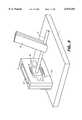
- FIG. 8illustrates tweezers 70 gripping optical fiber 5.
- FIG. 9billustrates additional detail for one embodiment of support member 4.
- This embodimentincludes two sections 81 made of silicon, ceramic or metal, for example. Each section contains trench 82 and opening 46. Support member 4 is formed by bonding together the two sections 81 so that the sides with trenches face one another to form slot 61. As shown in FIG. 9a, support member 4 may be mounted in a trench formed in base 1. If solder is used for mounting, it should have a higher melting temperature than any solder that is used to fix the alignment of optical fiber 5. For example, AuGe solder having a melting temperature of about 356° Celsius may be used to mount support member 4 to base 1, and AuSn solder having a melting temperature of about 286° Celsius may be used to fix the alignment of optical fiber 5.
- Carrier 52may be fixed to support member 4 by soldering it to a vertical surface in slot 61.
- the solderis applied to carrier 52 by sputtering, for example, before carrier 52 is inserted into slot 61.
- the embodiment illustrated in FIG. 8includes resistive heater 141 that may be used to melt this solder after alignment is achieved. The solder may be melted by heat obtained from any suitable source. In alternative embodiments, resistive heaters may be formed within trench 82 for either or both sections 81.
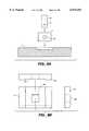
- Carrier 52may be fixed to support member 4 by force exerted on carrier 52 by opposing surfaces in slot 61. This may be accomplished by the embodiment shown in FIG. 10 which includes sections 83 and 84 with slot 61 formed between them in a manner similar to that described above. In this embodiment, however, the distance between the two sections in all or part of slot 61 is less than the thickness of carrier 52.
- Section 84includes resistive heater 141 and preferably is made of a material that has a CTE greater than the CTE of the material constituting section 83.
- section 84is heated by applying a current to heater 141. As the temperature of section 84 increases, section 84 expands to a greater extent than does section 83; however, because the two sections are bonded at their edges, section 84 bulges outward in the direction of arrow 85, causing the opposing faces in slot 61 to spread apart.
- Carrier 52is inserted into the slot, optical fiber 5 is inserted through hole 41 in carrier 52, and alignment is carried out as described above.
- currentis removed from heater 141 and section 83 is allowed to cool and return to its original shape. As it does so, the opposing faces in slot 61 come together and apply force on carrier 52, fixing it in position.
- carrier 52is also fixed by force from opposing internal faces in support member 4; however, in this embodiment, the opposing faces are spread apart by force.
- sections 87 and 88are not bonded together at the edges or top. Holes 89 are formed in section 88 so that pressure may be applied to the inside surface of section 87 and open a gap between the two sections. Carrier 52 is inserted into this gap. When alignment is achieved, pressure is released and section 87 returns to its original position, closing the gap and fixing the position of carrier 52.
- Soldermay also be used in the slot. As the solder cools, it contracts and pulls the opposing surfaces together to apply force to carrier 52 and fix it in position. In such an instance, the distance between the opposing surfaces of sections 87 and 88 can be a few microns wider than the thickness of carrier 52, facilitating manipulation of carrier 52. As the solder cools, the slot will be pulled together along the Z axis, applying holding force to carrier 52.
Landscapes
- Physics & Mathematics (AREA)
- General Physics & Mathematics (AREA)
- Optics & Photonics (AREA)
- Optical Couplings Of Light Guides (AREA)
Abstract
Description
Claims (36)
Priority Applications (1)
| Application Number | Priority Date | Filing Date | Title |
|---|---|---|---|
| US08/950,716US6074103A (en) | 1996-10-15 | 1997-10-15 | Aligning an optical fiber with electroluminescent semiconductor diodes and other optical components |
Applications Claiming Priority (3)
| Application Number | Priority Date | Filing Date | Title |
|---|---|---|---|
| US2837296P | 1996-10-15 | 1996-10-15 | |
| US4280997P | 1997-04-08 | 1997-04-08 | |
| US08/950,716US6074103A (en) | 1996-10-15 | 1997-10-15 | Aligning an optical fiber with electroluminescent semiconductor diodes and other optical components |
Publications (1)
| Publication Number | Publication Date |
|---|---|
| US6074103Atrue US6074103A (en) | 2000-06-13 |
Family
ID=27363257
Family Applications (1)
| Application Number | Title | Priority Date | Filing Date |
|---|---|---|---|
| US08/950,716Expired - Fee RelatedUS6074103A (en) | 1996-10-15 | 1997-10-15 | Aligning an optical fiber with electroluminescent semiconductor diodes and other optical components |
Country Status (1)
| Country | Link |
|---|---|
| US (1) | US6074103A (en) |
Cited By (30)
| Publication number | Priority date | Publication date | Assignee | Title |
|---|---|---|---|---|
| US20020033938A1 (en)* | 2000-09-21 | 2002-03-21 | Jenner Robert K. | Optical component plastic deformation control process |
| US20020043551A1 (en)* | 2000-08-25 | 2002-04-18 | Axsun Technologies, Inc. | Solid-phase welded optical element attach process |
| US6445858B1 (en)* | 2000-12-11 | 2002-09-03 | Jds Uniphase Inc. | Micro-alignment of optical components |
| US20020146227A1 (en)* | 2001-03-28 | 2002-10-10 | Makoto Suzuki | Collimator block for optical functional module |
| US6487355B1 (en)* | 1999-11-15 | 2002-11-26 | Axsun Technologies, Inc. | Mounting and alignment structures for optical components providing optical axis direction deformation |
| US6546172B2 (en) | 2001-02-20 | 2003-04-08 | Avanti Optics Corporation | Optical device |
| US6546173B2 (en) | 2001-02-20 | 2003-04-08 | Avanti Optics Corporation | Optical module |
| US20030075355A1 (en)* | 2000-12-26 | 2003-04-24 | Anderson Gene R. | An apparatus and method of using flexible printed circuit board in optical transceiver device |
| US20030081912A1 (en)* | 2001-10-31 | 2003-05-01 | Agilent Technologies, Inc. | Optical fibre alignment device and method |
| US6559464B1 (en) | 1999-11-15 | 2003-05-06 | Axsun Technologies, Inc. | Optical system active alignment process including alignment structure attach, position search, and deformation |
| US20030103738A1 (en)* | 2001-10-02 | 2003-06-05 | The Furukawa Electric Co., Ltd. | Optical fiber module |
| US6679636B1 (en)* | 2001-06-29 | 2004-01-20 | Network Elements, Inc. | Method and apparatus for maintaining alignment of a laser diode with an optical fiber |
| US20040114882A1 (en)* | 2002-12-12 | 2004-06-17 | Marquez Christian L. | Low cost integrated heater substrate for active optical fiber alignment |
| US6758610B2 (en) | 2001-12-10 | 2004-07-06 | Jds Uniphase Corporation | Optical component attachment to optoelectronic packages |
| US20040146253A1 (en)* | 2003-01-28 | 2004-07-29 | Wang Charlie X. | Method and apparatus for parallel optical transceiver module assembly |
| US6799902B2 (en) | 2000-12-26 | 2004-10-05 | Emcore Corporation | Optoelectronic mounting structure |
| US20040212802A1 (en)* | 2001-02-20 | 2004-10-28 | Case Steven K. | Optical device with alignment compensation |
| US20040223721A1 (en)* | 1999-11-15 | 2004-11-11 | Flanders Dale C. | Optical system production system |
| US20040264870A1 (en)* | 2002-08-20 | 2004-12-30 | Skunes Timothy A. | Optical alignment mount with height adjustment |
| US20050018972A1 (en)* | 2000-12-26 | 2005-01-27 | Anderson Gene R. | Housing and mounting structure |
| US20050123249A1 (en)* | 2003-12-05 | 2005-06-09 | Yun Ho G. | Structure for manufacturing optical module |
| US6905260B2 (en) | 2000-12-26 | 2005-06-14 | Emcore Corporation | Method and apparatus for coupling optical elements to optoelectronic devices for manufacturing optical transceiver modules |
| EP1390781A4 (en)* | 2001-04-03 | 2005-07-27 | Schott Optovance Inc | Device and method for positioning optical fibers |
| US6956999B2 (en)* | 2001-02-20 | 2005-10-18 | Cyberoptics Corporation | Optical device |
| US7021836B2 (en) | 2000-12-26 | 2006-04-04 | Emcore Corporation | Attenuator and conditioner |
| US20060205333A1 (en)* | 2002-04-19 | 2006-09-14 | Jorgen Zachariassen | Method and an apparatus for scalding slaughtered poultry |
| US7689091B1 (en)* | 2008-01-28 | 2010-03-30 | Newport Corporation | Unitary fiber clamp with flexible members and a member mover |
| US20100209053A1 (en)* | 2007-10-12 | 2010-08-19 | Thomas Moriarty | Optical fibre connector |
| US20110013869A1 (en)* | 2009-01-30 | 2011-01-20 | Bardia Pezeshki | Micromechanically aligned optical assembly |
| EP2878980A1 (en)* | 2013-11-27 | 2015-06-03 | Alcatel Lucent | Device for aligning and fastening an optical fiber coupled to an opto-electronic component |
Citations (22)
| Publication number | Priority date | Publication date | Assignee | Title |
|---|---|---|---|---|
| US4108529A (en)* | 1975-11-14 | 1978-08-22 | Sealectro Corporation | Electrical feedthrough devices |
| US4237474A (en)* | 1978-10-18 | 1980-12-02 | Rca Corporation | Electroluminescent diode and optical fiber assembly |
| US4342496A (en)* | 1980-05-22 | 1982-08-03 | Bunker Ramo Corporation | Contact assembly incorporating retaining means |
| US4702547A (en)* | 1986-07-28 | 1987-10-27 | Tektronix, Inc. | Method for attaching an optical fiber to a substrate to form an optical fiber package |
| US4798439A (en)* | 1985-03-29 | 1989-01-17 | British Telecommunications, Plc | Optical component mounting |
| US4803361A (en)* | 1986-05-26 | 1989-02-07 | Hitachi, Ltd. | Photoelectric device with optical fiber and laser emitting chip |
| US4883342A (en)* | 1983-08-22 | 1989-11-28 | Hitachi, Ltd. | Method of assembling a light emitting device with an optical fiber |
| US4884015A (en)* | 1985-06-17 | 1989-11-28 | Hitachi, Ltd. | Probing control method and apparatus for mechanism with multiple degrees of freedom |
| US4984866A (en)* | 1987-11-13 | 1991-01-15 | Societe Anonyme Dite: Alcatel Cit | Coupling device between in optical fiber and an opto-electronic component |
| US4997253A (en)* | 1989-04-03 | 1991-03-05 | Tektronix, Inc. | Electro-optical transducer module and a method of fabricating such a module |
| US5026138A (en)* | 1989-08-29 | 1991-06-25 | Gte Laboratories Incorporated | Multi-fiber alignment package for tilted facet optoelectronic components |
| US5029971A (en)* | 1988-03-02 | 1991-07-09 | British Telecommunications Public Limited Company | Optical fibre locating apparatus |
| US5307434A (en)* | 1992-07-16 | 1994-04-26 | At&T Bell Laboratories | Article that comprises a laser coupled to an optical fiber |
| US5425119A (en)* | 1993-09-23 | 1995-06-13 | Minnesota Mining And Manufacturing Company | Connector strain relief for optical fiber |
| US5430819A (en)* | 1993-12-21 | 1995-07-04 | At&T Corp. | Multiple optical fiber connector and method of making same |
| US5446810A (en)* | 1992-05-15 | 1995-08-29 | Sumitomo Electric Industries, Ltd. | Optical switch, optical fiber arranging member and method of manufacturing the optical fiber arranging member |
| US5469456A (en)* | 1994-03-31 | 1995-11-21 | Opto Power Corporation | Laser device and method of manufacture using non-metalized fiber |
| US5513290A (en)* | 1993-07-14 | 1996-04-30 | Sumitomo Electric Industries, Ltd. | Coupling structure of optical fibers and optical waveguides |
| US5537503A (en)* | 1993-10-25 | 1996-07-16 | Matsushita Electric Industrial Co., Ltd. | Optical semiconductor module and method of fabricating the same |
| US5611014A (en)* | 1994-12-07 | 1997-03-11 | Lucent Technologies Inc. | Optoelectronic device connecting techniques |
| US5793915A (en)* | 1997-07-03 | 1998-08-11 | Lucent Technologies Inc. | Thermal stress reduction in a laser module |
| US5857047A (en)* | 1996-03-20 | 1999-01-05 | The Regents Of The University Of California | Automated fiber pigtailing machine |
- 1997
- 1997-10-15USUS08/950,716patent/US6074103A/ennot_activeExpired - Fee Related
Patent Citations (22)
| Publication number | Priority date | Publication date | Assignee | Title |
|---|---|---|---|---|
| US4108529A (en)* | 1975-11-14 | 1978-08-22 | Sealectro Corporation | Electrical feedthrough devices |
| US4237474A (en)* | 1978-10-18 | 1980-12-02 | Rca Corporation | Electroluminescent diode and optical fiber assembly |
| US4342496A (en)* | 1980-05-22 | 1982-08-03 | Bunker Ramo Corporation | Contact assembly incorporating retaining means |
| US4883342A (en)* | 1983-08-22 | 1989-11-28 | Hitachi, Ltd. | Method of assembling a light emitting device with an optical fiber |
| US4798439A (en)* | 1985-03-29 | 1989-01-17 | British Telecommunications, Plc | Optical component mounting |
| US4884015A (en)* | 1985-06-17 | 1989-11-28 | Hitachi, Ltd. | Probing control method and apparatus for mechanism with multiple degrees of freedom |
| US4803361A (en)* | 1986-05-26 | 1989-02-07 | Hitachi, Ltd. | Photoelectric device with optical fiber and laser emitting chip |
| US4702547A (en)* | 1986-07-28 | 1987-10-27 | Tektronix, Inc. | Method for attaching an optical fiber to a substrate to form an optical fiber package |
| US4984866A (en)* | 1987-11-13 | 1991-01-15 | Societe Anonyme Dite: Alcatel Cit | Coupling device between in optical fiber and an opto-electronic component |
| US5029971A (en)* | 1988-03-02 | 1991-07-09 | British Telecommunications Public Limited Company | Optical fibre locating apparatus |
| US4997253A (en)* | 1989-04-03 | 1991-03-05 | Tektronix, Inc. | Electro-optical transducer module and a method of fabricating such a module |
| US5026138A (en)* | 1989-08-29 | 1991-06-25 | Gte Laboratories Incorporated | Multi-fiber alignment package for tilted facet optoelectronic components |
| US5446810A (en)* | 1992-05-15 | 1995-08-29 | Sumitomo Electric Industries, Ltd. | Optical switch, optical fiber arranging member and method of manufacturing the optical fiber arranging member |
| US5307434A (en)* | 1992-07-16 | 1994-04-26 | At&T Bell Laboratories | Article that comprises a laser coupled to an optical fiber |
| US5513290A (en)* | 1993-07-14 | 1996-04-30 | Sumitomo Electric Industries, Ltd. | Coupling structure of optical fibers and optical waveguides |
| US5425119A (en)* | 1993-09-23 | 1995-06-13 | Minnesota Mining And Manufacturing Company | Connector strain relief for optical fiber |
| US5537503A (en)* | 1993-10-25 | 1996-07-16 | Matsushita Electric Industrial Co., Ltd. | Optical semiconductor module and method of fabricating the same |
| US5430819A (en)* | 1993-12-21 | 1995-07-04 | At&T Corp. | Multiple optical fiber connector and method of making same |
| US5469456A (en)* | 1994-03-31 | 1995-11-21 | Opto Power Corporation | Laser device and method of manufacture using non-metalized fiber |
| US5611014A (en)* | 1994-12-07 | 1997-03-11 | Lucent Technologies Inc. | Optoelectronic device connecting techniques |
| US5857047A (en)* | 1996-03-20 | 1999-01-05 | The Regents Of The University Of California | Automated fiber pigtailing machine |
| US5793915A (en)* | 1997-07-03 | 1998-08-11 | Lucent Technologies Inc. | Thermal stress reduction in a laser module |
Non-Patent Citations (2)
| Title |
|---|
| S. Enochs, "A Packaging Technique to Achieve Stable Single-Mode Fiber to Laser Alignment," Proc. of SPIE, Sep. 1986, vol. 703, pp. 42-47. |
| S. Enochs, A Packaging Technique to Achieve Stable Single Mode Fiber to Laser Alignment, Proc. of SPIE, Sep. 1986, vol. 703, pp. 42 47.* |
Cited By (53)
| Publication number | Priority date | Publication date | Assignee | Title |
|---|---|---|---|---|
| US6625372B1 (en) | 1999-11-15 | 2003-09-23 | Axsun Technologies, Inc. | Mounting and alignment structures for optical components |
| US6559464B1 (en) | 1999-11-15 | 2003-05-06 | Axsun Technologies, Inc. | Optical system active alignment process including alignment structure attach, position search, and deformation |
| US20040223721A1 (en)* | 1999-11-15 | 2004-11-11 | Flanders Dale C. | Optical system production system |
| US7003211B2 (en) | 1999-11-15 | 2006-02-21 | Axsun Technologies, Inc. | Optical system production system |
| US6487355B1 (en)* | 1999-11-15 | 2002-11-26 | Axsun Technologies, Inc. | Mounting and alignment structures for optical components providing optical axis direction deformation |
| US20020043551A1 (en)* | 2000-08-25 | 2002-04-18 | Axsun Technologies, Inc. | Solid-phase welded optical element attach process |
| US6782180B2 (en)* | 2000-08-25 | 2004-08-24 | Axsun Technologies, Inc. | Reentrant alignment features for optical components |
| US6941631B2 (en) | 2000-09-21 | 2005-09-13 | Axsun Technologies, Inc. | Optical component plastic deformation control process |
| US20020033938A1 (en)* | 2000-09-21 | 2002-03-21 | Jenner Robert K. | Optical component plastic deformation control process |
| US6445858B1 (en)* | 2000-12-11 | 2002-09-03 | Jds Uniphase Inc. | Micro-alignment of optical components |
| US7021836B2 (en) | 2000-12-26 | 2006-04-04 | Emcore Corporation | Attenuator and conditioner |
| US20030075355A1 (en)* | 2000-12-26 | 2003-04-24 | Anderson Gene R. | An apparatus and method of using flexible printed circuit board in optical transceiver device |
| US6867377B2 (en) | 2000-12-26 | 2005-03-15 | Emcore Corporation | Apparatus and method of using flexible printed circuit board in optical transceiver device |
| US6905260B2 (en) | 2000-12-26 | 2005-06-14 | Emcore Corporation | Method and apparatus for coupling optical elements to optoelectronic devices for manufacturing optical transceiver modules |
| US6863444B2 (en) | 2000-12-26 | 2005-03-08 | Emcore Corporation | Housing and mounting structure |
| US20050018972A1 (en)* | 2000-12-26 | 2005-01-27 | Anderson Gene R. | Housing and mounting structure |
| US6799902B2 (en) | 2000-12-26 | 2004-10-05 | Emcore Corporation | Optoelectronic mounting structure |
| US20030219210A1 (en)* | 2001-02-20 | 2003-11-27 | Case Steven K. | Optical module |
| US7369334B2 (en) | 2001-02-20 | 2008-05-06 | Cyberoptics Corporation | Optical device with alignment compensation |
| US20040212802A1 (en)* | 2001-02-20 | 2004-10-28 | Case Steven K. | Optical device with alignment compensation |
| US7010855B2 (en) | 2001-02-20 | 2006-03-14 | Cyberoptics Corporation | Optical module |
| US6546172B2 (en) | 2001-02-20 | 2003-04-08 | Avanti Optics Corporation | Optical device |
| US6971164B2 (en) | 2001-02-20 | 2005-12-06 | Cyberoptics Corporation | Optical device |
| US6956999B2 (en)* | 2001-02-20 | 2005-10-18 | Cyberoptics Corporation | Optical device |
| US6546173B2 (en) | 2001-02-20 | 2003-04-08 | Avanti Optics Corporation | Optical module |
| US20020146227A1 (en)* | 2001-03-28 | 2002-10-10 | Makoto Suzuki | Collimator block for optical functional module |
| EP1390781A4 (en)* | 2001-04-03 | 2005-07-27 | Schott Optovance Inc | Device and method for positioning optical fibers |
| USRE41840E1 (en) | 2001-06-29 | 2010-10-19 | Ernest Charles Gilman | Method and apparatus for maintaining alignment of a laser diode with an optical fiber |
| US6679636B1 (en)* | 2001-06-29 | 2004-01-20 | Network Elements, Inc. | Method and apparatus for maintaining alignment of a laser diode with an optical fiber |
| US20030103738A1 (en)* | 2001-10-02 | 2003-06-05 | The Furukawa Electric Co., Ltd. | Optical fiber module |
| US6769817B2 (en)* | 2001-10-02 | 2004-08-03 | The Furukawa Electric Co., Ltd. | Optical fiber module |
| EP1308761A1 (en)* | 2001-10-31 | 2003-05-07 | Agilent Technologies, Inc. (a Delaware corporation) | Optical fibre alignment device and method |
| US6910811B2 (en) | 2001-10-31 | 2005-06-28 | Agilent Technologies, Inc. | Optical fiber alignment device and method |
| US20030081912A1 (en)* | 2001-10-31 | 2003-05-01 | Agilent Technologies, Inc. | Optical fibre alignment device and method |
| US6758610B2 (en) | 2001-12-10 | 2004-07-06 | Jds Uniphase Corporation | Optical component attachment to optoelectronic packages |
| US20060205333A1 (en)* | 2002-04-19 | 2006-09-14 | Jorgen Zachariassen | Method and an apparatus for scalding slaughtered poultry |
| US20040264870A1 (en)* | 2002-08-20 | 2004-12-30 | Skunes Timothy A. | Optical alignment mount with height adjustment |
| US20040114882A1 (en)* | 2002-12-12 | 2004-06-17 | Marquez Christian L. | Low cost integrated heater substrate for active optical fiber alignment |
| US6863453B2 (en) | 2003-01-28 | 2005-03-08 | Emcore Corporation | Method and apparatus for parallel optical transceiver module assembly |
| US20040146253A1 (en)* | 2003-01-28 | 2004-07-29 | Wang Charlie X. | Method and apparatus for parallel optical transceiver module assembly |
| US20050123249A1 (en)* | 2003-12-05 | 2005-06-09 | Yun Ho G. | Structure for manufacturing optical module |
| US7927023B2 (en)* | 2007-10-12 | 2011-04-19 | Firecomms Limited | Optical fibre connector |
| US20100209053A1 (en)* | 2007-10-12 | 2010-08-19 | Thomas Moriarty | Optical fibre connector |
| US7689091B1 (en)* | 2008-01-28 | 2010-03-30 | Newport Corporation | Unitary fiber clamp with flexible members and a member mover |
| US20110013869A1 (en)* | 2009-01-30 | 2011-01-20 | Bardia Pezeshki | Micromechanically aligned optical assembly |
| US8346037B2 (en) | 2009-01-30 | 2013-01-01 | Kaiam Corp. | Micromechanically aligned optical assembly |
| US8768119B2 (en) | 2009-01-30 | 2014-07-01 | Kaiam Corp. | Micromechanically aligned optical assembly |
| US8768120B2 (en) | 2009-01-30 | 2014-07-01 | Kaiam Corp. | Micromechanically aligned optical assembly |
| US9335481B2 (en) | 2009-01-30 | 2016-05-10 | Kaiam Corp. | Micromechanically aligned optical assembly |
| US9405072B2 (en) | 2009-01-30 | 2016-08-02 | Kaiam Corp. | Micromechanically aligned optical assembly |
| US9726836B2 (en) | 2009-01-30 | 2017-08-08 | Kaiam Corp. | Micromechanically aligned optical assembly |
| US10054748B2 (en) | 2009-01-30 | 2018-08-21 | Kaiam Corp. | Micromechanically aligned optical assembly |
| EP2878980A1 (en)* | 2013-11-27 | 2015-06-03 | Alcatel Lucent | Device for aligning and fastening an optical fiber coupled to an opto-electronic component |
Similar Documents
| Publication | Publication Date | Title |
|---|---|---|
| US6074103A (en) | Aligning an optical fiber with electroluminescent semiconductor diodes and other optical components | |
| US5870518A (en) | Microactuator for precisely aligning an optical fiber and an associated fabrication method | |
| US5602955A (en) | Microactuator for precisely aligning an optical fiber and an associated fabrication method | |
| US4888081A (en) | Device for positioning and fastening a lightwave guide to a base | |
| US4807956A (en) | Opto-electronic head for the coupling of a semi-conductor device with an optic fiber, and a method to align this semi-conductor device with this fiber | |
| EP0304118B1 (en) | Alignment of fibre arrays | |
| US5080458A (en) | Method and apparatus for positioning an optical fiber | |
| US5881198A (en) | Microactuator for precisely positioning an optical fiber and an associated method | |
| JPH0272642A (en) | Structure and method for connecting substrates | |
| JPH08204326A (en) | Method of arranging and soldering device | |
| US5533158A (en) | Electrostatic bonding of optical fibers to substrates | |
| EP0462742B1 (en) | Photonics module and alignment method | |
| JPS61240210A (en) | How to install optical elements | |
| US20050249464A1 (en) | Optical device with alignment compensation | |
| KR20060125721A (en) | MEMS-based contact conductive electrostatic chuck | |
| JPH02287307A (en) | Electric signal/light signal converting module and method for assembling the same | |
| WO2014123731A2 (en) | Interposer structure having optical fiber connection and related fiber optic connector for the same | |
| US6971164B2 (en) | Optical device | |
| JPH04233294A (en) | Device having board and unit | |
| US7010855B2 (en) | Optical module | |
| KR20030072001A (en) | Structure of flip chip bonding and method for bonding | |
| US5437092A (en) | Method of making contact areas on an optical waveguide | |
| US20240085635A1 (en) | Systems and methods of joining substrates using nano-particles | |
| US20030235388A1 (en) | Method for fabricating fiber blocks using solder as bonding material | |
| US6853779B2 (en) | Floating optical carrier |
Legal Events
| Date | Code | Title | Description |
|---|---|---|---|
| AS | Assignment | Owner name:SDL, INC., CALIFORNIA Free format text:ASSIGNMENT OF ASSIGNORS INTEREST;ASSIGNORS:HARGREAVES, DONALD C.;OLESKEVICH, TANYA K.;BARBER, RICHARD;REEL/FRAME:009091/0943;SIGNING DATES FROM 19980310 TO 19980316 | |
| FEPP | Fee payment procedure | Free format text:PAYOR NUMBER ASSIGNED (ORIGINAL EVENT CODE: ASPN); ENTITY STATUS OF PATENT OWNER: LARGE ENTITY | |
| AS | Assignment | Owner name:JDS UNIPHASE CORPORATION, CALIFORNIA Free format text:ASSIGNMENT OF ASSIGNORS INTEREST;ASSIGNOR:SDL, INC.;REEL/FRAME:013269/0920 Effective date:20020815 | |
| FEPP | Fee payment procedure | Free format text:PAYOR NUMBER ASSIGNED (ORIGINAL EVENT CODE: ASPN); ENTITY STATUS OF PATENT OWNER: LARGE ENTITY Free format text:PAYER NUMBER DE-ASSIGNED (ORIGINAL EVENT CODE: RMPN); ENTITY STATUS OF PATENT OWNER: LARGE ENTITY | |
| FPAY | Fee payment | Year of fee payment:4 | |
| FPAY | Fee payment | Year of fee payment:8 | |
| REMI | Maintenance fee reminder mailed | ||
| LAPS | Lapse for failure to pay maintenance fees | ||
| STCH | Information on status: patent discontinuation | Free format text:PATENT EXPIRED DUE TO NONPAYMENT OF MAINTENANCE FEES UNDER 37 CFR 1.362 | |
| FP | Lapsed due to failure to pay maintenance fee | Effective date:20120613 | |
| FEPP | Fee payment procedure | Free format text:PAYER NUMBER DE-ASSIGNED (ORIGINAL EVENT CODE: RMPN); ENTITY STATUS OF PATENT OWNER: LARGE ENTITY Free format text:PAYOR NUMBER ASSIGNED (ORIGINAL EVENT CODE: ASPN); ENTITY STATUS OF PATENT OWNER: LARGE ENTITY |