US6069905A - Vertical cavity surface emitting laser having intensity control - Google Patents
Vertical cavity surface emitting laser having intensity controlDownload PDFInfo
- Publication number
- US6069905A US6069905AUS09/001,894US189497AUS6069905AUS 6069905 AUS6069905 AUS 6069905AUS 189497 AUS189497 AUS 189497AUS 6069905 AUS6069905 AUS 6069905A
- Authority
- US
- United States
- Prior art keywords
- vcsel
- photo detector
- light
- window
- substrate
- Prior art date
- Legal status (The legal status is an assumption and is not a legal conclusion. Google has not performed a legal analysis and makes no representation as to the accuracy of the status listed.)
- Expired - Lifetime
Links
Images


Classifications
- H—ELECTRICITY
- H01—ELECTRIC ELEMENTS
- H01S—DEVICES USING THE PROCESS OF LIGHT AMPLIFICATION BY STIMULATED EMISSION OF RADIATION [LASER] TO AMPLIFY OR GENERATE LIGHT; DEVICES USING STIMULATED EMISSION OF ELECTROMAGNETIC RADIATION IN WAVE RANGES OTHER THAN OPTICAL
- H01S5/00—Semiconductor lasers
- H01S5/02—Structural details or components not essential to laser action
- H01S5/022—Mountings; Housings
- H01S5/0225—Out-coupling of light
- H01S5/02257—Out-coupling of light using windows, e.g. specially adapted for back-reflecting light to a detector inside the housing
- G—PHYSICS
- G02—OPTICS
- G02B—OPTICAL ELEMENTS, SYSTEMS OR APPARATUS
- G02B6/00—Light guides; Structural details of arrangements comprising light guides and other optical elements, e.g. couplings
- G02B6/24—Coupling light guides
- G02B6/42—Coupling light guides with opto-electronic elements
- G02B6/4201—Packages, e.g. shape, construction, internal or external details
- G02B6/4204—Packages, e.g. shape, construction, internal or external details the coupling comprising intermediate optical elements, e.g. lenses, holograms
- H—ELECTRICITY
- H01—ELECTRIC ELEMENTS
- H01S—DEVICES USING THE PROCESS OF LIGHT AMPLIFICATION BY STIMULATED EMISSION OF RADIATION [LASER] TO AMPLIFY OR GENERATE LIGHT; DEVICES USING STIMULATED EMISSION OF ELECTROMAGNETIC RADIATION IN WAVE RANGES OTHER THAN OPTICAL
- H01S5/00—Semiconductor lasers
- H01S5/02—Structural details or components not essential to laser action
- H01S5/022—Mountings; Housings
- H01S5/0225—Out-coupling of light
- H01S5/02251—Out-coupling of light using optical fibres
- H—ELECTRICITY
- H01—ELECTRIC ELEMENTS
- H01S—DEVICES USING THE PROCESS OF LIGHT AMPLIFICATION BY STIMULATED EMISSION OF RADIATION [LASER] TO AMPLIFY OR GENERATE LIGHT; DEVICES USING STIMULATED EMISSION OF ELECTROMAGNETIC RADIATION IN WAVE RANGES OTHER THAN OPTICAL
- H01S5/00—Semiconductor lasers
- H01S5/02—Structural details or components not essential to laser action
- H01S5/026—Monolithically integrated components, e.g. waveguides, monitoring photo-detectors, drivers
- H01S5/0262—Photo-diodes, e.g. transceiver devices, bidirectional devices
- H01S5/0264—Photo-diodes, e.g. transceiver devices, bidirectional devices for monitoring the laser-output
- H—ELECTRICITY
- H01—ELECTRIC ELEMENTS
- H01S—DEVICES USING THE PROCESS OF LIGHT AMPLIFICATION BY STIMULATED EMISSION OF RADIATION [LASER] TO AMPLIFY OR GENERATE LIGHT; DEVICES USING STIMULATED EMISSION OF ELECTROMAGNETIC RADIATION IN WAVE RANGES OTHER THAN OPTICAL
- H01S5/00—Semiconductor lasers
- H01S5/06—Arrangements for controlling the laser output parameters, e.g. by operating on the active medium
- H01S5/068—Stabilisation of laser output parameters
- H01S5/0683—Stabilisation of laser output parameters by monitoring the optical output parameters
- H—ELECTRICITY
- H01—ELECTRIC ELEMENTS
- H01S—DEVICES USING THE PROCESS OF LIGHT AMPLIFICATION BY STIMULATED EMISSION OF RADIATION [LASER] TO AMPLIFY OR GENERATE LIGHT; DEVICES USING STIMULATED EMISSION OF ELECTROMAGNETIC RADIATION IN WAVE RANGES OTHER THAN OPTICAL
- H01S5/00—Semiconductor lasers
- H01S5/10—Construction or shape of the optical resonator, e.g. extended or external cavity, coupled cavities, bent-guide, varying width, thickness or composition of the active region
- H01S5/18—Surface-emitting [SE] lasers, e.g. having both horizontal and vertical cavities
- H01S5/183—Surface-emitting [SE] lasers, e.g. having both horizontal and vertical cavities having only vertical cavities, e.g. vertical cavity surface-emitting lasers [VCSEL]
Definitions
- the inventionpertains to vertical cavity surface emitting lasers (VCSEL's), and particularly to VCSEL's having a constant output. More particularly, the invention pertains to VCSEL's having power output monitors and feedback power control mechanisms.
- VCSEL'svertical cavity surface emitting lasers
- a photo detector or diode, reflective window and feedback deviceare used to detect, monitor and control the vertical cavity surface emitting laser (VCSEL) output to overcome above-noted problems.
- the photo detector or diodeshould be compatible with integral packaging and be inexpensive. Compact packaging with electrical and capacitive isolation between the VCSEL and the photo detector is necessary as is proper attention to optical effects, such as polarization, that can interfere with the proportionality between the feedback and the output.
- the present inventionincludes a diode structure which is a silicon photo detector used for monitoring the power output of the VCSEL.
- the photo detectoris a monolithic structure having an active junction area for collection of an optical signal and an isolated pad area for mounting the VCSEL.
- the VCSELis ideally suited for mounting directly on top of the photo detector.
- the photo detector, with the VCSEL attached,is mounted on a header and covered by a can with a tilted window.
- the windowis about 0.01 inches thick and may be made from glass or other appropriate material such as sapphire.
- the windowis coated for reflecting some of the light emitted from the VCSEL back to the detector and for inhibiting external light from entering the can.
- the coatingis made of material composed of a noble metal with low complex refractive index dispersion at the operating wavelength, for example, platinum or palladium at 850 nanometers.
- the coatingis of the order of 100 angstroms thick.
- the tilted window can for a VCSELis intended for use with the off-center photo detector or diode sub-mount.
- the angle of the windowis set such that the coherent light from the VCSEL top surface strikes the active area of the off-center photo detector or diode sub-mount without shadowing by the VCSEL chip itself.
- the tracking ratiois rendered independent of changes in the output pattern of the VCSEL due to changes in drive current and temperature. This device also allows the effective use of a larger fraction of the VCSEL's on a wafer by utilizing the constant tracking ratio to apply feedback to the combination of the VCSEL and its drive circuit.
- Tracking ratiois defined as the ratio of the power coupled to the fiber optic waveguide to the response of the back monitor photo detector or diode. It is necessary that the height and angle of the tilt window can be compatible with the height of the VCSEL chip as well as the size and location of the optically sensitive area of the offset photo detector or diode.
- the dimensions and angle of the tilt window disclosed hereare one specific design and do not represent limitations of this general device. There is an approach for partially overcoming the shadowing of the VCSEL chip by using reflections from both surfaces of a flat window having a centered photo detector or diode. However, the tilt window can provides a more constant tracking ratio than the flat window can. There is an alternate, but more expensive, approach for illuminating the off-center photo detector or diode by using a grating lens on a flat window VCSEL can.
- FIGS. 1a and 1breveals a layout of a VCSEL and the photo detector for monitoring power.
- FIG. 2is a schematic of the feedback electronics for the invention.
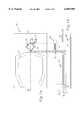
- FIG. 3shows the structure of the VCSEL, detector and the encompassing can package.
- FIG. 4the patterns of reflected VCSEL light on the detector area.
- FIG. 5is an example of polarization sensitivity versus reflection angle that for transmitted light that can occur in a reflective configuration designed for power monitoring.
- FIGS. 6a and 6breveal the polarization effects of a metallic reflective surface on a tilted window.
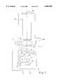
- FIG. 7shows the housing layout for the invention.
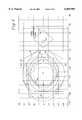
- FIG. 1aOne layout of a mounting pad 11 and terminal pad 12 for a VCSEL 10, situated in a photo detector area 13 of integrated circuit 14 is illustrated by FIG. 1a.
- the proportionality of photo detector area 13 relative to pad area 11is not to scale.
- FIG. 1bwhich is a cross section A--A of FIG. 1a
- the active junction area 13 for collecting the reflected optical signalis formed by a planar P-type diffusion 15 into an N-type silicon substrate 16. Diffused region 15 is the anode of photo detector 13 and substrate 16 is the cathode.
- VCSEL 10is mounted on an isolated pad area 11 which is isolated from N-type substrate 16 by a deposited oxide 17, an oxide/nitride anti-reflection coating 18 and a grown oxide 19.
- Pads 11 and 12 and connecting strip 20may be fabricated from gold.
- Diffusion depth 20 of P-type region 15is appropriate for high collection efficiency of photo detector 13.
- P-type region 15is covered with thin grown oxide 19 and anti-reflection coating 18 which is optimized for collection of photons at the wavelength and incidence angle of the reflected optical signal, and also designed to minimize the difference between collection of P- and S-polarized radiation.
- N-type silicon substrate 16may be homogeneous, epitaxial or wafer bond material.
- Pad 11, on which a VCSEL 10 cathode 21 is mounted,is isolated from substrate with a dielectric coating 17. Thickness 22 of dielectric coatings 17 and 19 is maximized to decrease capacitance between VCSEL 10 and substrate 16.
- the dielectricis formed by a combination of thermally grown oxide 19 and deposited oxide 17.
- the backside of the N-type substrate 16is covered with a dielectric layer 23 for isolation from the header of the containing can package.
- an N+ type diffusion 24is formed on the top edge or border of substrate 16.
- a limitation of the deviceis non-linearity of tracking between a feedback signal 28 and a VCSEL 10 output 29.
- Diode 13senses the received laser 10 output 29 to convert it into transmitted signal 30.
- Signal 30is amplified or buffered by amplifier 26 into signal 31 which goes into the inverting input of differential amplifier 27.
- a reference voltage signal 32goes to the noninverting input of amplifier 27.
- the output of amplifier 27is a feedback signal 28 that goes to variable current source 25 that adjusts the amount of current to VCSEL 10 to control power output 29 of VCSEL 10 in accordance with feedback signal 28.
- the geometric pattern of the laser outputvaries with power output 29, such that the ratio of the feedback signal 28 to the transmitted signal 30 is not constant as a function of power or intensity of output light 29.
- a device 33is designed to provide linear tracking.
- the solutionis to use a can package 34 having a window 37 which is tilted at an angle ⁇ with respect to silicon die 14 to direct a reflected light pattern 36 from partially reflective surface 37, as shown in FIG. 3.
- the active junction area 10is positioned with respect to the VCSEL pad 14 which is geometrically designed so as to assure collection of light from an entire reflected pattern 36, including tolerances.
- coating 18 over the active region 13must be designed so as to minimize polarization sensitivity. Again, thick dielectric 17 under pad 11 reduces VCSEL-to-substrate capacitance.
- the response time of a photo detector fabricated with a homogeneous substrateis limited by transit time and/or the RC (resistor-capacitor) time constant.
- the response timemay be substantially improved by the use of an epitaxial or wafer bond substrate.
- di.e., the diameter of the major axis
- sis the distance between VCSEL 10 and monitor 13 center lines
- his the height of reflective surface 37 above monitor or photo detector 13
- Lis the height of monitor 13 above VCSEL 10
- ⁇is half of the angle of the VCSEL 10 emission cone.
- the spotmust be within the detector 13 to avoid overfill, and shadowing should not be possible.
- FIG. 5shows the relative locations of active detector area 13 and VCSEL 10 mounting pad 11. This layout may be different for different configurations. Any pattern from the reflection of a cone from a tilted window will be elliptical.
- the variant ellipses of FIG. 4can be attained through intentional adjustment of window tilt and position, as described below, but the main reason to model the variants is to establish the active area shape affording the best packaging tolerance.
- VCSEL 10emits light 29 in a form of an emission cone having an angle of 2 ⁇ .
- a portion 36 of light 29is reflected onto detector area 13 as in a nominal pattern 38 with reflective window 37 having a nominal tilt angle ⁇ .
- the pattern of portion 36 of VCSEL light 29may be adjusted with tilt angle ⁇ , distance s, height h, length L, and rotation r of window 37 and can 34 relative to detector 13 and VCSEL 10.
- Optional patterns 41, 42, 43 and 44may be utilized.
- FIG. 4shows ellipses 38 and 40 as an approach leading to appropriate active area shapes, of reflected light 36 on active detector area 13.
- Ellipse pattern 38may be adjusted to be like ellipse patterns 41-44.
- Ellipse pattern 38has 0.15 NA rays which correspond to a 17 degree VCSEL emission cone. (NA is the trigonometric sine of the half-angle of the emission cone; e.g., 2arcsin 0.15 is approximately 17 degrees.)
- ellipse pattern 40has 0.12 NA rays which correspond to a 14 degree VCSEL emission cone.
- Corresponding patterns like patterns 41-44are not shown for ellipse pattern 40.
- Various patterns evolving from nominal ellipse 38are effected through adjustments of tilt, distance and rotation.
- the following examplesare the result of a variation of just one parameter of the settings for nominal pattern 38.
- Ellipse 41is the result of reducing d by 8 mils and ellipse 45 is the result of increasing d by 8 mils.
- Ellipse 46is the result of a 14 degree angle ⁇ of tilt window 37 relative to die 14, and ellipse 42 is the result of a 20 degree angle ⁇ tilt.
- Ellipse 43is the result of a positive ten degree rotation of tilted window 37 relative to VCSEL 10 and detector 13, and ellipse 44 is the result of a negative ten degree rotation.
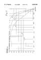
- a graph of FIG. 5shows the polarization sensitivity at the photo detector or diode 13 surface. This polarization is an issue which is minimized by the present invention.
- the incident angle of the reflective beamis twice the mirror 37 tilt angle ⁇ .
- the graphshows intensity transmission of light through window 37 versus the incident angle of light 29 in degrees.
- An anti-reflective coatingis on the surface of the window 37.
- the incident mediais air, the light wavelength is 850 nanometers (nm), and the substrate is silicon.
- Curve 47shows the transmission of S-polarized light; curve 48 shows the transmission of P-polarized light; and curve 49 shows the average transmission of both S- and P-polarized light.
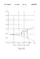
- the graphs of FIGS. 6a and 6breveal the polarization effects of a metallic reflective surface on tilted window 37. Any tilted reflector results in some polarization sensitivity; however, an appropriate thickness and proper choice of materials of the metallic coating on window 37 minimizes the polarization effects. Reflection from a metallic surface is polarization independent until the reflecting film is thin enough to transmit light. A 95-angstrom-thick Pt (platinum) produces about 5 dB of attenuation and results in polarization curves 52, 53, and 54 of graph 6a, which show intensity reflection versus incident angle in degrees for reflection of P- and S-polarized light, and average reflected light, respectively.
- the monitor powerwould be increased by the 23 percent difference in reflection; the feedback loop, shown in FIG. 2, would decrease the emitted power to compensate; and the transmittance would be reduced by a further 15 percent so the power emitted outside the package would be reduced to 0.85/1.23, or 69 percent of its previous value. (This is a worst-case number since complete polarization-flipping is rare in VCSEL's.) To avoid such dramatic power fluctuations, the angle of the window must be held to the minimum consistent with other constraints of package and photo detector or diode sizes.
- Device 33may be inserted in a housing 40, as shown in FIG. 7, for coupling light 29 to another device via an optical fiber or other medium.
- the fiberfor instance, may be inserted into opening 39 of housing 40.
- Light 29can be focused by lens 35 for entry into the optical fiber.
Landscapes
- Physics & Mathematics (AREA)
- General Physics & Mathematics (AREA)
- Optics & Photonics (AREA)
- Condensed Matter Physics & Semiconductors (AREA)
- Electromagnetism (AREA)
- Semiconductor Lasers (AREA)
Abstract
Description
Claims (16)
Priority Applications (2)
| Application Number | Priority Date | Filing Date | Title |
|---|---|---|---|
| US09/001,894US6069905A (en) | 1997-12-31 | 1997-12-31 | Vertical cavity surface emitting laser having intensity control |
| PCT/US1998/025487WO1999034487A1 (en) | 1997-12-31 | 1998-12-02 | Vertical cavity surface emitting laser having intensity |
Applications Claiming Priority (1)
| Application Number | Priority Date | Filing Date | Title |
|---|---|---|---|
| US09/001,894US6069905A (en) | 1997-12-31 | 1997-12-31 | Vertical cavity surface emitting laser having intensity control |
Publications (1)
| Publication Number | Publication Date |
|---|---|
| US6069905Atrue US6069905A (en) | 2000-05-30 |
Family
ID=21698327
Family Applications (1)
| Application Number | Title | Priority Date | Filing Date |
|---|---|---|---|
| US09/001,894Expired - LifetimeUS6069905A (en) | 1997-12-31 | 1997-12-31 | Vertical cavity surface emitting laser having intensity control |
Country Status (2)
| Country | Link |
|---|---|
| US (1) | US6069905A (en) |
| WO (1) | WO1999034487A1 (en) |
Cited By (45)
| Publication number | Priority date | Publication date | Assignee | Title |
|---|---|---|---|---|
| US6339496B1 (en) | 1999-06-22 | 2002-01-15 | University Of Maryland | Cavity-less vertical semiconductor optical amplifier |
| US20020057883A1 (en)* | 2000-09-29 | 2002-05-16 | Kevin Malone | High speed optical subassembly with ceramic carrier |
| US6452669B1 (en)* | 1998-08-31 | 2002-09-17 | Digital Optics Corp. | Transmission detection for vertical cavity surface emitting laser power monitor and system |
| US20030002129A1 (en)* | 1999-12-13 | 2003-01-02 | Okihiro Kobayashi | Optical acoustoelectric transducer |
| US20030076864A1 (en)* | 2001-10-23 | 2003-04-24 | Hironobu Sai | Surface light emitting type semiconductor laser having a vertical cavity |
| US6567435B1 (en) | 1999-03-19 | 2003-05-20 | Optical Communication Products, Inc. | VCSEL power monitoring system using plastic encapsulation techniques |
| US20030123508A1 (en)* | 2001-12-28 | 2003-07-03 | Werner Thomas R. | Integral vertical cavity surface emitting laser and power monitor |
| US6600845B1 (en)* | 1999-10-18 | 2003-07-29 | Digital Optics Corporation | Integrated parallel transmitter |
| US6624899B1 (en)* | 2000-06-29 | 2003-09-23 | Schmitt Measurement Systems, Inc. | Triangulation displacement sensor |
| US6654125B2 (en) | 2002-04-04 | 2003-11-25 | Inlight Solutions, Inc | Method and apparatus for optical spectroscopy incorporating a vertical cavity surface emitting laser (VCSEL) as an interferometer reference |
| US6697396B2 (en) | 2001-10-02 | 2004-02-24 | Honeywell International Inc. | Laser light sources having integrated detector and intensity control and methods of producing same |
| US6845118B1 (en)* | 1999-01-25 | 2005-01-18 | Optical Communication Products, Inc. | Encapsulated optoelectronic devices with controlled properties |
| US20050073690A1 (en)* | 2003-10-03 | 2005-04-07 | Abbink Russell E. | Optical spectroscopy incorporating a vertical cavity surface emitting laser (VCSEL) |
| US20050084218A1 (en)* | 2003-09-08 | 2005-04-21 | Seiko Epson Corporation | Optical module, and optical transmission device |
| US20050151082A1 (en)* | 2004-01-13 | 2005-07-14 | Coffin John M. | Stabilized infrared source for infrared spectrometers |
| US20050180698A1 (en)* | 2004-02-12 | 2005-08-18 | Ralf Hauffe | Light transmitting modules with optical power monitoring |
| US6963598B1 (en)* | 2000-05-23 | 2005-11-08 | Finisar Corporation | System and method for VCSEL polarization control |
| US20060086947A1 (en)* | 2004-10-25 | 2006-04-27 | Johnson Christopher W | Securing a transistor outline can within an optical component |
| US7068694B2 (en)* | 2003-06-02 | 2006-06-27 | Rohm Co., Ltd. | Mold type semiconductor laser |
| US20060192221A1 (en)* | 2002-08-16 | 2006-08-31 | Jds Uniphase Corporation | Methods, apparatus, and systems with semiconductor laser packaging for high modulation bandwidth |
| US20060227844A1 (en)* | 2005-04-11 | 2006-10-12 | Guenter James K | On-chip lenses for diverting vertical cavity surface emitting laser beams |
| US20070063140A1 (en)* | 2005-09-22 | 2007-03-22 | Honeywell International Inc. | Optical particulate sensor in oil quality detection |
| US20070131842A1 (en)* | 2005-12-12 | 2007-06-14 | Xerox Corporation | External laser power monitor using pickoff mirror in a ROS |
| US20080232422A1 (en)* | 2005-11-02 | 2008-09-25 | Stephen Sutton | Laser Radiation Source |
| US20100002235A1 (en)* | 2008-07-07 | 2010-01-07 | IRMicrosystems SA | Laser diode arrangements and method for gas detection |
| US20100046348A1 (en)* | 2008-08-19 | 2010-02-25 | Takami Iwafuji | Optical module, optical communication device using the same and reflective optical path setting method |
| WO2010096781A1 (en)* | 2009-02-20 | 2010-08-26 | Brenner Mary K | Direct modulated modified vertical cavity surface emitting lasers |
| DE102010003034A1 (en)* | 2010-03-18 | 2011-09-22 | Vertilas Gmbh | light unit |
| US20120262071A1 (en)* | 2011-02-14 | 2012-10-18 | Arkalumen Inc. | Lighting apparatus and method for detecting reflected light from local objects |
| US20130155390A1 (en)* | 2011-12-15 | 2013-06-20 | Earl Jensen | Film thickness monitor |
| DE102012205308A1 (en)* | 2012-03-30 | 2013-10-02 | Trumpf Laser- Und Systemtechnik Gmbh | Device for amplifying a laser beam |
| US20150098481A1 (en)* | 2010-08-31 | 2015-04-09 | University Of Central Florida Research Foundation, Inc. | Optical signal amplification |
| US9510420B2 (en) | 2010-05-11 | 2016-11-29 | Arkalumen, Inc. | Methods and apparatus for causing LEDs to generate light output comprising a modulated signal |
| US9565727B2 (en) | 2011-03-25 | 2017-02-07 | Arkalumen, Inc. | LED lighting apparatus with first and second colour LEDs |
| CN106848829A (en)* | 2017-04-17 | 2017-06-13 | 武汉盛为芯科技股份有限公司 | A kind of vertical-cavity surface-emitting coaxial packaging photoelectric device and its method for packing |
| US9756692B2 (en) | 2010-05-11 | 2017-09-05 | Arkalumen, Inc. | Methods and apparatus for communicating current levels within a lighting apparatus incorporating a voltage converter |
| US9775211B2 (en) | 2015-05-05 | 2017-09-26 | Arkalumen Inc. | Circuit and apparatus for controlling a constant current DC driver output |
| US20180011267A1 (en)* | 2016-07-08 | 2018-01-11 | Finisar Corporation | Chip on leadframe optical subassembly |
| US9992836B2 (en) | 2015-05-05 | 2018-06-05 | Arkawmen Inc. | Method, system and apparatus for activating a lighting module using a buffer load module |
| US9992829B2 (en) | 2015-05-05 | 2018-06-05 | Arkalumen Inc. | Control apparatus and system for coupling a lighting module to a constant current DC driver |
| US10225904B2 (en) | 2015-05-05 | 2019-03-05 | Arkalumen, Inc. | Method and apparatus for controlling a lighting module based on a constant current level from a power source |
| US10568180B2 (en) | 2015-05-05 | 2020-02-18 | Arkalumen Inc. | Method and apparatus for controlling a lighting module having a plurality of LED groups |
| DE102018214803A1 (en)* | 2018-08-31 | 2020-03-05 | Robert Bosch Gmbh | Device for coupling electromagnetic waves into a chip |
| US10757784B2 (en) | 2011-07-12 | 2020-08-25 | Arkalumen Inc. | Control apparatus and lighting apparatus with first and second voltage converters |
| US11631959B2 (en)* | 2020-04-07 | 2023-04-18 | Nichia Corporation | Light-emitting device |
Families Citing this family (4)
| Publication number | Priority date | Publication date | Assignee | Title |
|---|---|---|---|---|
| EP1604229A4 (en)* | 2003-03-14 | 2007-04-18 | Pbc Lasers Ltd | Apparatus for generating improved laser beam |
| FR2915029A1 (en) | 2007-04-13 | 2008-10-17 | Commissariat Energie Atomique | COMPACT OPTOELECTRONIC DEVICE INCLUDING AT LEAST ONE SURFACE-EMITTING LASER |
| CN104505708A (en)* | 2014-12-16 | 2015-04-08 | 昂纳信息技术(深圳)有限公司 | Vertical cavity surface emitting laser component |
| CN109586160B (en)* | 2017-09-29 | 2020-10-30 | 光环科技股份有限公司 | High-speed vertical resonant cavity surface emitting laser packaging structure |
Citations (8)
| Publication number | Priority date | Publication date | Assignee | Title |
|---|---|---|---|---|
| GB2300031A (en)* | 1995-04-21 | 1996-10-23 | Emhart Inc | Retainer for a blind rivet nut assembly |
| US5606572A (en)* | 1994-03-24 | 1997-02-25 | Vixel Corporation | Integration of laser with photodiode for feedback control |
| EP0786839A1 (en)* | 1996-01-23 | 1997-07-30 | Samsung Electronics Co., Ltd. | Light output apparatus and optical pickup apparatus employing the same |
| EP0805528A2 (en)* | 1996-04-29 | 1997-11-05 | Motorola, Inc. | Reflection power monitoring system for vertical cavity surface emitting lasers |
| US5737348A (en)* | 1996-10-28 | 1998-04-07 | Honeywell Inc. | Light source monitor with compensated tracking ratio |
| US5761229A (en)* | 1996-01-25 | 1998-06-02 | Hewlett-Packard Company | Integrated controlled intensity laser-based light source |
| US5812582A (en)* | 1995-10-03 | 1998-09-22 | Methode Electronics, Inc. | Vertical cavity surface emitting laser feedback system and method |
| US5835514A (en)* | 1996-01-25 | 1998-11-10 | Hewlett-Packard Company | Laser-based controlled-intensity light source using reflection from a convex surface and method of making same |
Family Cites Families (1)
| Publication number | Priority date | Publication date | Assignee | Title |
|---|---|---|---|---|
| KR100259490B1 (en)* | 1995-04-28 | 2000-06-15 | 윤종용 | Photodetector integrated surface light laser and optical pickup device using same |
- 1997
- 1997-12-31USUS09/001,894patent/US6069905A/ennot_activeExpired - Lifetime
- 1998
- 1998-12-02WOPCT/US1998/025487patent/WO1999034487A1/enactiveApplication Filing
Patent Citations (8)
| Publication number | Priority date | Publication date | Assignee | Title |
|---|---|---|---|---|
| US5606572A (en)* | 1994-03-24 | 1997-02-25 | Vixel Corporation | Integration of laser with photodiode for feedback control |
| GB2300031A (en)* | 1995-04-21 | 1996-10-23 | Emhart Inc | Retainer for a blind rivet nut assembly |
| US5812582A (en)* | 1995-10-03 | 1998-09-22 | Methode Electronics, Inc. | Vertical cavity surface emitting laser feedback system and method |
| EP0786839A1 (en)* | 1996-01-23 | 1997-07-30 | Samsung Electronics Co., Ltd. | Light output apparatus and optical pickup apparatus employing the same |
| US5761229A (en)* | 1996-01-25 | 1998-06-02 | Hewlett-Packard Company | Integrated controlled intensity laser-based light source |
| US5835514A (en)* | 1996-01-25 | 1998-11-10 | Hewlett-Packard Company | Laser-based controlled-intensity light source using reflection from a convex surface and method of making same |
| EP0805528A2 (en)* | 1996-04-29 | 1997-11-05 | Motorola, Inc. | Reflection power monitoring system for vertical cavity surface emitting lasers |
| US5737348A (en)* | 1996-10-28 | 1998-04-07 | Honeywell Inc. | Light source monitor with compensated tracking ratio |
Cited By (85)
| Publication number | Priority date | Publication date | Assignee | Title |
|---|---|---|---|---|
| US6452669B1 (en)* | 1998-08-31 | 2002-09-17 | Digital Optics Corp. | Transmission detection for vertical cavity surface emitting laser power monitor and system |
| US6845118B1 (en)* | 1999-01-25 | 2005-01-18 | Optical Communication Products, Inc. | Encapsulated optoelectronic devices with controlled properties |
| US6567435B1 (en) | 1999-03-19 | 2003-05-20 | Optical Communication Products, Inc. | VCSEL power monitoring system using plastic encapsulation techniques |
| US6339496B1 (en) | 1999-06-22 | 2002-01-15 | University Of Maryland | Cavity-less vertical semiconductor optical amplifier |
| US6600845B1 (en)* | 1999-10-18 | 2003-07-29 | Digital Optics Corporation | Integrated parallel transmitter |
| US7391976B2 (en)* | 1999-12-13 | 2008-06-24 | Kabushiki Kaisha Kenwood | Optical acoustoelectric transducer |
| US20030002129A1 (en)* | 1999-12-13 | 2003-01-02 | Okihiro Kobayashi | Optical acoustoelectric transducer |
| US6630994B2 (en) | 2000-04-12 | 2003-10-07 | Digital Optics Corp. | Transmission detection for a laser power monitor and system |
| US6963598B1 (en)* | 2000-05-23 | 2005-11-08 | Finisar Corporation | System and method for VCSEL polarization control |
| US6624899B1 (en)* | 2000-06-29 | 2003-09-23 | Schmitt Measurement Systems, Inc. | Triangulation displacement sensor |
| US6888169B2 (en) | 2000-09-29 | 2005-05-03 | Optical Communication Products, Inc. | High speed optical subassembly with ceramic carrier |
| US20060162104A1 (en)* | 2000-09-29 | 2006-07-27 | Optical Communication Products, Inc. | High speed optical sub-assembly with ceramic carrier |
| WO2002027874A3 (en)* | 2000-09-29 | 2003-08-14 | Cielo Communications Inc | High speed optical subassembly with ceramic carrier |
| US20050189549A1 (en)* | 2000-09-29 | 2005-09-01 | Kevin Malone | High speed optical subassembly with ceramic carrier |
| US7045824B2 (en) | 2000-09-29 | 2006-05-16 | Optical Communication Products, Inc. | High speed optical subassembly with ceramic carrier |
| US20020057883A1 (en)* | 2000-09-29 | 2002-05-16 | Kevin Malone | High speed optical subassembly with ceramic carrier |
| US6697396B2 (en) | 2001-10-02 | 2004-02-24 | Honeywell International Inc. | Laser light sources having integrated detector and intensity control and methods of producing same |
| US6856635B2 (en)* | 2001-10-23 | 2005-02-15 | Rohm Co., Ltd. | Surface light emitting type semiconductor laser having a vertical cavity |
| US20030076864A1 (en)* | 2001-10-23 | 2003-04-24 | Hironobu Sai | Surface light emitting type semiconductor laser having a vertical cavity |
| US7085300B2 (en) | 2001-12-28 | 2006-08-01 | Finisar Corporation | Integral vertical cavity surface emitting laser and power monitor |
| US20030123508A1 (en)* | 2001-12-28 | 2003-07-03 | Werner Thomas R. | Integral vertical cavity surface emitting laser and power monitor |
| US6654125B2 (en) | 2002-04-04 | 2003-11-25 | Inlight Solutions, Inc | Method and apparatus for optical spectroscopy incorporating a vertical cavity surface emitting laser (VCSEL) as an interferometer reference |
| US20060192221A1 (en)* | 2002-08-16 | 2006-08-31 | Jds Uniphase Corporation | Methods, apparatus, and systems with semiconductor laser packaging for high modulation bandwidth |
| US7068694B2 (en)* | 2003-06-02 | 2006-06-27 | Rohm Co., Ltd. | Mold type semiconductor laser |
| CN100352115C (en)* | 2003-06-02 | 2007-11-28 | 罗姆股份有限公司 | Mold type semiconductor laser |
| US7113658B2 (en) | 2003-09-08 | 2006-09-26 | Seiko Epson Corporation | Optical module, and optical transmission device |
| US20050084218A1 (en)* | 2003-09-08 | 2005-04-21 | Seiko Epson Corporation | Optical module, and optical transmission device |
| US20050073690A1 (en)* | 2003-10-03 | 2005-04-07 | Abbink Russell E. | Optical spectroscopy incorporating a vertical cavity surface emitting laser (VCSEL) |
| US20050151082A1 (en)* | 2004-01-13 | 2005-07-14 | Coffin John M. | Stabilized infrared source for infrared spectrometers |
| US7119904B2 (en)* | 2004-01-13 | 2006-10-10 | Thermo Electron Scientific Instruments Corporation | Stabilized infrared source for infrared spectrometers |
| US7467897B2 (en) | 2004-02-12 | 2008-12-23 | Hymite A/S | Light transmitting modules with optical power monitoring |
| US20050180698A1 (en)* | 2004-02-12 | 2005-08-18 | Ralf Hauffe | Light transmitting modules with optical power monitoring |
| US7165896B2 (en) | 2004-02-12 | 2007-01-23 | Hymite A/S | Light transmitting modules with optical power monitoring |
| US20070091608A1 (en)* | 2004-02-12 | 2007-04-26 | Hymite A/S | Light Transmitting Modules With Optical Power Monitoring |
| US20080311689A1 (en)* | 2004-10-25 | 2008-12-18 | Finisar Corporation | Securing a transistor outline can within an optical component |
| US7785930B2 (en)* | 2004-10-25 | 2010-08-31 | Finisar Corporation | Securing a transistor outline can within an optical component |
| US20060086947A1 (en)* | 2004-10-25 | 2006-04-27 | Johnson Christopher W | Securing a transistor outline can within an optical component |
| US7476905B2 (en)* | 2004-10-25 | 2009-01-13 | Finisar Corporation | Securing a transistor outline can within an optical component |
| US7460578B2 (en)* | 2005-04-11 | 2008-12-02 | Finisar Corporation | On-chip lenses for diverting vertical cavity surface emitting laser beams |
| US20060227844A1 (en)* | 2005-04-11 | 2006-10-12 | Guenter James K | On-chip lenses for diverting vertical cavity surface emitting laser beams |
| US7321117B2 (en) | 2005-09-22 | 2008-01-22 | Honeywell International Inc. | Optical particulate sensor in oil quality detection |
| US20070063140A1 (en)* | 2005-09-22 | 2007-03-22 | Honeywell International Inc. | Optical particulate sensor in oil quality detection |
| US20080232422A1 (en)* | 2005-11-02 | 2008-09-25 | Stephen Sutton | Laser Radiation Source |
| US20070131842A1 (en)* | 2005-12-12 | 2007-06-14 | Xerox Corporation | External laser power monitor using pickoff mirror in a ROS |
| US7253386B2 (en) | 2005-12-12 | 2007-08-07 | Xerox Corporation | Method and apparatus for monitoring and controlling laser intensity in a ROS scanning system |
| US20100002235A1 (en)* | 2008-07-07 | 2010-01-07 | IRMicrosystems SA | Laser diode arrangements and method for gas detection |
| US20100046348A1 (en)* | 2008-08-19 | 2010-02-25 | Takami Iwafuji | Optical module, optical communication device using the same and reflective optical path setting method |
| WO2010096781A1 (en)* | 2009-02-20 | 2010-08-26 | Brenner Mary K | Direct modulated modified vertical cavity surface emitting lasers |
| DE102010003034A1 (en)* | 2010-03-18 | 2011-09-22 | Vertilas Gmbh | light unit |
| RU2516032C1 (en)* | 2010-03-18 | 2014-05-20 | Вертилаз Гмбх | Light-emitting module |
| US8773663B2 (en) | 2010-03-18 | 2014-07-08 | Vertilas Gmbh | Luminous unit |
| US9756692B2 (en) | 2010-05-11 | 2017-09-05 | Arkalumen, Inc. | Methods and apparatus for communicating current levels within a lighting apparatus incorporating a voltage converter |
| US9510420B2 (en) | 2010-05-11 | 2016-11-29 | Arkalumen, Inc. | Methods and apparatus for causing LEDs to generate light output comprising a modulated signal |
| US9601902B2 (en)* | 2010-08-31 | 2017-03-21 | University Of Central Florida Research Foundation, Inc. | Optical signal amplification |
| US20150098481A1 (en)* | 2010-08-31 | 2015-04-09 | University Of Central Florida Research Foundation, Inc. | Optical signal amplification |
| US20120262071A1 (en)* | 2011-02-14 | 2012-10-18 | Arkalumen Inc. | Lighting apparatus and method for detecting reflected light from local objects |
| US9192009B2 (en)* | 2011-02-14 | 2015-11-17 | Arkalumen Inc. | Lighting apparatus and method for detecting reflected light from local objects |
| US9565727B2 (en) | 2011-03-25 | 2017-02-07 | Arkalumen, Inc. | LED lighting apparatus with first and second colour LEDs |
| US10251229B2 (en) | 2011-03-25 | 2019-04-02 | Arkalumen Inc. | Light engine and lighting apparatus with first and second groups of LEDs |
| US10939527B2 (en) | 2011-03-25 | 2021-03-02 | Arkalumen Inc. | Light engine configured to be between a power source and another light engine |
| US9918362B2 (en) | 2011-03-25 | 2018-03-13 | Arkalumen Inc. | Control unit and lighting apparatus including light engine and control unit |
| US10568170B2 (en) | 2011-03-25 | 2020-02-18 | Arkalumen Inc. | Lighting apparatus with a plurality of light engines |
| US10757784B2 (en) | 2011-07-12 | 2020-08-25 | Arkalumen Inc. | Control apparatus and lighting apparatus with first and second voltage converters |
| US20130155390A1 (en)* | 2011-12-15 | 2013-06-20 | Earl Jensen | Film thickness monitor |
| US9360302B2 (en)* | 2011-12-15 | 2016-06-07 | Kla-Tencor Corporation | Film thickness monitor |
| US9306367B2 (en)* | 2012-03-30 | 2016-04-05 | Trumpf Lasersystems For Semiconductor Manufacturing Gmbh | Device for amplifying a laser beam |
| US20130272327A1 (en)* | 2012-03-30 | 2013-10-17 | Trumpf Laser- Und Systemtechnik Gmbh | Device for Amplifying a Laser Beam |
| DE102012205308A1 (en)* | 2012-03-30 | 2013-10-02 | Trumpf Laser- Und Systemtechnik Gmbh | Device for amplifying a laser beam |
| DE102012205308B4 (en)* | 2012-03-30 | 2018-05-30 | Trumpf Lasersystems For Semiconductor Manufacturing Gmbh | Device for amplifying a laser beam |
| US9775211B2 (en) | 2015-05-05 | 2017-09-26 | Arkalumen Inc. | Circuit and apparatus for controlling a constant current DC driver output |
| US11083062B2 (en) | 2015-05-05 | 2021-08-03 | Arkalumen Inc. | Lighting apparatus with controller for generating indication of dimming level for DC power source |
| US9992829B2 (en) | 2015-05-05 | 2018-06-05 | Arkalumen Inc. | Control apparatus and system for coupling a lighting module to a constant current DC driver |
| US10225904B2 (en) | 2015-05-05 | 2019-03-05 | Arkalumen, Inc. | Method and apparatus for controlling a lighting module based on a constant current level from a power source |
| US9992836B2 (en) | 2015-05-05 | 2018-06-05 | Arkawmen Inc. | Method, system and apparatus for activating a lighting module using a buffer load module |
| US10568180B2 (en) | 2015-05-05 | 2020-02-18 | Arkalumen Inc. | Method and apparatus for controlling a lighting module having a plurality of LED groups |
| US20180011267A1 (en)* | 2016-07-08 | 2018-01-11 | Finisar Corporation | Chip on leadframe optical subassembly |
| US10295768B2 (en)* | 2016-07-08 | 2019-05-21 | Finisar Corporation | Chip on leadframe optical subassembly |
| CN106848829A (en)* | 2017-04-17 | 2017-06-13 | 武汉盛为芯科技股份有限公司 | A kind of vertical-cavity surface-emitting coaxial packaging photoelectric device and its method for packing |
| DE102018214803A1 (en)* | 2018-08-31 | 2020-03-05 | Robert Bosch Gmbh | Device for coupling electromagnetic waves into a chip |
| US10921533B2 (en) | 2018-08-31 | 2021-02-16 | Robert Bosch Gmbh | Method for coupling electromagnetic waves into a chip using a cavity for a light source and an opening, for passage of light of the light source, which is connected to the cavity |
| DE102018214803B4 (en) | 2018-08-31 | 2021-09-02 | Robert Bosch Gmbh | Device for coupling electromagnetic waves into a chip |
| US11631959B2 (en)* | 2020-04-07 | 2023-04-18 | Nichia Corporation | Light-emitting device |
| US11955768B2 (en)* | 2020-04-07 | 2024-04-09 | Nichia Corporation | Light-emitting device |
| US20240154383A1 (en)* | 2020-04-07 | 2024-05-09 | Nichia Corporation | Light-emitting device |
| US12316069B2 (en)* | 2020-04-07 | 2025-05-27 | Nichia Corporation | Light-emitting device |
Also Published As
| Publication number | Publication date |
|---|---|
| WO1999034487A1 (en) | 1999-07-08 |
Similar Documents
| Publication | Publication Date | Title |
|---|---|---|
| US6069905A (en) | Vertical cavity surface emitting laser having intensity control | |
| US6567435B1 (en) | VCSEL power monitoring system using plastic encapsulation techniques | |
| US4983009A (en) | Light transmitting device utilizing indirect reflection | |
| US6314117B1 (en) | Laser diode package | |
| US5835514A (en) | Laser-based controlled-intensity light source using reflection from a convex surface and method of making same | |
| US5479426A (en) | Semiconductor laser device with integrated reflector on a (511) tilted lattice plane silicon substrate | |
| US5771254A (en) | Integrated controlled intensity laser-based light source | |
| US5761229A (en) | Integrated controlled intensity laser-based light source | |
| US5793785A (en) | Semiconductor laser device | |
| CA2241388A1 (en) | Optical source with monitor | |
| JP2892820B2 (en) | Semiconductor laser device | |
| US6630994B2 (en) | Transmission detection for a laser power monitor and system | |
| Sawada et al. | Hybrid microlaser encoder | |
| US7767947B2 (en) | Semiconductor light source with optical feedback | |
| US7067854B2 (en) | Optical receiver | |
| JP2892812B2 (en) | Semiconductor laser device | |
| JP2003101133A (en) | Light emitting module | |
| JPH11274654A (en) | Semiconductor laser device | |
| JP3032376B2 (en) | Semiconductor laser device | |
| JP3169917B2 (en) | Semiconductor laser device | |
| JP3140085B2 (en) | Semiconductor laser device | |
| CA2297898A1 (en) | Semiconductor laser power monitoring arrangements and method | |
| US4380074A (en) | Integrated circuit laser and electro-optical amplifier | |
| JPH05327131A (en) | Semiconductor laser device | |
| KR100532326B1 (en) | Semiconductor optical package |
Legal Events
| Date | Code | Title | Description |
|---|---|---|---|
| AS | Assignment | Owner name:HONEYWELL INC., MINNESOTA Free format text:ASSIGNMENT OF ASSIGNORS INTEREST;ASSIGNORS:GUENTER, JAMES K.;DAVIS, RICHARD A.;MATZEN, WALTER T.;AND OTHERS;REEL/FRAME:009721/0734;SIGNING DATES FROM 19981109 TO 19981113 | |
| STCF | Information on status: patent grant | Free format text:PATENTED CASE | |
| FEPP | Fee payment procedure | Free format text:PAYOR NUMBER ASSIGNED (ORIGINAL EVENT CODE: ASPN); ENTITY STATUS OF PATENT OWNER: LARGE ENTITY | |
| FPAY | Fee payment | Year of fee payment:4 | |
| AS | Assignment | Owner name:FINISAR CORPORATION, CALIFORNIA Free format text:ASSIGNMENT OF ASSIGNORS INTEREST;ASSIGNOR:HONEYWELL INTERNATIONAL, INC.;REEL/FRAME:014468/0371 Effective date:20040301 Owner name:FINISAR CORPORATION, CALIFORNIA Free format text:ASSIGNMENT OF ASSIGNORS INTEREST;ASSIGNOR:HONEYWELL INTERNATIONAL, INC.;REEL/FRAME:014468/0407 Effective date:20040301 Owner name:FINISAR CORPORATION, CALIFORNIA Free format text:ASSIGNMENT OF ASSIGNORS INTEREST;ASSIGNOR:HONEYWELL INTERNATIONAL, INC.;REEL/FRAME:014484/0171 Effective date:20040301 | |
| AS | Assignment | Owner name:FINISAR CORPORATION, CALIFORNIA Free format text:ASSIGNMENT OF ASSIGNORS INTEREST;ASSIGNOR:HONEYWELL INTERNATIONAL, INC.;REEL/FRAME:014499/0365 Effective date:20040301 | |
| FPAY | Fee payment | Year of fee payment:8 | |
| FPAY | Fee payment | Year of fee payment:12 | |
| AS | Assignment | Owner name:II-VI DELAWARE, INC., DELAWARE Free format text:ASSIGNMENT OF ASSIGNORS INTEREST;ASSIGNOR:FINISAR CORPORATION;REEL/FRAME:052286/0001 Effective date:20190924 |