US6069804A - Bi-directional dc-to-dc power converter - Google Patents
Bi-directional dc-to-dc power converterDownload PDFInfo
- Publication number
- US6069804A US6069804AUS09/359,499US35949999AUS6069804AUS 6069804 AUS6069804 AUS 6069804AUS 35949999 AUS35949999 AUS 35949999AUS 6069804 AUS6069804 AUS 6069804A
- Authority
- US
- United States
- Prior art keywords
- output
- input
- terminal
- control signal
- winding
- Prior art date
- Legal status (The legal status is an assumption and is not a legal conclusion. Google has not performed a legal analysis and makes no representation as to the accuracy of the status listed.)
- Expired - Lifetime
Links
Images


Classifications
- H—ELECTRICITY
- H02—GENERATION; CONVERSION OR DISTRIBUTION OF ELECTRIC POWER
- H02J—CIRCUIT ARRANGEMENTS OR SYSTEMS FOR SUPPLYING OR DISTRIBUTING ELECTRIC POWER; SYSTEMS FOR STORING ELECTRIC ENERGY
- H02J7/00—Circuit arrangements for charging or depolarising batteries or for supplying loads from batteries
- H02J7/0068—Battery or charger load switching, e.g. concurrent charging and load supply
- H—ELECTRICITY
- H02—GENERATION; CONVERSION OR DISTRIBUTION OF ELECTRIC POWER
- H02M—APPARATUS FOR CONVERSION BETWEEN AC AND AC, BETWEEN AC AND DC, OR BETWEEN DC AND DC, AND FOR USE WITH MAINS OR SIMILAR POWER SUPPLY SYSTEMS; CONVERSION OF DC OR AC INPUT POWER INTO SURGE OUTPUT POWER; CONTROL OR REGULATION THEREOF
- H02M3/00—Conversion of DC power input into DC power output
- H02M3/22—Conversion of DC power input into DC power output with intermediate conversion into AC
- H02M3/24—Conversion of DC power input into DC power output with intermediate conversion into AC by static converters
- H02M3/28—Conversion of DC power input into DC power output with intermediate conversion into AC by static converters using discharge tubes with control electrode or semiconductor devices with control electrode to produce the intermediate AC
- H02M3/325—Conversion of DC power input into DC power output with intermediate conversion into AC by static converters using discharge tubes with control electrode or semiconductor devices with control electrode to produce the intermediate AC using devices of a triode or a transistor type requiring continuous application of a control signal
- H02M3/335—Conversion of DC power input into DC power output with intermediate conversion into AC by static converters using discharge tubes with control electrode or semiconductor devices with control electrode to produce the intermediate AC using devices of a triode or a transistor type requiring continuous application of a control signal using semiconductor devices only
- H02M3/33569—Conversion of DC power input into DC power output with intermediate conversion into AC by static converters using discharge tubes with control electrode or semiconductor devices with control electrode to produce the intermediate AC using devices of a triode or a transistor type requiring continuous application of a control signal using semiconductor devices only having several active switching elements
- H02M3/33576—Conversion of DC power input into DC power output with intermediate conversion into AC by static converters using discharge tubes with control electrode or semiconductor devices with control electrode to produce the intermediate AC using devices of a triode or a transistor type requiring continuous application of a control signal using semiconductor devices only having several active switching elements having at least one active switching element at the secondary side of an isolation transformer
- H02M3/33584—Bidirectional converters
- H—ELECTRICITY
- H02—GENERATION; CONVERSION OR DISTRIBUTION OF ELECTRIC POWER
- H02M—APPARATUS FOR CONVERSION BETWEEN AC AND AC, BETWEEN AC AND DC, OR BETWEEN DC AND DC, AND FOR USE WITH MAINS OR SIMILAR POWER SUPPLY SYSTEMS; CONVERSION OF DC OR AC INPUT POWER INTO SURGE OUTPUT POWER; CONTROL OR REGULATION THEREOF
- H02M3/00—Conversion of DC power input into DC power output
- H02M3/22—Conversion of DC power input into DC power output with intermediate conversion into AC
- H02M3/24—Conversion of DC power input into DC power output with intermediate conversion into AC by static converters
- H02M3/28—Conversion of DC power input into DC power output with intermediate conversion into AC by static converters using discharge tubes with control electrode or semiconductor devices with control electrode to produce the intermediate AC
- H02M3/325—Conversion of DC power input into DC power output with intermediate conversion into AC by static converters using discharge tubes with control electrode or semiconductor devices with control electrode to produce the intermediate AC using devices of a triode or a transistor type requiring continuous application of a control signal
- H02M3/335—Conversion of DC power input into DC power output with intermediate conversion into AC by static converters using discharge tubes with control electrode or semiconductor devices with control electrode to produce the intermediate AC using devices of a triode or a transistor type requiring continuous application of a control signal using semiconductor devices only
- H02M3/33569—Conversion of DC power input into DC power output with intermediate conversion into AC by static converters using discharge tubes with control electrode or semiconductor devices with control electrode to produce the intermediate AC using devices of a triode or a transistor type requiring continuous application of a control signal using semiconductor devices only having several active switching elements
- H02M3/33576—Conversion of DC power input into DC power output with intermediate conversion into AC by static converters using discharge tubes with control electrode or semiconductor devices with control electrode to produce the intermediate AC using devices of a triode or a transistor type requiring continuous application of a control signal using semiconductor devices only having several active switching elements having at least one active switching element at the secondary side of an isolation transformer
- H02M3/33592—Conversion of DC power input into DC power output with intermediate conversion into AC by static converters using discharge tubes with control electrode or semiconductor devices with control electrode to produce the intermediate AC using devices of a triode or a transistor type requiring continuous application of a control signal using semiconductor devices only having several active switching elements having at least one active switching element at the secondary side of an isolation transformer having a synchronous rectifier circuit or a synchronous freewheeling circuit at the secondary side of an isolation transformer
- H—ELECTRICITY
- H02—GENERATION; CONVERSION OR DISTRIBUTION OF ELECTRIC POWER
- H02M—APPARATUS FOR CONVERSION BETWEEN AC AND AC, BETWEEN AC AND DC, OR BETWEEN DC AND DC, AND FOR USE WITH MAINS OR SIMILAR POWER SUPPLY SYSTEMS; CONVERSION OF DC OR AC INPUT POWER INTO SURGE OUTPUT POWER; CONTROL OR REGULATION THEREOF
- H02M1/00—Details of apparatus for conversion
- H02M1/0083—Converters characterised by their input or output configuration
- H02M1/009—Converters characterised by their input or output configuration having two or more independently controlled outputs
- Y—GENERAL TAGGING OF NEW TECHNOLOGICAL DEVELOPMENTS; GENERAL TAGGING OF CROSS-SECTIONAL TECHNOLOGIES SPANNING OVER SEVERAL SECTIONS OF THE IPC; TECHNICAL SUBJECTS COVERED BY FORMER USPC CROSS-REFERENCE ART COLLECTIONS [XRACs] AND DIGESTS
- Y02—TECHNOLOGIES OR APPLICATIONS FOR MITIGATION OR ADAPTATION AGAINST CLIMATE CHANGE
- Y02B—CLIMATE CHANGE MITIGATION TECHNOLOGIES RELATED TO BUILDINGS, e.g. HOUSING, HOUSE APPLIANCES OR RELATED END-USER APPLICATIONS
- Y02B70/00—Technologies for an efficient end-user side electric power management and consumption
- Y02B70/10—Technologies improving the efficiency by using switched-mode power supplies [SMPS], i.e. efficient power electronics conversion e.g. power factor correction or reduction of losses in power supplies or efficient standby modes
Definitions
- the subject inventionrelates to the field of pulse-width-modulated dc-to-dc switching converters and more particularly to that class of switching converter referred to as a flyback converter.
- dc-to-dc convertersWhile operating into a fixed load, and when powered from a substantially fixed input source of voltage, dc-to-dc converters typically operate in one of three modes. The three modes of operation are the discontinuous conduction mode, the critical conduction mode and the continuous conduction mode.
- the invention bi-directional dc-to-dc power converteris designed to operate in the continuous conduction mode in which the composite sum of the load current plus the magnetizing current is circulating through the input transformer's (coupled inductor's) input winding or output winding exclusively depending on whether the input or output bi-directional switch is on.
- the present inventionis directed to an improved flyback converter in which energy is re-circulated through the converter's flyback transformer windings in a controlled manner to eliminate the need for pre-load or bleeder resistors on the output(s) and to provide enhanced cross regulation on lightly loaded multiple output windings.
- dc-to-dc power convertersare typically provided with bleeder resistors that provide a minimum guaranteed load to prevent the output voltage from increasing at light load and to reduce the likelihood of a temporary spike on the output in the event of normal load interruption.
- the control loop bandwidthis limited and if a converter were operating at 50-150 kHz, a number of power cycles might be produced after the interruption of the load before the duty cycle on-time could be reduced, resulting in a jump in voltage on an unloaded output.
- a bleedercontributes to loss of efficiency.
- Flyback dc-to-dc power converters having multiple output windingstypically have bleeder resistors on all outputs for the same reason as above and also because energy stored in the leakage inductance of the primary is coupled to the secondary windings and voltage on an isolated unloaded secondary output will continue to rise with the interruption of a normal load if there is no bleeder. Bleeders are also used on multiple outputs to enhance cross regulation.
- a bi-directional dc-to-dc power converterhaving an input coupled to an input voltage source such as a battery or rectified and filtered ac line source.
- the bi-directional dc-to-dc power converterhas an output coupled to an output voltage source such as a charged filter capacitor or a battery.
- the convertercomprises at least two bi-directional switches, an input bi-directional switch such as a power FET having a conduction channel between its drain and source, and a control terminal such as a gate, and an output bi-directional switch, such as a power FET, having a conduction channel and a control terminal such as a gate.
- the bi-directional dc-to-dc power converterhas a coupled inductor, such as a flyback transformer, having an input winding and at least one output winding.
- the coupled inductor input windingis tightly coupled to the output winding.
- the coupled inductor input windingis connected in series with the input voltage source and the input bi-directional switch conduction channel.
- the coupled inductor output windingis connected in series with the output voltage source and the output bi-directional switch conduction channel.
- a clock circuit with a substantially fixed clock periodprovides first and second control signals such as the drive signals that reach the gates of FETs 28 and 34 in FIG. 7. Each control signal has a first and second state.
- the second control signalhas a state that is the complement of the state of the first control signal.
- the first control signalWhen the first control signal is high, the second is low and vice versa.
- the first control signal first state durationis followed by the second control signal first state duration substantially forming the clock period.
- the first control signal's first state portion of the total periodis referred to as its duty ratio, D, and the remaining portion is referred to as D'.
- the first control signalis coupled to the input bi-directional switch control terminal, such as the gate of FET 28, and the second control signal is coupled to the output bi-directional switch control terminal, such as the gate of FET 34.
- the input bi-directional switch conduction channelsuch as the channel of FET 28, is driven into a conductive state in response to the first control signal being in a first state, such as a high state, and into a non-conductive state in response to the first control signal being in a second state, such as a low state or ground state.
- the output bi-directional switch conduction channelsuch as the channel of FET 34, is driven into a conductive state in response to the second control signal being in a first state, such as a high or positive state and into a non-conductive state in response to the second control signal being in a second state, or low state.
- the first and second control signalsdrive the respective switches so that one switch or the other is on at all times and in such a way that the switches can conduct current in either direction.
- the coupled inductorhas at least two output windings.
- the coupled inductor input windingis tightly coupled to each output winding.
- Each output windingis coupled to an output voltage source, such as a capacitor and load as described for the first embodiment.
- Each voltage sourceconducts through its respective output bi-directional switch during the D' control signal interval, as necessary, to enhance cross regulation or to support continuous operation during a temporary interruption of power from the input voltage source.
- At least one output windingis coupled to a battery and at least a second output winding is coupled to an output voltage source, such as a capacitor and load as described for the first embodiment.
- An input bi-directional switchhas a conduction channel and a control terminal, such as a gate.
- At least a first and second output bi-directional switcheach have a conduction channel and a control terminal, such as a gate.
- a clock circuitprovides a first and second control signal as in the first embodiment. The second control signal is connected to the first and second output bi-directional switch control terminals.
- the first and second output bi-directional switch conduction channelsare driven into a conductive state in response to the second control signal being in a first state and into a non-conductive state in response to the second control signal being in a second state such as ground.
- the first output windingis coupled in series with the battery and the first output bi-directional switch conduction channel.
- the second output windingis coupled in series with the output voltage source and the second output bi-directional switch conduction channel.
- a control circuit meansfor providing a clock signal with a fixed period to set the output of a latch to a first state, the output of the latch driving the first control signal high, sensing the output voltage of the converter, comparing a portion of the output voltage with a precision internal reference voltage to provide an error voltage, sensing the input winding current rise in the input winding as a ramp current voltage, comparing the ramp current voltage with the error voltage, providing a reset signal to the latch to zero set the latch to a second state in response to the ramp current voltage exceeding the error voltage, the zero set output of the latch driving the first control signal low, the latch being set to the first state on receiving the next clock signal.
- a fifth alternative embodimentuses a resonant transition control means for sensing the coupled inductor input and output winding currents and the output voltage and for adjusting the clock frequency to provide operation in a resonant transition mode and to adjust the output voltage to a predetermined level.
- a controlled bi-directional current regulatorsuch as a resistor connected in parallel with a blocking diode is added in series with the battery to enable the battery to be continually charged.
- the batteryconducts through a second blocking diode or alternatively, a boost converter, to provide power to its respective output as necessary to enhance cross regulation or to support continuous operation during a temporary interruption of power from the input voltage source.
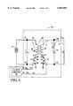
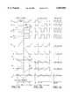
- FIG. 1is a schematic diagram of the major elements in a bi-directional dc-to-dc power converter having an input coupled to an input voltage source and an output connected to a first output voltage source;
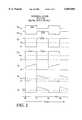
- FIG. 2is a timing diagram for the bi-directional dc-to-dc power converter operating with a normal load and with a 50% duty cycle;
- FIG. 3is a timing diagram for the bi-directional dc-to-dc power converter operating with a no load and with a 50% duty cycle;
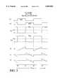
- FIG. 4is a timing diagram for the bi-directional dc-to-dc power converter operating with a normal load and with a 25% duty cycle;
- FIG. 5is a timing diagram for the bi-directional dc-to-dc power converter operating with no load and with a 25% duty cycle;
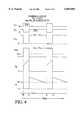
- FIGS. 6a-6cshow three timing diagram charts for each of three load conditions for a bi-directional dc-to-dc power converter adjusted to provide resonant transitions on both the input and output bi-directional switches;
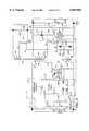
- FIG. 7is a schematic diagram of the bi-directional dc-to-dc power converter showing a first and second output winding each respective output winding being connected in series with a respective bi-directional switch and a respective voltage source;
- FIG. 8is a schematic diagram of the bi-directional dc-to-dc power converter of FIG. 7 with the addition of components necessary for a controlled directional current regulator in series with the battery and the second output winding 64,
- FIG. 9is a schematic diagram of the bi-directional dc-to-dc power converter showing the use of a UC3842 integrated circuit to provide a first and second control signal with a substantially fixed total period;
- FIG. 10is a schematic diagram of the bi-directional dc-to-dc power converter showing the use of a UC3852 as a controller to provide a first and second control signal with a variable total period,
- FIG. 11is a simplified embodiment of a control means for a sensing the coupled inductor input and output winding currents and the output voltage of the bi-directional converter while adjusting the clock frequency to provide operation in a resonant transition mode and to adjust the output voltage of the bi-directional converter to a predetermined level.
- a resonant transition control meansfor sensing the coupled inductor input and output winding currents and the output voltage and for adjusting the clock frequency to provide switching operation in a resonant transition mode and to adjust the output voltage to a predetermined level.
- the period of the clock circuitis adjusted to provide substantially resonant transitions on both the input and output bi-directional switches.
- FIGS. 1 and 7-10illustrate embodiments of the invention bi-directional dc-to-dc power converter employing recirculated energy in accordance with the present claimed invention.
- the invention bi-directional dc-to-dc power converteris designed to operate in the continuous mode at all times. At no time during a power cycle, except for extremely short transient durations during the transition from one state to another, are the input and output switches both on or both off. Both input and output switches retain the ability to conduct current in both directions at all times when on.
- FIG. 1shows the elements of the invention bi-directional dc-to-dc power converter 10 having first and second input terminals 12, 14 coupled to an input voltage source shown as a battery 18, and first and second output at terminals 20, 22 coupled to a first output voltage source shown as a capacitor 24.
- Output filter capacitorssuch as capacitor 24 typically have a high value of capacitance, a correspondingly high energy storage capability and a low series resistance.
- An output filter capacitormay therefore be regarded as being capable of providing the function of a voltage source for a given design for a predetermined time interval, for a predetermined maximum demand and for a given predetermined voltage drop.
- the invention bi-directional dc-to-dc power converterhas an input bi-directional switch represented by N-channel power FET 28 having a conduction channel between its drain 29 and source 30 and a control terminal represented by gate 32.
- a first output bi-directional switch represented by N-channel power FET 34has a conduction channel between its drain 35 and source 36 and a control terminal represented by gate 37.
- Transformer 38is a coupled inductor having an input winding 40 and a first output winding 42.
- the coupled inductor input winding 40is tightly coupled to the first output winding 42.
- the coreis typically a gapped ferrite E-core with a cylindrical center leg or a powdered iron or ferrite toroid with ferrites being favored for use in higher frequency applications.
- the coupled inductor input winding 40is connected in series with the input voltage source 18 and the input bi-directional switch 28 conduction channel.
- the coupled inductor first output winding 42is connected in series with the first output voltage source, capacitor 24 and the first output bi-directional switch 34 conduction channel.
- the clock circuit 44provides a first control signal V1 shown in FIG. 1 on a first signal line 46 and second control signal V2 shown on a second signal line 48.
- the control signalshave only two possible states. Each control signal has a first state such as plus ten volts and a second state, such as zero volts.
- the second control signal, V2, on signal line 48has a state that is the complement of the state of the first control signal, V1, on signal line 46.
- the word "complement”is meant to convey the meaning that when the first control signal V1 is at plus ten volts, the second control signal is at zero volts and vice versa.
- the clock circuit 44has a clock period represented in FIG. 2 as the interval between t0 and t2.
- the first control signal V1 first state duration followed by the first control signal second state durationsubstantially determines the clock period.
- the first control signal V1is connected to the input bi-directional switch control terminal, gate 32, and the second control signal V2 is connected to the first output bi-directional switch control terminal, gate 37.
- the input bi-directional switch conduction channel between drain 29 and source 30is driven into a conductive state in response to the first control signal, V1, assuming a first state, such as +10V, and into a non-conductive state in response to the first control signal assuming a second state, such as 0.0 V.
- the first output bi-directional switch conduction channel between its drain 35 and source 36is driven into a conductive state in response to the second control signal, V2, being in a first state, and into a non-conductive state in response to the second control signal being in a second state.
- the clock circuit 44operates with a fixed period.
- Embodiments that use a first control signal with a first state having a fixed interval followed by second state having a variable intervalprovide a variable period, are also contemplated as being within the scope of this invention.
- clock and control circuitssuch as shown in FIG. 10, have first and second control signals with first and second states of substantially equal durations but have total periods that are variable as shown in FIGS. 6a-6c. In the embodiment of FIG. 10, the total period is adjusted to provide substantially resonant transitions on both the input and output bi-directional switches 116, 112 respectively.
- FIG. 2 and FIG. 3show the voltage and current waveforms at two nodes in the invention circuit for two operating conditions.
- FIG. 2shows the waveforms with a normal output load.
- FIG. 3shows the waveforms at the same node and currents through the same branch with an output load of zero and with no bleed resistors.
- the first output voltage source of FIG. 1is depicted as capacitor 24.
- First and second output voltage sourcesare shown as capacitors 24, 68 in FIG. 7.
- a battery 74 or another filter capacitor 68will be connected to serve as a second output voltage source on a second output winding.
- the output voltage sourcewill normally be connected in parallel with a load such as load resistor 52.
- the capacitors 24, 68are sized to have sufficient energy storage to function as a first output voltage source for short intervals such as between one or more power cycles or clock periods at maximum load.
- FIG. 7shows the dc-to-dc power converter of FIG. 1 wherein the coupled inductor, transformer 60, has at least a first and second output winding 42, 64, each respective output winding being coupled through a respective bi-directional switch 34, 70 to a respective output voltage source such as capacitors 24, 68.
- Capacitor 24is depicted as operating in parallel with its respective load resistor 52.
- Capacitor 68is shown as operating in parallel with its respective load resistor 53.
- the voltage source provided by capacitor 68acts as a clamp on the voltage across the second output winding 64 during the high state of the V2 clock control signal, and in the event of a loss of input voltage from the input voltage source or in the event of an unanticipated transient demand for current from the first output voltage source, the secondary output voltage source is capable of supplying current to the second output winding 64 in a reverse direction from that of a charging direction so as to provide support for the loss of input power or the reflected transient demand on the first output voltage source.
- the duty cycle of the converterremains essentially fixed for all load conditions and the current waveforms of both input and output shift vertically depending on load. As the load is decreased below what would be critical conduction in a standard flyback, the excess energy is recirculated back to the input.
- the duty cycle of the multiple output multi-directional power converteris now a function of the volt-second requirements of the primary and secondary windings only and proper operation is maintained down to no load. If the input and outputs ports are considered, energy can flow from any port to any other port.
- FIG. 7shows each respective secondary or output winding 42, 64 as isolated from the primary and the input winding 40 with each respective output winding 42, 64 connected in series with the conduction channel of a respective output bi-directional switch 34, 70 to drive a respective output voltage source such as capacitors 24, 68 and a respective corresponding load such as resistors 52, 53. It should be understood that one or more of the output windings 42, 64 might be not be isolated from the input winding 40 if the design required that the windings not be isolated.
- the multi-output, multi-directional dc-to-dc power converter 10is shown having at least a first and a second output bi-directional switch, such as FETs 34, 70, with gates 37, 72 representing their respective control terminals.
- Each gate 37, 72is coupled to be responsive to drive its corresponding conduction channel into a conductive state in response to the second control signal V2 being in a first or high state and into a non-conductive state in response to the second control signal being in a second or low state.
- three or more output bi-directional switchesmight be used with additional respective output windings.
- FIG. 7shows each input winding and output winding having a first and second terminal.
- the coupled inductor input windingis tightly coupled to each output winding.
- the input winding first terminalis connected to the first input terminal 12 and the input winding second terminal is connected to the conduction channel first terminal, such as FET drain 29.
- the conduction channel second terminalsuch as FET source 30 is connected to the second input terminal 14.
- the input voltage source 18 first terminalis connected to the first input terminal 12 and the input voltage source second terminal is connected to the second input terminal 14.
- the input winding 40is therefore connected in series with the input voltage source 18 via the conduction channel between drain 29 and source 30 of the input bi-directional switch 28.
- the first and second output bi-directional switches, FETs 34, 70each have a control terminal, such as gates 37, 72 respectively.
- Each FEThas a conduction channel and each conduction channel has a respective first and second terminal, such as respective drain terminals 35, 71 and respective source terminals 36, 73.
- the first output winding first terminalis connected to the first output voltage source at first output terminal 20.
- the first output winding second terminalis connected to the first output bi-directional switch conduction channel first terminal, FET drain 35.
- the conduction channel second terminal, FET source 36is connected to the first output voltage source second terminal at second output terminal 22.
- the first output windingis therefore coupled in series with the first output voltage source and the first output bi-directional switch conduction channel,
- FIG. 8provides the same circuit as FIG. 7 with a modification that replaces load resistor 53 with a battery 74 having a first and a second terminal 82, 84 respectively.
- the second output winding first terminal 86is shown connected to the first terminal 82 of the battery 74 via the series combination of charging diode 76 and current limiting resistor 78.
- the second output bi-directional switch conduction channel first terminal, FET drain 71is connected to the second output winding second terminal.
- the conduction channel second terminal, FET source 73is connected to the battery second terminal 84.
- the combination of charging diode 76 and current limiting resistor 78permit the second output winding 64 to provide charging current to battery 74.
- the second output winding 64is typically designed to provide an output voltage swing that exceeds the charged battery voltage plus forward diode 76 voltage drop by an amount that permits the battery to be charged at a predetermined continuous non-damaging trickle rate during normal operation of the converter.
- the first control signal V1is coupled to the input bi-directional switch control terminal, gate 32 and the second control signal V2 is coupled to each output bi-directional switch control terminal, gates 37, 72.
- the input bi-directional switch 28 conduction channel between drain 29 and source 30is driven into a conductive state in response to the first control signal V1 being in a first state, such as a high state, and into a non-conductive state in response to the first control signal V1 assuming a second state or low state.
- the output bi-directional switch conduction channels between drain 35 and source 36 and between drain 71 and source 73 respectivelyare driven into a conductive state in response to the second control signal, V2, assuming a first state, or high state, and into a non-conductive state in response to the second control signal, V2, changing to a second state or low state.
- one or more of the output voltage sourcesare shown as output capacitors, 24, 68; however, one or more of the output voltage sources can comprise an output capacitor in parallel with a battery or with a load, such as load resistor 52.
- FIG. 8can be interpreted to show yet another embodiment in which a blocking diode 90 is connected between the second output winding first terminal 86 and the battery first terminal 82 to enable the battery to discharge through the blocking diode 90 at as high a rate as required to support the loads on the other output windings, such as winding 42, in the event of a loss of power from the input voltage source 18 or in the event that a high transient load on the first output winding 42 is experienced.
- the battery first terminal 82is connected to the blocking diode 90 anode.
- the blocking diode cathodeis connected to the second output winding first terminal 86. A loss of power on from the input voltage source 18 would be supported by power from the battery 74 via the blocking diode 90 to the second output winding 64 by driving the second output winding 64 in reverse.
- FIG. 8can also be used to show another alternative embodiment in which inductor 92 is added to the components thus far described along with switch 100, input voltage monitor circuit 96 and gate 98 to form a controlled directional boost regulator in series with the battery and the second output winding 64.
- the combination of blocking diode 90, inductor 92 and switch 100provide the dc-to-dc converter with most of the elements necessary for a controlled directional current or boost regulator in series with the battery 74.
- the controlled directional current or boost regulatoris shown in FIG.
- An input voltage source monitor circuit 96monitors the input voltage from the input voltage source at input voltage terminal 12 with respect to the return input terminal 14.
- the input voltage monitor circuitcompares the sampled input voltage with a precision internal reference and outputs an enable signal in response to the input voltage dropping below a first threshold level and removes the enable signal in response to the input voltage rising above a second threshold level.
- the enable signalis fed to the first of two inputs to AND gate 98.
- the first clock control signalis provided to the second input to the AND gate.
- the output of the AND gateis either zero when the input voltage at terminals 12, 14 is above the first threshold or the output of the AND gate passes the first control signal on signal line 46 when the input voltage is below the first threshold in response to the enable signal going to a high state.
- Semiconductor switch, power FET 100is shown having a conduction channel with a first and second terminal, such as drain 102 and source 104, and control terminal, gate 106.
- the semiconductor switch 100 conduction channel first terminal, drain 102is connected to the inductor 92 second terminal and to the blocking diode 90 anode.
- the semiconductor switch 100 conduction channel second terminal, source 104is connected to the battery second terminal 84.
- the semiconductor switch 100 control terminal, gate 106is driven by the enabled first control signal V1 from the output of the AND gate 98.
- Waveforms above the left input to input voltage source monitor circuit 96schematically depicts a decline of the input voltage below a first threshold level.
- the waveform above the output of the input voltage source monitor circuit 96depicts the corresponding change in its output state of monitor circuit 96 to a high on the enable signal line in response to the input voltage passing below the first threshold.
- the waveform above the output of the AND circuitcharacterizes the output of the AND gate as it begins to copy the first control signal V1 in response to the enable signal going to a high state.
- the semiconductor switchbegins to modulate the voltage at the anode of the blocking diode 90 in response to the copied first control signal V1.
- the voltage on voltage source capacitor 68rises slightly as power is provided by the battery 74 to the second output winding 64 through the blocking diode 90 to support continued operation of the dc-to-dc converter in response to the input voltage dropping below the first threshold.
- the inductor 92, in combination with the blocking diode 90, the third bi-directional switch 100, and capacitor 68comprise a conventional boost converter which is driven by the clock circuit V1 signal when coupled through the AND gate 98 in the absence or failure of the input voltage source.
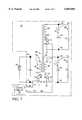
- FIG. 9shows a version of the invention bi-directional dc-to-dc power converter or multiple output multi-directional power converter 110 with supporting circuitry for closed loop bi-directional operation.
- the traditional flyback output rectifiersare replaced by power FET switches 112, 114 (or other bi-directional switches).
- the input bi-directional switch, input power FET 116is driven by the first control signal V1 from the DRV output of PWM 117, a UC 3842.
- the UC 3842is a current mode Pulse Width Modulator Control Integrated Circuit available from the Unitrode company of Merrimack, N.H. 03054, as well as from other suppliers.
- control signalscan be accomplished by many alternative circuit embodiments including those which employ discrete analog and/or digital circuitry, microprocessors, gate arrays, digital signal processors, etc.
- Information about and availability of power FETs for use in the in circuits shownmay be obtained from Motorola's Technical Information Center at Phoenix, Ariz.
- the source of the input bi-directional switch, input power FET 116is connected to ground through current sense resistor 119.
- Integrated Circuit 117is shown powered from an Auxiliary Supply which is customary for reliable starting and control.
- An Auxiliary supplymight initially comprise a separate transformer rectifier set and three terminal regulator to supply VCC, the transformer primary being coupled to a mains supply. In the alternative, the Auxiliary Supply might use a separate battery with continuing power being supplied by the converter after initial power up.
- FIGS. 2-5 and FIGS. 6a-6ceach show the switching characteristics of the first and second control signals V1 and V2.
- FIGS. 2 and 3depict the waveform relationships that can be expected if the duty cycle is 50%.
- FIGS. 4 and 5show the waveforms resulting from a 25% duty cycle.
- FIGS. 2 and 4show the waveforms with a normal load.
- FIGS. 3 and 5show the waveforms with the load reduced to zero.
- Vsis the voltage of the input voltage source applied between the first and second input terminals 12 and 14.
- the waveform for the voltage V4represents the general shape of the voltage waveforms at the drain of the first output bi-directional switch 34 of FIG. 1 and FIG. 7, FIG. 8 and at the drain of the first output bi-directional switches 112 in FIGS. 9 and 10.
- the voltage V5has the same shape as the Voltage V4. Voltage V5 appears at the drains of the second output bi-directional switches 70 of FIGS. 7 and 8, and at the drain of the second output bi-directional switch 114 of FIG. 9.
- waveform for the current Ip in FIGS. 2-5 and FIG. 6a-6crepresents the current into the drain of the input bi-directional switch 116 as it passes through the primary 40 of the coupled inductor 60.
- the waveform Isrepresents the current in the output windings or into the drains of the first and second output bi-directional switches 112, 114.
- the waveform Iorepresents the level of the output current through the load resistors 120a, 120b. Io is the average of the waveform Ic.
- FIGS. 2 and 4 and the circuit of FIG. 9,show that as V1 assumes a high state at time t0, the input bi-directional switch 116 turns on hard and current Ip experiences an initial step rise followed by a ramped rise ending at time t1.
- the initial step in currentis a result of flux or energy expressed in ampere-turns remaining in the core at the conclusion of the previous power cycle.
- energy of some magnitudesupported by the composite sum of the ampere-turns product that depends on the current to the load from the secondary or output windings 123, 124 and the ampere-turns product from magnetizing current, remains in the core at the commencement of any power cycle.
- the bottom waveform in FIG. 2 and FIG. 3represents the capacitor current Ic which is essentially equal to the Is current, except that the average value of the capacitor current is substantially zero.
- the voltage across the loadis constant, so the current through the load is constant.
- the time-varying excursions of the Is currentmust be absorbed by the output voltage source, i.e. capacitors 122a and 122b.
- the capacitorsare designed to have sufficient capacitance to maintain variations in output voltage with a predetermined range, while the area under the Ip curve is proportional to the total input power.
- the current Ipshown entering the dot end of the transformer primary winding, is the result of magnetizing current developing in the primary 40 during each power cycle during the interval t0 to t1.
- Waveform Isjumps to an initial positive value at t1 in response to the input bi-directional switch opening and the output bi-directional switch(s) closing.
- the polarity of the voltage on the output windings 123, 124switches and current continues to enter the dot on the secondaries.
- the magnetizing energy in the core at t1 that is supported by the ampere-turn product in the primaryis transferred to an equivalent ampere-turn product in the output windings 123, 124 as the switches transfer.
- the value of Is ramps down during the interval t1 to t2 as energy in the coreis used to support the voltage across the output voltage source(s) capacitors 122a, 122b.
- Waveforms Ip and Isboth depict currents going to negative values to support the development of negative flux in the core of the transformer.
- the current Isdecreases to a negative value during the interval t1 to t2 because the first and second output switches are on and because the output voltage sources, capacitors 122a and 122b, are charged to the output voltage, and therefore each capacitor drives its respective secondary winding so as to produce negative flux supported by negative ampere-turns as time t2 is reached.
- the negative ampere-turns in the coreresult in the primary winding delivering current from the input winding 40 to the voltage source 12 as the input bi-directional switch 116 is turned on at t2.
- the duty cycle of input power switch 116is described by D
- the duty cycle of the output FET switches 112, 114is described by D'. Whenever the input bi-directional switch 116 is on, the first and second output bi-directional switches 112 and 114 are off. Whenever the input power switch 116 is off, the first and second output bi-directional switches 112 and 114 are on.
- Synchronous rectifier operationis quite different than bi-directional switch operation in the following way. If switches 112 and 114 were to be used as synchronous rectifiers, they would be switched on and off in a manner that would make them emulate rectifiers. Operating as synchronous rectifiers, no current would be permitted to flow from the capacitors 122a, 122b to the output winding(s) 123, 124 during any portion of the power cycle. Conduction in only one direction would be supported or permitted.
- the operation of the multiple output multi-directional power converter of FIG. 9is the same as that of the standard continuous conduction flyback converter utilizing synchronous rectifiers as shown in the waveforms of FIG. 2 and FIG. 4.
- the operationis considerably different from that of a standard flyback in that operation is forced to remain in the continuous conduction mode as shown by the Ip and Is waveforms in FIGS. 3 and 5.
- the discontinuous modewhere flux in the core is allowed to reach zero before t0
- the critical conduction modewhere the flux in the core is allowed to just barely reach zero at t0, are modes that are not allowed.
- the development of negative magnetizing currentresults in the development of negative flux in the core.
- the negative magnetizing fluxis supported by negative ampere-turns in the primary as the output switches 112, 114 are turned off driving the current in the output winding 123, 124 to zero. If a load current had been supported by the output winding, as the output switch was turned off, the ampere-turns product due to the load current would be added to the no-load ampere-turn product, and the composite sum of the products would also be picked up by the input bi-directional switch 116 as an initial positive or negative step in Ip, observable at times t0 and t2 of FIG. 3 and FIG. 5.
- the V2 signalgoes low and turns off the output bi-directional switches 112, 114.
- the flux in the coupled inductor 60causes the polarity of the voltage across the primary winding to reverse due to the flow of current out of the dot at the top of the input winding.
- the result of the switch in polarity an instant before the input bi-directional switch is turned onis that the voltage across the conduction channel is reduced to a near zero value, thus reducing the switching loss in the input bi-directional switch 116 as the current in the primary 40 increases through the conduction channel.
- the reduction in switching lossis obtained by a slight delay between the turn off of the output switches and the turn on of the input switch.
- a similar reduction in switching lossesis enjoyed by the output bi-directional switches as the input bi-directional switch 116 is turned off at t1 and t3.
- the voltage at V4, the drains of the output bi-directional switches 112,124drops to near zero as shown at t1 and t3 thereby reducing switching losses in the respective output bi-directional switches as current flows up from the analog ground "A" into the source of each switch, out of its drain and into the dot at the bottom of each output winding 123, 124.
- the reductions in switching lossesare obtained by a slight delay between the turn off of the input switch and the turn on of the output switches.
- the first control signal V1 from the DRV output of PWM 117drives the primary of pulse transformer 125 through capacitor 126.
- the secondary of transformer 125inverts the drive signal V1 thereby forming the second control signal V2.
- the second control signal V2is then coupled to the gates of output bi-directional switches 112, 114 via delay resistor 128.
- Reactor 130provides a delay in the turn on time of input bi-directional switch 116. As the voltage V1 transitions from the DRV output from a low to a high, a small amount of capacitance between the gate and the source of FET 116 delays the rise in voltage of the gate.
- the reactor 130requires a short time in which to saturate after which it allows drive current from DRV to charge the gate-to-source capacitance of switch 116, after which time the input bi-directional switch 116 turns on.
- the reactoris typically of amorphous magnetic alloy, and such reactors are typically available from Allied Signal in Parsippany, N.J., or from Toshiba and others.
- diode 150provides minimum delay in turning the input bi-directional switch off. It is possible to avoid the need for the delay at turn-on of switch 116 by turning off the output bi-directional switch earlier in the period.
- the performance of the power converter(particularly the cross-regulation between outputs) will not be as good as it is with the second control signal's duty ratio maximized to be as close as practical to the complement of the first control signal. Maximizing the conduction time of the secondary switches improves the cross-regulation and transient response of the outputs. By this same argument, timing methods which do not maximize the conduction times, although perhaps simple and economical, can be used but with some degradation in performance.
- Delay resistor 128 in combination with the gate-to-source capacitance of the output bi-directional switches 112, 114provides a short delay in the turn-on of the switches since the rate of charge is a function of the resistance of resistor 128 and the amplitude of the voltage swing of the secondary of the pulse transformer 125.
- the amplitude of the voltage swingis clamped by diode 134 at a predetermined peak level.
- Resistor 136provides a dc restoring discharge path for coupling capacitor 137.
- the turn-off time of the output switchesis reduced by operation of switching diode 138.
- the delay provided by the reactor 130 in turning the input switch on in combination with the rapid turn off of the secondary switches provided by switching diode 138insures that the output switches will be off before the input switch is on.
- the delay provided by the delay resistor 128is set to exceed the delay through diode 150 at the time the input switch 116 is turned off and the output switches are turned on.
- the longer delay provided by the delay resistor 128 than the delay of the diode 128insures that the output switches 112, 114 will not turn on before the input switch 116 is turned off.
- the output voltage from the output voltage source 122ais shown monitored by reference circuit 140.
- the reference circuitsenses the output voltage via the divider formed by resistors 142 and 144. As the sensed voltage exceeds an internal reference level, the reference circuit 140 provides a current demand at its input C, the current passing through resistor 148 and forward biasing the LED 150 in opto-coupler 152. The greater the sensed voltage excursion, the greater the current demand at the input C of reference circuit 140 and the larger the number of photons that will be produced by LED 150.
- NPN phototransistor 154 in the opto-couplerThe conductance of NPN phototransistor 154 in the opto-coupler is increased by additional photons per unit time.
- the NPN phototransistor 154 in the opto-couplerturns on, pulling down the COMP input to the PWM 117 via resistor 155 thereby causing a reduction in the period of D and increase in the duration of D'.
- a decrease in the sensed voltage at input R to the reference circuitoperates to produce the reverse of the aforementioned occurrences in the characterized feedback sense and control.
- the combination of the components within phantom block 156 and 158therefore provides an embodiment of a means for sensing the output voltage Vo, comparing a portion of the output voltage at the R input of reference amplifier 140 with a precision internal reference voltage, and providing an error voltage into the COMP input of the control IC 117 to increase or decrease duty ratio of the first and second control signals to maintain the output voltage within a predetermined range.
- the integrated circuit 117provides the required clock circuit with a fixed period set by the values of resistor 113 and capacitor 115, and an internal latch which, when set, drives the first control signal to a high state with a high on the DRV output thereby turning on the input bi-directional switch 116.
- the IFB input to the integrated circuit 117receives a current sense voltage at its IFB input from current sense resistor 119 as current passes through the sense resistor.
- the combination of the circuits within phantom blocks 156 and 158provides a control circuit means for providing a clock signal with a fixed period to repeatedly set the output of an internal latch.
- the output of the latchdrives the first control signal V1 high.
- the components within phantom block 156sense the output voltage Vo of the converter.
- Reference amplifier 140compares a portion of the output voltage with a precision internal reference voltage to provide an error voltage.
- the error voltageis conditioned and coupled by the opto-coupler 152 to provide the error voltage to an internal comparator within the integrated circuit 117.
- the current rise in the input windingis converted by the sense resistor 119 into a ramp voltage.
- the internal comparator in IC 117compares the ramp voltage with the error voltage and provides a reset signal to reset the latch to a zero state in response to the ramp voltage exceeding the error voltage.
- the zero set output of the latchdrives the first control signal low turning off the input bi-directional switch 116.
- the internal latchis then set to the one state on receiving the next clock signal.
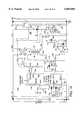
- FIG. 10shows an alternative bi-directional power converter configured to provide operation in the resonant transition conduction mode.
- the object of operation in the resonant transition modeis the virtual elimination of switching losses in the input and output switches by turning the input and output switches 116, 112 on and off at times when there is virtually no voltage across the switch.
- FIGS. 6a-6care three timing diagram charts for each of three load conditions for the bi-directional dc-to-dc power converter of FIG. 10. The period of the first and second control signal is adjusted to provide resonant transitions for both the input and output bi-directional switches 116, 112.
- the V1 and V2 control signalsindicate that the duty ratios are substantially 50% with the total period diminishing with the load current characterized by the peak value of Ip on each of the charts.
- the value of the input voltage Vsis the same in each case.
- the peak amplitude of the voltage at V3, the second terminal 160 of the input winding 40is the same on each of the charts.
- the peak swing of the voltages on the secondary winding V4is the same on each of the three waveforms for V4.
- the circuit of FIG. 10uses the same pulse transformer 125 as shown in FIG. 9 with the same function of providing a second control signal V2 as the complement of control signal V1 from the output 162 of integrated circuit 164.
- a current sense transformer 170is shown having a primary sense winding 172, a secondary sense winding 174 and an output signal winding 176.
- the opto-coupler 152is shown providing the same function as in FIG. 9.
- the collector of NPN phototransistor 154 in the opto-coupleris connected to the Auxiliary Supply.
- the function and operation of the resistor divider pair of resistors 142 and 144is the same as in FIG. 9.
- the valuesare established such that when output voltage Vo is at its proper voltage, the voltage into pin R of integrated reference amplifier 140 is exactly 2.5 volts, or the value of a precision reference. As the output voltage rises above its proper value, integrated circuit 140 detects and amplifies the error and produces a current demand at pin C. Resistor 148 limits the current demand.
- the current demandpasses through the photo diode 150 and the photons produced are coupled to the base of NPN phototransistor 154 to turn it on.
- Resistor divider 182, 184couples a small rise in voltage into the VFB input 186 of the integrated circuit 190, a UC 3852 Power Factor Correction Circuit.
- the UC 3852is a pulse width modulator adapted for critical conduction flyback operation, also available from the Unitrode Corporation mentioned above.
- control signal V1transitions to a positive value at t0
- input bi-directional switch 116turns on.
- the conduction channel of switch 116connects the second terminal of the input winding 40 of transformer 60 to return 14.
- the output bi-directional switchis open. Current begins to ramp up in the primary as indicated by the waveform Ip at t0. The rate of rise is limited by the self-inductance of the primary or input winding 40 and the applied input voltage Vs.
- the resistor divider formed by resistors 188 and 189provide a positive bias voltage into the ISNS input 191 of integrated circuit 190.
- the input current Ippasses into the dot and through the first sense winding 172 of current sense transformer 170.
- the second sense winding 174 branchis open during this interval.
- the lower half of signal winding 176is terminated by scaling resistor 189 via forward biased signal diode 192.
- Negative ramp voltage Vadevelops across this lower half of signal winding 176 in response to the current Ip increasing in first sense winding 172.
- the current in the lower half of winding 176is inversely proportional to the ratio of turns in the first sense winding 172 to turns in the lower half of the signal winding 176.
- the output current Ispasses into the dot at the bottom of the second sense winding 172 of current sense transformer 170.
- the first sense winding 174 branchis open during this interval, but the upper half of signal winding 176 is terminated by scaling resistor 194 via forward biased signal diode 193.
- a positive ramp voltage Vbdevelops on the upper half of the signal winding 170 during the interval from t1 to t2.
- resistor 188, 189are calculated to establish a quiescent operating voltage at the ISNS input 191 slightly above zero volts such that when current in the first or second sense windings goes to zero, the voltage into the ISNS input 191 crosses from a negative signal value to a few millivolts above zero volts. This operation point is important because a zero volt crossing resets integrated circuit 190, the UC 3852 starts the next power cycle at a point where there is virtually no current in the input bi-directional switch.
- the UC 3852is a controlled on-time PWM that has a clock circuit or timer with an on-time that can be modulated by an external voltage.
- the clock periodis programmed by external resistor 194 from the ISET terminal to GND.
- a timing capacitor 195 connected from the RAMP terminal to the GND terminal of the UC 3852sets the on-time in conjunction with the voltage at the COMP terminal. Typical values for the timing capacitor range from 100 pF to 1 nF.
- first control signal V1goes low turning off the input bi-directional switch 116 via speed-up diode 150.
- V2goes high turning on the output bi-directional switch 112 with the small delay provided by resistor 128 and the gate-to-source capacitance of output bi-directional switch 112.
- the turn off of switch 116is very fast and can be substantially lossless.
- the turn off of switch 116 and the interruption of current into the dot on winding 40induces a polarity change on the secondary winding driving the voltage at V4, the drain of switch 112, to a level one diode drop below the analog ground "A" where it is clamped by the body diode of switch 112 until the gate voltage of switch 112 rises turning the switch 112 on.
- Switch 112thereby turns on at t1 with virtually no voltage across it thereby avoiding switching losses at turn on.
- the period of the V2 termis sufficient to allow the secondary current Is and the current in the output signal winding IT2S through register 189 to go to zero or to a valve sufficiently low to allow the voltage at Vc into the ISNS input 191 to rise a few millivolts positive above ground as shown by the waveform Vc on FIGS. 6a-6c.
- the second control signal V2then goes low turning off the output bi-directional switch 112 at a time when the current passing through the switch has dropped through zero and has gone slightly negative as a result of voltage applied by the output voltage source capacitor 122a. At this time output bi-directional switch 112 is turned off very quickly, resulting in an essentially lossless transition.
- the slight amount of negative current that is permitted to develop in the output windingis adjusted by the control process to be sufficient to cause the polarity of the voltage on the primary winding to reverse as current in the secondary is interrupted by the turn off of the output bi-directional switch 112. Interruption of current in the secondary is adjusted by the delays and operating point to switch the polarity of the voltage across the primary, driving the voltage on the drain of input bi-directional switch 116 negative until it is clamped by the body diode of input bi-directional switch 116 slightly before the first control signal overcomes the delay resulting from reactor 130 and the gate-to-source capacitance of switch 116, turning on switch 116 at t2. The turn on of switch 116 occurs at a time where there is virtually no current passing through the switch 116 and there is no voltage across the switch 116, thereby again resulting in very low switching losses.
- the circuit of FIG. 10is therefore not only a bi-directional flyback converter such as the converter of FIG. 9, but is also essentially a critical conduction variable frequency flyback utilizing a modified synchronously rectified secondary.
- the turn-off of the synchronous output FET, the output bi-directional switch 112is delayed past the zero current point in order to build up a small amount of reverse energy in the core of the coupled inductor 60, at which time the output bi-directional switch 112, is turned off.
- the reverse energy in the corethen causes a lossless transition of the input FET, input bi-directional switch 116, at which time its gate drive is applied. Current then ramps up in the primary, the input winding 40 through the input bi-directional switch 116 in a normal manner until terminated by the control signal V1 driving the gate low.
- FIG. 11shows a functional embodiment of a resonant transition control means for sensing the coupled inductor input and output winding currents and the output voltage and for adjusting the clock frequency to provide operation in a resonant transition mode and to adjust the output voltage to a predetermined level.
- the resonant transition control meansprovides a reduction in frequency in response to an increase in load and an increase in frequency in response to a reduction in load. Switching by the input bi-directional switch 112 of the input winding occurs at near zero voltage at t0 and t2 as a result of reverse current into the output winding from the output voltage source.
- Lossesare minimized at the turn off of the input bi-directional switch 116 at t1 by sharpening the fall of the voltage on the gate by use of speed-up diode 150.
- the components within phantom block 156sense the output voltage Vo of the converter.
- Reference amplifier 140compares a portion of the output voltage with a precision internal reference voltage to provide an error voltage.
- the error voltageis conditioned and coupled by the opto-coupler 152 to provide the error voltage to an internal error signal amplifier 218 within the integrated circuit 190.
- FIG. 11is shown as the sense voltage Vc has risen to zero volts and the input threshold amplifier 208 has switched its output from a low to a high, setting the R-S flip-flop (FF) 210 output Q to the one or high state.
- the Q' outputgoes low turning off the NPN transistor 212, thereby allowing the ramp generator 214 to provides a ramp to the non-inverting input of comparator 216.
- the comparatorreceives an error signal from an error signal amplifier 218, at the comparator's inverting input. The error signal rises or falls depending on whether the output voltage is below or above the flyback output voltage Vo operating design range.
- the comparator 216drives the reset terminal of the R-S FF 210 via OR gate 220 to reset the FF at t1.
- the Q' output of the R-S FFis the second control signal V2 which when high, turns on the output bi-directional switch 112, which allows the current in the secondary to ramp down and the voltage Vc to rise to zero.
- the Q output of FF 210goes low to turn off the input bi-directional switch 116.
- the Q' outputgoes high and turns on the NPN transistor 212 and discharges the capacitor 195. The capacitor remains discharged until the FF is once again set by the voltage Vc rising through zero. The overall period will therefore vary to accommodate the rise and fall of the output voltage Vo.
- a low first control signalresults in a high second control signal, V2, via transformer 125.
- a high V2 termturns on the output bi-directional switch 112 allowing the current in the secondary to ramp downward.
- the current in the output windingcontinues to ramp downward until voltage Vc crosses zero volts at the input of the input threshold amplifier 208. As the current in the output winding ramps downward, the voltage Vc ramps upward toward zero.
- An increase in the error signal into the error signal amplifier 218reduces the error signal out of error signal amplifier 218 thereby reducing the time required for the internal ramp generator to reset the R-S FF, thereby also reducing the on time of the first control signal.
- a reduction of the error signal into the error amplifier 218produces the reverse result.
- the multiple output multi-directional power convertersimplifies battery backup operation. If a battery of equal voltage to output 1 were placed in parallel with output 1 and the input power source were removed, output 2 would continue to supply power to its load by energy flowing into output 1 from the battery. In the multiple output multi-directional power converter, it is possible to back up a plurality of outputs by placing a voltage source across any output.
- variable frequency single-output resonant mode converter embodiment of the inventionThe following advantages are provided by the variable frequency single-output resonant mode converter embodiment of the invention.
- variable frequency single-output resonant mode converterreduces switching losses particularly on bi-directional switch turn on which would allow operation at higher frequencies.
- variable frequency circuitdoes not exhibit frequency run away at no load as do some variable frequency critical conduction flyback regulators.
- FIG. 9is an example of a quite useful flyback topology in which this invention is applied with all of the advantages described earlier herein.
Landscapes
- Engineering & Computer Science (AREA)
- Power Engineering (AREA)
- Dc-Dc Converters (AREA)
Abstract
Description
Claims (17)
Priority Applications (2)
| Application Number | Priority Date | Filing Date | Title |
|---|---|---|---|
| US09/359,499US6069804A (en) | 1998-07-28 | 1999-07-23 | Bi-directional dc-to-dc power converter |
| PCT/US1999/016951WO2000007287A2 (en) | 1998-07-28 | 1999-07-27 | A bi-directional dc-to-dc power converter |
Applications Claiming Priority (2)
| Application Number | Priority Date | Filing Date | Title |
|---|---|---|---|
| US9444898P | 1998-07-28 | 1998-07-28 | |
| US09/359,499US6069804A (en) | 1998-07-28 | 1999-07-23 | Bi-directional dc-to-dc power converter |
Publications (1)
| Publication Number | Publication Date |
|---|---|
| US6069804Atrue US6069804A (en) | 2000-05-30 |
Family
ID=26788893
Family Applications (1)
| Application Number | Title | Priority Date | Filing Date |
|---|---|---|---|
| US09/359,499Expired - LifetimeUS6069804A (en) | 1998-07-28 | 1999-07-23 | Bi-directional dc-to-dc power converter |
Country Status (2)
| Country | Link |
|---|---|
| US (1) | US6069804A (en) |
| WO (1) | WO2000007287A2 (en) |
Cited By (102)
| Publication number | Priority date | Publication date | Assignee | Title |
|---|---|---|---|---|
| US6243277B1 (en)* | 2000-05-05 | 2001-06-05 | Rockwell Collins, Inc. | Bi-directional dc to dc converter for energy storage applications |
| US6268666B1 (en)* | 1999-02-25 | 2001-07-31 | Southwest Research Institute | Bi-directional power conversion apparatus for combination of energy sources |
| US6285568B1 (en)* | 1997-12-23 | 2001-09-04 | Sextant Avionique | Process for controlling a DC/DC converter with inductive storage and including an energetically neutral phase |
| US6324077B1 (en)* | 2001-04-19 | 2001-11-27 | Martek Power, Inc. | Switch mode power supply |
| US6330169B2 (en)* | 2000-02-25 | 2001-12-11 | Condor D.C. Power Supplies Inc. | Converter output regulation via channel resistance modulation of synchronous rectifiers |
| US6344985B1 (en) | 2000-12-05 | 2002-02-05 | Heart Transverter S.A. | Multiple port bi-directional power converter |
| US6366060B1 (en)* | 2000-08-10 | 2002-04-02 | Delphi Technologies, Inc. | Mosfet control circuit for dual winding alternator |
| US6366480B2 (en)* | 2000-03-03 | 2002-04-02 | Murata Manufacturing Co. | Switching power supply apparatus |
| US6373726B1 (en)* | 1999-01-28 | 2002-04-16 | Power-One A.G. | Flyback converter with transistorized rectifier controlled by primary side control logic |
| WO2002069675A1 (en)* | 2001-02-26 | 2002-09-06 | Pelikon Ltd | Electronic circuits |
| WO2002045249A3 (en)* | 2000-12-01 | 2002-09-19 | Siemens Ag | Circuit arrangement for dc/dc converters with low output voltage |
| US20030058661A1 (en)* | 2001-09-26 | 2003-03-27 | Smidt Pieter Jan Mark | Split topology power supply architecture |
| US6570268B1 (en) | 2000-11-20 | 2003-05-27 | Artesyn Technologies, Inc. | Synchronous rectifier drive circuit and power supply including same |
| US6594161B2 (en) | 2000-11-11 | 2003-07-15 | Minebea Co., Ltd. | Power converter having independent primary and secondary switches |
| US6606257B2 (en)* | 2001-11-05 | 2003-08-12 | Koninklijke Philips Electronics N.V. | Independent regulation of multiple outputs in a soft-switching multiple-output flyback converter |
| WO2003094331A1 (en)* | 2002-05-03 | 2003-11-13 | Minebea Co. Ltd. | Power converter |
| US20030235059A1 (en)* | 2000-11-20 | 2003-12-25 | Marty Perry | Synchronous rectifier drive circuit and power supply including same |
| US6690585B2 (en) | 2001-08-29 | 2004-02-10 | Oqo, Inc. | Bi-directional DC power conversion system |
| WO2004015850A1 (en)* | 2002-08-12 | 2004-02-19 | Siemens Ag Österreich | Dc-to-dc converter |
| WO2003088460A3 (en)* | 2002-04-12 | 2004-02-26 | Delta Energy Systems Switzerla | Soft switching high efficiency flyback converter |
| US6713894B1 (en)* | 1997-12-11 | 2004-03-30 | Bayerische Motoren Werke Aktiengesellschaft | Device for supplying electricity to a motor vehicle |
| US20040062066A1 (en)* | 2000-12-22 | 2004-04-01 | Crocker Timothy Richard | Switched mode circuit topologies |
| US20040062061A1 (en)* | 2002-09-26 | 2004-04-01 | Koninklijke Philips Electronics N. V. | Regulation of bi-directional flyback converter |
| US6717388B2 (en)* | 2000-10-27 | 2004-04-06 | Koninklijke Philips Electronics N.V. | Bidirectional converter with input voltage control by a primary switch and output voltage regulation by a secondary switch |
| US20040075600A1 (en)* | 2002-10-16 | 2004-04-22 | Perkinelmer Inc. A Massachusetts Corporation | Data processor controlled DC to DC converter system and method of operation |
| US20040239299A1 (en)* | 2002-08-08 | 2004-12-02 | Vlt, Inc., A California Corporation | Buck-boost DC-DC switching power conversion |
| EP1499004A1 (en)* | 2003-07-17 | 2005-01-19 | Puls Elektronische Stromversorgungs GmbH | Method for controlling a synchronous rectifier and synchronous rectifier controller |
| US20050231984A1 (en)* | 2004-04-19 | 2005-10-20 | Po-Wen Wang | Switching power converter |
| US20050248964A1 (en)* | 2004-05-10 | 2005-11-10 | Semiconductor Components Industries, Llc. | Power supply controller and method therefor |
| US20050264271A1 (en)* | 2004-05-11 | 2005-12-01 | The Hong Kong University Of Science And Technology | Single inductor multiple-input multiple-output switching converter and method of use |
| US20050270813A1 (en)* | 2004-06-04 | 2005-12-08 | Wanfeng Zhang | Parallel current mode control |
| US20060002155A1 (en)* | 2003-06-30 | 2006-01-05 | Anatoly Shteynberg | System and method for input current shaping in a power converter |
| US20060006850A1 (en)* | 2003-08-05 | 2006-01-12 | Manabu Inoue | Direct-current power supply and battery-powered electronic apparatus and equipped with the power supply |
| US20060017329A1 (en)* | 2004-07-21 | 2006-01-26 | Pierre Brault | Inverter and bi-directional converter |
| EP1626490A1 (en)* | 2004-08-11 | 2006-02-15 | SMK Corporation | A synchronous rectifying switching power source circuit |
| US20060039172A1 (en)* | 2004-08-23 | 2006-02-23 | International Rectifier Corporation | Circuit to improve capacitor hold-up time in a converter circuit |
| US20060061337A1 (en)* | 2004-09-21 | 2006-03-23 | Jung-Won Kim | Power factor correction circuit |
| US20060197514A1 (en)* | 2003-06-19 | 2006-09-07 | Koninklijke Philips Electronics N.V. | Switch mode power circuit |
| US7113413B1 (en)* | 2004-05-12 | 2006-09-26 | Fairchild Semiconductor Corporation | Control circuit with tracking turn on/off delay for a single-ended forward converter with synchronous rectification |
| US20060238029A1 (en)* | 2005-04-22 | 2006-10-26 | Texas Instruments, Inc. | DC/DC power converter |
| US20060244430A1 (en)* | 2005-04-27 | 2006-11-02 | Nobuo Hirabayashi | DC/DC converter |
| US20070230222A1 (en)* | 2006-03-31 | 2007-10-04 | Drabing Richard B | Power circuitry for high-frequency applications |
| US20080116872A1 (en)* | 2006-11-22 | 2008-05-22 | Nec Electronics Corporation | DC-DC converter |
| US20080130334A1 (en)* | 2003-06-19 | 2008-06-05 | Koninlijke Philips Electronics N.V. | Determining Reflected Power |
| US20080238201A1 (en)* | 2007-03-29 | 2008-10-02 | Fred Oliver | Aircraft Power System and Apparatus for Supplying Power to an Aircraft Electrical System |
| US7433211B1 (en) | 2003-06-30 | 2008-10-07 | Iwatt Inc. | System and method for input current shaping in a power converter |
| US20080266910A1 (en)* | 2007-04-30 | 2008-10-30 | Samsung Electronics Co., Ltd. | Power supply apparatus having multiple outputs |
| US20080303981A1 (en)* | 2004-06-11 | 2008-12-11 | Pelikon Limited | Electroluminescent Displays |
| US20090109711A1 (en)* | 2007-10-26 | 2009-04-30 | Ta-Ching Hsu | Three-pin integrated synchronous rectifier and a flyback synchronous rectifying circuit |
| US7558083B2 (en) | 1997-01-24 | 2009-07-07 | Synqor, Inc. | High efficiency power converter |
| US7564702B2 (en) | 1997-01-24 | 2009-07-21 | Synqor, Inc. | High efficiency power converter |
| US20090237053A1 (en)* | 2008-03-24 | 2009-09-24 | Active-Semi International, Inc. | High efficiency voltage regulator with auto power-save mode |
| US7738271B1 (en) | 2007-06-08 | 2010-06-15 | Science Applications International Corporation | Controlled resonant charge transfer device |
| US20100148587A1 (en)* | 2008-12-17 | 2010-06-17 | Alireza Khaligh | Multiple-input dc-dc converter |
| US20110235368A1 (en)* | 2010-03-29 | 2011-09-29 | Smartsynch, Inc. | System and method for conversion of high voltage ac to low voltage dc using input voltage gating |
| US20120119574A1 (en)* | 2010-11-15 | 2012-05-17 | Mitsubishi Electric Corporation | Power supply device for vehicle |
| US20120181873A1 (en)* | 2009-07-20 | 2012-07-19 | Robert Bosch Gmbh | Hybrid Battery System |
| US20120250360A1 (en)* | 2011-04-01 | 2012-10-04 | Power Integrations, Inc. | Llc controller with programmable fractional burst frequency |
| US8498172B1 (en) | 2010-08-31 | 2013-07-30 | Western Digital Technologies, Inc. | Data storage device evaluating frequency range of supply voltage to detect power failure |
| US20130194846A1 (en)* | 2012-01-31 | 2013-08-01 | Green Charge Networks | Universal single-stage power converter |
| US20130194847A1 (en)* | 2012-01-31 | 2013-08-01 | The Prosser Group Llc Dba Green Charge Networks | Universal power conversion methods and systems |
| US20140003096A1 (en)* | 2012-07-02 | 2014-01-02 | Silergy Semiconductor Technology (Hangzhou) Ltd | Synchronous rectification control circuit and power supply thereof |
| US20140098578A1 (en)* | 2012-10-05 | 2014-04-10 | Nxp B.V. | Switched mode power supplies |
| US8780586B2 (en) | 2007-11-16 | 2014-07-15 | Itron, Inc. | Devices and methods for converting alternating current (AC) power to direct current (DC) power |
| US20140354040A1 (en)* | 2011-11-22 | 2014-12-04 | Continental Automotive Gmbh | Vehicle Electrical System And Method For Operating A Vehicle Electrical System |
| US8953343B2 (en) | 2007-04-30 | 2015-02-10 | Samsung Electronics Co., Ltd. | Power supply apparatus having multiple outputs |
| US8953342B2 (en) | 2012-04-12 | 2015-02-10 | On-Bright Electronics (Shanghai) Co., Ltd. | Systems and methods for regulating power conversion systems with output detection and synchronized rectifying mechanisms |
| TWI473411B (en)* | 2012-07-30 | 2015-02-11 | Delta Electronics Inc | Synchronous rectifying apparatus and controlling method thereof |
| US20150049519A1 (en)* | 2012-03-20 | 2015-02-19 | Indiana University Research & Technology Corporation | Single Switch Infinite-Level Power Inverters |
| US8964420B2 (en) | 2011-12-13 | 2015-02-24 | Apple Inc. | Zero voltage switching in flyback converters with variable input voltages |
| US8975957B1 (en) | 2013-08-21 | 2015-03-10 | On-Bright Electronics (Shanghai) Co., Ltd. | Amplification systems and methods with one or more channels |
| US20150311865A1 (en)* | 2013-01-14 | 2015-10-29 | Cognipower, Llc | Flyback Amplifier with Direct Feedback |
| US20160020703A1 (en)* | 2014-07-17 | 2016-01-21 | Infineon Technologies Austria Ag | Synchronous rectification for flyback converter |
| US9315166B2 (en) | 2013-07-12 | 2016-04-19 | Fca Us Llc | Techniques for synchronous rectification control of DC-DC converters in electrified vehicles |
| US9413246B2 (en) | 2012-04-12 | 2016-08-09 | On-Bright Electronics (Shanghai) Co., Ltd. | Systems and methods for regulating power conversion systems with output detection and synchronized rectifying mechanisms |
| US9595876B2 (en) | 2015-02-11 | 2017-03-14 | Schneider Electric It Corporation | DC-DC converter |
| US9595874B2 (en) | 2012-04-12 | 2017-03-14 | On-Bright Electronics (Shanghai) Co., Ltd. | Systems and methods for regulating power conversion systems with output detection and synchronized rectifying mechanisms |
| US9685919B2 (en) | 2013-08-21 | 2017-06-20 | On-Bright Electronics (Shanghai) Co., Ltd. | Amplification systems and methods with output regulation |
| US9787198B1 (en) | 2016-05-23 | 2017-10-10 | On-Bright Electronics (Shanghai) Co., Ltd. | Systems and methods with prediction mechanisms for synchronization rectifier controllers |
| US9853542B2 (en)* | 2013-02-28 | 2017-12-26 | Bcd Semiconductor Manufacturing Limited | Constant-voltage and constant-current buck converter and control circuit |
| US9853551B2 (en)* | 2016-05-02 | 2017-12-26 | Toyota Jidosha Kabushiki Kaisha | Isolated DC-DC power conversion circuit |
| US9859803B2 (en)* | 2013-04-23 | 2018-01-02 | Analog Devices Global | Transformer-based isolated bi-directional DC-DC power converter, and method and controller for using same |
| US9887643B2 (en)* | 2013-09-20 | 2018-02-06 | Indiana University Research And Technology Corporation | Bidirectional electrical signal converter |
| US9939384B2 (en) | 2013-09-30 | 2018-04-10 | Honeywell International Inc. | Low-powered system for driving a fuel control mechanism |
| US9991811B1 (en)* | 2016-12-06 | 2018-06-05 | Delta Electronics (Shanghai) Co., Ltd. | Control method and control apparatus for flyback circuit |
| US10033182B2 (en) | 2013-07-22 | 2018-07-24 | Indiana University Research And Technology Corporation | Bidirectional electrical signal converter |
| US10050519B2 (en) | 2016-12-02 | 2018-08-14 | Vlt, Inc. | Control of buck-boost power converter with input voltage tracking |
| US10148189B2 (en) | 2017-02-24 | 2018-12-04 | On-Bright Electronics (Shanghai) Co., Ltd. | Systems and methods with timing control for synchronization rectifier controllers |
| US10199950B1 (en) | 2013-07-02 | 2019-02-05 | Vlt, Inc. | Power distribution architecture with series-connected bus converter |
| US10320300B2 (en) | 2016-07-29 | 2019-06-11 | On-Bright Electronics (Shanghai) Co., Ltd. | Systems and methods for reducing switching loss in power conversion systems |
| US20190326825A1 (en)* | 2018-04-19 | 2019-10-24 | Xi'an Jiaotong University | Miniature fast charging and discharging circuit |
| US10622903B2 (en) | 2012-04-12 | 2020-04-14 | On-Bright Electronics (Shanghai) Co., Ltd. | Systems and methods for regulating power conversion systems with output detection and synchronized rectifying mechanisms |
| KR20210075146A (en)* | 2018-10-18 | 2021-06-22 | 오울스톤 아이엔씨. | waveform generator |
| WO2023156871A1 (en)* | 2022-02-16 | 2023-08-24 | 3M Innovative Properties Company | Power supply system, article of personal protective equipment, and method of improving power efficiency of power supply system |
| CN116711218A (en)* | 2020-11-20 | 2023-09-05 | Ams-欧司朗国际有限公司 | Driver circuit and method of providing pulses |
| US11757366B2 (en) | 2020-05-29 | 2023-09-12 | On-Bright Electronics (Shanghai) Co., Ltd. | Systems and methods for synchronous rectification of power supply systems |
| US11764697B2 (en) | 2020-01-20 | 2023-09-19 | On-Bright Electronics (Shanghai) Co., Ltd. | Systems and methods for controlling synchronous rectification |
| US20230318471A1 (en)* | 2022-03-30 | 2023-10-05 | Infineon Technologies Austria Ag | Circuit for bi-directional converter, bi-directional converter and operation method thereof |
| US11962275B2 (en) | 2011-09-06 | 2024-04-16 | On-Bright Electronics (Shanghai) Co., Ltd. | Amplification systems and methods with distortion reductions |
| US12047007B2 (en) | 2021-03-11 | 2024-07-23 | On-Bright Electronics (Shanghai) Co., Ltd. | Systems and methods for controlling gate voltage increase on primary side to reduce voltage spike on secondary side of switching power supplies |
| US12095379B2 (en) | 2021-07-07 | 2024-09-17 | On-Bright Electronics (Shanghai) Co., Ltd. | Systems and methods for controlling synchronous rectification with variable voltage regulation |
| JP2024539969A (en)* | 2021-10-25 | 2024-10-31 | ローベルト ボツシユ ゲゼルシヤフト ミツト ベシユレンクテル ハフツング | Control method and apparatus for measuring impedance spectrum of a battery |
Families Citing this family (1)
| Publication number | Priority date | Publication date | Assignee | Title |
|---|---|---|---|---|
| EP2429071A4 (en)* | 2010-11-01 | 2013-10-23 | Arkady Anatolievich Stepanov | Autonomous electrical power supply source with a recharging function using one rechargeable battery |
Citations (18)
| Publication number | Priority date | Publication date | Assignee | Title |
|---|---|---|---|---|
| US3569818A (en)* | 1969-07-22 | 1971-03-09 | Hughes Aircraft Co | Multiple output dc voltage regulator |
| US3986097A (en)* | 1975-06-30 | 1976-10-12 | Bell Telephone Laboratories, Incorporated | Bilateral direct current converters |
| US4491835A (en)* | 1982-03-24 | 1985-01-01 | Allied Corporation | Raster and stroke writing deflection amplifier arrangement |
| US4716514A (en)* | 1984-12-13 | 1987-12-29 | Unitrode Corporation | Synchronous power rectifier |
| US4736151A (en)* | 1986-12-23 | 1988-04-05 | Sundstrand Corporation | Bi-directional buck/boost DC/DC converter |
| US4853837A (en)* | 1988-08-08 | 1989-08-01 | Zdzislaw Gulczynski | Synchronous switching power supply with flyback converter |
| US5221887A (en)* | 1988-08-08 | 1993-06-22 | Zdzislaw Gulczynski | Synchronous switching power supply comprising boost or flyback converter |
| US5237606A (en)* | 1991-05-01 | 1993-08-17 | Charles Industries, Ltd. | Enhanced synchronous rectifier |
| US5303138A (en)* | 1993-04-29 | 1994-04-12 | At&T Bell Laboratories | Low loss synchronous rectifier for application to clamped-mode power converters |
| US5402329A (en)* | 1992-12-09 | 1995-03-28 | Ernest H. Wittenbreder, Jr. | Zero voltage switching pulse width modulated power converters |
| US5552695A (en)* | 1994-03-22 | 1996-09-03 | Linear Technology Corporation | Synchronously rectified buck-flyback DC to DC power converter |
| US5594629A (en)* | 1994-06-20 | 1997-01-14 | General Electric Company | High-frequency switching circuits operable in a natural zero-voltage switching mode |
| US5625541A (en)* | 1993-04-29 | 1997-04-29 | Lucent Technologies Inc. | Low loss synchronous rectifier for application to clamped-mode power converters |
| US5636116A (en)* | 1993-07-14 | 1997-06-03 | Melcher Ag | Synchronous rectifier impervious to reverse feed |
| US5663874A (en)* | 1995-09-19 | 1997-09-02 | Micro Linear Corporation | Multiple output flyback DC-to-DC converter with synchronous rectification and constant on-time current mode control |
| US5828558A (en)* | 1998-02-11 | 1998-10-27 | Powerdsine, Ltd. | PWN controller use with open loop flyback type DC to AC converter |
| US5959241A (en)* | 1998-04-30 | 1999-09-28 | Digital Equipment Corporation | Scanning force microscope thermal microprobe |
| EP1174265A2 (en)* | 1996-01-29 | 2002-01-23 | Seiko Epson Corporation | Ink-jet recording head |
Family Cites Families (1)
| Publication number | Priority date | Publication date | Assignee | Title |
|---|---|---|---|---|
| JPH01174265A (en)* | 1987-12-25 | 1989-07-10 | Mitsubishi Electric Corp | power converter |
- 1999
- 1999-07-23USUS09/359,499patent/US6069804A/ennot_activeExpired - Lifetime
- 1999-07-27WOPCT/US1999/016951patent/WO2000007287A2/enactiveApplication Filing
Patent Citations (19)
| Publication number | Priority date | Publication date | Assignee | Title |
|---|---|---|---|---|
| US3569818A (en)* | 1969-07-22 | 1971-03-09 | Hughes Aircraft Co | Multiple output dc voltage regulator |
| US3986097A (en)* | 1975-06-30 | 1976-10-12 | Bell Telephone Laboratories, Incorporated | Bilateral direct current converters |
| US4491835A (en)* | 1982-03-24 | 1985-01-01 | Allied Corporation | Raster and stroke writing deflection amplifier arrangement |
| US4716514A (en)* | 1984-12-13 | 1987-12-29 | Unitrode Corporation | Synchronous power rectifier |
| US4736151A (en)* | 1986-12-23 | 1988-04-05 | Sundstrand Corporation | Bi-directional buck/boost DC/DC converter |
| US4853837A (en)* | 1988-08-08 | 1989-08-01 | Zdzislaw Gulczynski | Synchronous switching power supply with flyback converter |
| US5221887A (en)* | 1988-08-08 | 1993-06-22 | Zdzislaw Gulczynski | Synchronous switching power supply comprising boost or flyback converter |
| US5237606A (en)* | 1991-05-01 | 1993-08-17 | Charles Industries, Ltd. | Enhanced synchronous rectifier |
| US5402329A (en)* | 1992-12-09 | 1995-03-28 | Ernest H. Wittenbreder, Jr. | Zero voltage switching pulse width modulated power converters |
| US5303138A (en)* | 1993-04-29 | 1994-04-12 | At&T Bell Laboratories | Low loss synchronous rectifier for application to clamped-mode power converters |
| US5528482A (en)* | 1993-04-29 | 1996-06-18 | At&T Corp. | Low loss synchronous rectifier for application to clamped-mode power converters |
| US5625541A (en)* | 1993-04-29 | 1997-04-29 | Lucent Technologies Inc. | Low loss synchronous rectifier for application to clamped-mode power converters |
| US5636116A (en)* | 1993-07-14 | 1997-06-03 | Melcher Ag | Synchronous rectifier impervious to reverse feed |
| US5552695A (en)* | 1994-03-22 | 1996-09-03 | Linear Technology Corporation | Synchronously rectified buck-flyback DC to DC power converter |
| US5594629A (en)* | 1994-06-20 | 1997-01-14 | General Electric Company | High-frequency switching circuits operable in a natural zero-voltage switching mode |
| US5663874A (en)* | 1995-09-19 | 1997-09-02 | Micro Linear Corporation | Multiple output flyback DC-to-DC converter with synchronous rectification and constant on-time current mode control |
| EP1174265A2 (en)* | 1996-01-29 | 2002-01-23 | Seiko Epson Corporation | Ink-jet recording head |
| US5828558A (en)* | 1998-02-11 | 1998-10-27 | Powerdsine, Ltd. | PWN controller use with open loop flyback type DC to AC converter |
| US5959241A (en)* | 1998-04-30 | 1999-09-28 | Digital Equipment Corporation | Scanning force microscope thermal microprobe |
Non-Patent Citations (2)
| Title |
|---|
| Article, by C. P. Henze, H. C. Martin and D. W. Parsley Zero Voltage Switching in High Frequency Power Converters using Pulse Width Modulation APEC Record, Feb. 1 5, 1988, pp. 33 41; Published Sep. 1988, by IEEE as IEEE Publication, CH2504 9/88/0000 $1.00 pp. 33 through 40.* |
| Article, by C. P. Henze, H. C. Martin and D. W. Parsley Zero-Voltage Switching in High Frequency Power Converters using Pulse Width Modulation APEC Record, Feb. 1-5, 1988, pp. 33-41; Published Sep. 1988, by IEEE as IEEE Publication, CH2504-9/88/0000 $1.00 pp. 33 through 40. |
Cited By (187)
| Publication number | Priority date | Publication date | Assignee | Title |
|---|---|---|---|---|
| US7564702B2 (en) | 1997-01-24 | 2009-07-21 | Synqor, Inc. | High efficiency power converter |
| US7558083B2 (en) | 1997-01-24 | 2009-07-07 | Synqor, Inc. | High efficiency power converter |
| US8023290B2 (en) | 1997-01-24 | 2011-09-20 | Synqor, Inc. | High efficiency power converter |
| US8493751B2 (en) | 1997-01-24 | 2013-07-23 | Synqor, Inc. | High efficiency power converter |
| US9143042B2 (en) | 1997-01-24 | 2015-09-22 | Synqor, Inc. | High efficiency power converter |
| US6713894B1 (en)* | 1997-12-11 | 2004-03-30 | Bayerische Motoren Werke Aktiengesellschaft | Device for supplying electricity to a motor vehicle |
| US6285568B1 (en)* | 1997-12-23 | 2001-09-04 | Sextant Avionique | Process for controlling a DC/DC converter with inductive storage and including an energetically neutral phase |
| US6373726B1 (en)* | 1999-01-28 | 2002-04-16 | Power-One A.G. | Flyback converter with transistorized rectifier controlled by primary side control logic |
| US6268666B1 (en)* | 1999-02-25 | 2001-07-31 | Southwest Research Institute | Bi-directional power conversion apparatus for combination of energy sources |
| US6330169B2 (en)* | 2000-02-25 | 2001-12-11 | Condor D.C. Power Supplies Inc. | Converter output regulation via channel resistance modulation of synchronous rectifiers |
| US6366480B2 (en)* | 2000-03-03 | 2002-04-02 | Murata Manufacturing Co. | Switching power supply apparatus |
| US6243277B1 (en)* | 2000-05-05 | 2001-06-05 | Rockwell Collins, Inc. | Bi-directional dc to dc converter for energy storage applications |
| US6366060B1 (en)* | 2000-08-10 | 2002-04-02 | Delphi Technologies, Inc. | Mosfet control circuit for dual winding alternator |
| US6717388B2 (en)* | 2000-10-27 | 2004-04-06 | Koninklijke Philips Electronics N.V. | Bidirectional converter with input voltage control by a primary switch and output voltage regulation by a secondary switch |
| US6594161B2 (en) | 2000-11-11 | 2003-07-15 | Minebea Co., Ltd. | Power converter having independent primary and secondary switches |
| US6570268B1 (en) | 2000-11-20 | 2003-05-27 | Artesyn Technologies, Inc. | Synchronous rectifier drive circuit and power supply including same |
| US20030235059A1 (en)* | 2000-11-20 | 2003-12-25 | Marty Perry | Synchronous rectifier drive circuit and power supply including same |
| US6831847B2 (en) | 2000-11-20 | 2004-12-14 | Artesyn Technologies, Inc. | Synchronous rectifier drive circuit and power supply including same |
| WO2002045249A3 (en)* | 2000-12-01 | 2002-09-19 | Siemens Ag | Circuit arrangement for dc/dc converters with low output voltage |
| US6344985B1 (en) | 2000-12-05 | 2002-02-05 | Heart Transverter S.A. | Multiple port bi-directional power converter |
| US20040062066A1 (en)* | 2000-12-22 | 2004-04-01 | Crocker Timothy Richard | Switched mode circuit topologies |
| US7102299B2 (en) | 2001-02-26 | 2006-09-05 | Pelikon Limited | Electronic circuits |
| WO2002069675A1 (en)* | 2001-02-26 | 2002-09-06 | Pelikon Ltd | Electronic circuits |
| GB2372646B (en)* | 2001-02-26 | 2005-06-22 | Cambridge Consultants | Electronic circuits |
| US6324077B1 (en)* | 2001-04-19 | 2001-11-27 | Martek Power, Inc. | Switch mode power supply |
| US6690585B2 (en) | 2001-08-29 | 2004-02-10 | Oqo, Inc. | Bi-directional DC power conversion system |
| US20030058661A1 (en)* | 2001-09-26 | 2003-03-27 | Smidt Pieter Jan Mark | Split topology power supply architecture |
| US6757182B2 (en)* | 2001-09-26 | 2004-06-29 | Koninklijke Philips Electronics N.V. | Power supply system with secondary control circuitry providing power-based feedback |
| US6606257B2 (en)* | 2001-11-05 | 2003-08-12 | Koninklijke Philips Electronics N.V. | Independent regulation of multiple outputs in a soft-switching multiple-output flyback converter |
| US6671189B2 (en) | 2001-11-09 | 2003-12-30 | Minebea Co., Ltd. | Power converter having primary and secondary side switches |
| WO2003088460A3 (en)* | 2002-04-12 | 2004-02-26 | Delta Energy Systems Switzerla | Soft switching high efficiency flyback converter |
| US7450402B2 (en)* | 2002-04-12 | 2008-11-11 | Det International Holding Limited | Soft switching high efficiency flyback converter |
| US20050270001A1 (en)* | 2002-04-12 | 2005-12-08 | Jitaru Ionel D | Soft switching high efficiency flyback converter |
| WO2003094331A1 (en)* | 2002-05-03 | 2003-11-13 | Minebea Co. Ltd. | Power converter |
| EP1388927A3 (en)* | 2002-08-08 | 2005-10-19 | VLT, Inc. | Apparatus operating at a power level within a range of power levels |
| US20040239299A1 (en)* | 2002-08-08 | 2004-12-02 | Vlt, Inc., A California Corporation | Buck-boost DC-DC switching power conversion |
| US7154250B2 (en) | 2002-08-08 | 2006-12-26 | Vlt, Inc. | Buck-boost DC—DC switching power conversion |
| US20050152158A1 (en)* | 2002-08-12 | 2005-07-14 | Siemens Ag Osterreich | DC-to-DC converter |
| WO2004015850A1 (en)* | 2002-08-12 | 2004-02-19 | Siemens Ag Österreich | Dc-to-dc converter |
| CN100389536C (en)* | 2002-08-12 | 2008-05-21 | 奥地利西门子股份有限公司 | Dc-to-dc converter |
| US20040062061A1 (en)* | 2002-09-26 | 2004-04-01 | Koninklijke Philips Electronics N. V. | Regulation of bi-directional flyback converter |
| US6788555B2 (en) | 2002-09-26 | 2004-09-07 | Koninklijke Philips Electronics N.V. | Regulation of bi-directional flyback converter |
| US20040075600A1 (en)* | 2002-10-16 | 2004-04-22 | Perkinelmer Inc. A Massachusetts Corporation | Data processor controlled DC to DC converter system and method of operation |
| US6809678B2 (en)* | 2002-10-16 | 2004-10-26 | Perkinelmer Inc. | Data processor controlled DC to DC converter system and method of operation |
| US7397229B2 (en) | 2003-06-19 | 2008-07-08 | Nxp B.V. | Switch mode power circuit |
| US20080130334A1 (en)* | 2003-06-19 | 2008-06-05 | Koninlijke Philips Electronics N.V. | Determining Reflected Power |
| US20060197514A1 (en)* | 2003-06-19 | 2006-09-07 | Koninklijke Philips Electronics N.V. | Switch mode power circuit |
| US7417876B2 (en) | 2003-06-19 | 2008-08-26 | Nxp B.V. | Determining reflected power |
| US20060002155A1 (en)* | 2003-06-30 | 2006-01-05 | Anatoly Shteynberg | System and method for input current shaping in a power converter |
| US7433211B1 (en) | 2003-06-30 | 2008-10-07 | Iwatt Inc. | System and method for input current shaping in a power converter |
| US7161816B2 (en)* | 2003-06-30 | 2007-01-09 | Iwatt Inc. | System and method for input current shaping in a power converter |
| EP1499004A1 (en)* | 2003-07-17 | 2005-01-19 | Puls Elektronische Stromversorgungs GmbH | Method for controlling a synchronous rectifier and synchronous rectifier controller |
| US7274116B2 (en)* | 2003-08-05 | 2007-09-25 | Matsushita Electric Industrial Co., Ltd. | direct-current power supply and battery-powered electronic apparatus equipped with the power supply |
| JP2007529185A (en)* | 2003-08-05 | 2007-10-18 | 松下電器産業株式会社 | DC power supply device and battery-powered electronic device incorporating the same |
| US20060006850A1 (en)* | 2003-08-05 | 2006-01-12 | Manabu Inoue | Direct-current power supply and battery-powered electronic apparatus and equipped with the power supply |
| US20050231984A1 (en)* | 2004-04-19 | 2005-10-20 | Po-Wen Wang | Switching power converter |
| US7095631B2 (en)* | 2004-04-19 | 2006-08-22 | Benq Corporation | Switching power converter |
| US20050248964A1 (en)* | 2004-05-10 | 2005-11-10 | Semiconductor Components Industries, Llc. | Power supply controller and method therefor |
| US7345896B2 (en)* | 2004-05-10 | 2008-03-18 | Semiconductor Components Industries, L.L.C. | Secondary side power supply controller and method therefor |
| US7256568B2 (en)* | 2004-05-11 | 2007-08-14 | The Hong Kong University Of Science And Technology | Single inductor multiple-input multiple-output switching converter and method of use |
| US20050264271A1 (en)* | 2004-05-11 | 2005-12-01 | The Hong Kong University Of Science And Technology | Single inductor multiple-input multiple-output switching converter and method of use |
| US7113413B1 (en)* | 2004-05-12 | 2006-09-26 | Fairchild Semiconductor Corporation | Control circuit with tracking turn on/off delay for a single-ended forward converter with synchronous rectification |
| US20050270813A1 (en)* | 2004-06-04 | 2005-12-08 | Wanfeng Zhang | Parallel current mode control |
| US7317625B2 (en) | 2004-06-04 | 2008-01-08 | Iwatt Inc. | Parallel current mode control using a direct duty cycle algorithm with low computational requirements to perform power factor correction |
| US7514913B2 (en) | 2004-06-04 | 2009-04-07 | Iwatt Inc. | Parallel current mode control using a direct duty cycle algorithm with low computational requirements to perform power factor correction |
| US20080122422A1 (en)* | 2004-06-04 | 2008-05-29 | Iwatt Inc. | Parallel Current Mode Control Using a Direct Duty Cycle Algorithm with Low Computational Requirements to Perform Power Factor Correction |
| US8698978B2 (en) | 2004-06-11 | 2014-04-15 | Mflex Uk Limited | Electroluminescent displays |
| US20080303981A1 (en)* | 2004-06-11 | 2008-12-11 | Pelikon Limited | Electroluminescent Displays |
| WO2006007685A1 (en)* | 2004-07-21 | 2006-01-26 | Interballast | Inverter and bi-directional converter |
| US20060017329A1 (en)* | 2004-07-21 | 2006-01-26 | Pierre Brault | Inverter and bi-directional converter |
| US7285873B2 (en) | 2004-07-21 | 2007-10-23 | Pierre Brault | Inverter and bi-directional converter |
| US20060034108A1 (en)* | 2004-08-11 | 2006-02-16 | Smk Corporation | Synchronous rectifying switching power source circuit |
| EP1626490A1 (en)* | 2004-08-11 | 2006-02-15 | SMK Corporation | A synchronous rectifying switching power source circuit |
| US7123490B2 (en) | 2004-08-11 | 2006-10-17 | Smk Corporation | Synchronous rectifying switching power source circuit |
| US20060039172A1 (en)* | 2004-08-23 | 2006-02-23 | International Rectifier Corporation | Circuit to improve capacitor hold-up time in a converter circuit |
| US20060061337A1 (en)* | 2004-09-21 | 2006-03-23 | Jung-Won Kim | Power factor correction circuit |
| US7538525B2 (en)* | 2004-09-21 | 2009-05-26 | Fairchild Korea Semiconductor, Ltd. | Power factor correction circuit |
| US20060238029A1 (en)* | 2005-04-22 | 2006-10-26 | Texas Instruments, Inc. | DC/DC power converter |
| US7400064B2 (en) | 2005-04-22 | 2008-07-15 | Texas Instruments Incorporated | DC/DC power converter |
| US7336057B2 (en)* | 2005-04-27 | 2008-02-26 | Kabushiki Kaisha Toyota Jidoshokki | DC/DC converter |
| US20060244430A1 (en)* | 2005-04-27 | 2006-11-02 | Nobuo Hirabayashi | DC/DC converter |
| US20070230222A1 (en)* | 2006-03-31 | 2007-10-04 | Drabing Richard B | Power circuitry for high-frequency applications |
| US20080116872A1 (en)* | 2006-11-22 | 2008-05-22 | Nec Electronics Corporation | DC-DC converter |
| US7928607B2 (en) | 2007-03-29 | 2011-04-19 | Lamar Technologies Llc | Aircraft power system and apparatus for supplying power to an aircraft electrical system |
| US20080238201A1 (en)* | 2007-03-29 | 2008-10-02 | Fred Oliver | Aircraft Power System and Apparatus for Supplying Power to an Aircraft Electrical System |
| US7852641B2 (en)* | 2007-04-30 | 2010-12-14 | Samsung Electronics Co., Ltd. | Power supply apparatus having multiple outputs |
| US20080266910A1 (en)* | 2007-04-30 | 2008-10-30 | Samsung Electronics Co., Ltd. | Power supply apparatus having multiple outputs |
| US8953343B2 (en) | 2007-04-30 | 2015-02-10 | Samsung Electronics Co., Ltd. | Power supply apparatus having multiple outputs |
| US7738271B1 (en) | 2007-06-08 | 2010-06-15 | Science Applications International Corporation | Controlled resonant charge transfer device |
| US7889521B2 (en)* | 2007-10-26 | 2011-02-15 | Niko Semiconductor Co., Ltd. | Three-pin integrated synchronous rectifier and a flyback synchronous rectifying circuit |
| US20090109711A1 (en)* | 2007-10-26 | 2009-04-30 | Ta-Ching Hsu | Three-pin integrated synchronous rectifier and a flyback synchronous rectifying circuit |
| US8780586B2 (en) | 2007-11-16 | 2014-07-15 | Itron, Inc. | Devices and methods for converting alternating current (AC) power to direct current (DC) power |
| US20090237053A1 (en)* | 2008-03-24 | 2009-09-24 | Active-Semi International, Inc. | High efficiency voltage regulator with auto power-save mode |
| US20100148587A1 (en)* | 2008-12-17 | 2010-06-17 | Alireza Khaligh | Multiple-input dc-dc converter |
| US8853888B2 (en)* | 2008-12-17 | 2014-10-07 | Illinois Institute Of Technology | Multiple-input DC-DC converter |
| US20120181873A1 (en)* | 2009-07-20 | 2012-07-19 | Robert Bosch Gmbh | Hybrid Battery System |
| US9048513B2 (en)* | 2009-07-20 | 2015-06-02 | Robert Bosch Gmbh | Hybrid battery system |
| US8773869B2 (en)* | 2010-03-29 | 2014-07-08 | Itron, Inc. | System and method for conversion of high voltage AC to low voltage DC using input voltage gating |
| US20110235368A1 (en)* | 2010-03-29 | 2011-09-29 | Smartsynch, Inc. | System and method for conversion of high voltage ac to low voltage dc using input voltage gating |
| US8498172B1 (en) | 2010-08-31 | 2013-07-30 | Western Digital Technologies, Inc. | Data storage device evaluating frequency range of supply voltage to detect power failure |
| US9174542B2 (en)* | 2010-11-15 | 2015-11-03 | Mitsubishi Electric Corporation | Power supply device for vehicle |
| US20120119574A1 (en)* | 2010-11-15 | 2012-05-17 | Mitsubishi Electric Corporation | Power supply device for vehicle |
| US8508958B2 (en)* | 2011-04-01 | 2013-08-13 | Power Integrations, Inc. | LLC controller with programmable fractional burst frequency |
| US20120250360A1 (en)* | 2011-04-01 | 2012-10-04 | Power Integrations, Inc. | Llc controller with programmable fractional burst frequency |
| US11962275B2 (en) | 2011-09-06 | 2024-04-16 | On-Bright Electronics (Shanghai) Co., Ltd. | Amplification systems and methods with distortion reductions |
| US10000168B2 (en)* | 2011-11-22 | 2018-06-19 | Continental Automotive Gmbh | Vehicle electrical system and method for operating a vehicle electrical system |
| US20140354040A1 (en)* | 2011-11-22 | 2014-12-04 | Continental Automotive Gmbh | Vehicle Electrical System And Method For Operating A Vehicle Electrical System |
| US8964420B2 (en) | 2011-12-13 | 2015-02-24 | Apple Inc. | Zero voltage switching in flyback converters with variable input voltages |
| US20130194846A1 (en)* | 2012-01-31 | 2013-08-01 | Green Charge Networks | Universal single-stage power converter |
| US8897041B2 (en)* | 2012-01-31 | 2014-11-25 | Green Charge Networks Llc | Universal power conversion methods and systems |
| US8823338B2 (en)* | 2012-01-31 | 2014-09-02 | Green Charge Networks Llc | Universal single-stage power converter |
| US20130194847A1 (en)* | 2012-01-31 | 2013-08-01 | The Prosser Group Llc Dba Green Charge Networks | Universal power conversion methods and systems |
| US9577541B2 (en)* | 2012-03-20 | 2017-02-21 | Indiana University Research And Technology Corporation | Single switch infinite-level power inverters |
| US20150049519A1 (en)* | 2012-03-20 | 2015-02-19 | Indiana University Research & Technology Corporation | Single Switch Infinite-Level Power Inverters |
| US10622902B2 (en) | 2012-04-12 | 2020-04-14 | On-Bright Electronics (Shanghai) Co., Ltd. | Systems and methods for regulating power conversion systems with output detection and synchronized rectifying mechanisms |
| US11581815B2 (en) | 2012-04-12 | 2023-02-14 | On-Bright Electronics (Shanghai) Co., Ltd. | Systems and methods for regulating power conversion systems with output detection and synchronized rectifying mechanisms |
| US10411605B2 (en) | 2012-04-12 | 2019-09-10 | On-Bright Electronics (Shanghai) Co., Ltd. | Systems and methods for regulating power conversion systems with output detection and synchronized rectifying mechanisms |
| TWI475786B (en)* | 2012-04-12 | 2015-03-01 | 昂寶電子(上海)有限公司 | System controller and method for power conversion system |
| US10122284B2 (en) | 2012-04-12 | 2018-11-06 | On-Bright Electronics (Shanghai) Co., Ltd. | Systems and methods for regulating power conversion systems with output detection and synchronized rectifying mechanisms |
| US10622903B2 (en) | 2012-04-12 | 2020-04-14 | On-Bright Electronics (Shanghai) Co., Ltd. | Systems and methods for regulating power conversion systems with output detection and synchronized rectifying mechanisms |
| US10063153B2 (en) | 2012-04-12 | 2018-08-28 | On-Bright Electronics (Shanghai) Co., Ltd. | Systems and methods for regulating power conversion systems with output detection and synchronized rectifying mechanisms |
| US11764684B2 (en) | 2012-04-12 | 2023-09-19 | On-Bright Electronics (Shanghai) Co., Ltd. | Systems and methods for regulating power conversion systems with output detection and synchronized rectifying mechanisms |
| US10411604B2 (en) | 2012-04-12 | 2019-09-10 | On-Bright Electronics (Shanghai) Co., Ltd. | Systems and methods for regulating power conversion systems with output detection and synchronized rectifying mechanisms |
| US9595874B2 (en) | 2012-04-12 | 2017-03-14 | On-Bright Electronics (Shanghai) Co., Ltd. | Systems and methods for regulating power conversion systems with output detection and synchronized rectifying mechanisms |
| US10193451B2 (en) | 2012-04-12 | 2019-01-29 | On-Bright Electronics (Shanghai) Co., Ltd. | Systems and methods for regulating power conversion systems with output detection and synchronized rectifying mechanisms |
| US9413246B2 (en) | 2012-04-12 | 2016-08-09 | On-Bright Electronics (Shanghai) Co., Ltd. | Systems and methods for regulating power conversion systems with output detection and synchronized rectifying mechanisms |
| US8953342B2 (en) | 2012-04-12 | 2015-02-10 | On-Bright Electronics (Shanghai) Co., Ltd. | Systems and methods for regulating power conversion systems with output detection and synchronized rectifying mechanisms |
| US11588405B2 (en) | 2012-04-12 | 2023-02-21 | On-Bright Electronics (Shanghai) Co., Ltd. | Systems and methods for regulating power conversion systems with output detection and synchronized rectifying mechanisms |
| US10044283B2 (en) | 2012-07-02 | 2018-08-07 | Silergy Semiconductor Technology (Hangzhou) Ltd | Synchronous rectification control circuit and power supply thereof |
| US20140003096A1 (en)* | 2012-07-02 | 2014-01-02 | Silergy Semiconductor Technology (Hangzhou) Ltd | Synchronous rectification control circuit and power supply thereof |
| US9246394B2 (en)* | 2012-07-02 | 2016-01-26 | Silergy Semiconductor Technology (Hangzhou) Ltd | Synchronous rectification control circuit and power supply thereof |
| TWI473411B (en)* | 2012-07-30 | 2015-02-11 | Delta Electronics Inc | Synchronous rectifying apparatus and controlling method thereof |
| US9099928B2 (en) | 2012-07-30 | 2015-08-04 | Delta Electronics, Inc. | Synchronous rectifying apparatus and controlling method thereof |
| US20140098578A1 (en)* | 2012-10-05 | 2014-04-10 | Nxp B.V. | Switched mode power supplies |
| US9219419B2 (en)* | 2012-10-05 | 2015-12-22 | Nxp B.V. | Switched mode power supplies |
| US9621108B2 (en)* | 2013-01-14 | 2017-04-11 | Cognipower, Llc | Flyback amplifier with direct feedback |
| US20150311865A1 (en)* | 2013-01-14 | 2015-10-29 | Cognipower, Llc | Flyback Amplifier with Direct Feedback |
| US9853542B2 (en)* | 2013-02-28 | 2017-12-26 | Bcd Semiconductor Manufacturing Limited | Constant-voltage and constant-current buck converter and control circuit |
| US9859803B2 (en)* | 2013-04-23 | 2018-01-02 | Analog Devices Global | Transformer-based isolated bi-directional DC-DC power converter, and method and controller for using same |
| US10594223B1 (en) | 2013-07-02 | 2020-03-17 | Vlt, Inc. | Power distribution architecture with series-connected bus converter |
| US10199950B1 (en) | 2013-07-02 | 2019-02-05 | Vlt, Inc. | Power distribution architecture with series-connected bus converter |
| US11075583B1 (en) | 2013-07-02 | 2021-07-27 | Vicor Corporation | Power distribution architecture with series-connected bus converter |
| US12395087B1 (en) | 2013-07-02 | 2025-08-19 | Vicor Corporation | Power distribution architecture with series-connected bus converter |
| US11705820B2 (en) | 2013-07-02 | 2023-07-18 | Vicor Corporation | Power distribution architecture with series-connected bus converter |
| US9315166B2 (en) | 2013-07-12 | 2016-04-19 | Fca Us Llc | Techniques for synchronous rectification control of DC-DC converters in electrified vehicles |
| US10033182B2 (en) | 2013-07-22 | 2018-07-24 | Indiana University Research And Technology Corporation | Bidirectional electrical signal converter |
| US10505507B2 (en) | 2013-08-21 | 2019-12-10 | On-Bright Electronics (Shanghai) Co., Ltd. | Amplification systems and methods with output regulation |
| US8975957B1 (en) | 2013-08-21 | 2015-03-10 | On-Bright Electronics (Shanghai) Co., Ltd. | Amplification systems and methods with one or more channels |
| US10951186B2 (en) | 2013-08-21 | 2021-03-16 | On-Bright Electronics (Shanghai) Co., Ltd. | Amplification systems and methods with output regulation |
| US12218632B2 (en) | 2013-08-21 | 2025-02-04 | On-Bright Electronics (Shanghai) Co., Ltd. | Amplification systems and methods with one or more channels |
| US9716469B2 (en) | 2013-08-21 | 2017-07-25 | On-Bright Electronics (Shanghai) Co., Ltd. | Amplification systems and methods with one or more channels |
| US9054644B2 (en) | 2013-08-21 | 2015-06-09 | On-Bright Electronics (Shanghai) Co., Ltd. | Amplification systems and methods with one or more channels |
| US10355644B2 (en) | 2013-08-21 | 2019-07-16 | On-Bright Electronics (Shanghai) Co., Ltd. | Amplification systems and methods with one or more channels |
| US11190136B2 (en) | 2013-08-21 | 2021-11-30 | On-Bright Electronics (Shanghai) Co., Ltd. | Amplification systems and methods with one or more channels |
| US9685919B2 (en) | 2013-08-21 | 2017-06-20 | On-Bright Electronics (Shanghai) Co., Ltd. | Amplification systems and methods with output regulation |
| US9369096B2 (en) | 2013-08-21 | 2016-06-14 | On-Bright Electronics (Shanghai) Co., Ltd. | Amplification systems and methods with one or more channels |
| US9887643B2 (en)* | 2013-09-20 | 2018-02-06 | Indiana University Research And Technology Corporation | Bidirectional electrical signal converter |
| US10309906B2 (en) | 2013-09-30 | 2019-06-04 | Ademco Inc. | Low-powered system for driving a fuel control mechanism |
| US9939384B2 (en) | 2013-09-30 | 2018-04-10 | Honeywell International Inc. | Low-powered system for driving a fuel control mechanism |
| US10036710B2 (en) | 2013-09-30 | 2018-07-31 | Honeywell International Inc. | Low-powered system for driving a fuel control mechanism |
| US9787206B2 (en)* | 2014-07-17 | 2017-10-10 | Infineon Technologies Austria Ag | Synchronous rectification for flyback converter |
| US20160020703A1 (en)* | 2014-07-17 | 2016-01-21 | Infineon Technologies Austria Ag | Synchronous rectification for flyback converter |
| US9595876B2 (en) | 2015-02-11 | 2017-03-14 | Schneider Electric It Corporation | DC-DC converter |
| US9853551B2 (en)* | 2016-05-02 | 2017-12-26 | Toyota Jidosha Kabushiki Kaisha | Isolated DC-DC power conversion circuit |
| US10483856B2 (en) | 2016-05-23 | 2019-11-19 | On-Bright Electronics (Shanghai) Co., Ltd. | Systems and methods with prediction mechanisms for synchronization rectifier controllers |
| US9787198B1 (en) | 2016-05-23 | 2017-10-10 | On-Bright Electronics (Shanghai) Co., Ltd. | Systems and methods with prediction mechanisms for synchronization rectifier controllers |
| US10320300B2 (en) | 2016-07-29 | 2019-06-11 | On-Bright Electronics (Shanghai) Co., Ltd. | Systems and methods for reducing switching loss in power conversion systems |
| US11025170B2 (en) | 2016-07-29 | 2021-06-01 | On-Bright Electronics (Shanghai) Co., Ltd. | Systems and methods for reducing switching loss in power conversion systems |
| US10050519B2 (en) | 2016-12-02 | 2018-08-14 | Vlt, Inc. | Control of buck-boost power converter with input voltage tracking |
| US9991811B1 (en)* | 2016-12-06 | 2018-06-05 | Delta Electronics (Shanghai) Co., Ltd. | Control method and control apparatus for flyback circuit |
| US10148189B2 (en) | 2017-02-24 | 2018-12-04 | On-Bright Electronics (Shanghai) Co., Ltd. | Systems and methods with timing control for synchronization rectifier controllers |
| US10651747B2 (en) | 2017-02-24 | 2020-05-12 | On-Bright Electronics (Shanghai) Co., Ltd. | Systems and methods with timing control for synchronization rectifier controllers |
| US20190326825A1 (en)* | 2018-04-19 | 2019-10-24 | Xi'an Jiaotong University | Miniature fast charging and discharging circuit |
| US10693382B2 (en)* | 2018-04-19 | 2020-06-23 | Xi'an Jiaotong University | Miniature fast charging and discharging circuit |
| KR20210075146A (en)* | 2018-10-18 | 2021-06-22 | 오울스톤 아이엔씨. | waveform generator |
| US11764697B2 (en) | 2020-01-20 | 2023-09-19 | On-Bright Electronics (Shanghai) Co., Ltd. | Systems and methods for controlling synchronous rectification |
| US12267021B2 (en) | 2020-01-20 | 2025-04-01 | On-Bright Electronics (Shanghai) Co., Ltd. | Systems and methods for controlling synchronous rectification |
| US12261541B2 (en) | 2020-05-29 | 2025-03-25 | On-Bright Electronics (Shanghai) Co., Ltd. | Systems and methods for synchronous rectification of power supply systems |
| US11757366B2 (en) | 2020-05-29 | 2023-09-12 | On-Bright Electronics (Shanghai) Co., Ltd. | Systems and methods for synchronous rectification of power supply systems |
| CN116711218A (en)* | 2020-11-20 | 2023-09-05 | Ams-欧司朗国际有限公司 | Driver circuit and method of providing pulses |
| US12047007B2 (en) | 2021-03-11 | 2024-07-23 | On-Bright Electronics (Shanghai) Co., Ltd. | Systems and methods for controlling gate voltage increase on primary side to reduce voltage spike on secondary side of switching power supplies |
| US12323066B2 (en) | 2021-03-11 | 2025-06-03 | On-Bright Electronics (Shanghai) Co., Ltd. | Systems and methods for controlling gate voltage increase on primary side to reduce voltage spike on secondary side of switching power supplies |
| US12095379B2 (en) | 2021-07-07 | 2024-09-17 | On-Bright Electronics (Shanghai) Co., Ltd. | Systems and methods for controlling synchronous rectification with variable voltage regulation |
| JP2024539969A (en)* | 2021-10-25 | 2024-10-31 | ローベルト ボツシユ ゲゼルシヤフト ミツト ベシユレンクテル ハフツング | Control method and apparatus for measuring impedance spectrum of a battery |
| WO2023156871A1 (en)* | 2022-02-16 | 2023-08-24 | 3M Innovative Properties Company | Power supply system, article of personal protective equipment, and method of improving power efficiency of power supply system |
| US12395089B2 (en)* | 2022-03-30 | 2025-08-19 | Infineon Technologies Austria Ag | Circuit for bi-directional converter, bi-directional converter and operation method thereof |
| US20230318471A1 (en)* | 2022-03-30 | 2023-10-05 | Infineon Technologies Austria Ag | Circuit for bi-directional converter, bi-directional converter and operation method thereof |
Also Published As
| Publication number | Publication date |
|---|---|
| WO2000007287A3 (en) | 2000-04-27 |
| WO2000007287A2 (en) | 2000-02-10 |
Similar Documents
| Publication | Publication Date | Title |
|---|---|---|
| US6069804A (en) | Bi-directional dc-to-dc power converter | |
| US11025172B2 (en) | Three-level modulation for wide output voltage range isolated DC/DC converters | |
| CN209767389U (en) | current multiplying DC-DC converter | |
| US6788555B2 (en) | Regulation of bi-directional flyback converter | |
| US5305191A (en) | Drive circuit for zero-voltage switching power converter with controlled power switch turn-on | |
| US8004253B2 (en) | Duty cycle dependent non-linear slope compensation for improved dynamic response | |
| US7209371B2 (en) | Method and apparatus for extending the operating range of a flyforward converter | |
| US6504267B1 (en) | Flyback power converter with secondary-side control and primary-side soft switching | |
| EP0993105B1 (en) | Control of power transfer in a flyback converter by modulating the off-phase in function of the load | |
| US7558082B2 (en) | Method and apparatus for controlling a synchronous rectifier | |
| US6552917B1 (en) | System and method for regulating multiple outputs in a DC-DC converter | |
| US9531279B2 (en) | Power supply controller with minimum-sum multi-cycle modulation | |
| US8681512B2 (en) | Active clamp resonance control | |
| US20030067794A1 (en) | Synchronous rectifier controller | |
| EP0610158A1 (en) | Fixed frequency converter switching at zero voltage | |
| US20120113687A1 (en) | Loosely regulated feedback control for high efficiency isolated dc-dc converters | |
| TW201334377A (en) | Isolated flyback converter with efficient light load operation | |
| GB2439567A (en) | Resonant discontinuous forward power converter | |
| US6778412B2 (en) | Synchronous converter with reverse current protection through variable inductance | |
| US20160329815A1 (en) | Regulated multiple output isolated dc to dc converter | |
| US20210399643A1 (en) | Active Clamp Resonant Flyback Converter with Integrated Boost Stage | |
| Levin | A new secondary side post regulator (SSPR) PWM controller for multiple output power supplies | |
| US6487093B1 (en) | Voltage regulator | |
| CN118901198A (en) | Power conversion equipment | |
| US10250119B1 (en) | Fast response for current doubling DC-DC converter |
Legal Events
| Date | Code | Title | Description |
|---|---|---|---|
| AS | Assignment | Owner name:CONDOR D.C. POWER SUPPLIES INC., CALIFORNIA Free format text:ASSIGNMENT OF ASSIGNORS INTEREST;ASSIGNORS:INGMAN, THOMAS M.;MULLETT, CHARLES E.;BEECROFT, JOHN W.;REEL/FRAME:010610/0081 Effective date:19990723 | |
| STCF | Information on status: patent grant | Free format text:PATENTED CASE | |
| AS | Assignment | Owner name:MELLON BANK, N.A., PENNSYLVANIA Free format text:SECURITY AGREEMENT;ASSIGNORS:SL INDUSTRIES, INC.;CEDAR CORPORATION;CONDOR D.C. POWER SUPPLIES, INC.;AND OTHERS;REEL/FRAME:012312/0902 Effective date:20011213 | |
| AS | Assignment | Owner name:CONDOR D.C. POWER SUPPLIES, INC., NEW JERSEY Free format text:TERMINATION OF SECURITY INTEREST;ASSIGNOR:MELLON BANK, N.A.;REEL/FRAME:012698/0425 Effective date:20020226 | |
| AS | Assignment | Owner name:GE CAPITAL CFE, INC., ILLINOIS Free format text:SECURITY AGREEMENT;ASSIGNOR:CONDOR D.C. POWER SUPPLIES, INC.;REEL/FRAME:012754/0503 Effective date:20020226 | |
| AS | Assignment | Owner name:SL DELAWARE, INC., DELAWARE Free format text:TERMINATION OF SECURITY INTEREST;ASSIGNOR:GE CAPITAL CFE, INC.;REEL/FRAME:013634/0721 Effective date:20021220 Owner name:SL INDUSTRIES, INC., NEW JERSEY Free format text:TERMINATION OF SECURITY INTEREST;ASSIGNOR:GE CAPITAL CFE, INC.;REEL/FRAME:013634/0721 Effective date:20021220 | |
| AS | Assignment | Owner name:LASALLE BUSINESS CREDIT, LLC, PENNSYLVANIA Free format text:SECURITY AGREEMENT;ASSIGNORS:SL INDUSTRIES, INC.;SL DELAWARE, INC.;SL DELAWARE HOLDINGS, INC.;AND OTHERS;REEL/FRAME:013634/0746 Effective date:20030106 | |
| REMI | Maintenance fee reminder mailed | ||
| FPAY | Fee payment | Year of fee payment:4 | |
| SULP | Surcharge for late payment | ||
| AS | Assignment | Owner name:BANK OF AMERICA, N.A., AS AGENT, PENNSYLVANIA Free format text:ASSIGNMENT OF ASSIGNORS INTEREST;ASSIGNORS:CONDOR DC POWER SUPPLIES, INC.;TEAL ELECTRONICS CORPORATION;RFL ELECTRONICS CORPORATION;AND OTHERS;REEL/FRAME:016945/0281 Effective date:20050803 | |
| AS | Assignment | Owner name:CEDAR CORPORATION, NEW JERSEY Free format text:ASSIGNMENT OF ASSIGNORS INTEREST;ASSIGNOR:LASALLE BUSINESS CREDIT, LLC;REEL/FRAME:016987/0824 Effective date:20050803 Owner name:TEAL ELECTRONICS CORPORATION, NEW JERSEY Free format text:ASSIGNMENT OF ASSIGNORS INTEREST;ASSIGNOR:LASALLE BUSINESS CREDIT, LLC;REEL/FRAME:016987/0824 Effective date:20050803 Owner name:SL DELAWARE, INC., NEW JERSEY Free format text:ASSIGNMENT OF ASSIGNORS INTEREST;ASSIGNOR:LASALLE BUSINESS CREDIT, LLC;REEL/FRAME:016987/0824 Effective date:20050803 Owner name:SLW HOLDINGS, INC., NEW JERSEY Free format text:ASSIGNMENT OF ASSIGNORS INTEREST;ASSIGNOR:LASALLE BUSINESS CREDIT, LLC;REEL/FRAME:016987/0824 Effective date:20050803 Owner name:SL INDUSTRIES, INC., NEW JERSEY Free format text:ASSIGNMENT OF ASSIGNORS INTEREST;ASSIGNOR:LASALLE BUSINESS CREDIT, LLC;REEL/FRAME:016987/0824 Effective date:20050803 Owner name:SL SURFACE TECHNOLOGIES, INC., NEW JERSEY Free format text:ASSIGNMENT OF ASSIGNORS INTEREST;ASSIGNOR:LASALLE BUSINESS CREDIT, LLC;REEL/FRAME:016987/0824 Effective date:20050803 Owner name:RFL ELECTRONICS, INC., NEW JERSEY Free format text:ASSIGNMENT OF ASSIGNORS INTEREST;ASSIGNOR:LASALLE BUSINESS CREDIT, LLC;REEL/FRAME:016987/0824 Effective date:20050803 Owner name:SL MONTEVIDEO TECHNOLOGY, INC., NEW JERSEY Free format text:ASSIGNMENT OF ASSIGNORS INTEREST;ASSIGNOR:LASALLE BUSINESS CREDIT, LLC;REEL/FRAME:016987/0824 Effective date:20050803 Owner name:SL AUBURN, INC., NEW JERSEY Free format text:ASSIGNMENT OF ASSIGNORS INTEREST;ASSIGNOR:LASALLE BUSINESS CREDIT, LLC;REEL/FRAME:016987/0824 Effective date:20050803 Owner name:SL DELAWARE HOLDINGS, INC., NEW JERSEY Free format text:ASSIGNMENT OF ASSIGNORS INTEREST;ASSIGNOR:LASALLE BUSINESS CREDIT, LLC;REEL/FRAME:016987/0824 Effective date:20050803 Owner name:WABER POWER, LTD., NEW JERSEY Free format text:ASSIGNMENT OF ASSIGNORS INTEREST;ASSIGNOR:LASALLE BUSINESS CREDIT, LLC;REEL/FRAME:016987/0824 Effective date:20050803 Owner name:CONDOR HOLDINGS, INC., NEW JERSEY Free format text:ASSIGNMENT OF ASSIGNORS INTEREST;ASSIGNOR:LASALLE BUSINESS CREDIT, LLC;REEL/FRAME:016987/0824 Effective date:20050803 Owner name:CONDOR D.C. POWER SUPPLIES, INC., NEW JERSEY Free format text:ASSIGNMENT OF ASSIGNORS INTEREST;ASSIGNOR:LASALLE BUSINESS CREDIT, LLC;REEL/FRAME:016987/0824 Effective date:20050803 | |
| FEPP | Fee payment procedure | Free format text:PAYOR NUMBER ASSIGNED (ORIGINAL EVENT CODE: ASPN); ENTITY STATUS OF PATENT OWNER: LARGE ENTITY | |
| REMI | Maintenance fee reminder mailed | ||
| FPAY | Fee payment | Year of fee payment:8 | |
| SULP | Surcharge for late payment | Year of fee payment:7 | |
| AS | Assignment | Owner name:BANK OF AMERICA, N.A., PENNSYLVANIA Free format text:SECURITY AGREEMENT;ASSIGNORS:SL INDUSTRIES, INC.;SL DELAWARE, INC.;SL DELAWARE HOLDINGS, INC.;AND OTHERS;REEL/FRAME:021731/0146 Effective date:20081023 | |
| AS | Assignment | Owner name:SL POWER ELECTRONICS CORPORATION, CALIFORNIA Free format text:MEMORANDUM OF PATENT OWNERSHIP CHANGE;ASSIGNOR:CONDOR DC POWER SUPPLIES, INC.;REEL/FRAME:022343/0972 Effective date:20090226 | |
| FPAY | Fee payment | Year of fee payment:12 | |
| AS | Assignment | Owner name:SL INDUSTRIES, INC., NEW JERSEY Free format text:RELEASE BY SECURED PARTY;ASSIGNOR:BANK OF AMERICA, N.A.;REEL/FRAME:028795/0546 Effective date:20120809 Owner name:SL DELAWARE, INC., NEW JERSEY Free format text:RELEASE BY SECURED PARTY;ASSIGNOR:BANK OF AMERICA, N.A.;REEL/FRAME:028795/0546 Effective date:20120809 Owner name:SL DELAWARE HOLDINGS, INC., NEW JERSEY Free format text:RELEASE BY SECURED PARTY;ASSIGNOR:BANK OF AMERICA, N.A.;REEL/FRAME:028795/0546 Effective date:20120809 Owner name:MTE CORPORATION, NEW JERSEY Free format text:RELEASE BY SECURED PARTY;ASSIGNOR:BANK OF AMERICA, N.A.;REEL/FRAME:028795/0546 Effective date:20120809 Owner name:RFL ELECTRONICS INC., NEW JERSEY Free format text:RELEASE BY SECURED PARTY;ASSIGNOR:BANK OF AMERICA, N.A.;REEL/FRAME:028795/0546 Effective date:20120809 Owner name:SL MONTEVIDEO TECHNOLOGY, INC., NEW JERSEY Free format text:RELEASE BY SECURED PARTY;ASSIGNOR:BANK OF AMERICA, N.A.;REEL/FRAME:028795/0546 Effective date:20120809 Owner name:CEDAR CORPORATION, NEW JERSEY Free format text:RELEASE BY SECURED PARTY;ASSIGNOR:BANK OF AMERICA, N.A.;REEL/FRAME:028795/0546 Effective date:20120809 Owner name:TEAL ELECTRONICS CORPORATION, NEW JERSEY Free format text:RELEASE BY SECURED PARTY;ASSIGNOR:BANK OF AMERICA, N.A.;REEL/FRAME:028795/0546 Effective date:20120809 Owner name:MEX HOLDINGS LLC, NEW JERSEY Free format text:RELEASE BY SECURED PARTY;ASSIGNOR:BANK OF AMERICA, N.A.;REEL/FRAME:028795/0546 Effective date:20120809 Owner name:SL POWER ELECTRONIC CORPORATION, NEW JERSEY Free format text:RELEASE BY SECURED PARTY;ASSIGNOR:BANK OF AMERICA, N.A.;REEL/FRAME:028795/0546 Effective date:20120809 Owner name:SLGC HOLDINGS, INC., NEW JERSEY Free format text:RELEASE BY SECURED PARTY;ASSIGNOR:BANK OF AMERICA, N.A.;REEL/FRAME:028795/0546 Effective date:20120809 Owner name:SLW HOLDINGS, INC., NEW JERSEY Free format text:RELEASE BY SECURED PARTY;ASSIGNOR:BANK OF AMERICA, N.A.;REEL/FRAME:028795/0546 Effective date:20120809 Owner name:SL AUBURN, INC., NEW JERSEY Free format text:RELEASE BY SECURED PARTY;ASSIGNOR:BANK OF AMERICA, N.A.;REEL/FRAME:028795/0546 Effective date:20120809 Owner name:SL SURFACE TECHNOLOGIES, INC., NEW JERSEY Free format text:RELEASE BY SECURED PARTY;ASSIGNOR:BANK OF AMERICA, N.A.;REEL/FRAME:028795/0546 Effective date:20120809 Owner name:CONDOR D.C. POWER SUPPLIES, INC., NEW JERSEY Free format text:RELEASE BY SECURED PARTY;ASSIGNOR:BANK OF AMERICA, N.A.;REEL/FRAME:028795/0619 Effective date:20120809 Owner name:PNC BANK, NATIONAL ASSOCIATION, PENNSYLVANIA Free format text:SECURITY AGREEMENT;ASSIGNORS:SL INDUSTRIES, INC.;MTE CORPORATION;SL DELAWARE HOLDINGS, INC.;AND OTHERS;REEL/FRAME:028802/0081 Effective date:20120809 | |
| AS | Assignment | Owner name:PNC BANK, NATIONAL ASSOCIATION, PENNSYLVANIA Free format text:SECURITY INTEREST;ASSIGNORS:BLACK HAWK ENERGY SERVICES LTD.;HANDY & HARMAN;HANDYTUBE CORPORATION;AND OTHERS;REEL/FRAME:044678/0939 Effective date:20171114 | |
| AS | Assignment | Owner name:SL POWER ELECTRONICS CORPORATION, CALIFORNIA Free format text:RELEASE BY SECURED PARTY;ASSIGNOR:PNC BANK, NATIONAL ASSOCIATION;REEL/FRAME:059711/0001 Effective date:20220425 |