US6069094A - Method for depositing a thin film - Google Patents
Method for depositing a thin filmDownload PDFInfo
- Publication number
- US6069094A US6069094AUS08/924,304US92430497AUS6069094AUS 6069094 AUS6069094 AUS 6069094AUS 92430497 AUS92430497 AUS 92430497AUS 6069094 AUS6069094 AUS 6069094A
- Authority
- US
- United States
- Prior art keywords
- substrate surface
- thin film
- substrate
- depositing
- gas
- Prior art date
- Legal status (The legal status is an assumption and is not a legal conclusion. Google has not performed a legal analysis and makes no representation as to the accuracy of the status listed.)
- Expired - Lifetime
Links
Images


Classifications
- H—ELECTRICITY
- H01—ELECTRIC ELEMENTS
- H01L—SEMICONDUCTOR DEVICES NOT COVERED BY CLASS H10
- H01L21/00—Processes or apparatus adapted for the manufacture or treatment of semiconductor or solid state devices or of parts thereof
- H01L21/02—Manufacture or treatment of semiconductor devices or of parts thereof
- H01L21/04—Manufacture or treatment of semiconductor devices or of parts thereof the devices having potential barriers, e.g. a PN junction, depletion layer or carrier concentration layer
- H01L21/18—Manufacture or treatment of semiconductor devices or of parts thereof the devices having potential barriers, e.g. a PN junction, depletion layer or carrier concentration layer the devices having semiconductor bodies comprising elements of Group IV of the Periodic Table or AIIIBV compounds with or without impurities, e.g. doping materials
- H01L21/20—Deposition of semiconductor materials on a substrate, e.g. epitaxial growth solid phase epitaxy
- H—ELECTRICITY
- H01—ELECTRIC ELEMENTS
- H01L—SEMICONDUCTOR DEVICES NOT COVERED BY CLASS H10
- H01L21/00—Processes or apparatus adapted for the manufacture or treatment of semiconductor or solid state devices or of parts thereof
- H01L21/02—Manufacture or treatment of semiconductor devices or of parts thereof
- H01L21/02104—Forming layers
- H01L21/02107—Forming insulating materials on a substrate
- H01L21/02296—Forming insulating materials on a substrate characterised by the treatment performed before or after the formation of the layer
- H01L21/02299—Forming insulating materials on a substrate characterised by the treatment performed before or after the formation of the layer pre-treatment
- H01L21/02312—Forming insulating materials on a substrate characterised by the treatment performed before or after the formation of the layer pre-treatment treatment by exposure to a gas or vapour
- C—CHEMISTRY; METALLURGY
- C23—COATING METALLIC MATERIAL; COATING MATERIAL WITH METALLIC MATERIAL; CHEMICAL SURFACE TREATMENT; DIFFUSION TREATMENT OF METALLIC MATERIAL; COATING BY VACUUM EVAPORATION, BY SPUTTERING, BY ION IMPLANTATION OR BY CHEMICAL VAPOUR DEPOSITION, IN GENERAL; INHIBITING CORROSION OF METALLIC MATERIAL OR INCRUSTATION IN GENERAL
- C23C—COATING METALLIC MATERIAL; COATING MATERIAL WITH METALLIC MATERIAL; SURFACE TREATMENT OF METALLIC MATERIAL BY DIFFUSION INTO THE SURFACE, BY CHEMICAL CONVERSION OR SUBSTITUTION; COATING BY VACUUM EVAPORATION, BY SPUTTERING, BY ION IMPLANTATION OR BY CHEMICAL VAPOUR DEPOSITION, IN GENERAL
- C23C16/00—Chemical coating by decomposition of gaseous compounds, without leaving reaction products of surface material in the coating, i.e. chemical vapour deposition [CVD] processes
- C23C16/02—Pretreatment of the material to be coated
- C23C16/0227—Pretreatment of the material to be coated by cleaning or etching
- C23C16/0236—Pretreatment of the material to be coated by cleaning or etching by etching with a reactive gas
- C—CHEMISTRY; METALLURGY
- C23—COATING METALLIC MATERIAL; COATING MATERIAL WITH METALLIC MATERIAL; CHEMICAL SURFACE TREATMENT; DIFFUSION TREATMENT OF METALLIC MATERIAL; COATING BY VACUUM EVAPORATION, BY SPUTTERING, BY ION IMPLANTATION OR BY CHEMICAL VAPOUR DEPOSITION, IN GENERAL; INHIBITING CORROSION OF METALLIC MATERIAL OR INCRUSTATION IN GENERAL
- C23C—COATING METALLIC MATERIAL; COATING MATERIAL WITH METALLIC MATERIAL; SURFACE TREATMENT OF METALLIC MATERIAL BY DIFFUSION INTO THE SURFACE, BY CHEMICAL CONVERSION OR SUBSTITUTION; COATING BY VACUUM EVAPORATION, BY SPUTTERING, BY ION IMPLANTATION OR BY CHEMICAL VAPOUR DEPOSITION, IN GENERAL
- C23C16/00—Chemical coating by decomposition of gaseous compounds, without leaving reaction products of surface material in the coating, i.e. chemical vapour deposition [CVD] processes
- C23C16/44—Chemical coating by decomposition of gaseous compounds, without leaving reaction products of surface material in the coating, i.e. chemical vapour deposition [CVD] processes characterised by the method of coating
- H—ELECTRICITY
- H01—ELECTRIC ELEMENTS
- H01L—SEMICONDUCTOR DEVICES NOT COVERED BY CLASS H10
- H01L21/00—Processes or apparatus adapted for the manufacture or treatment of semiconductor or solid state devices or of parts thereof
- H01L21/02—Manufacture or treatment of semiconductor devices or of parts thereof
- H01L21/02104—Forming layers
- H01L21/02107—Forming insulating materials on a substrate
- H01L21/02109—Forming insulating materials on a substrate characterised by the type of layer, e.g. type of material, porous/non-porous, pre-cursors, mixtures or laminates
- H01L21/02112—Forming insulating materials on a substrate characterised by the type of layer, e.g. type of material, porous/non-porous, pre-cursors, mixtures or laminates characterised by the material of the layer
- H01L21/02123—Forming insulating materials on a substrate characterised by the type of layer, e.g. type of material, porous/non-porous, pre-cursors, mixtures or laminates characterised by the material of the layer the material containing silicon
- H01L21/02126—Forming insulating materials on a substrate characterised by the type of layer, e.g. type of material, porous/non-porous, pre-cursors, mixtures or laminates characterised by the material of the layer the material containing silicon the material containing Si, O, and at least one of H, N, C, F, or other non-metal elements, e.g. SiOC, SiOC:H or SiONC
- H01L21/0214—Forming insulating materials on a substrate characterised by the type of layer, e.g. type of material, porous/non-porous, pre-cursors, mixtures or laminates characterised by the material of the layer the material containing silicon the material containing Si, O, and at least one of H, N, C, F, or other non-metal elements, e.g. SiOC, SiOC:H or SiONC the material being a silicon oxynitride, e.g. SiON or SiON:H
- H—ELECTRICITY
- H01—ELECTRIC ELEMENTS
- H01L—SEMICONDUCTOR DEVICES NOT COVERED BY CLASS H10
- H01L21/00—Processes or apparatus adapted for the manufacture or treatment of semiconductor or solid state devices or of parts thereof
- H01L21/02—Manufacture or treatment of semiconductor devices or of parts thereof
- H01L21/02104—Forming layers
- H01L21/02107—Forming insulating materials on a substrate
- H01L21/02109—Forming insulating materials on a substrate characterised by the type of layer, e.g. type of material, porous/non-porous, pre-cursors, mixtures or laminates
- H01L21/02112—Forming insulating materials on a substrate characterised by the type of layer, e.g. type of material, porous/non-porous, pre-cursors, mixtures or laminates characterised by the material of the layer
- H01L21/02123—Forming insulating materials on a substrate characterised by the type of layer, e.g. type of material, porous/non-porous, pre-cursors, mixtures or laminates characterised by the material of the layer the material containing silicon
- H01L21/02164—Forming insulating materials on a substrate characterised by the type of layer, e.g. type of material, porous/non-porous, pre-cursors, mixtures or laminates characterised by the material of the layer the material containing silicon the material being a silicon oxide, e.g. SiO2
- H—ELECTRICITY
- H01—ELECTRIC ELEMENTS
- H01L—SEMICONDUCTOR DEVICES NOT COVERED BY CLASS H10
- H01L21/00—Processes or apparatus adapted for the manufacture or treatment of semiconductor or solid state devices or of parts thereof
- H01L21/02—Manufacture or treatment of semiconductor devices or of parts thereof
- H01L21/02104—Forming layers
- H01L21/02107—Forming insulating materials on a substrate
- H01L21/02109—Forming insulating materials on a substrate characterised by the type of layer, e.g. type of material, porous/non-porous, pre-cursors, mixtures or laminates
- H01L21/02112—Forming insulating materials on a substrate characterised by the type of layer, e.g. type of material, porous/non-porous, pre-cursors, mixtures or laminates characterised by the material of the layer
- H01L21/02123—Forming insulating materials on a substrate characterised by the type of layer, e.g. type of material, porous/non-porous, pre-cursors, mixtures or laminates characterised by the material of the layer the material containing silicon
- H01L21/0217—Forming insulating materials on a substrate characterised by the type of layer, e.g. type of material, porous/non-porous, pre-cursors, mixtures or laminates characterised by the material of the layer the material containing silicon the material being a silicon nitride not containing oxygen, e.g. SixNy or SixByNz
- H—ELECTRICITY
- H01—ELECTRIC ELEMENTS
- H01L—SEMICONDUCTOR DEVICES NOT COVERED BY CLASS H10
- H01L21/00—Processes or apparatus adapted for the manufacture or treatment of semiconductor or solid state devices or of parts thereof
- H01L21/02—Manufacture or treatment of semiconductor devices or of parts thereof
- H01L21/02104—Forming layers
- H01L21/02107—Forming insulating materials on a substrate
- H01L21/02225—Forming insulating materials on a substrate characterised by the process for the formation of the insulating layer
- H01L21/0226—Forming insulating materials on a substrate characterised by the process for the formation of the insulating layer formation by a deposition process
- H01L21/02263—Forming insulating materials on a substrate characterised by the process for the formation of the insulating layer formation by a deposition process deposition from the gas or vapour phase
- H01L21/02271—Forming insulating materials on a substrate characterised by the process for the formation of the insulating layer formation by a deposition process deposition from the gas or vapour phase deposition by decomposition or reaction of gaseous or vapour phase compounds, i.e. chemical vapour deposition
- H—ELECTRICITY
- H01—ELECTRIC ELEMENTS
- H01L—SEMICONDUCTOR DEVICES NOT COVERED BY CLASS H10
- H01L21/00—Processes or apparatus adapted for the manufacture or treatment of semiconductor or solid state devices or of parts thereof
- H01L21/02—Manufacture or treatment of semiconductor devices or of parts thereof
- H01L21/02104—Forming layers
- H01L21/02107—Forming insulating materials on a substrate
- H01L21/02296—Forming insulating materials on a substrate characterised by the treatment performed before or after the formation of the layer
- H01L21/02299—Forming insulating materials on a substrate characterised by the treatment performed before or after the formation of the layer pre-treatment
- H01L21/02301—Forming insulating materials on a substrate characterised by the treatment performed before or after the formation of the layer pre-treatment in-situ cleaning
- H—ELECTRICITY
- H01—ELECTRIC ELEMENTS
- H01L—SEMICONDUCTOR DEVICES NOT COVERED BY CLASS H10
- H01L21/00—Processes or apparatus adapted for the manufacture or treatment of semiconductor or solid state devices or of parts thereof
- H01L21/02—Manufacture or treatment of semiconductor devices or of parts thereof
- H01L21/04—Manufacture or treatment of semiconductor devices or of parts thereof the devices having potential barriers, e.g. a PN junction, depletion layer or carrier concentration layer
- H01L21/18—Manufacture or treatment of semiconductor devices or of parts thereof the devices having potential barriers, e.g. a PN junction, depletion layer or carrier concentration layer the devices having semiconductor bodies comprising elements of Group IV of the Periodic Table or AIIIBV compounds with or without impurities, e.g. doping materials
- H01L21/28—Manufacture of electrodes on semiconductor bodies using processes or apparatus not provided for in groups H01L21/20 - H01L21/268
- H01L21/28008—Making conductor-insulator-semiconductor electrodes
- H01L21/28264—Making conductor-insulator-semiconductor electrodes the insulator being formed after the semiconductor body, the semiconductor being a III-V compound
- H—ELECTRICITY
- H01—ELECTRIC ELEMENTS
- H01L—SEMICONDUCTOR DEVICES NOT COVERED BY CLASS H10
- H01L21/00—Processes or apparatus adapted for the manufacture or treatment of semiconductor or solid state devices or of parts thereof
- H01L21/02—Manufacture or treatment of semiconductor devices or of parts thereof
- H01L21/02104—Forming layers
- H01L21/02107—Forming insulating materials on a substrate
- H01L21/02109—Forming insulating materials on a substrate characterised by the type of layer, e.g. type of material, porous/non-porous, pre-cursors, mixtures or laminates
- H01L21/02112—Forming insulating materials on a substrate characterised by the type of layer, e.g. type of material, porous/non-porous, pre-cursors, mixtures or laminates characterised by the material of the layer
- H01L21/02172—Forming insulating materials on a substrate characterised by the type of layer, e.g. type of material, porous/non-porous, pre-cursors, mixtures or laminates characterised by the material of the layer the material containing at least one metal element, e.g. metal oxides, metal nitrides, metal oxynitrides or metal carbides
- H01L21/02175—Forming insulating materials on a substrate characterised by the type of layer, e.g. type of material, porous/non-porous, pre-cursors, mixtures or laminates characterised by the material of the layer the material containing at least one metal element, e.g. metal oxides, metal nitrides, metal oxynitrides or metal carbides characterised by the metal
- H01L21/02178—Forming insulating materials on a substrate characterised by the type of layer, e.g. type of material, porous/non-porous, pre-cursors, mixtures or laminates characterised by the material of the layer the material containing at least one metal element, e.g. metal oxides, metal nitrides, metal oxynitrides or metal carbides characterised by the metal the material containing aluminium, e.g. Al2O3
- H—ELECTRICITY
- H01—ELECTRIC ELEMENTS
- H01L—SEMICONDUCTOR DEVICES NOT COVERED BY CLASS H10
- H01L21/00—Processes or apparatus adapted for the manufacture or treatment of semiconductor or solid state devices or of parts thereof
- H01L21/02—Manufacture or treatment of semiconductor devices or of parts thereof
- H01L21/02104—Forming layers
- H01L21/02107—Forming insulating materials on a substrate
- H01L21/02225—Forming insulating materials on a substrate characterised by the process for the formation of the insulating layer
- H01L21/0226—Forming insulating materials on a substrate characterised by the process for the formation of the insulating layer formation by a deposition process
- H01L21/02263—Forming insulating materials on a substrate characterised by the process for the formation of the insulating layer formation by a deposition process deposition from the gas or vapour phase
- H01L21/02271—Forming insulating materials on a substrate characterised by the process for the formation of the insulating layer formation by a deposition process deposition from the gas or vapour phase deposition by decomposition or reaction of gaseous or vapour phase compounds, i.e. chemical vapour deposition
- H01L21/0228—Forming insulating materials on a substrate characterised by the process for the formation of the insulating layer formation by a deposition process deposition from the gas or vapour phase deposition by decomposition or reaction of gaseous or vapour phase compounds, i.e. chemical vapour deposition deposition by cyclic CVD, e.g. ALD, ALE, pulsed CVD
Definitions
- This inventionrelates to fabrication of semiconductor devices such as large scale integrated circuits (LSI) and other electronics devices such as liquid crystal displays (LCD). Especially, this invention relates to a thin film deposition process where a thin film is deposited on the surface of an underlayer of dissimilar material utilizing a chemical vapor deposition (CVD) method.
- LSIlarge scale integrated circuits
- LCDliquid crystal displays
- a thin film deposition processis carried out in fabrication of semiconductor devices such as LSI and other electronics devices such as LCD.
- CVD methodshave been widely utilized for this process.
- PECVDplasma-enhanced CVD
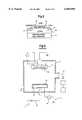
- FIG. 6shows a schematic view of a PECVD apparatus as an example of conventional thin film deposition apparatuses.
- the apparatus shown in FIG. 6is mainly composed by process chamber 1 comprising a pumping system, substrate holder 2 for placing substrate 20 in process chamber 1, deposition gas introduction system 3 for introducing a deposition gas into process chamber 1 and electric power supplying means 4 to supply energy with the introduced deposition gas to generate a plasma.
- Deposition gas introduction system 3introduces the deposition gas through disc shaped gas introduction head 31 which is provided facing to substrate holder 2.
- Gas introduction head 31is hollow and has many gas effusion holes 32 at its front side.
- the end of pipe 33 introducing the deposition gasis connected with gas introduction head 31 so that the deposition gas can effuse from gas effusion holes 32 toward substrate 20.
- Electric power supplying means 4is composed so as to supply a radio frequency (RF) power as plasma generation energy.
- Gas introduction head 31is commonly used as an electrode for applying the RF.
- introduction head 31is made of conductor and is connected with RF source 41 interposing a matching box (not shown).
- the apparatus shown in FIG. 6is operated as follows.
- the deposition gasis introduced into process chamber 1 by deposition gas introduction system 3.
- Controlling a flow rate of the deposition gasan RF field is applied by RF source 41 from gas introduction head 31.
- This RF fieldignites a discharge with the deposition gas, thus transformed into plasma, which is utilized for thin film deposition on the surface of substrate 20.
- silicon nitride filmis deposited utilizing decomposition of silane (SiH 4 ) in the plasma which is generated by silane and ammonia (NH 3 ) gas mixture used as the deposition gas.
- materials of thin filmsare often dissimilar to underlayers.
- IGFETinsulated-gate field effect transistors
- an insulator filmis deposited on an underlying semiconductor and a gate is formed on the insulator film.
- an insulator filmis often deposited on a semiconductor surface for passivation.
- PECVD apparatuseshave little problem of interfacial defects caused by heat, because depositions are carried out under temperatures lower than normal thermal CVD apparatuses.
- PECVD apparatuseshave a problem that interfacial defects caused by incidence of high-energy charged particles produced in plasma. More specifically, when an insulator film is deposited on a substrate surface which suffered a physical damage such as local deformation caused by high-energy ions impingement onto the substrate surface, or when incidence of high-energy ions onto a deposited insulator film occurs, local deformation defects such as a pin hole are produced in the insulator film, which leads to the defect on product that breakdown may occur with its insulator film.
- ions or electronsare incorporated into an insulator film, resistance of the insulator film may decrease causing breakdown voltage fall.
- the incorporation of ions or electrons into an insulator filmleads to carrier implantation that causes electron traps, resulting in deterioration of device performance properties.
- PECVD apparatusescan deposit films at low temperatures compared with thermal CVD apparatuses, there is a limitation in lowering deposition temperature (temperature of a substrate during deposition), because the substrate is exposed to a plasma. Therefore, PECVD apparatuses probably can not satisfy the demand of further lowering of deposition temperature.
- deposition temperaturetemperature of a substrate during deposition
- GaAsgallium arsenide
- Prior PECVD apparatusessometimes have difficulty in operation at temperatures below 400° C.
- interfacial energy level densityis also a crucial technical matter with respect to state of insulator-semiconductor interface.
- the interfacial energy levelswhich are also called “interface traps” or “interface state” are inevitably generated on dissimilar materials junction such as semiconductor-insulator junction, namely heterojunction.
- interface trapsor “interface state”
- dissimilar materials junctionsuch as semiconductor-insulator junction, namely heterojunction.
- a problem that charging and discharging on the interfacial levelsthat is, traps and releases of electrons make a cause of noise and affect operation characteristics becomes serious.
- a surface depletion layeris formed resulting from high-density interfacial levels. The surface depletion layer influences generation of great parasitic resistance on the channel surface. This is a hurdle for higher function of devices.
- a native oxide layeris often formed on a semiconductor surface.
- a insulator filmis deposited on this native oxide layer, many levels are generated by this native oxide layer, which leads easily to high-density interfacial levels.
- depositionshould be carried out after removal of the native oxide layer.
- Sulfuric acid (H 2 SO 4 ) or hydrogen peroxide (H 2 O 2 )is used for the removal of the native oxide layer.
- H 2 SO 4sulfuric acid
- H 2 O 2hydrogen peroxide
- the object of the present inventionis to solve these problems described above. Specifically, the object of the present invention is to provide a method and apparatus where interfacial level density can be reduced effectively and deposition temperature can be lowered furthermore. Another object of the present invention is to provide a semiconductor device having a semiconductor-insulator junction of low interfacial level density.
- the present inventionprovides a method and apparatus where a pre-treatment which reduce interfacial level density is carried out before deposition utilizing a catalytic gas phase reaction. And, the present invention provides a semiconductor device having a semiconductor-insulator junction with its interfacial level density is 10 12 eV -1 cm -2 or less, which is brought by the pre-treatment in the insulator film deposition process.
- FIG. 1shows a schematic view of a thin film deposition apparatus of a mode of the invention.
- FIG. 2shows a schematic plane view of a thermal catalysis body employed with the apparatus of FIG. 1
- FIG. 3explains a model of film growth in catalytic CVD (CAT-CVD) methods.
- FIG. 4shows a result of an experiment confirming the effect of the pre-treatment.
- FIG. 5schematically shows a structure of a semiconductor device of a mode of the invention.
- FIG. 6shows a schematic view of a PECVD apparatus as an example of prior thin film deposition apparatuses.
- FIG. 1shows a schematic view of a thin film deposition apparatus of a mode of the invention.
- the apparatus shown in FIG. 1comprises a process chamber 1 in which a substrate 20 is placed, substrate holder 2 for placing substrate 20 in process chamber 1, deposition gas introduction system 3 for introducing a deposition gas into process chamber 1, a thermal catalysis body 5 provided near the substrate placement, at a location separated from the substrate a heater 51 for heating thermal catalysis body 5 up to a certain temperature.
- Process chamber 1is an air-tight vacuum chamber comprising a pumping system 11.
- Pumping system 11is a multi-stage type system which uses multiple vacuum pumps such as a combination of a turbo-molecular pump and a mechanical-sealed pump. Pumping system 11 can pump process chamber 1 to order of 10 -8 Torr.
- Substrate holder 2is provided at the upper wall of process chamber 1. Substrate 20 is held on the lower surface of substrate holder 2. Holding of substrate 20 is carried out by an electrostatic chucking method inducing static charges on the lower surface of substrate holder 2, or a mechanical chucking method using a clamp which cross-section shape is "L".
- Heater 21 for heating substrate 20 up to a certain temperatureis provided in substrate holder 2.
- a resistance heating type heateris typically used as heater 21.
- Heater 21is connected with power supply 22 provided outside process chamber 1.
- Power supply 22is equipped with control unit (not shown) which controls the input power to heater 21 according to a output signal from a temperature monitor (not shown) monitoring temperature of substrate 20 or substrate holder 2.
- Thermal catalysis body 5characterizes the apparatus of this mode. Thermal catalysis body 5 is employed so that deposition is carried out utilizing a gas-phase reaction of the deposition gas without using plasma.
- FIG. 2shows a schematic plane view of thermal catalysis body 5 employed in the apparatus of FIG. 1. In this mode, 0.5 mm diameter tungsten wire is used as thermal catalysis body 5.
- the tungsten wire as thermal catalysis body 5is formed into a saw-tooth-wave shape shown in FIG. 2 and fixed with square-shaped frame 52 which is a little larger than substrate 20. Frame 52 is made of molybdenum.
- the distance between thermal catalysis body 5 and substrate 20is, for example, 20 cm. Thermal catalysis body 5 is desirably provided close to substrate 20 because the effect of a catalytic reaction (described after) is decreased if the distance between thermal catalytic body 5 and substrate 20 is wider.
- Heater 51which heats thermal catalysis body 5 is composed mainly by a resistance heating power supply letting a current flow through the tungsten wire. Thermal catalysis body 5 is heated up to, for example, 1700° C. by heater 51.
- Deposition gas introduction system 3comprises pipe 33 introducing the deposition gas to process chamber 1, and valve 34 and gas flow controller (not shown) provided on pipe 33.
- disc-shaped gas introduction head 31is provided facing to substrate holder 2 in process chamber 1.
- Gas introduction head 31is hollow and has many gas effusion holes 32 at its front side. The end of pipe 33 is connected with gas introduction head 31 so that the deposition gas can effuse from gas effusion holes 32 for substrate 20.
- the deposition gas effusing from gas effusion holes 32are supplied with substrate 20 via thermal catalysis body 5. This results in that a thin film is deposited on the surface of substrate 20 utilizing a catalytic gas-phase reaction of the deposition gas by thermal catalysis body 5.
- FIG. 3explains the model of the film growth in CAT-CVD.
- gas mixturesuch as silane and ammonium gas mixture is used as the deposition gas.
- silane gaspasses by thermal catalysis body 5
- a contact decomposition reactionsimilar to the adsorptive dissociation reaction of hydrogen molecular takes place. This contact decomposition reaction produces fractional radicals SiH 3 * and H*.
- suffix (g)means "gas phase” and suffix (s) means "solid phase”.
- Film deposition by the CAT-CVD methoddoes not use plasmas. Therefore, the CAT-CVD is essentially free from problems such as the substrate surface damage by incidence of high-energy charged particles from plasma and deterioration of insulator film by incorporation of charged particles as demonstrated in PECVD apparatuses.
- the CAT-CVDhas another advantage that lower-temperature processes are possible because the substrate is not exposed to plasma.
- thermal catalysis body 5is commonly used for a pre-treatment that reduces interfacial defects. This point is described in detail as follows.
- hydrogen gaswhen hydrogen gas is introduced from gas introduction head 31, hydrogen gas is activated by the contact decomposition reaction on thermal catalysis body 5, producing hydrogen radicals.
- hydrogen radicalsBy these hydrogen radicals a surface cleaning that removes a native oxide layer on a substrate surface is possible.
- a substrate surfaceis gallium arsenide semiconductor
- hydrogen radicalsreact with oxygen (O) in the native oxide layer formed on the gallium arsenide surface to dissociate O from gallium arsenide.
- Oxygenreacts hydrogen radicals to form H 2 O which is evacuated from process chamber 1 by pumping system 11. This is expressed as;
- Ga--NAs--N
- As--NAs--N
- recombination of gallium arsenide and released oxygendoes not occur.
- Ga--N (or As--N) bondis easily dissociated when thin film is deposited on it. This also contributes to flattening of the GaAs-film interface.
- the apparatus of this modecomprises treatment gas introduction system 6.
- Treatment gas introduction system 6is connected with deposition gas introduction system 3.
- part of deposition gas introduction system 3may be commonly used for a treatment gas introduction system.
- deposition gasis silane-ammonium gas mixture and treatment gas is hydrogen
- pipe 61 of treatment gas introduction system 6is connected with pipe 33 of deposition gas introduction system 3.
- the treatment gasis introduced switching from the deposition gas by operation of valve 34 and 62.
- treatment gasis partly common to deposition gas
- the deposition gasis silane-ammonium gas mixture and the treatment gas is ammonium
- introduction of the treatment gasis carried out commonly using a part of deposition gas introduction system 3.
- only the treatment gascan be introduced by operation of valve 34 in deposition gas introduction system 3.
- Ammoniumis one example of nitrogen bearing gases.
- nitrogen gas and nitrogen compound gassuch as hydrazine (N 2 H 4 ) are included in "nitrogen bearing gases" other than ammonium.
- a treatment gaseffuses from gas effusion holes 32 of gas introduction head 31 and is supplied with substrate 20.
- a treatment gasflows near or on the surface of thermal catalysis body 5, resulting in that a treatment is carried out on the substrate surface by a contact decomposition reaction as described.
- FIG. 4shows a result of an experiment confirming the effect of the pre-treatment.
- the treatment confirmed in this experimentis the surface cleaning that a native oxide layer on a gallium arsenide semiconductor surface is removed by the hydrogen radicals as described.
- (a)is a result of observation of the gallium arsenide semiconductor surface before the treatment by the X-ray photoelectron spectroscopy (XPS) method.
- (a)demonstrates the existence of Ga--O bond and As--O bond (designated by ⁇ plotting) in gallium arsenide.
- (b) in FIG. 4is a result of observation of the gallium arsenide semiconductor surface after the treatment by the XPS method.
- substrate 20is transferred into process chamber 1 through a gate-valve (not shown) and is held by substrate holder 2.
- Process chamber 1is pumped by pumping system 11 to a certain pressure.
- Heater 21heats is substrate 20 up to a certain temperature.
- treatment gas introduction system 6is operated so as to introduce a treatment gas into process chamber 1.
- the introduced treatment gasarrives at substrate 20 via thermal catalysis body. This results in that a contact decomposition reaction takes place and a treatment is carried out on the surface of substrate 20 utilizing this reaction.
- deposition gas introduction system 3is operated so as to introduce a deposition gas into process chamber 1.
- the introduced deposition gasis supplied with substrate 20 via thermal catalyst body 5. This results in that another contact decomposition reaction takes place and a thin film deposition is carried out on the surface of substrate 20 utilizing this reaction.
- the CAT-CVD filmgrows on the pre-treated clean surface which is not contaminated, because the pre-treatment and the deposition are carried out continuously in the same process chamber 1. Therefore, this process is very effective for reduction of interfacial defects. If another process is interposed or substrate 20 is exposed to atmosphere between the pre-treatment and the deposition, the surface of substrate 20 may suffer contamination such as native re-oxidation, which diminishes the technically advantageous effect of the pre-treatment.
- Deposition temperatureis a significant parameter in the process described above. For example, if deposition temperature exceeds 400° C. in film depositions on a semiconductor of gallium arsenide series, the semiconductor surface becomes rough because arsenic atoms thermally dissociate from gallium arsenide. Many kinds of interfacial defects are produced when an insulator film is deposited on such a rough surface as this. Therefore, the deposition temperature in this case is significantly kept below 400° C.
- temperature of substrate 20is preferably kept lower than a critical value where substrate 20 suffers thermal degradation in general.
- temperature of substrate 20 during depositionis preferably kept below the melting point of the wiring material.
- FIG. 5schematically shows a structure of a semiconductor device of a mode of the invention.
- the semiconductor device of the inventionis one having a semiconductor-insulator junction where a insulator film is deposited on an underlying semiconductor.
- semiconductorshaving such a structure as this.
- FIG. 5shows a structure of a IGFET as an example.
- the semiconductor device shown in FIG. 5have a structure where n + source-drain 73,74 are formed with p 31 -GaAs region 72 on semi-insulating GaAs substrate 71, and gate 76 is formed between source 73 and drain 74 interposing insulation film 75.
- This semiconductor deviceis operated on the inversion-accumulation mode as well as normal MOS-FETs.
- bias voltageis applied from gate 76 through insulation film 75, an inversion region is formed on the p - -GaAs region 72 to become a n-channel which makes operation of the FET possible.
- IGFETinterfacial energy level
- prior semiconductor devices of gallium arsenide seriesinterfacial energy level densities are 10 13 eV -1 cm -2 or more. So, the semiconductor device of this mode has achieved the interfacial level density reduction more than one order. This means that the operation of IGFET, which has been thought impossible, becomes possible.
- IGFET of gallium arsenide serieshas the advantage that circuit design can have large variety because there is no leak current from the gate, compared to metal-semiconductor FET (MESFET) which is widely used in ICs.
- MESFETmetal-semiconductor FET
- insulator film 75is silicon nitride film and gate 76 is made of aluminum.
- the interfacial level densitycan be measured from capacitance-voltage characteristic of such a metal-insulator-semiconductor multilayer structure (MIS structure) as this.
- MIS structuremetal-insulator-semiconductor multilayer structure
- any semiconductor devices having a semiconductor-insulator junction other than the described IGFETcan be adopted.
- Passivation by depositing a insulator film on a semiconductor surfaceis widely carried out. Depositing this passivation film by the method and apparatus of the invention, low-density interfacial level junction is obtained, which contributes to diminishing problems caused by interfacial traps such as generation of noise.
- Si, Ge, SiGe, SiC, GaAlAs, GaP, InP, ZnSe or CdSalso can be used as material of the underlying semiconductor other than gallium arsenide (GaAs).
- Silicon oxide film, silicon oxygen nitride film, aluminum nitride film or aluminum oxide filmalso can be used as the insulator film other than silicon nitride film.
- the idea of the inventionis in depositing a thin film on a substrate surface of material dissimilar to the thin film, namely heterojunction. So, the invention can be modified into a composition where a metal film is deposited on a semiconductor surface or an insulator film is deposited on a metal surface. There is another modification where a semiconductor film is deposited on an underlying semiconductor of dissimilar material.
- reduction of interfacial defects or the interfacial level densityis the general demand. Therefore, the invention satisfying this demand has great significance.
- the thin film deposition after the pre-treatmentmay be carried out by a method other than CAT-CVD.
- PECVD or other thermal CVDmay be employed in case that damage by plasma makes no problem or higher deposition temperature is allowed.
- the thermal catalysis body in the inventionmay be made of molybdenum, tantalum, titanium or vanadium other than tungsten. In studies by the inventors, the thermally catalytic effects with these materials were confirmed. Any shapes of the thermal catalysis body such as a spiral, swirl or mesh may be employed other than the saw-tooth-wave. A blade- or rod-shaped thermal catalysis body also may be used other than using a wire. A treatment such as electrolytic polishing is given on the surface of the thermal catalysis body if necessary. When the thermal catalysis body is used at temperatures over 1500° C. introducing a silicon compound gas such as silane, silicide is occasionally formed on the surface of the thermal catalysis body. In this case, the thermal catalysis body is preferably replaced with a new one or one having a clean surface.
Landscapes
- Engineering & Computer Science (AREA)
- Physics & Mathematics (AREA)
- Condensed Matter Physics & Semiconductors (AREA)
- General Physics & Mathematics (AREA)
- Manufacturing & Machinery (AREA)
- Computer Hardware Design (AREA)
- Microelectronics & Electronic Packaging (AREA)
- Power Engineering (AREA)
- Chemical & Material Sciences (AREA)
- Chemical Kinetics & Catalysis (AREA)
- General Chemical & Material Sciences (AREA)
- Materials Engineering (AREA)
- Mechanical Engineering (AREA)
- Metallurgy (AREA)
- Organic Chemistry (AREA)
- Formation Of Insulating Films (AREA)
Abstract
Description
SiH.sub.4(g) →SiH.sub.3 *.sub.(g) +H*.sub.(g)
NH.sub.3(g) →NH.sub.2 *.sub.(g) +H*.sub.(g)
aSiH.sub.3 *.sub.(g) +bNH.sub.2 *.sub.(g) →cSiN.sub.x(s)
H.sub.2 →2H*
2H*+Ga--O (or As--O)→Ga (or As)+H.sub.2 O.sub.(g)
NH.sub.3 →NH.sub.2 *+H*
NH.sub.2 *+Ga--O (or As--O)→Ga--N (or As--N)+H.sub.2 O.sub.(g)
Claims (13)
Priority Applications (2)
| Application Number | Priority Date | Filing Date | Title |
|---|---|---|---|
| US09/102,665US6349669B1 (en) | 1996-09-06 | 1998-06-23 | Method and apparatus for depositing a thin film, and semiconductor device having a semiconductor-insulator junction |
| US10/041,609US6723664B2 (en) | 1996-06-09 | 2002-01-10 | Method and apparatus for depositing a thin film, and semiconductor device having a semiconductor-insulator junction |
Applications Claiming Priority (2)
| Application Number | Priority Date | Filing Date | Title |
|---|---|---|---|
| JP8-257675 | 1996-09-06 | ||
| JP25767596AJP3737221B2 (en) | 1996-09-06 | 1996-09-06 | Thin film forming method and thin film forming apparatus |
Related Child Applications (1)
| Application Number | Title | Priority Date | Filing Date |
|---|---|---|---|
| US09/102,665DivisionUS6349669B1 (en) | 1996-06-09 | 1998-06-23 | Method and apparatus for depositing a thin film, and semiconductor device having a semiconductor-insulator junction |
Publications (1)
| Publication Number | Publication Date |
|---|---|
| US6069094Atrue US6069094A (en) | 2000-05-30 |
Family
ID=17309550
Family Applications (3)
| Application Number | Title | Priority Date | Filing Date |
|---|---|---|---|
| US08/924,304Expired - LifetimeUS6069094A (en) | 1996-06-09 | 1997-09-05 | Method for depositing a thin film |
| US09/102,665Expired - LifetimeUS6349669B1 (en) | 1996-06-09 | 1998-06-23 | Method and apparatus for depositing a thin film, and semiconductor device having a semiconductor-insulator junction |
| US10/041,609Expired - LifetimeUS6723664B2 (en) | 1996-06-09 | 2002-01-10 | Method and apparatus for depositing a thin film, and semiconductor device having a semiconductor-insulator junction |
Family Applications After (2)
| Application Number | Title | Priority Date | Filing Date |
|---|---|---|---|
| US09/102,665Expired - LifetimeUS6349669B1 (en) | 1996-06-09 | 1998-06-23 | Method and apparatus for depositing a thin film, and semiconductor device having a semiconductor-insulator junction |
| US10/041,609Expired - LifetimeUS6723664B2 (en) | 1996-06-09 | 2002-01-10 | Method and apparatus for depositing a thin film, and semiconductor device having a semiconductor-insulator junction |
Country Status (4)
| Country | Link |
|---|---|
| US (3) | US6069094A (en) |
| JP (1) | JP3737221B2 (en) |
| KR (1) | KR19980024396A (en) |
| TW (1) | TW344099B (en) |
Cited By (22)
| Publication number | Priority date | Publication date | Assignee | Title |
|---|---|---|---|---|
| US6218301B1 (en)* | 2000-07-31 | 2001-04-17 | Applied Materials, Inc. | Deposition of tungsten films from W(CO)6 |
| US6349669B1 (en)* | 1996-09-06 | 2002-02-26 | Hideki Matsumura | Method and apparatus for depositing a thin film, and semiconductor device having a semiconductor-insulator junction |
| WO2002025712A1 (en)* | 2000-09-14 | 2002-03-28 | Japan As Represented By President Of Japan Advanced Institute Of Science And Technology | Heating element cvd device |
| US6376340B1 (en) | 1999-03-16 | 2002-04-23 | Sony Corporation | Methods for forming polycrystalline silicon film |
| US6468885B1 (en)* | 1996-09-26 | 2002-10-22 | Midwest Research Institute | Deposition of device quality, low hydrogen content, hydrogenated amorphous silicon at high deposition rates |
| US20030124874A1 (en)* | 2001-05-09 | 2003-07-03 | Nobuo Matsuki | Method of forming low dielectric constant insulation film for semiconductor device |
| US20030194881A1 (en)* | 2002-04-15 | 2003-10-16 | Mitsubishi Denki Kabushiki Kaisha | Process for manufacturing a semiconductor device |
| US6653212B1 (en)* | 1999-04-20 | 2003-11-25 | Sony Corporation | Method and apparatus for thin-film deposition, and method of manufacturing thin-film semiconductor device |
| US20040015946A1 (en)* | 2000-06-01 | 2004-01-22 | Moddy Te'eni | Method for resolving dependency conflicts among multiple operative entities within a computing environment |
| US20040065260A1 (en)* | 2002-10-04 | 2004-04-08 | Anelva Corporation | Heating element CVD system and connection structure between heating element and electric power supply mechanism in the heating element CVD system |
| WO2004100273A1 (en) | 2003-05-09 | 2004-11-18 | Shin-Etsu Handotai Co., Ltd. | Solar cell and process for producing the same |
| US20050196977A1 (en)* | 2004-03-02 | 2005-09-08 | Semiconductor Leading Edge Technologies, Inc. | Method of forming silicon nitride film and method of manufacturing semiconductor device |
| US20070128861A1 (en)* | 2005-12-05 | 2007-06-07 | Kim Myoung S | CVD apparatus for depositing polysilicon |
| US20070187812A1 (en)* | 2004-06-07 | 2007-08-16 | Akira Izumi | Method for processing copper surface, method for forming copper pattern wiring and semiconductor device manufactured using such method |
| US20080261348A1 (en)* | 2007-04-23 | 2008-10-23 | Sanyo Electric Co., Ltd. | Method of manufacturing semiconductor film and method of manufacturing photovoltaic element |
| US20100087050A1 (en)* | 2008-10-03 | 2010-04-08 | Veeco Instruments Inc. | Chemical vapor deposition with energy input |
| US20100105214A1 (en)* | 2007-05-30 | 2010-04-29 | Mitsubishi Electric Corporation | Method of manufacturing semiconductor device |
| US20110012178A1 (en)* | 2008-03-26 | 2011-01-20 | Masakazu Sugiyama | Semiconductor wafer, method of manufacturing a semiconductor wafer, and semiconductor device |
| US20110100955A1 (en)* | 2009-09-18 | 2011-05-05 | Applied Materials, Inc. | Apparatus and methods for forming energy storage and photovoltaic devices in a linear system |
| US9306026B2 (en) | 2012-08-24 | 2016-04-05 | Japan Science And Technology Agency | Semiconductor structure having aluminum oxynitride film on germanium layer and method of fabricating the same |
| JP2016136601A (en)* | 2015-01-23 | 2016-07-28 | 東京エレクトロン株式会社 | Substrate processing equipment |
| US12422754B2 (en) | 2020-09-04 | 2025-09-23 | Samsung Electronics Co., Ltd. | Substrate processing apparatus, semiconductor manufacturing equipment, and substrate processing method |
Families Citing this family (38)
| Publication number | Priority date | Publication date | Assignee | Title |
|---|---|---|---|---|
| KR100321715B1 (en)* | 1998-10-13 | 2002-03-08 | 박종섭 | A method for fabricating semiconductor device using AlN film as diffusion barrier and method for forming bottom electrode of capacitor using thereof |
| JP4573921B2 (en)* | 1999-01-21 | 2010-11-04 | 富士通セミコンダクター株式会社 | Manufacturing method of semiconductor device |
| TW455912B (en) | 1999-01-22 | 2001-09-21 | Sony Corp | Method and apparatus for film deposition |
| JP4505072B2 (en)* | 1999-03-25 | 2010-07-14 | 独立行政法人科学技術振興機構 | Chemical vapor deposition method and chemical vapor deposition apparatus |
| JP4505073B2 (en)* | 1999-03-25 | 2010-07-14 | 独立行政法人科学技術振興機構 | Chemical vapor deposition equipment |
| JP4459329B2 (en) | 1999-08-05 | 2010-04-28 | キヤノンアネルバ株式会社 | Method and apparatus for removing attached film |
| JP4346741B2 (en) | 1999-08-05 | 2009-10-21 | キヤノンアネルバ株式会社 | Heating element CVD apparatus and method for removing attached film |
| JP3341763B2 (en)* | 2000-04-27 | 2002-11-05 | 住友電気工業株式会社 | Method for manufacturing compound semiconductor device and apparatus for manufacturing compound semiconductor device |
| JP2002069646A (en)* | 2000-09-01 | 2002-03-08 | Sony Corp | Thin film manufacturing method |
| JP4599734B2 (en)* | 2001-03-14 | 2010-12-15 | ソニー株式会社 | Method for forming polycrystalline semiconductor thin film and method for manufacturing semiconductor device |
| JP2002299238A (en)* | 2001-04-04 | 2002-10-11 | Sony Corp | Method for forming polycrystalline semiconductor thin film and method for manufacturing semiconductor device |
| JP4599746B2 (en)* | 2001-04-04 | 2010-12-15 | ソニー株式会社 | Method for forming polycrystalline semiconductor thin film and method for manufacturing semiconductor device |
| JP4644964B2 (en)* | 2001-04-04 | 2011-03-09 | ソニー株式会社 | Method for forming polycrystalline semiconductor thin film and method for manufacturing semiconductor device |
| JP2002353184A (en)* | 2001-05-28 | 2002-12-06 | Tokyo Electron Ltd | Substrate processing method and substrate processor |
| US7122736B2 (en)* | 2001-08-16 | 2006-10-17 | Midwest Research Institute | Method and apparatus for fabricating a thin-film solar cell utilizing a hot wire chemical vapor deposition technique |
| US6489238B1 (en)* | 2001-08-21 | 2002-12-03 | Texas Instruments Incorporated | Method to reduce photoresist contamination from silicon carbide films |
| US6861326B2 (en)* | 2001-11-21 | 2005-03-01 | Micron Technology, Inc. | Methods of forming semiconductor circuitry |
| JP4011376B2 (en)* | 2002-03-20 | 2007-11-21 | 日本エー・エス・エム株式会社 | Method for forming interlayer insulating film |
| JP4157718B2 (en) | 2002-04-22 | 2008-10-01 | キヤノンアネルバ株式会社 | Silicon nitride film manufacturing method and silicon nitride film manufacturing apparatus |
| EP1637221A4 (en) | 2003-03-19 | 2008-01-23 | Tosoh Corp | BODY WITH MICRO CHANNEL STRUCTURE |
| JP4620333B2 (en)* | 2003-05-09 | 2011-01-26 | 三菱電機株式会社 | Manufacturing method of semiconductor device |
| TW200603287A (en)* | 2004-03-26 | 2006-01-16 | Ulvac Inc | Unit layer posttreating catalytic chemical vapor deposition apparatus and method of film formation therewith |
| JP2006093242A (en)* | 2004-09-21 | 2006-04-06 | Sanyo Electric Co Ltd | Method of manufacturing semiconductor device |
| KR100700493B1 (en)* | 2005-05-24 | 2007-03-28 | 삼성에스디아이 주식회사 | Catalytically Enhanced Chemical Vapor Deposition Equipment with Efficient Filament Array Structure |
| US9157152B2 (en)* | 2007-03-29 | 2015-10-13 | Tokyo Electron Limited | Vapor deposition system |
| US20090226614A1 (en)* | 2008-03-04 | 2009-09-10 | Tokyo Electron Limited | Porous gas heating device for a vapor deposition system |
| JP4705668B2 (en)* | 2008-08-25 | 2011-06-22 | 独立行政法人科学技術振興機構 | Chemical vapor deposition method using chemical vapor deposition equipment |
| JP4866402B2 (en)* | 2008-08-25 | 2012-02-01 | 独立行政法人科学技術振興機構 | Chemical vapor deposition method |
| US8524562B2 (en)* | 2008-09-16 | 2013-09-03 | Imec | Method for reducing Fermi-Level-Pinning in a non-silicon channel MOS device |
| JP2009111397A (en)* | 2008-11-04 | 2009-05-21 | Canon Anelva Corp | Etching method of adhesion film |
| JP2009044190A (en)* | 2008-11-07 | 2009-02-26 | Canon Anelva Corp | Etching method of adhesion film |
| JP4866446B2 (en)* | 2009-07-09 | 2012-02-01 | 独立行政法人科学技術振興機構 | Catalytic chemical vapor deposition apparatus and thin film manufacturing method |
| US20120312326A1 (en)* | 2011-06-10 | 2012-12-13 | Applied Materials, Inc. | Methods for cleaning a surface of a substrate using a hot wire chemical vapor deposition (hwcvd) chamber |
| JP2013165144A (en)* | 2012-02-10 | 2013-08-22 | Nippon Telegr & Teleph Corp <Ntt> | Method for manufacturing mos structure |
| JP2014029908A (en)* | 2012-07-31 | 2014-02-13 | Toyota Central R&D Labs Inc | Semiconductor device and semiconductor device manufacturing method |
| KR20140032253A (en)* | 2012-09-06 | 2014-03-14 | 한국전자통신연구원 | Touch screen and manufacturing method of the same |
| KR101386135B1 (en)* | 2012-11-29 | 2014-04-17 | 한국전기연구원 | Manufacturing method for decreasing interface states of sic/sio2 interface |
| WO2025117601A1 (en)* | 2023-11-27 | 2025-06-05 | Lam Research Corporation | Forming aluminum nitride coating on aluminum-containing metal |
Citations (8)
| Publication number | Priority date | Publication date | Assignee | Title |
|---|---|---|---|---|
| US3652331A (en)* | 1968-03-22 | 1972-03-28 | Shumpei Yamazaki | Process for forming a film on the surface of a substrate by a gas phase |
| US4237150A (en)* | 1979-04-18 | 1980-12-02 | The United States Of America As Represented By The United States Department Of Energy | Method of producing hydrogenated amorphous silicon film |
| JPS6340314A (en)* | 1986-08-05 | 1988-02-20 | Hiroshima Univ | Manufacture of thin film by catalytic cvd method and device therefor |
| US5160544A (en)* | 1990-03-20 | 1992-11-03 | Diamonex Incorporated | Hot filament chemical vapor deposition reactor |
| US5366919A (en)* | 1992-10-14 | 1994-11-22 | Nippon Steel Corporation | Method of making a memory cell of a semiconductor memory device |
| US5397737A (en)* | 1992-05-05 | 1995-03-14 | The United States Of America As Represented By The United States Department Of Energy | Deposition of device quality low H content, amorphous silicon films |
| US5795828A (en)* | 1994-07-14 | 1998-08-18 | Matsushita Electric Industrial Co., Ltd. | Electroless plating bath used for forming a wiring of a semiconductor device, and method of forming a wiring of a semiconductor device |
| US5840600A (en)* | 1994-08-31 | 1998-11-24 | Semiconductor Energy Laboratory Co., Ltd. | Method for producing semiconductor device and apparatus for treating semiconductor device |
Family Cites Families (9)
| Publication number | Priority date | Publication date | Assignee | Title |
|---|---|---|---|---|
| US4231750A (en)* | 1977-12-13 | 1980-11-04 | Diagnostic Reagents, Inc. | Methods for performing chemical assays using fluorescence and photon counting |
| KR900005118B1 (en)* | 1986-07-14 | 1990-07-19 | 미쓰비시전기주식회사 | Device for forming thin compound film |
| DE3923390A1 (en)* | 1988-07-14 | 1990-01-25 | Canon Kk | DEVICE FOR FORMING A LARGE Vaporized VAPOR FILM USING AT LEAST TWO SEPARATELY DETERMINED ACTIVATED GASES |
| US5209812A (en)* | 1990-04-09 | 1993-05-11 | Ford Motor Company | Hot filament method for growing high purity diamond |
| US5186973A (en)* | 1990-09-13 | 1993-02-16 | Diamonex, Incorporated | HFCVD method for producing thick, adherent and coherent polycrystalline diamonds films |
| US5183529A (en)* | 1990-10-29 | 1993-02-02 | Ford Motor Company | Fabrication of polycrystalline free-standing diamond films |
| FR2727433B1 (en)* | 1994-11-30 | 1997-01-03 | Kodak Pathe | PROCESS FOR THE MANUFACTURE OF BORON-DOPED DIAMOND LAYERS |
| US5693173A (en)* | 1994-12-21 | 1997-12-02 | Chorus Corporation | Thermal gas cracking source technology |
| JP3737221B2 (en)* | 1996-09-06 | 2006-01-18 | 英樹 松村 | Thin film forming method and thin film forming apparatus |
- 1996
- 1996-09-06JPJP25767596Apatent/JP3737221B2/ennot_activeExpired - Lifetime
- 1997
- 1997-09-05USUS08/924,304patent/US6069094A/ennot_activeExpired - Lifetime
- 1997-09-05KRKR1019970046036Apatent/KR19980024396A/ennot_activeCeased
- 1997-09-05TWTW086112830Apatent/TW344099B/ennot_activeIP Right Cessation
- 1998
- 1998-06-23USUS09/102,665patent/US6349669B1/ennot_activeExpired - Lifetime
- 2002
- 2002-01-10USUS10/041,609patent/US6723664B2/ennot_activeExpired - Lifetime
Patent Citations (8)
| Publication number | Priority date | Publication date | Assignee | Title |
|---|---|---|---|---|
| US3652331A (en)* | 1968-03-22 | 1972-03-28 | Shumpei Yamazaki | Process for forming a film on the surface of a substrate by a gas phase |
| US4237150A (en)* | 1979-04-18 | 1980-12-02 | The United States Of America As Represented By The United States Department Of Energy | Method of producing hydrogenated amorphous silicon film |
| JPS6340314A (en)* | 1986-08-05 | 1988-02-20 | Hiroshima Univ | Manufacture of thin film by catalytic cvd method and device therefor |
| US5160544A (en)* | 1990-03-20 | 1992-11-03 | Diamonex Incorporated | Hot filament chemical vapor deposition reactor |
| US5397737A (en)* | 1992-05-05 | 1995-03-14 | The United States Of America As Represented By The United States Department Of Energy | Deposition of device quality low H content, amorphous silicon films |
| US5366919A (en)* | 1992-10-14 | 1994-11-22 | Nippon Steel Corporation | Method of making a memory cell of a semiconductor memory device |
| US5795828A (en)* | 1994-07-14 | 1998-08-18 | Matsushita Electric Industrial Co., Ltd. | Electroless plating bath used for forming a wiring of a semiconductor device, and method of forming a wiring of a semiconductor device |
| US5840600A (en)* | 1994-08-31 | 1998-11-24 | Semiconductor Energy Laboratory Co., Ltd. | Method for producing semiconductor device and apparatus for treating semiconductor device |
Non-Patent Citations (2)
| Title |
|---|
| S. Yamazaki et al. "Silicon Nitride Prepared by the SiH4 -NH3 Reaction with Catalysts", Japanese Journal of Applied Physics, vol. 9, No. 12, Dec. 1970, pp. 1467-1477. |
| S. Yamazaki et al. Silicon Nitride Prepared by the SiH 4 NH 3 Reaction with Catalysts , Japanese Journal of Applied Physics, vol. 9, No. 12, Dec. 1970, pp. 1467 1477.* |
Cited By (41)
| Publication number | Priority date | Publication date | Assignee | Title |
|---|---|---|---|---|
| US6723664B2 (en) | 1996-06-09 | 2004-04-20 | Hideki Matsumura | Method and apparatus for depositing a thin film, and semiconductor device having a semiconductor-insulator junction |
| US6349669B1 (en)* | 1996-09-06 | 2002-02-26 | Hideki Matsumura | Method and apparatus for depositing a thin film, and semiconductor device having a semiconductor-insulator junction |
| US20020086557A1 (en)* | 1996-09-06 | 2002-07-04 | Hideki Matsumura | Method and apparatus for depositing a thin film, and semiconductor device having a semiconductor-insulator junction |
| US6468885B1 (en)* | 1996-09-26 | 2002-10-22 | Midwest Research Institute | Deposition of device quality, low hydrogen content, hydrogenated amorphous silicon at high deposition rates |
| US6376340B1 (en) | 1999-03-16 | 2002-04-23 | Sony Corporation | Methods for forming polycrystalline silicon film |
| US6653212B1 (en)* | 1999-04-20 | 2003-11-25 | Sony Corporation | Method and apparatus for thin-film deposition, and method of manufacturing thin-film semiconductor device |
| US20040015946A1 (en)* | 2000-06-01 | 2004-01-22 | Moddy Te'eni | Method for resolving dependency conflicts among multiple operative entities within a computing environment |
| US7140013B2 (en)* | 2000-06-01 | 2006-11-21 | Aduva, Inc. | Component upgrading with dependency conflict resolution, knowledge based and rules |
| US6218301B1 (en)* | 2000-07-31 | 2001-04-17 | Applied Materials, Inc. | Deposition of tungsten films from W(CO)6 |
| US6593548B2 (en) | 2000-09-14 | 2003-07-15 | Japan As Represented By President Of Japan Advanced Institute Of Science And Technology | Heating element CVD system |
| WO2002025712A1 (en)* | 2000-09-14 | 2002-03-28 | Japan As Represented By President Of Japan Advanced Institute Of Science And Technology | Heating element cvd device |
| US6602800B2 (en)* | 2001-05-09 | 2003-08-05 | Asm Japan K.K. | Apparatus for forming thin film on semiconductor substrate by plasma reaction |
| US20030124874A1 (en)* | 2001-05-09 | 2003-07-03 | Nobuo Matsuki | Method of forming low dielectric constant insulation film for semiconductor device |
| US6737366B2 (en)* | 2001-05-09 | 2004-05-18 | Asm Japan K.K. | Method of forming low dielectric constant insulation film for semiconductor device |
| US20030194881A1 (en)* | 2002-04-15 | 2003-10-16 | Mitsubishi Denki Kabushiki Kaisha | Process for manufacturing a semiconductor device |
| EP1357587A1 (en)* | 2002-04-15 | 2003-10-29 | Mitsubishi Denki Kabushiki Kaisha | Process for catalytic chemical vapor deposition |
| US6933250B2 (en)* | 2002-04-15 | 2005-08-23 | Mitsubishi Denki Kabushiki Kaisha | Process for manufacturing a semiconductor device |
| US20040065260A1 (en)* | 2002-10-04 | 2004-04-08 | Anelva Corporation | Heating element CVD system and connection structure between heating element and electric power supply mechanism in the heating element CVD system |
| US7211152B2 (en)* | 2002-10-04 | 2007-05-01 | Anelva Corporation | Heating element CVD system and connection structure between heating element and electric power supply mechanism in the heating element CVD system |
| EP1630873A4 (en)* | 2003-05-09 | 2007-03-14 | Shinetsu Handotai Kk | SOLAR CELL AND METHOD OF MANUFACTURING THE SAME |
| US8030223B2 (en) | 2003-05-09 | 2011-10-04 | Shin-Etsu Chemical Co., Ltd. | Solar cell and method of fabricating the same |
| WO2004100273A1 (en) | 2003-05-09 | 2004-11-18 | Shin-Etsu Handotai Co., Ltd. | Solar cell and process for producing the same |
| US20100173447A1 (en)* | 2003-05-09 | 2010-07-08 | Shin-Etsu Chemical Co., Ltd. | Solar cell and method of fabricating the same |
| US20070186970A1 (en)* | 2003-05-09 | 2007-08-16 | Masatoshi Takahashi | Solar cell and method of fabricating the same |
| US7510984B2 (en)* | 2004-03-02 | 2009-03-31 | Ulvac, Inc. | Method of forming silicon nitride film and method of manufacturing semiconductor device |
| US20050196977A1 (en)* | 2004-03-02 | 2005-09-08 | Semiconductor Leading Edge Technologies, Inc. | Method of forming silicon nitride film and method of manufacturing semiconductor device |
| US20070187812A1 (en)* | 2004-06-07 | 2007-08-16 | Akira Izumi | Method for processing copper surface, method for forming copper pattern wiring and semiconductor device manufactured using such method |
| US7825026B2 (en)* | 2004-06-07 | 2010-11-02 | Kyushu Institute Of Technology | Method for processing copper surface, method for forming copper pattern wiring and semiconductor device manufactured using such method |
| US20070128861A1 (en)* | 2005-12-05 | 2007-06-07 | Kim Myoung S | CVD apparatus for depositing polysilicon |
| US20080261348A1 (en)* | 2007-04-23 | 2008-10-23 | Sanyo Electric Co., Ltd. | Method of manufacturing semiconductor film and method of manufacturing photovoltaic element |
| US7807495B2 (en)* | 2007-04-23 | 2010-10-05 | Sanyo Electric Co., Ltd. | Method of manufacturing semiconductor film and method of manufacturing photovoltaic element |
| US20100105214A1 (en)* | 2007-05-30 | 2010-04-29 | Mitsubishi Electric Corporation | Method of manufacturing semiconductor device |
| US20110012178A1 (en)* | 2008-03-26 | 2011-01-20 | Masakazu Sugiyama | Semiconductor wafer, method of manufacturing a semiconductor wafer, and semiconductor device |
| US20100086703A1 (en)* | 2008-10-03 | 2010-04-08 | Veeco Compound Semiconductor, Inc. | Vapor Phase Epitaxy System |
| US20100087050A1 (en)* | 2008-10-03 | 2010-04-08 | Veeco Instruments Inc. | Chemical vapor deposition with energy input |
| US8815709B2 (en) | 2008-10-03 | 2014-08-26 | Veeco Instruments Inc. | Chemical vapor deposition with energy input |
| US20110100955A1 (en)* | 2009-09-18 | 2011-05-05 | Applied Materials, Inc. | Apparatus and methods for forming energy storage and photovoltaic devices in a linear system |
| US8334017B2 (en) | 2009-09-18 | 2012-12-18 | Applied Materials, Inc. | Apparatus and methods for forming energy storage and photovoltaic devices in a linear system |
| US9306026B2 (en) | 2012-08-24 | 2016-04-05 | Japan Science And Technology Agency | Semiconductor structure having aluminum oxynitride film on germanium layer and method of fabricating the same |
| JP2016136601A (en)* | 2015-01-23 | 2016-07-28 | 東京エレクトロン株式会社 | Substrate processing equipment |
| US12422754B2 (en) | 2020-09-04 | 2025-09-23 | Samsung Electronics Co., Ltd. | Substrate processing apparatus, semiconductor manufacturing equipment, and substrate processing method |
Also Published As
| Publication number | Publication date |
|---|---|
| US6723664B2 (en) | 2004-04-20 |
| JPH1083988A (en) | 1998-03-31 |
| JP3737221B2 (en) | 2006-01-18 |
| US6349669B1 (en) | 2002-02-26 |
| KR19980024396A (en) | 1998-07-06 |
| TW344099B (en) | 1998-11-01 |
| US20020086557A1 (en) | 2002-07-04 |
Similar Documents
| Publication | Publication Date | Title |
|---|---|---|
| US6069094A (en) | Method for depositing a thin film | |
| US4298629A (en) | Method for forming a nitride insulating film on a silicon semiconductor substrate surface by direct nitridation | |
| KR100924055B1 (en) | Production method for semiconductor device and substrate processing device | |
| KR101020116B1 (en) | Method and apparatus for forming high quality low temperature silicon nitride film | |
| US8951913B2 (en) | Method for removing native oxide and associated residue from a substrate | |
| US7820558B2 (en) | Semiconductor device and method of producing the semiconductor device | |
| KR100980528B1 (en) | Decarbonation treatment method, film formation method, and semiconductor device manufacturing method | |
| US20140011339A1 (en) | Method for removing native oxide and residue from a germanium or iii-v group containing surface | |
| US20070235421A1 (en) | Substrate treating method and production method for semiconductor device | |
| KR20040048483A (en) | Method of forming gate oxide layer in semiconductor devices | |
| KR101548129B1 (en) | Protection of conductors from oxidation in deposition chambers | |
| TW201843733A (en) | Etching method and etching device | |
| JP2006511087A (en) | Method and apparatus for forming a high quality low temperature silicon nitride layer | |
| US5861059A (en) | Method for selective growth of silicon epitaxial film | |
| JP2001189275A (en) | Semiconductor film forming method, and manufacturing method of thin-film semiconductor device | |
| JPH07263431A (en) | Formation of tantalum-containing high dielectric film | |
| Lucovsky et al. | Low-temperature plasma-assisted oxidation of Si: a new approach for creation of device-quality Si SiO2 interfaces with deposited dielectrics for applications in Si MOSFET technologies | |
| US20230178375A1 (en) | Methods for forming work function modulating layers | |
| JPH07235530A (en) | Method of forming insulating film | |
| JP2001168055A (en) | Semiconductor film forming method and thin film semiconductor device manufacturing method | |
| JP2001176806A (en) | Method for forming semiconductor film, and method for manufacturing semiconductor device | |
| JPH0869994A (en) | Method for manufacturing semiconductor device | |
| González Díaz | N-2 remote plasma cleaning of InP to improve SiNx: H/InP interface performance |
Legal Events
| Date | Code | Title | Description |
|---|---|---|---|
| AS | Assignment | Owner name:ANELVA CORPORATION, JAPAN Free format text:ASSIGNMENT OF ASSIGNORS INTEREST;ASSIGNORS:MATSUMURA, HIDEKI;IZUMI, AKIRA;MASUDA, ATSUSHI;AND OTHERS;REEL/FRAME:008790/0668 Effective date:19970827 Owner name:NEC CORPORATION, JAPAN Free format text:ASSIGNMENT OF ASSIGNORS INTEREST;ASSIGNORS:MATSUMURA, HIDEKI;IZUMI, AKIRA;MASUDA, ATSUSHI;AND OTHERS;REEL/FRAME:008790/0668 Effective date:19970827 Owner name:MATSUMURA, HIDEKI, JAPAN Free format text:ASSIGNMENT OF ASSIGNORS INTEREST;ASSIGNORS:MATSUMURA, HIDEKI;IZUMI, AKIRA;MASUDA, ATSUSHI;AND OTHERS;REEL/FRAME:008790/0668 Effective date:19970827 | |
| STCF | Information on status: patent grant | Free format text:PATENTED CASE | |
| AS | Assignment | Owner name:NEC COMPOUND SEMICONDUCTOR DEVICES, LTD., JAPAN Free format text:ASSIGNMENT OF ASSIGNORS INTEREST;ASSIGNOR:NEC CORPORATION;REEL/FRAME:013684/0553 Effective date:20021227 | |
| FPAY | Fee payment | Year of fee payment:4 | |
| FEPP | Fee payment procedure | Free format text:PAYOR NUMBER ASSIGNED (ORIGINAL EVENT CODE: ASPN); ENTITY STATUS OF PATENT OWNER: LARGE ENTITY | |
| AS | Assignment | Owner name:NEC ELECTRONICS CORPORATION, JAPAN Free format text:ASSIGNMENT OF ASSIGNORS INTEREST;ASSIGNOR:NEC COMPOUND SEMICONDUCTOR DEVICES, LTD.;REEL/FRAME:017811/0253 Effective date:20060317 | |
| FEPP | Fee payment procedure | Free format text:PAYER NUMBER DE-ASSIGNED (ORIGINAL EVENT CODE: RMPN); ENTITY STATUS OF PATENT OWNER: LARGE ENTITY Free format text:PAYOR NUMBER ASSIGNED (ORIGINAL EVENT CODE: ASPN); ENTITY STATUS OF PATENT OWNER: LARGE ENTITY | |
| FPAY | Fee payment | Year of fee payment:8 | |
| AS | Assignment | Owner name:RENESAS ELECTRONICS CORPORATION, JAPAN Free format text:CHANGE OF NAME;ASSIGNOR:NEC ELECTRONICS CORPORATION;REEL/FRAME:025183/0589 Effective date:20100401 | |
| FPAY | Fee payment | Year of fee payment:12 |