US6067368A - Fingerprint sensor having filtering and power conserving features and related methods - Google Patents
Fingerprint sensor having filtering and power conserving features and related methodsDownload PDFInfo
- Publication number
- US6067368A US6067368AUS08/857,524US85752497AUS6067368AUS 6067368 AUS6067368 AUS 6067368AUS 85752497 AUS85752497 AUS 85752497AUS 6067368 AUS6067368 AUS 6067368A
- Authority
- US
- United States
- Prior art keywords
- fingerprint
- impedance
- active circuits
- active
- fingerprint sensing
- Prior art date
- Legal status (The legal status is an assumption and is not a legal conclusion. Google has not performed a legal analysis and makes no representation as to the accuracy of the status listed.)
- Expired - Lifetime
Links
Images


Classifications
- G—PHYSICS
- G06—COMPUTING OR CALCULATING; COUNTING
- G06V—IMAGE OR VIDEO RECOGNITION OR UNDERSTANDING
- G06V10/00—Arrangements for image or video recognition or understanding
- G06V10/10—Image acquisition
- G—PHYSICS
- G07—CHECKING-DEVICES
- G07C—TIME OR ATTENDANCE REGISTERS; REGISTERING OR INDICATING THE WORKING OF MACHINES; GENERATING RANDOM NUMBERS; VOTING OR LOTTERY APPARATUS; ARRANGEMENTS, SYSTEMS OR APPARATUS FOR CHECKING NOT PROVIDED FOR ELSEWHERE
- G07C9/00—Individual registration on entry or exit
- G07C9/30—Individual registration on entry or exit not involving the use of a pass
- G07C9/32—Individual registration on entry or exit not involving the use of a pass in combination with an identity check
- G07C9/37—Individual registration on entry or exit not involving the use of a pass in combination with an identity check using biometric data, e.g. fingerprints, iris scans or voice recognition
- G—PHYSICS
- G06—COMPUTING OR CALCULATING; COUNTING
- G06V—IMAGE OR VIDEO RECOGNITION OR UNDERSTANDING
- G06V10/00—Arrangements for image or video recognition or understanding
- G06V10/20—Image preprocessing
- G—PHYSICS
- G06—COMPUTING OR CALCULATING; COUNTING
- G06V—IMAGE OR VIDEO RECOGNITION OR UNDERSTANDING
- G06V40/00—Recognition of biometric, human-related or animal-related patterns in image or video data
- G06V40/10—Human or animal bodies, e.g. vehicle occupants or pedestrians; Body parts, e.g. hands
- G06V40/12—Fingerprints or palmprints
- G06V40/13—Sensors therefor
- G06V40/1306—Sensors therefor non-optical, e.g. ultrasonic or capacitive sensing
- G—PHYSICS
- G06—COMPUTING OR CALCULATING; COUNTING
- G06V—IMAGE OR VIDEO RECOGNITION OR UNDERSTANDING
- G06V40/00—Recognition of biometric, human-related or animal-related patterns in image or video data
- G06V40/10—Human or animal bodies, e.g. vehicle occupants or pedestrians; Body parts, e.g. hands
- G06V40/12—Fingerprints or palmprints
- G06V40/1347—Preprocessing; Feature extraction
- G—PHYSICS
- G06—COMPUTING OR CALCULATING; COUNTING
- G06V—IMAGE OR VIDEO RECOGNITION OR UNDERSTANDING
- G06V40/00—Recognition of biometric, human-related or animal-related patterns in image or video data
- G06V40/60—Static or dynamic means for assisting the user to position a body part for biometric acquisition
- G06V40/67—Static or dynamic means for assisting the user to position a body part for biometric acquisition by interactive indications to the user
Definitions
- the present inventionrelates to the field of personal identification and verification, and, more particularly, to the field of fingerprint sensing and processing.
- Fingerprint sensing and matchingis a reliable and widely used technique for personal identification or verification.
- a common approach to fingerprint identificationinvolves scanning a sample fingerprint or an image thereof and storing the image and/or unique characteristics of the fingerprint image. The characteristics of a sample fingerprint may be compared to information for reference fingerprints already in a database to determine proper identification of a person, such as for verification purposes.
- a typical electronic fingerprint sensoris based upon illuminating the finger surface using visible light, infrared light, or ultrasonic radiation.
- the reflected energyis captured with some form of camera, for example, and the resulting image is framed, digitized and stored as a static digital image.
- U.S. Pat. No. 4,210,899 to Swonger et al.discloses an optical scanning fingerprint reader cooperating with a central processing station for a secure access application, such as admitting a person to a location or providing access to a computer terminal.
- 4,525,859 to Bowlessimilarly discloses a video camera for capturing a fingerprint image and uses the minutiae of the fingerprints, that is, the branches and endings of the fingerprint ridges, to determine a match with a database of reference fingerprints.
- optical sensingmay be affected by stained fingers or an optical sensor may be deceived by presentation of a photograph or printed image of a fingerprint rather than a true live fingerprint.
- optical schemesmay require relatively large spacings between the finger contact surface and associated imaging components.
- such sensorstypically require precise alignment and complex scanning of optical beams. Accordingly, optical sensors may thus be bulky and be susceptible to shock, vibration and surface contamination. Accordingly, an optical fingerprint sensor may be unreliable in service in addition to being bulky and relatively expensive due to optics and moving parts.
- U.S. Pat. No. 4,353,056 to Tsikosdiscloses another approach to sensing a live fingerprint.
- the patentdiscloses an array of extremely small capacitors located in a plane parallel to the sensing surface of the device.
- a voltage distribution in a series connection of the capacitorsmay change.
- the voltages on each of the capacitorsis determined by multiplexor techniques.
- the resilient materials required for the sensormay suffer from long term reliability problems.
- multiplexing techniques for driving and scanning each of the individual capacitorsmay be relatively slow and cumbersome.
- noise and stray capacitancesmay adversely affect the plurality of relatively small and closely spaced capacitors.
- U.S. Pat. No. 5,325,442 to Knappdiscloses a fingerprint sensor including a plurality of sensing electrodes. Active addressing of the sensing electrodes is made possible by the provision of a switching device associated with each sensing electrode. A capacitor is effectively formed by each sensing electrode in combination with the respective overlying portion of the finger surface which, in turn, is at ground potential.
- the sensormay be fabricated using semiconductor wafer and integrated circuit technology.
- the dielectric material upon which the finger is placedmay be provided by silicon nitride or a polyimide which may be provided as a continuous layer over an array of sensing electrodes. Further conductors may be provided on the surface of the dielectric material remote from the sensing electrodes and extending over regions between the sensing electrodes, for example, as lines or in grid form, which conductors are grounded in order to improve the electrical contact to the finger surface.
- a fingerprint sensorcomprising an array of fingerprint sensing elements and associated active circuits for generating signals relating to the fingerprint image, and impedance matrix filtering means connected to the active circuits for filtering the signals.
- the impedance matrix filtering meanspreferably comprises a plurality of impedance elements with a respective impedance element connectable between each active circuit of a respective fingerprint sensing element and at least one other active circuit for a respective at least one adjacent fingerprint sensing element.
- the impedance matrix filtering meansmay also include a plurality of switches with a respective switch connected in series with each impedance element. Filter control means may operate the switches to perform processing of the signals generated by the active circuits.
- the fingerprint sensing elementsmay be electric field sensing electrodes
- the active circuitsmay be amplifiers.
- Ridge flow determining meansmay be provided for selectively operating the switches to determine ridge flow directions of the fingerprint image. More particularly, the ridge flow determining means may selectively operate the switches for determining signal strength vectors relating to ridge flow directions of the fingerprint image.
- the sensormay include core location determining means cooperating with the ridge flow determining means for determining a core location of the fingerprint image.
- binarizing filter meansmay be provided for selectively operating the switches to convert a gray scale fingerprint image to a binarized fingerprint image.
- the impedance matrixmay be used to provide dynamic image contrast enhancement.
- Edge smoothingmay also be implemented using the impedance matrix.
- Other spatial filtersmay also be implemented for selectively operating the switches to spatially filter the fingerprint image. Accordingly, processing of the fingerprint image may be carried out at the sensor and thereby reduce additional downstream computational requirements.
- the impedance matrix filtering meansmay comprise a plurality of impedance elements with a respective impedance element connectable between each active circuit for a given fingerprint sensing element and eight other active circuits for respective adjacent fingerprint sensing elements.
- the impedance elementsmay be resistors or capacitors, for example.
- control meansfor sequentially powering sets of active circuits to thereby conserve power and perform filtering.
- the respective impedance elementsmay also be sequentially connected to perform the filtering function.
- the power control meansmay further comprise adaptive means for changing a number of active circuits in a set of active circuits being powered.
- the power control meansmay further comprise means for powering only predetermined ones of the active circuits in a set of active circuits defined by respective fingerprint sensing elements in the predetermined area to thereby further conserve power while performing filtering.
- Reader control meansmay be provided to read only predetermined subsets of each set of active circuits so that a contribution from adjacent active circuits is used for filtering, but other portions are not unnecessarily powered.
- One method aspect of the inventionis for making a fingerprint sensor.
- the methodpreferably comprises the steps of: forming an array of fingerprint sensing elements and associated active circuits, and forming a plurality of impedance elements so that a respective impedance element is selectably connectable between each active circuit for a respective fingerprint sensing element and at least one other active circuit for at least one other respective adjacent fingerprint sensing element to generate signals relating to a fingerprint.
- Another method aspect of the inventionis for sensing a fingerprint image using a sensor of a type comprising a plurality fingerprint sensing elements and associated active circuits, and an impedance matrix filter connected to the active circuits.
- This methodpreferably comprises the steps of: generating fingerprint image signals from the active circuits, and determining ridge flow directions in the fingerprint using the impedance matrix filter.
- the methodmay also further include the step of determining a core location of the fingerprint image based on the ridge flow directions.
- Yet another method aspect of the inventionis for sensing a fingerprint image using a sensor as described above.
- This methodpreferably comprises the steps of: generating fingerprint image signals from the active circuits; and converting a gray scale fingerprint image to a binarized fingerprint image using the impedance matrix filter.
- Still another methoduses the impedance matrix to perform edge smoothing.
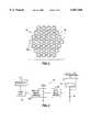
- FIG. 1is a top plan view of a fingerprint sensor in accordance with the present invention.
- FIG. 2is a schematic view of a circuit portion of the fingerprint sensor as shown in FIG. 1.
- FIG. 3is a greatly enlarged top plan view of the sensing portion of the fingerprint sensor as shown in FIG. 1.
- FIG. 4is a schematic diagram of another circuit portion of the fingerprint sensor as shown in FIG. 1.
- FIG. 5is a greatly enlarged side cross-sectional view of a portion of the fingerprint sensor as shown in FIG. 1.
- FIG. 6is a greatly enlarged side cross-sectional view of a portion of an alternate embodiment of the fingerprint sensor in accordance with the invention.
- FIG. 7is a greatly enlarged side cross-sectional view of another portion of the fingerprint sensor as shown in FIG. 1.
- FIG. 8is a schematic block diagram of yet another circuit portion of the fingerprint sensor as shown in FIG. 1.
- FIG. 9is a schematic circuit diagram of a portion of the circuit as shown in FIG. 8.
- FIG. 10is a schematic block diagram of still another circuit portion of the fingerprint sensor as shown in FIG. 1.
- FIG. 11is a schematic block diagram of an alternate embodiment of the circuit portion shown in FIG. 10.
- FIG. 12is a schematic block diagram of an additional circuit portion of the fingerprint sensor as shown in FIG. 1.
- FIG. 13is a schematic block diagram of an alternate embodiment of the circuit portion shown in FIG. 12.
- the illustrated sensor 30includes a housing or package 51, a dielectric layer 52 exposed on an upper surface of the package which provides a placement surface for the finger, and a plurality of output pins, not shown.
- a first conductive strip or external electrode 54 around the periphery of the dielectric layer 52, and a second external electrode 53provide contact electrodes for the finger 79 as described in greater detail below.
- the sensor 30may provide output signals in a range of sophistication levels depending on the level of processing incorporated in the package as would be readily understood by those skilled in the art.
- the sensor 30includes a plurality of individual pixels or sensing elements 30a arranged in array pattern as perhaps best shown in FIG. 3. As would be readily understood by those skilled in the art, these sensing elements are relatively small so as to be capable of sensing the ridges 59 and intervening valleys 60 of a typical fingerprint. As will also be readily appreciated by those skilled in the art, live fingerprint readings as from the electric field sensor 30 in accordance with the present invention may be more reliable than optical sensing, because the impedance of the skin of a finger in a pattern of ridges and valleys is extremely difficult to simulate. In contrast, an optical sensor may be deceived by a readily deceived by a photograph or other similar image of a fingerprint, for example.
- the sensor 30includes a substrate 65, and one or more active semiconductor devices formed thereon, such as the schematically illustrated amplifier 73.
- a first metal layer 66interconnects the active semiconductor devices.
- a second or ground plane electrode layer 68is above the first metal layer 66 and separated therefrom by an insulating layer 67.
- a third metal layer 71is positioned over another dielectric layer 70.
- the first external electrode 54is connected to an excitation drive amplifier 74 which, in turn, drives the finger 79 with a signal may be typically in the range of about 1 KHz to 1 MHz. Accordingly, the drive or excitation electronics are thus relatively uncomplicated and the overall cost of the sensor 30 may be relatively low, while the reliability is great.
- An illustratively circularly shaped electric field sensing electrode 78is on the insulating layer 70.
- the sensing electrode 78may be connected to sensing integrated electronics, such as the illustrated amplifier 73 formed adjacent the substrate 65 as schematically illustrated, and as would be readily appreciated by those skilled in the art.
- An annularly shaped shield electrode 80surrounds the sensing electrode 78 in spaced relation therefrom.
- the sensing electrode 78 and its surrounding shield electrode 80may have other shapes, such as hexagonal, for example, to facilitate a close packed arrangement or array of pixels or sensing elements 30a.
- the shield electrode 80is an active shield which is driven by a portion of the output of the amplifier 73 to help focus the electric field energy and, moreover, to thereby reduce the need to drive adjacent electric field sensing electrodes 78.
- the sensor 30includes only three metal or electrically conductive layers 66, 68 and 71.
- the sensor 30can be made without requiring additional metal layers which would otherwise increase the manufacturing cost, and, perhaps, reduce yields. Accordingly, the sensor 30 is less expensive and may be more rugged and reliable than a sensor including four or more metal layers as would be appreciated by those skilled in the art.
- the amplifier 73may be operated at a gain of greater than about one to drive the shield electrode 80. Stability problems do not adversely affect the operation of the amplifier 73. Moreover, the common mode and general noise rejection are greatly enhanced according to this feature of the invention. In addition, the gain greater than one tends to focus the electric field with resect to the sensing electrode 78 as will be readily appreciated by those skilled in the art.
- the sensing elements 30aoperate at very low currents and at very high impedances.
- the output signal from each sensing electrode 78is desirably about 5 to 10 millivolts to reduce the effects of noise and permit further processing of the signals.
- the approximate diameter of each sensing element 30a, as defined by the outer dimensions of the shield electrode 80,may be about 0.002 to 0.005 inches in diameter.
- the ground plane electrode 68protects the active electronic devices from unwanted excitation.
- the various signal feedthrough conductors for the electrodes 78, 80 to the active electronic circuitrymay be readily formed as would be understood by those skilled in the art.
- the overall contact or sensing surface for the sensor 30may desirably be about 0.5 by 0.5 inches--a size which may be readily manufactured and still provide a sufficiently large surface for accurate fingerprint sensing and identification.
- the sensor 30 in accordance with the inventionis also fairly tolerant of dead pixels or sensing elements 30a.
- a typical sensor 30includes an array of about 256 by 256 pixels or sensor elements, although other array sizes are also contemplated by the present invention.
- the sensor 30may also be fabricated at one time using primarily conventional semiconductor manufacturing techniques to thereby significantly reduce the manufacturing costs.
- the sensormay include power control means for controlling operation of active circuit portions 100 based upon sensing finger contact with the first external electrode 54 as determined by the illustrated finger sense block or circuit 101.
- the finger sense circuit 101may operate based upon a change in impedance to an oscillator to thereby determine finger contact.
- the power control meansmay include wake-up means for only powering active circuit portions upon sensing finger contact with the first external electrode to thereby conserve power.
- the power control meansmay further comprise protection means for grounding active circuit portions upon not sensing finger contact with the first external electrode. In the illustrated embodiment, a combination of wake-up and protection controller circuits 101 are illustrated.
- the fingerprint sensor 30may further comprise finger charge bleed means for bleeding a charge from a finger or other object upon contact therewith.
- the finger charge bleed meansmay be provided by the second external electrode 53 carried by the package 51 for contact by a finger, and a charge bleed resistor 104 connected between the second external electrode and an earth ground.
- the second electrodemay alternately be provided by a movable electrically conductive cover 53' slidably connected to the package 51 for covering the opening to the exposed upper dielectric layer 52.
- a pivotally connected coveris also contemplated by the present invention. Accordingly, under normal conditions, the charge would be bled from the finger as the cover 53' is moved to expose the sensing portion of the sensor 30.
- the finger charge bleed means and power control meansmay be such that the active portions remain grounded until the charge bleed means can remove the charge on the finger before powering the active circuit portions, such as by providing a brief delay during wake-up sufficient to permit the charge to be discharged through the resistor 104 as would be readily understood by those skilled in the art. Accordingly, power may be conserved in the sensor 30 and ESD protection provided by the sensor so that the sensor is relatively inexpensive, yet robust and conserves power.
- the dielectric covering 52may preferably comprise a z-axis anisotropic dielectric layer 110 for focussing an electric field, shown by the illustrated field lines, at each of the electric field sensing electrodes 78.
- the dielectric layer 110may be relatively thick, but not result in defocussing of the electric fields propagating therethrough because of the z-axis anisotropy of the material.
- a thin film which is desirable for focussingmay permit the underlying circuit to be more easily subject to damage.
- the z-axis anisotropic dielectric layer 110 of the present inventionmay have a thickness in range of about 0.0001 to 0.004 inches.
- the z-axis anisotropic dielectric layer 110is also preferably chemically resistant and mechanically strong to withstand contact with fingers, and to permit periodic cleanings with solvents.
- the z-axis anisotropic dielectric layer 110may preferably define an outermost protective surface for the integrated circuit die 120.
- the overall dielectric covering 52may further include at least one relatively thin oxide, nitride, carbide, or diamond layer 111 on the integrated circuit die 120 and beneath the z-axis anisotropic dielectric layer 110.
- the thin layer 111will typically be relatively hard, and the z-axis anisotropic dielectric layer 110 is desirably softer to thereby absorb more mechanical activity.
- the z-axis anisotropic dielectric layer 110may be provided by a plurality of oriented dielectric particles in a cured matrix.
- the z-axis anisotropic dielectric layer 110may comprise barium titanate in a polyimide matrix.
- materials exhibiting z-axis anisotropy suitable for the present inventionFor example, certain ceramics exhibit dielectric anisotropy as would also be appreciated by those skilled in the art.
- FIG. 6another variation of a z-axis dielectric covering 52' is schematically shown by a plurality of high dielectric portions 112 aligned with corresponding electric field sensing electrodes 78, and a surrounding matrix of lower dielectric portions 113.
- This embodiment of the dielectric covering 52'may be formed in a number of ways, such as by forming a layer of either the high dielectric or low dielectric portions, selectively etching same, and filling the openings with the opposite material.
- Another approachmay be to use polarizable microcapsules and subjecting same to an electric field during curing of a matrix material. A material may be compressed to cause the z-axis anisotropy. Laser and other selective processing techniques may also be used as would be readily understood by those skilled in the art.
- the third metal layer 71(FIG. 2) preferably further includes a plurality of capacitive coupling pads 116a-118a for permitting capacitive coupling of the integrated circuit die 120.
- the dielectric covering 52is preferably continuous over the capacitive coupling pads 116a-118a and the array of electric field sensing electrodes 78 of the pixels 30a (FIG. 1).
- itis conventional to create openings through an outer coating to electrically connect to the bond pads. Unfortunately, these openings would provide pathways for water and/or other contaminants to come in contact with and damage the die.
- a portion of the package 51includes a printed circuit board 122 which carries corresponding pads 115b-118b.
- a power modulation circuit 124is coupled to pads 115b-116b, while a signal modulation circuit 126 is illustrative coupled to pads 117b-118b.
- both power and signalsmay be readily coupled between the printed circuit board 122 and the integrated circuit die 120, further using the illustrated power demodulation/regulator circuit 127, and the signal demodulation circuit 128.
- the z-axis anisotropic dielectric layer 110also advantageously reduces cross-talk between adjacent capacitive coupling pads.
- This embodiment of the invention 30presents no penetrations through the dielectric covering 52 for moisture to enter and damage the integrated circuit die 120.
- another level of insulationis provided between the integrated circuit and the external environment.
- the package 51preferably has an opening aligned with the array of electric field sensing electrodes 78 (FIGS. 1-3).
- the capacitive coupling and z-axis anisotropic layer 110may be advantageously used in a number of applications in addition to the illustrated fingerprint sensor 30, and particularly where it is desired to have a continuous film covering the upper surface of the integrated circuit die 120 and pads 116a-118a.
- the fingerprint sensor 30may be considered as comprising an array of fingerprint sensing elements 130 and associated active circuits 131 for generating signals relating to the fingerprint image.
- the illustrated sensor 30also includes an impedance matrix 135 connected to the active circuits for filtering the signals therefrom.
- the impedance matrix 135includes a plurality of impedance elements 136 with a respective impedance element connectable between each active circuit of a respective fingerprint sensing element as indicated by the central node 138, and the other active circuits (outer nodes 140).
- the impedance matrix 135also includes a plurality of switches 137 with a respective switch connected in series with each impedance element 136.
- An input signalmay be supplied to the central node 138 via the illustrated switch 142 and its associated impedance element 143.
- the impedance elementmay one or more of a resistor as illustrated, and a capacitor 134 as would be readily appreciated by those skilled in the art.
- Filter control meansmay operate the switches 137 to perform processing of the signals generated by the active circuits 131.
- the fingerprint sensing elements 130may be electric field sensing electrodes 78, and the active circuits 131 may be amplifiers 73 (FIG. 2).
- the active circuits 131may be amplifiers 73 (FIG. 2).
- Ridge flow determining means 145may be provided for selectively operating the switches 137 of the matrix 135 to determine ridge flow directions of the fingerprint image. More particularly, the ridge flow determining means 145 may selectively operate the switches 137 for determining signal strength vectors relating to ridge flow directions of the fingerprint image. As would be readily understood by those skilled in the art, the ridge flow directions may be determined based upon well known rotating slit principles.
- the sensor 30may include core location determining means 146 cooperating with the ridge flow determining means 145 for determining a core location of the fingerprint image.
- the position of the coreis helpful, for example, in extracting and processing minutiae from the fingerprint image as would also be readily understood by those skilled in the art.
- a binarizing filter 150may be provided for selectively operating the switches 137 to convert a gray scale fingerprint image to a binarized fingerprint image.
- the impedance matrix 135may be used to provide dynamic image contrast enhancement.
- an edge smoothing filter 155may be readily implemented to improve the image.
- other spatial filters 152may also be implemented using the impedance matrix 135 for selectively operating the switches 137 to spatially filter the fingerprint image as would be readily appreciated by those of skill in the art. Accordingly, processing of the fingerprint image may be carried out at the sensor 30 and thereby reduce additional downstream computational requirements.
- the impedance matrix 135may comprise a plurality of impedance elements with a respective impedance element 136 connectable between each active circuit for a given fingerprint sensing element 130 and eight other active circuits for respective adjacent fingerprint sensing elements.
- control means 153for sequentially powering sets of active circuits 131 to thereby conserve power.
- the respective impedance elements 136are desirably also sequentially connected to perform the filtering function.
- the powered active circuits 131may be considered as defining a cloud or kernel as would be readily appreciated by those skilled in the art.
- the power control means 153may be operated in an adaptive fashion whereby the size of the area used for filtering is dynamically changed for preferred image characteristics as would also be readily understood by those skilled in the art.
- the power control means 153may also power only certain ones of the active circuits corresponding to a predetermined area of the array of sensing elements 130. For example, every other active circuit 131 could be powered to thereby provide a larger area, but reduced power consumption as would also be understood by those skilled in the art.
- Reader control means 154may be provided to read only predetermined subsets of each set of active circuits 131 so that a contribution from adjacent active circuits is used for filtering.
- only a subset of active circuits 131are typically simultaneously read although adjacent active circuits 131 and associated impedance elements 136 are also powered and connected, respectively.
- 16 impedance elements 136could define a subset and be readily simultaneously read.
- the subset sizecould be optimized for different sized features to be determined as would be readily appreciated by those skilled in the art.
- the array of sense elements 130can be quickly read, and power consumption substantially reduced since all of the active circuits 131 need not be powered for reading a given set of active circuits.
- the combination of the power control and impedance matrix features described hereinmay permit power savings by a factor of about 10 as compared to powering the full array.
- the fingerprint sensor 30It is another important advantage of the fingerprint sensor 30 according to present invention to guard against spoofing or deception of the sensor into incorrectly treating a simulated image as a live fingerprint image.
- optical sensorsmay be deceived or spoofed by using a paper with a fingerprint image thereon.
- the unique electric field sensing of the fingerprint sensor 30 of the present inventionprovides an effective approach to avoiding spoofing based upon the complex impedance of a finger.
- the fingerprint sensor 30may be considered as including an array of impedance sensing elements 160 for generating signals related to a finger 79 or other object positioned adjacent thereto.
- the impedance sensing elements 160are provided by electric field sensing electrodes 78 and amplifiers 73 (FIG. 2) associated therewith.
- a guard shield 80may be associated with each electric field sensing electrode 78 and connected to a respective amplifier 73.
- Spoof reducing means 161is provided for determining whether or not an impedance of the object positioned adjacent the array of impedance sensing elements 160 corresponds to a live finger 79 to thereby reduce spoofing of the fingerprint sensor by an object other than a live finger.
- a spoofingmay be indicated, such as by the schematically illustrated lamp 163 and/or used to block further processing.
- a live fingerprint determinationmay also be indicated by a lamp 164 and/or used to permit further processing of the fingerprint image as will be readily appreciated by those skilled in the art.
- Many other options for indicating a live fingerprint or an attempted spoofingwill be readily appreciated by those skilled in the art.
- the spoof reducing means 161may include impedance determining means 165 to detect a complex impedance having a phase angle in a range of about 10 to 60 degrees corresponding to a live finger 79.
- the spoof reducing means 161may detect an impedance having a phase angle of about 0 degrees corresponding to some objects other than a live finger, such as a sheet of paper having an image thereon, for example.
- the spoof reducing means 161may detect an impedance of 90 degrees corresponding to other objects.
- the fingerprint sensor 30may preferably includes drive means for driving the array of impedance sensing elements 160, such as the illustrated excitation amplifier 74 (FIG. 2).
- the sensoralso includes synchronous demodulator means 170 for synchronously demodulating signals from the array of impedance sensing elements 160.
- the spoof reducing meanscomprises means for operating the synchronous demodulator means 170 at at least one predetermined phase rotation angle.
- the synchronous demodulator means 170could be operated in a range of about 10 to 60 degrees, and the magnitude compared to a predetermined threshold indicative of a live fingerprint.
- a live fingerprinttypically has a complex impedance within the range of 10 to 60 degrees.
- ratio generating and comparing means 172may be provided for cooperating with the synchronous demodulator means 170 for synchronously demodulating signals at first and second phase angles ⁇ 1 , ⁇ 2 , generating an amplitude ratio thereof, and comparing the amplitude ratio to a predetermined threshold to determine whether the object is a live fingerprint or other object.
- the synchronous demodulator 170may be readily used to generate the impedance information desired for reducing spoofing of the sensor 30 by an object other than a live finger.
- the first angle ⁇ 1 and the second 92may have a difference in a range of about 45 to 90 degrees, for example. Other angles are also contemplated by the invention as would be readily appreciated by those skilled in the art.
- the fingerprint sensor 30also includes an automatic gain control feature to account for a difference in intensity of the image signals generated by different fingers or under different conditions, and also to account for differences in sensor caused by process variations. It is important for accurately producing a fingerprint image, that the sensor can discriminate between the ridges and valleys of the fingerprint. Accordingly, the sensor 30 includes a gain control feature, a first embodiment of which is understood with reference to FIG. 12.
- the illustrated portion of the fingerprint sensor 30includes an array of fingerprint sensing elements in the form of the electric field sensing electrodes 78 and surrounding shield electrodes 80 connected to the amplifiers 73.
- Other fingerprint sensing elementsmay also benefit from the following automatic gain control implementations as will be appreciated by those skilled in the art.
- the signal processing circuitry of the sensor 30preferably includes a plurality of analog-to-digital (A/D) converters 180 as illustrated. Moreover, each of these A/D converters 180 may have a controllable scale. Scanning means 182 sequentially connects different elements to the bank of A/D converters 180.
- the illustrated gain processor 185provides range determining and setting means for controlling the range of the A/D converters 180 based upon prior A/D conversions to thereby provide enhanced conversion resolution.
- the A/D converters 180may comprise the illustrated reference voltage input Vref and offset voltage input V offset for permitting setting of the range as would be readily appreciated by those skilled in the at.
- the range determining and setting meansmay also comprise a first digital-to-analog D/A converter 186 connected between the gain processor 185 and the reference voltage Vref inputs of the A/D converters 180 as would also be readily understood by those skilled in the art.
- a second D/A converter 189is also illustratively connected to the offset voltage inputs V offset from the gain processor 185.
- the gain processor 185may comprise histogram generating means for generating a histogram, as described above, and based upon prior A/D conversions.
- the graph adjacent the gain processor 185 in FIG. 12illustrates a typical histogram plot 191.
- the histogram plot 191includes two peaks corresponding to the sensed ridges and valleys of the fingerprint as would be readily appreciated by those skilled in the art. By setting the range for the A/D converters 180, the peaks can be readily positioned as desired to thereby account for the variations discussed above and use the full resolution of the A/D converters 180.
- the A/D converters 180may include an associated input amplifier for permitting setting of the range.
- the range determining and setting meansmay also comprise the illustrated gain processor 185, and wherein the amplifier is a programmable gain amplifier (PGA) 187 connected to the processor.
- PGAprogrammable gain amplifier
- a digital word output from the gain processor 185sets the gain of the PGA 187 so that full use of the resolution of the A/D converters 180 is obtained for best accuracy.
- a second digital word output from the gain processor 185 and coupled to the amplifier 187 through the illustrated D/A converter 192may also control the offset of the amplifier as would also be readily appreciated by those skilled in the art.
- the range determining and setting means of the gain processor 185may comprise default setting means for setting a default range for initial ones of the fingerprint sensing elements.
- the automatic gain control feature of the present inventionallows the D/A converters 180 to operate over their full resolution range to thereby increase the accuracy of the image signal processing.
Landscapes
- Engineering & Computer Science (AREA)
- Physics & Mathematics (AREA)
- General Physics & Mathematics (AREA)
- Multimedia (AREA)
- Theoretical Computer Science (AREA)
- Human Computer Interaction (AREA)
- Computer Vision & Pattern Recognition (AREA)
- Image Input (AREA)
- Measurement Of Length, Angles, Or The Like Using Electric Or Magnetic Means (AREA)
- Measurement Of The Respiration, Hearing Ability, Form, And Blood Characteristics Of Living Organisms (AREA)
Abstract
Description
The present application is a continuation-in-part of application Ser. No. 08/590,564, now U.S. Pat. No. 5,828,773, filed Jan. 26, 1996.
The present invention relates to the field of personal identification and verification, and, more particularly, to the field of fingerprint sensing and processing.
Fingerprint sensing and matching is a reliable and widely used technique for personal identification or verification. In particular, a common approach to fingerprint identification involves scanning a sample fingerprint or an image thereof and storing the image and/or unique characteristics of the fingerprint image. The characteristics of a sample fingerprint may be compared to information for reference fingerprints already in a database to determine proper identification of a person, such as for verification purposes.
A typical electronic fingerprint sensor is based upon illuminating the finger surface using visible light, infrared light, or ultrasonic radiation. The reflected energy is captured with some form of camera, for example, and the resulting image is framed, digitized and stored as a static digital image. For example, U.S. Pat. No. 4,210,899 to Swonger et al. discloses an optical scanning fingerprint reader cooperating with a central processing station for a secure access application, such as admitting a person to a location or providing access to a computer terminal. U.S. Pat. No. 4,525,859 to Bowles similarly discloses a video camera for capturing a fingerprint image and uses the minutiae of the fingerprints, that is, the branches and endings of the fingerprint ridges, to determine a match with a database of reference fingerprints.
Unfortunately, optical sensing may be affected by stained fingers or an optical sensor may be deceived by presentation of a photograph or printed image of a fingerprint rather than a true live fingerprint. In addition, optical schemes may require relatively large spacings between the finger contact surface and associated imaging components. Moreover, such sensors typically require precise alignment and complex scanning of optical beams. Accordingly, optical sensors may thus be bulky and be susceptible to shock, vibration and surface contamination. Accordingly, an optical fingerprint sensor may be unreliable in service in addition to being bulky and relatively expensive due to optics and moving parts.
U.S. Pat. No. 4,353,056 to Tsikos discloses another approach to sensing a live fingerprint. In particular, the patent discloses an array of extremely small capacitors located in a plane parallel to the sensing surface of the device. When a finger touches the sensing surface and deforms the surface, a voltage distribution in a series connection of the capacitors may change. The voltages on each of the capacitors is determined by multiplexor techniques. Unfortunately, the resilient materials required for the sensor may suffer from long term reliability problems. In addition, multiplexing techniques for driving and scanning each of the individual capacitors may be relatively slow and cumbersome. Moreover, noise and stray capacitances may adversely affect the plurality of relatively small and closely spaced capacitors.
U.S. Pat. No. 5,325,442 to Knapp discloses a fingerprint sensor including a plurality of sensing electrodes. Active addressing of the sensing electrodes is made possible by the provision of a switching device associated with each sensing electrode. A capacitor is effectively formed by each sensing electrode in combination with the respective overlying portion of the finger surface which, in turn, is at ground potential. The sensor may be fabricated using semiconductor wafer and integrated circuit technology. The dielectric material upon which the finger is placed may be provided by silicon nitride or a polyimide which may be provided as a continuous layer over an array of sensing electrodes. Further conductors may be provided on the surface of the dielectric material remote from the sensing electrodes and extending over regions between the sensing electrodes, for example, as lines or in grid form, which conductors are grounded in order to improve the electrical contact to the finger surface.
Unfortunately, driving the array of closely spaced sensing electrodes as disclosed in the Knapp et al. patent may be difficult since adjacent electrodes may affect one another. Another difficulty with such a sensor may be its ability to distinguish ridges and valleys of a fingerprint when the conductivity of the skin and any contaminants may vary widely from person-to-person and even over a single fingerprint. Yet another difficulty with such a sensor, as with many optical sensors, is that different portions of the fingerprint may require relatively complicated post image collection processing to provide for usable signal levels and contrast to thereby permit accurate determination of the ridges and valleys of the fingerprint. For example, U.S. Pat. No. 4,811,414 to Fishbine et al. discloses methods for noise averaging, illumination equalizing, directional filtering, curvature correcting, and scale correcting for an optically generated fingerprint image. Unfortunately, the various processing steps are complex and require considerable computational power in a downstream processor. Signal processing of other fingerprint circuits may also be relatively complicated and therefore expensive and/or slow.
Greater advances in fingerprint sensing and matching for identification and verification are desirable for many applications. Unfortunately, current sensors and their associated circuitry may be too bulky, expensive and unreliable for a great many applications which would otherwise benefit from fingerprint identification and verification technology. In addition, conventional fingerprint sensors may be require considerable downstream processing of image signals and/or be slow to process the image. Moreover, conventional fingerprint sensors may consume relatively large amounts of power, thereby further limiting the number of potential applications.
In view of the foregoing background, it is therefore an object of the present invention to provide a fingerprint sensor and associated methods for generating and processing the fingerprint image without requiring substantial computing power, and while conserving electrical power.
This and other objects, features, and advantages according to the invention are provided by a fingerprint sensor comprising an array of fingerprint sensing elements and associated active circuits for generating signals relating to the fingerprint image, and impedance matrix filtering means connected to the active circuits for filtering the signals. The impedance matrix filtering means preferably comprises a plurality of impedance elements with a respective impedance element connectable between each active circuit of a respective fingerprint sensing element and at least one other active circuit for a respective at least one adjacent fingerprint sensing element. The impedance matrix filtering means may also include a plurality of switches with a respective switch connected in series with each impedance element. Filter control means may operate the switches to perform processing of the signals generated by the active circuits. In one embodiment, the fingerprint sensing elements may be electric field sensing electrodes, and the active circuits may be amplifiers.
Ridge flow determining means may be provided for selectively operating the switches to determine ridge flow directions of the fingerprint image. More particularly, the ridge flow determining means may selectively operate the switches for determining signal strength vectors relating to ridge flow directions of the fingerprint image. In addition, the sensor may include core location determining means cooperating with the ridge flow determining means for determining a core location of the fingerprint image.
According to another aspect of the invention, binarizing filter means may be provided for selectively operating the switches to convert a gray scale fingerprint image to a binarized fingerprint image. Considered another way, the impedance matrix may be used to provide dynamic image contrast enhancement. Edge smoothing may also be implemented using the impedance matrix. Other spatial filters may also be implemented for selectively operating the switches to spatially filter the fingerprint image. Accordingly, processing of the fingerprint image may be carried out at the sensor and thereby reduce additional downstream computational requirements.
The impedance matrix filtering means may comprise a plurality of impedance elements with a respective impedance element connectable between each active circuit for a given fingerprint sensing element and eight other active circuits for respective adjacent fingerprint sensing elements. The impedance elements may be resistors or capacitors, for example.
Yet another aspect of the invention is the provision of control means for sequentially powering sets of active circuits to thereby conserve power and perform filtering. In other words, the respective impedance elements may also be sequentially connected to perform the filtering function. The power control means may further comprise adaptive means for changing a number of active circuits in a set of active circuits being powered. In addition, the power control means may further comprise means for powering only predetermined ones of the active circuits in a set of active circuits defined by respective fingerprint sensing elements in the predetermined area to thereby further conserve power while performing filtering. Reader control means may be provided to read only predetermined subsets of each set of active circuits so that a contribution from adjacent active circuits is used for filtering, but other portions are not unnecessarily powered.
One method aspect of the invention is for making a fingerprint sensor. The method preferably comprises the steps of: forming an array of fingerprint sensing elements and associated active circuits, and forming a plurality of impedance elements so that a respective impedance element is selectably connectable between each active circuit for a respective fingerprint sensing element and at least one other active circuit for at least one other respective adjacent fingerprint sensing element to generate signals relating to a fingerprint.
Another method aspect of the invention is for sensing a fingerprint image using a sensor of a type comprising a plurality fingerprint sensing elements and associated active circuits, and an impedance matrix filter connected to the active circuits. This method preferably comprises the steps of: generating fingerprint image signals from the active circuits, and determining ridge flow directions in the fingerprint using the impedance matrix filter. The method may also further include the step of determining a core location of the fingerprint image based on the ridge flow directions.
Yet another method aspect of the invention is for sensing a fingerprint image using a sensor as described above. This method preferably comprises the steps of: generating fingerprint image signals from the active circuits; and converting a gray scale fingerprint image to a binarized fingerprint image using the impedance matrix filter. Still another method uses the impedance matrix to perform edge smoothing.
FIG. 1 is a top plan view of a fingerprint sensor in accordance with the present invention.
FIG. 2 is a schematic view of a circuit portion of the fingerprint sensor as shown in FIG. 1.
FIG. 3 is a greatly enlarged top plan view of the sensing portion of the fingerprint sensor as shown in FIG. 1.
FIG. 4 is a schematic diagram of another circuit portion of the fingerprint sensor as shown in FIG. 1.
FIG. 5 is a greatly enlarged side cross-sectional view of a portion of the fingerprint sensor as shown in FIG. 1.
FIG. 6 is a greatly enlarged side cross-sectional view of a portion of an alternate embodiment of the fingerprint sensor in accordance with the invention.
FIG. 7 is a greatly enlarged side cross-sectional view of another portion of the fingerprint sensor as shown in FIG. 1.
FIG. 8 is a schematic block diagram of yet another circuit portion of the fingerprint sensor as shown in FIG. 1.
FIG. 9 is a schematic circuit diagram of a portion of the circuit as shown in FIG. 8.
FIG. 10 is a schematic block diagram of still another circuit portion of the fingerprint sensor as shown in FIG. 1.
FIG. 11 is a schematic block diagram of an alternate embodiment of the circuit portion shown in FIG. 10.
FIG. 12 is a schematic block diagram of an additional circuit portion of the fingerprint sensor as shown in FIG. 1.
FIG. 13 is a schematic block diagram of an alternate embodiment of the circuit portion shown in FIG. 12.
The present invention will now be described more fully hereinafter with reference to the accompanying drawings, in which preferred embodiments of the invention are shown. This invention may, however, be embodied in many different forms and should not be construed as limited to the embodiments set forth herein. Rather, these embodiments are provided so that this disclosure will be thorough and complete, and will fully convey the scope of the invention to those skilled in the art. Like numbers refer to like elements throughout. The scaling of various features, particularly layers in the drawing figures, have been exaggerated for clarity of explanation.
Referring to FIGS. 1-3, thefingerprint sensor 30 in accordance with the invention is initially described. The illustratedsensor 30 includes a housing orpackage 51, adielectric layer 52 exposed on an upper surface of the package which provides a placement surface for the finger, and a plurality of output pins, not shown. A first conductive strip orexternal electrode 54 around the periphery of thedielectric layer 52, and a secondexternal electrode 53 provide contact electrodes for thefinger 79 as described in greater detail below. Thesensor 30 may provide output signals in a range of sophistication levels depending on the level of processing incorporated in the package as would be readily understood by those skilled in the art.
Thesensor 30 includes a plurality of individual pixels orsensing elements 30a arranged in array pattern as perhaps best shown in FIG. 3. As would be readily understood by those skilled in the art, these sensing elements are relatively small so as to be capable of sensing the ridges 59 and intervening valleys 60 of a typical fingerprint. As will also be readily appreciated by those skilled in the art, live fingerprint readings as from theelectric field sensor 30 in accordance with the present invention may be more reliable than optical sensing, because the impedance of the skin of a finger in a pattern of ridges and valleys is extremely difficult to simulate. In contrast, an optical sensor may be deceived by a readily deceived by a photograph or other similar image of a fingerprint, for example.
Thesensor 30 includes asubstrate 65, and one or more active semiconductor devices formed thereon, such as the schematically illustratedamplifier 73. A first metal layer 66 interconnects the active semiconductor devices. A second or groundplane electrode layer 68 is above the first metal layer 66 and separated therefrom by an insulatinglayer 67. Athird metal layer 71 is positioned over anotherdielectric layer 70. In the illustrated embodiment, the firstexternal electrode 54 is connected to anexcitation drive amplifier 74 which, in turn, drives thefinger 79 with a signal may be typically in the range of about 1 KHz to 1 MHz. Accordingly, the drive or excitation electronics are thus relatively uncomplicated and the overall cost of thesensor 30 may be relatively low, while the reliability is great.
An illustratively circularly shaped electricfield sensing electrode 78 is on the insulatinglayer 70. Thesensing electrode 78 may be connected to sensing integrated electronics, such as the illustratedamplifier 73 formed adjacent thesubstrate 65 as schematically illustrated, and as would be readily appreciated by those skilled in the art.
An annularly shapedshield electrode 80 surrounds thesensing electrode 78 in spaced relation therefrom. As would be readily appreciated by those skilled in the art, thesensing electrode 78 and its surroundingshield electrode 80 may have other shapes, such as hexagonal, for example, to facilitate a close packed arrangement or array of pixels orsensing elements 30a. Theshield electrode 80 is an active shield which is driven by a portion of the output of theamplifier 73 to help focus the electric field energy and, moreover, to thereby reduce the need to drive adjacent electricfield sensing electrodes 78.
Thesensor 30 includes only three metal or electricallyconductive layers sensor 30 can be made without requiring additional metal layers which would otherwise increase the manufacturing cost, and, perhaps, reduce yields. Accordingly, thesensor 30 is less expensive and may be more rugged and reliable than a sensor including four or more metal layers as would be appreciated by those skilled in the art.
Another important aspect of the present invention is that theamplifier 73 may be operated at a gain of greater than about one to drive theshield electrode 80. Stability problems do not adversely affect the operation of theamplifier 73. Moreover, the common mode and general noise rejection are greatly enhanced according to this feature of the invention. In addition, the gain greater than one tends to focus the electric field with resect to thesensing electrode 78 as will be readily appreciated by those skilled in the art.
In general, thesensing elements 30a operate at very low currents and at very high impedances. For example, the output signal from each sensingelectrode 78 is desirably about 5 to 10 millivolts to reduce the effects of noise and permit further processing of the signals. The approximate diameter of eachsensing element 30a, as defined by the outer dimensions of theshield electrode 80, may be about 0.002 to 0.005 inches in diameter. Theground plane electrode 68 protects the active electronic devices from unwanted excitation. The various signal feedthrough conductors for theelectrodes
The overall contact or sensing surface for thesensor 30 may desirably be about 0.5 by 0.5 inches--a size which may be readily manufactured and still provide a sufficiently large surface for accurate fingerprint sensing and identification. Thesensor 30 in accordance with the invention is also fairly tolerant of dead pixels orsensing elements 30a. Atypical sensor 30 includes an array of about 256 by 256 pixels or sensor elements, although other array sizes are also contemplated by the present invention. Thesensor 30 may also be fabricated at one time using primarily conventional semiconductor manufacturing techniques to thereby significantly reduce the manufacturing costs.
Turning now additionally to FIG. 4, another aspect of thesensor 30 of the invention is described. The sensor may include power control means for controlling operation ofactive circuit portions 100 based upon sensing finger contact with the firstexternal electrode 54 as determined by the illustrated finger sense block orcircuit 101. For example, thefinger sense circuit 101 may operate based upon a change in impedance to an oscillator to thereby determine finger contact. Of course, other approaches for sensing contact with the finger are also contemplated by the invention. The power control means may include wake-up means for only powering active circuit portions upon sensing finger contact with the first external electrode to thereby conserve power. Alternately or additionally, the power control means may further comprise protection means for grounding active circuit portions upon not sensing finger contact with the first external electrode. In the illustrated embodiment, a combination of wake-up andprotection controller circuits 101 are illustrated.
Moreover, thefingerprint sensor 30 may further comprise finger charge bleed means for bleeding a charge from a finger or other object upon contact therewith. The finger charge bleed means may be provided by the secondexternal electrode 53 carried by thepackage 51 for contact by a finger, and acharge bleed resistor 104 connected between the second external electrode and an earth ground. As schematically illustrated in the upper right hand portion of FIG. 4, the second electrode may alternately be provided by a movable electrically conductive cover 53' slidably connected to thepackage 51 for covering the opening to the exposedupper dielectric layer 52. A pivotally connected cover is also contemplated by the present invention. Accordingly, under normal conditions, the charge would be bled from the finger as the cover 53' is moved to expose the sensing portion of thesensor 30.
In addition, the finger charge bleed means and power control means may be such that the active portions remain grounded until the charge bleed means can remove the charge on the finger before powering the active circuit portions, such as by providing a brief delay during wake-up sufficient to permit the charge to be discharged through theresistor 104 as would be readily understood by those skilled in the art. Accordingly, power may be conserved in thesensor 30 and ESD protection provided by the sensor so that the sensor is relatively inexpensive, yet robust and conserves power.
Referring now additionally to FIG. 5 yet another significant feature of thesensor 30 is described. Thedielectric covering 52 may preferably comprise a z-axis anisotropicdielectric layer 110 for focussing an electric field, shown by the illustrated field lines, at each of the electricfield sensing electrodes 78. In other words, thedielectric layer 110 may be relatively thick, but not result in defocussing of the electric fields propagating therethrough because of the z-axis anisotropy of the material. Typically there would be a trade-off between field focus and mechanical protection. Unfortunately, a thin film which is desirable for focussing, may permit the underlying circuit to be more easily subject to damage.
The z-axis anisotropicdielectric layer 110 of the present invention, for example, may have a thickness in range of about 0.0001 to 0.004 inches. Of course, the z-axis anisotropicdielectric layer 110 is also preferably chemically resistant and mechanically strong to withstand contact with fingers, and to permit periodic cleanings with solvents. The z-axis anisotropicdielectric layer 110 may preferably define an outermost protective surface for the integrated circuit die 120. Accordingly, the overall dielectric covering 52 may further include at least one relatively thin oxide, nitride, carbide, ordiamond layer 111 on the integrated circuit die 120 and beneath the z-axis anisotropicdielectric layer 110. Thethin layer 111 will typically be relatively hard, and the z-axis anisotropicdielectric layer 110 is desirably softer to thereby absorb more mechanical activity.
The z-axis anisotropicdielectric layer 110 may be provided by a plurality of oriented dielectric particles in a cured matrix. For example, the z-axis anisotropicdielectric layer 110 may comprise barium titanate in a polyimide matrix. Those of skill in the art will appreciate other materials exhibiting z-axis anisotropy suitable for the present invention. For example, certain ceramics exhibit dielectric anisotropy as would also be appreciated by those skilled in the art.
Turning to FIG. 6, another variation of a z-axis dielectric covering 52' is schematically shown by a plurality of highdielectric portions 112 aligned with corresponding electricfield sensing electrodes 78, and a surrounding matrix of lowerdielectric portions 113. This embodiment of the dielectric covering 52' may be formed in a number of ways, such as by forming a layer of either the high dielectric or low dielectric portions, selectively etching same, and filling the openings with the opposite material. Another approach may be to use polarizable microcapsules and subjecting same to an electric field during curing of a matrix material. A material may be compressed to cause the z-axis anisotropy. Laser and other selective processing techniques may also be used as would be readily understood by those skilled in the art.
Another aspect of the invention relates to being able to completely cover and protect the entire upper surface of the integrated circuit die 120, and still permit connection and communication with the external devices and circuits as now further explained with reference to FIG. 7. The third metal layer 71 (FIG. 2) preferably further includes a plurality ofcapacitive coupling pads 116a-118a for permitting capacitive coupling of the integrated circuit die 120. Accordingly, the dielectric covering 52 is preferably continuous over thecapacitive coupling pads 116a-118a and the array of electricfield sensing electrodes 78 of thepixels 30a (FIG. 1). In sharp contrast to this feature of the present invention, it is conventional to create openings through an outer coating to electrically connect to the bond pads. Unfortunately, these openings would provide pathways for water and/or other contaminants to come in contact with and damage the die.
A portion of thepackage 51 includes a printedcircuit board 122 which carries correspondingpads 115b-118b. Apower modulation circuit 124 is coupled topads 115b-116b, while asignal modulation circuit 126 is illustrative coupled topads 117b-118b. As would be readily understood by those skilled in the art, both power and signals may be readily coupled between the printedcircuit board 122 and the integrated circuit die 120, further using the illustrated power demodulation/regulator circuit 127, and thesignal demodulation circuit 128. The z-axis anisotropicdielectric layer 110 also advantageously reduces cross-talk between adjacent capacitive coupling pads. This embodiment of theinvention 30 presents no penetrations through the dielectric covering 52 for moisture to enter and damage the integrated circuit die 120. In addition, another level of insulation is provided between the integrated circuit and the external environment.
For the illustratedfingerprint sensor 30, thepackage 51 preferably has an opening aligned with the array of electric field sensing electrodes 78 (FIGS. 1-3). The capacitive coupling and z-axisanisotropic layer 110 may be advantageously used in a number of applications in addition to the illustratedfingerprint sensor 30, and particularly where it is desired to have a continuous film covering the upper surface of the integrated circuit die 120 andpads 116a-118a.
Further aspects of the manufacturing of thesensor 30 including the z-axis anisotropic dielectric material are explained in U.S. patent application, Ser. No. 08/857,525, filed May 16, 1997, entitled "Direct Chip Attachment Method and Devices Produced Thereby". This patent is assigned to the present assignee, and the entire disclosure of which is incorporated herein by reference.
Referring additionally to FIGS. 8 and 9, impedance matrix filtering aspects of the invention are now described. As shown in FIG. 8, thefingerprint sensor 30 may be considered as comprising an array offingerprint sensing elements 130 and associatedactive circuits 131 for generating signals relating to the fingerprint image. The illustratedsensor 30 also includes animpedance matrix 135 connected to the active circuits for filtering the signals therefrom.
As shown with more particular reference to FIG. 9, theimpedance matrix 135 includes a plurality ofimpedance elements 136 with a respective impedance element connectable between each active circuit of a respective fingerprint sensing element as indicated by thecentral node 138, and the other active circuits (outer nodes 140). Theimpedance matrix 135 also includes a plurality ofswitches 137 with a respective switch connected in series with eachimpedance element 136. An input signal may be supplied to thecentral node 138 via the illustratedswitch 142 and its associatedimpedance element 143. The impedance element may one or more of a resistor as illustrated, and acapacitor 134 as would be readily appreciated by those skilled in the art.
Filter control means may operate theswitches 137 to perform processing of the signals generated by theactive circuits 131. In one embodiment, thefingerprint sensing elements 130 may be electricfield sensing electrodes 78, and theactive circuits 131 may be amplifiers 73 (FIG. 2). Of course other sensing elements and active circuits may also benefit from the impedance matrix filtering of the present invention as would be readily understood by those skilled in the art.
Ridge flow determining means 145 may be provided for selectively operating theswitches 137 of thematrix 135 to determine ridge flow directions of the fingerprint image. More particularly, the ridge flow determining means 145 may selectively operate theswitches 137 for determining signal strength vectors relating to ridge flow directions of the fingerprint image. As would be readily understood by those skilled in the art, the ridge flow directions may be determined based upon well known rotating slit principles.
Thesensor 30 may include core location determining means 146 cooperating with the ridge flow determining means 145 for determining a core location of the fingerprint image. The position of the core is helpful, for example, in extracting and processing minutiae from the fingerprint image as would also be readily understood by those skilled in the art.
As also schematically illustrated in FIG. 8, abinarizing filter 150 may be provided for selectively operating theswitches 137 to convert a gray scale fingerprint image to a binarized fingerprint image. Considered another way, theimpedance matrix 135 may be used to provide dynamic image contrast enhancement. In addition, anedge smoothing filter 155 may be readily implemented to improve the image. As also schematically illustrated otherspatial filters 152 may also be implemented using theimpedance matrix 135 for selectively operating theswitches 137 to spatially filter the fingerprint image as would be readily appreciated by those of skill in the art. Accordingly, processing of the fingerprint image may be carried out at thesensor 30 and thereby reduce additional downstream computational requirements.
As shown in the illustrated embodiment of FIG. 9, theimpedance matrix 135 may comprise a plurality of impedance elements with arespective impedance element 136 connectable between each active circuit for a givenfingerprint sensing element 130 and eight other active circuits for respective adjacent fingerprint sensing elements.
Yet another aspect of the invention is the provision of control means 153 for sequentially powering sets ofactive circuits 131 to thereby conserve power. Of course, therespective impedance elements 136 are desirably also sequentially connected to perform the filtering function. The poweredactive circuits 131 may be considered as defining a cloud or kernel as would be readily appreciated by those skilled in the art. The power control means 153 may be operated in an adaptive fashion whereby the size of the area used for filtering is dynamically changed for preferred image characteristics as would also be readily understood by those skilled in the art. In addition, the power control means 153 may also power only certain ones of the active circuits corresponding to a predetermined area of the array of sensingelements 130. For example, every otheractive circuit 131 could be powered to thereby provide a larger area, but reduced power consumption as would also be understood by those skilled in the art.
Reader control means 154 may be provided to read only predetermined subsets of each set ofactive circuits 131 so that a contribution from adjacent active circuits is used for filtering. In other words, only a subset ofactive circuits 131 are typically simultaneously read although adjacentactive circuits 131 and associatedimpedance elements 136 are also powered and connected, respectively. For example, 16impedance elements 136 could define a subset and be readily simultaneously read. The subset size could be optimized for different sized features to be determined as would be readily appreciated by those skilled in the art.
Accordingly, the array ofsense elements 130 can be quickly read, and power consumption substantially reduced since all of theactive circuits 131 need not be powered for reading a given set of active circuits. For a typical sensor, the combination of the power control and impedance matrix features described herein may permit power savings by a factor of about 10 as compared to powering the full array.
It is another important advantage of thefingerprint sensor 30 according to present invention to guard against spoofing or deception of the sensor into incorrectly treating a simulated image as a live fingerprint image. For example, optical sensors may be deceived or spoofed by using a paper with a fingerprint image thereon. The unique electric field sensing of thefingerprint sensor 30 of the present invention provides an effective approach to avoiding spoofing based upon the complex impedance of a finger.
As shown in FIG. 10, thefingerprint sensor 30 may be considered as including an array ofimpedance sensing elements 160 for generating signals related to afinger 79 or other object positioned adjacent thereto. In the embodiment described herein, theimpedance sensing elements 160 are provided by electricfield sensing electrodes 78 and amplifiers 73 (FIG. 2) associated therewith. In addition, aguard shield 80 may be associated with each electricfield sensing electrode 78 and connected to arespective amplifier 73. Spoof reducing means 161 is provided for determining whether or not an impedance of the object positioned adjacent the array ofimpedance sensing elements 160 corresponds to alive finger 79 to thereby reduce spoofing of the fingerprint sensor by an object other than a live finger. A spoofing may be indicated, such as by the schematically illustratedlamp 163 and/or used to block further processing. Alternately, a live fingerprint determination may also be indicated by a lamp 164 and/or used to permit further processing of the fingerprint image as will be readily appreciated by those skilled in the art. Many other options for indicating a live fingerprint or an attempted spoofing will be readily appreciated by those skilled in the art.
In one embodiment, the spoof reducing means 161 may include impedance determining means 165 to detect a complex impedance having a phase angle in a range of about 10 to 60 degrees corresponding to alive finger 79. Alternately, the spoof reducing means 161 may detect an impedance having a phase angle of about 0 degrees corresponding to some objects other than a live finger, such as a sheet of paper having an image thereon, for example. In addition, the spoof reducing means 161 may detect an impedance of 90 degrees corresponding to other objects.
Turning now to FIG. 11, another embodiment of spoof reducing means is explained. Thefingerprint sensor 30 may preferably includes drive means for driving the array ofimpedance sensing elements 160, such as the illustrated excitation amplifier 74 (FIG. 2). The sensor also includes synchronous demodulator means 170 for synchronously demodulating signals from the array ofimpedance sensing elements 160. Accordingly, in one particularly advantageous embodiment of the invention, the spoof reducing means comprises means for operating the synchronous demodulator means 170 at at least one predetermined phase rotation angle. For example, the synchronous demodulator means 170 could be operated in a range of about 10 to 60 degrees, and the magnitude compared to a predetermined threshold indicative of a live fingerprint. A live fingerprint typically has a complex impedance within the range of 10 to 60 degrees.
Alternately, ratio generating and comparingmeans 172 may be provided for cooperating with the synchronous demodulator means 170 for synchronously demodulating signals at first and second phase angles θ1, θ2, generating an amplitude ratio thereof, and comparing the amplitude ratio to a predetermined threshold to determine whether the object is a live fingerprint or other object. Accordingly, thesynchronous demodulator 170 may be readily used to generate the impedance information desired for reducing spoofing of thesensor 30 by an object other than a live finger. The first angle θ1 and the second 92 may have a difference in a range of about 45 to 90 degrees, for example. Other angles are also contemplated by the invention as would be readily appreciated by those skilled in the art.
Thefingerprint sensor 30 also includes an automatic gain control feature to account for a difference in intensity of the image signals generated by different fingers or under different conditions, and also to account for differences in sensor caused by process variations. It is important for accurately producing a fingerprint image, that the sensor can discriminate between the ridges and valleys of the fingerprint. Accordingly, thesensor 30 includes a gain control feature, a first embodiment of which is understood with reference to FIG. 12.
As shown in FIG. 12, the illustrated portion of thefingerprint sensor 30 includes an array of fingerprint sensing elements in the form of the electricfield sensing electrodes 78 and surroundingshield electrodes 80 connected to theamplifiers 73. Other fingerprint sensing elements may also benefit from the following automatic gain control implementations as will be appreciated by those skilled in the art.
The signal processing circuitry of thesensor 30 preferably includes a plurality of analog-to-digital (A/D)converters 180 as illustrated. Moreover, each of these A/D converters 180 may have a controllable scale. Scanning means 182 sequentially connects different elements to the bank of A/D converters 180. The illustratedgain processor 185 provides range determining and setting means for controlling the range of the A/D converters 180 based upon prior A/D conversions to thereby provide enhanced conversion resolution. The A/D converters 180 may comprise the illustrated reference voltage input Vref and offset voltage input Voffset for permitting setting of the range as would be readily appreciated by those skilled in the at. Accordingly, the range determining and setting means may also comprise a first digital-to-analog D/A converter 186 connected between thegain processor 185 and the reference voltage Vref inputs of the A/D converters 180 as would also be readily understood by those skilled in the art. In addition, a second D/A converter 189 is also illustratively connected to the offset voltage inputs Voffset from thegain processor 185.
Thegain processor 185 may comprise histogram generating means for generating a histogram, as described above, and based upon prior A/D conversions. The graph adjacent thegain processor 185 in FIG. 12 illustrates atypical histogram plot 191. Thehistogram plot 191 includes two peaks corresponding to the sensed ridges and valleys of the fingerprint as would be readily appreciated by those skilled in the art. By setting the range for the A/D converters 180, the peaks can be readily positioned as desired to thereby account for the variations discussed above and use the full resolution of the A/D converters 180.
Turning additionally to FIG. 13, the A/D converters 180 may include an associated input amplifier for permitting setting of the range. In this variation, the range determining and setting means may also comprise the illustratedgain processor 185, and wherein the amplifier is a programmable gain amplifier (PGA) 187 connected to the processor. A digital word output from thegain processor 185 sets the gain of thePGA 187 so that full use of the resolution of the A/D converters 180 is obtained for best accuracy. A second digital word output from thegain processor 185 and coupled to theamplifier 187 through the illustrated D/A converter 192 may also control the offset of the amplifier as would also be readily appreciated by those skilled in the art.
The range determining and setting means of thegain processor 185 may comprise default setting means for setting a default range for initial ones of the fingerprint sensing elements. The automatic gain control feature of the present invention allows the D/A converters 180 to operate over their full resolution range to thereby increase the accuracy of the image signal processing.
Other aspects, advantages, and features relating to sensing of fingerprints are disclosed in copending U.S. patent application Ser. No. 08/592,469 entitled "Electric Field Fingerprint Sensor and Related Methods", and U.S. patent application Ser. No. 08/671,430 entitled "Integrated Circuit Device Having an Opening Exposing the Integrated Circuit Die and Related Methods", both assigned to the assignee of the present invention, and the entire disclosures of which are incorporated herein by reference. In addition, many modifications and other embodiments of the invention will come to the mind of one skilled in the art having the benefit of the teachings presented in the foregoing descriptions and the associated drawings. Therefore, it is to be understood that the invention is not to be limited to the specific embodiments disclosed, and that modifications and embodiments are intended to be included within the scope of the appended claims.
Claims (42)
1. A fingerprint sensor comprising:
an array of fingerprint sensing elements;
a plurality of active circuits with each active circuit connected to a respective fingerprint sensing element;
a plurality of impedance elements connected to said active circuits so that a respective impedance element is selectably connectable between each active circuit for a respective fingerprint sensing element and at least one other active circuit for at least one other respective adjacent fingerprint sensing element to generate signals relating to a fingerprint; and
a plurality of switches, with each switch connected in series with a respective impedance element.
2. A fingerprint sensor according to claim 1 further comprising filter control means for controlling said plurality of switches to filter signals from said active circuits.
3. A fingerprint sensor according to claim 2 wherein said filter control means comprises ridge flow determining means for selectively operating said switches to determine ridge flow directions of a fingerprint image.
4. A fingerprint sensor according to claim 3 wherein said ridge flow determining means comprises means for selectively operating said switches for determining signal strength vectors relating to ridge flow directions of the fingerprint image.
5. A fingerprint sensor according to claim 3 further comprising core location determining means cooperating with said ridge flow determining means for determining a core location of the fingerprint image.
6. A fingerprint sensor according to claim 2 wherein said filter control means further comprises binarizing filter means for selectively operating said switches to convert a gray scale fingerprint image to a binarized fingerprint image.
7. A fingerprint sensor according to claim 2 wherein said filter control means further comprises edge smoothing filter means for selectively operating said switches to smooth edges of the fingerprint image.
8. A fingerprint sensor according to claim 1 wherein said plurality of impedance elements are arranged in a matrix with a respective impedance element selectably connectable between each active circuit for a respective fingerprint sensing element and eight other active circuits for respective eight adjacent fingerprint sensing elements.
9. A fingerprint sensor according to claim 1 wherein each impedance element comprises at least one of a resistor and a capacitor.
10. A fingerprint sensor according to claim 1 further comprising power control means for sequentially powering a plurality of sets of active circuits and connecting the impedance elements therefor, with each set of active circuits defined by respective fingerprint sensing elements in a corresponding predetermined area in the array of fingerprint sensing elements.
11. A fingerprint sensor according to claim 10 wherein said power control means further comprises adaptive means for changing a number of active circuits in a set of active circuits being powered.
12. A fingerprint sensor according to claim 10 wherein said power control means further comprises means for powering only predetermined ones of the active circuits in a set of active circuits defined by respective fingerprint sensing elements in the predetermined area.
13. A fingerprint sensor according to claim 10 further comprising reader control means for simultaneously reading a plurality of active circuits in each set of active circuits.
14. A fingerprint sensor according to claim 13 wherein said reader control means comprises means for reading a subset of active circuits in each set of active circuits.
15. A fingerprint sensor according to claim 1 wherein each fingerprint sensing element comprises an electric field sensing electrode; and wherein each active circuit comprises an amplifier connected to a respective electric field sensing electrode.
16. A fingerprint sensor comprising:
an array of fingerprint sensing elements;
a plurality of active circuits with each active circuit connected to a respective fingerprint sensing element;
control means for sequentially powering a plurality of sets of active circuits, with each set of active circuits defined by respective fingerprint sensing elements in a corresponding predetermined area in the array of fingerprint sensing elements;
reader control means for reading a plurality of active circuits in each set of active circuits as each set of active circuits is sequentially powered;
a plurality of impedance elements connected to said active circuits so that a respective impedance element is selectable connectable between each active circuit for a respective fingerprint sensing element and at least one other active circuit for at least one other respective adjacent fingerprint sensing element;
a plurality of switches, with each switch connected in series with a respective impedance element.
17. A fingerprint sensor according to claim 16 wherein said power control means further comprises adaptive means for changing a number of active circuits in a set of active circuits being powered.
18. A fingerprint sensor according to claim 16 wherein said power control means further comprises means for powering only predetermined ones of the active circuits in a set of active circuits defined by respective fingerprint sensing elements in the predetermined area.
19. A fingerprint sensor according to claim 16 wherein said reader control means comprises means for reading a subset of active circuits in each set of active circuits.
20. A fingerprint sensor according to claim 16 further comprising filter control means for connecting the respective impedance elements for each set of active circuits as each is sequentially powered.
21. A fingerprint sensor according to claim 20 wherein said plurality of impedance elements are arranged in a matrix with a respective impedance element selectably connectable between each active circuit for a respective fingerprint sensing element and eight other active circuits for respective eight adjacent fingerprint sensing elements.
22. A fingerprint sensor according to claim 20 wherein each impedance element comprises at least one of a resistor and a capacitor.
23. A fingerprint sensor according to claim 16 wherein each fingerprint sensing element comprises an electric field sensing electrode; and wherein each active circuit comprises an amplifier connected to a respective electric field sensing electrode.
24. A fingerprint sensor comprising:
an array of fingerprint sensing elements;
a plurality of active circuits with each active circuit connected to a respective fingerprint sensing element;
impedance matrix filtering means connected to said plurality of active circuits for filtering signals therefrom and comprising
a plurality of impedance elements connected to said active circuits so that a respective impedance element is selectable connectable between each active circuit for a respective fingerprint sensing element and at least one other active circuit for at least one other respective adjacent fingerprint sensing element, and
a plurality of switches, with each switch connected in series with a respective impedance element; and
ridge flow determining means cooperating with said impedance matrix filtering means for determining ridge flow directions in the fingerprint.
25. A fingerprint sensor according to claim 24 wherein said ridge flow determining means comprises means for selectively operating said switches for determining signal strength vectors relating to ridge flow directions of the fingerprint image.
26. A fingerprint sensor according to claim 24 further comprising core location determining means cooperating with said ridge flow determining means for determining a core location of the fingerprint image.
27. A fingerprint sensor according to claim 24 wherein said plurality of impedance elements are arranged so that a respective impedance element is connectable between each fingerprint sensing element and eight respective adjacent fingerprint sensing elements.
28. A fingerprint sensor comprising:
an array of fingerprint sensing elements;
a plurality of active circuits with each active circuit connected to a respective fingerprint sensing element;
impedance matrix filtering means connected to said plurality of active circuits for filtering signals therefrom and comprising
a plurality of impedance elements connected to said active circuits so that a respective impedance element is selectable connectable between each active circuit for a respective fingerprint sensing element and at least one other active circuit for at least one other respective adjacent fingerprint sensing element, and
a plurality of switches with a respective switch connected in series with each impedance element; and
binarizing filter means cooperating with said impedance matrix filtering means for converting a gray scale fingerprint image to a binarized fingerprint image.
29. A fingerprint sensor according to claim 28 wherein said plurality of impedance elements are arranged so that a respective impedance element is connectable between each fingerprint sensing element and eight respective adjacent fingerprint sensing elements.
30. A fingerprint sensor comprising:
an array of fingerprint sensing elements;
a plurality of active circuits with each active circuit connected to a respective fingerprint sensing element;
impedance matrix filtering means connected to said plurality of active circuits for filtering signals therefrom and comprising
a plurality of impedance elements connected to said active circuits so that a respective impedance element is selectable connectable between each active circuit for a respective fingerprint sensing element and at least one other active circuit for at least one other respective adjacent fingerprint sensing element, and
a plurality of switches with a respective switch connected in series with each impedance element; and
edge smoothing filter means cooperating with said impedance matrix filtering means for smoothing edges of a fingerprint image.
31. A fingerprint sensor according to claim 30 wherein said plurality of impedance elements are arranged so that a respective impedance element is connectable between each fingerprint sensing element and eight respective adjacent fingerprint sensing elements.
32. A method for making a fingerprint sensor comprising the steps of:
forming an array of fingerprint sensing elements and associated active circuits; and
forming a plurality of impedance elements connected to the active circuits so that a respective impedance element is selectably connectable between each active circuit for a respective fingerprint sensing element and at least one other active circuit for at least one other respective adjacent fingerprint sensing element to generate signals relating to a fingerprint; and
forming a plurality of switches with a respective switch connected in series with each impedance element.
33. A method according to claim 32 wherein the step of forming the plurality of impedance elements comprises forming the plurality of impedance elements so that a respective impedance element is selectably connectable between each fingerprint sensing element and eight respective adjacent fingerprint sensing elements.
34. A method according to claim 32 wherein the step of forming the plurality of impedance elements comprises forming a plurality of resistors.
35. A method for sensing a fingerprint using a fingerprint sensor of a type comprising an array of fingerprint sensing elements and associated active circuits, the fingerprint sensor further comprising a plurality of impedance elements connected to the active circuits so that a respective impedance element is selectable connectable between each active circuit for a respective fingerprint sensing element and at least one other active circuit for at least one other respective adjacent fingerprint sensing element, and a plurality of switches, with each switch connected in series with a respective impedance element, the method comprising the steps of:
sequentially powering a plurality of sets of active circuits, with each set of active circuits defined by respective fingerprint sensing elements in a corresponding predetermined area in the array of fingerprint sensing elements;
reading a plurality of active circuits in each set of active circuits as each set of active circuits is sequentially powered;
using the switches to connect the respective impedance elements for each set of active circuits as each is sequentially powered.
36. A method according to claim 35 further comprising the step of changing a number of active circuits in a set of active circuits being sequentially powered.
37. A method according to claim 35 wherein the step of sequentially powering comprises powering only predetermined ones of the active circuits in a set of active circuits defined by respective fingerprint sensing elements in the predetermined area.
38. A method according to claim 35 wherein the step of reading comprises reading a subset of active circuits in each set of active circuits.
39. A method for sensing a fingerprint using a fingerprint sensor of a type comprising an array of fingerprint sensing elements and associated active circuits, the fingerprint sensor further comprising a plurality of impedance elements connected to the active circuits so that a respective impedance element is selectably connectable between each active circuit for a respective fingerprint sensing element and at least one other active circuit for at least one other respective adjacent fingerprint sensing element, and a plurality of switches, with each switch connected in series with a respective impedance element, and an impedance matrix filter connected to the active circuits, the method comprising the steps of:
generating fingerprint image signals from the active circuits;
determining ridge flow directions in the fingerprint image signals using the impedance matrix filter by selectively operating the switches for determining signal strength vectors relating to ridge flow directions of the fingerprint image.
40. A method according to claim 39 further comprising the step of determining a core location of the fingerprint image based on the ridge flow directions.
41. A method for sensing a fingerprint using a fingerprint sensor of a type comprising an array of fingerprint sensing elements and associated active circuits, and an impedance matrix filter connected to the active circuits, the impedance matrix filter comprising a plurality of impedance elements with a respective impedance element connectable between each active circuit for a respective fingerprint sensing element and at least one other active circuit for a respective at least one adjacent fingerprint sensing element and a plurality of switches with a respective switch connected in series with each impedance element, the method comprising the steps of:
generating gray scale fingerprint image signals from the active circuits;
converting the gray scale fingerprint image signals to binarized fingerprint image signals using the impedance matrix filter by selectively operating the switches.
42. A method for sensing a fingerprint using a fingerprint sensor of a type comprising an array of fingerprint sensing elements and associated active circuits, and an impedance matrix filter connected to the active circuits, the impedance matrix filter comprising a plurality of impedance elements with a respective impedance element connectable between each active circuit for a respective fingerprint sensing element and at least one other active circuit for a respective at least one adjacent fingerprint sensing element and a plurality of switches with a respective switch connected in series with each impedance element, the method comprising the steps of:
generating fingerprint image signals from the active circuits;
smoothing the edges of the fingerprint image using the impedance matrix filter by selectively operating the switches.
Priority Applications (8)
| Application Number | Priority Date | Filing Date | Title |
|---|---|---|---|
| US08/857,524US6067368A (en) | 1996-01-26 | 1997-05-16 | Fingerprint sensor having filtering and power conserving features and related methods |
| KR1019997010594AKR20010012633A (en) | 1997-05-16 | 1998-05-06 | Fingerprint sensor having filtering and power conserving features and related methods |
| DE69813211TDE69813211T2 (en) | 1997-05-16 | 1998-05-06 | FINGERPRINT SENSOR WITH FILTERING AND ENERGY SAVING PROPERTIES AND RELATED METHODS |
| PCT/US1998/009228WO1998052146A1 (en) | 1997-05-16 | 1998-05-06 | Fingerprint sensor having filtering and power conserving features and related methods |
| CNA988062860ACN1511300A (en) | 1997-05-16 | 1998-05-06 | Fingerprint sensor with filter and energy saving and method concerned |
| EP98920284AEP0983571B1 (en) | 1997-05-16 | 1998-05-06 | Fingerprint sensor having filtering and power conserving features and related methods |
| AU72894/98AAU7289498A (en) | 1997-05-16 | 1998-05-06 | Fingerprint sensor having filtering and power conserving features and relate d methods |
| JP54929698AJP4035583B2 (en) | 1997-05-16 | 1998-05-06 | Fingerprint sensor having filtering configuration and power saving configuration and related method |
Applications Claiming Priority (2)
| Application Number | Priority Date | Filing Date | Title |
|---|---|---|---|
| US08/590,564US5828773A (en) | 1996-01-26 | 1996-01-26 | Fingerprint sensing method with finger position indication |
| US08/857,524US6067368A (en) | 1996-01-26 | 1997-05-16 | Fingerprint sensor having filtering and power conserving features and related methods |
Related Parent Applications (1)
| Application Number | Title | Priority Date | Filing Date |
|---|---|---|---|
| US08/590,564Continuation-In-PartUS5828773A (en) | 1996-01-26 | 1996-01-26 | Fingerprint sensing method with finger position indication |
Publications (1)
| Publication Number | Publication Date |
|---|---|
| US6067368Atrue US6067368A (en) | 2000-05-23 |
Family
ID=25326187
Family Applications (1)
| Application Number | Title | Priority Date | Filing Date |
|---|---|---|---|
| US08/857,524Expired - LifetimeUS6067368A (en) | 1996-01-26 | 1997-05-16 | Fingerprint sensor having filtering and power conserving features and related methods |
Country Status (8)
| Country | Link |
|---|---|
| US (1) | US6067368A (en) |
| EP (1) | EP0983571B1 (en) |
| JP (1) | JP4035583B2 (en) |
| KR (1) | KR20010012633A (en) |
| CN (1) | CN1511300A (en) |
| AU (1) | AU7289498A (en) |
| DE (1) | DE69813211T2 (en) |
| WO (1) | WO1998052146A1 (en) |
Cited By (89)
| Publication number | Priority date | Publication date | Assignee | Title |
|---|---|---|---|---|
| US20010023375A1 (en)* | 2000-03-17 | 2001-09-20 | Miaxis Biometrics Co. | Fingerprint hard disk |
| US6578436B1 (en)* | 2000-05-16 | 2003-06-17 | Fidelica Microsystems, Inc. | Method and apparatus for pressure sensing |
| US20040019292A1 (en)* | 2002-07-29 | 2004-01-29 | Drinan Darrel Dean | Method and apparatus for bioelectric impedance based identification of subjects |
| US20040155752A1 (en)* | 2002-11-27 | 2004-08-12 | Jory Radke | Reading fingerprints |
| US20040185590A1 (en)* | 2001-08-21 | 2004-09-23 | Seiichi Miyai | Fingerprint detection device and method of its manufacture, and apparatus for forming a protective film |
| US20050030724A1 (en)* | 2003-01-22 | 2005-02-10 | Tapani Ryhanen | Sensing arrangement |
| US20050031174A1 (en)* | 2003-01-22 | 2005-02-10 | Nokia Corporation | Arrangement for authentication of a person |
| US20050223818A1 (en)* | 2000-05-16 | 2005-10-13 | Deconde Keith T | Method and apparatus for protection of contour sensing devices |
| US20050244039A1 (en)* | 2004-04-23 | 2005-11-03 | Validity Sensors, Inc. | Methods and apparatus for acquiring a swiped fingerprint image |
| US20060078174A1 (en)* | 2004-10-08 | 2006-04-13 | Atrua Technologies, Inc. | System for and method of determining pressure on a finger sensor |
| US20060140456A1 (en)* | 2002-12-20 | 2006-06-29 | Fondeur Jean-Christophe | Method of determining the living character of an element carrying a fingerprint |
| US20060159314A1 (en)* | 2002-12-20 | 2006-07-20 | Fondeur Jean-Christophe | Method of dertermining the living character of an bearing carrying a fingerprint |
| US20060176015A1 (en)* | 2005-02-04 | 2006-08-10 | Research In Motion Limited | Portable electronic device and capacitive charger therefor and associated methods |
| US20070126393A1 (en)* | 2005-12-05 | 2007-06-07 | Research In Motion Limited | Portable electronic device and capacitive charger providing data transfer and associated methods |
| US20080063245A1 (en)* | 2006-09-11 | 2008-03-13 | Validity Sensors, Inc. | Method and apparatus for fingerprint motion tracking using an in-line array for use in navigation applications |
| US20080219521A1 (en)* | 2004-04-16 | 2008-09-11 | Validity Sensors, Inc. | Method and Algorithm for Accurate Finger Motion Tracking |
| US20080267462A1 (en)* | 2007-04-30 | 2008-10-30 | Validity Sensors, Inc. | Apparatus and method for protecting fingerprint sensing circuitry from electrostatic discharge |
| US7474772B2 (en) | 2003-06-25 | 2009-01-06 | Atrua Technologies, Inc. | System and method for a miniature user input device |
| US20090154779A1 (en)* | 2007-12-14 | 2009-06-18 | Validity Sensors, Inc. | System and method to remove artifacts from fingerprint sensor scans |
| US7587072B2 (en) | 2003-08-22 | 2009-09-08 | Authentec, Inc. | System for and method of generating rotational inputs |
| US20090252385A1 (en)* | 2008-04-04 | 2009-10-08 | Validity Sensors, Inc. | Apparatus and Method for Reducing Noise In Fingerprint Sensing Circuits |
| US20090252386A1 (en)* | 2008-04-04 | 2009-10-08 | Validity Sensors, Inc. | Apparatus and Method for Reducing Parasitic Capacitive Coupling and Noise in Fingerprint Sensing Circuits |
| US7697729B2 (en) | 2004-01-29 | 2010-04-13 | Authentec, Inc. | System for and method of finger initiated actions |
| US20100176823A1 (en)* | 2009-01-15 | 2010-07-15 | Validity Sensors, Inc. | Apparatus and Method for Detecting Finger Activity on a Fingerprint Sensor |
| US7831070B1 (en) | 2005-02-18 | 2010-11-09 | Authentec, Inc. | Dynamic finger detection mechanism for a fingerprint sensor |
| US20110002461A1 (en)* | 2007-05-11 | 2011-01-06 | Validity Sensors, Inc. | Method and System for Electronically Securing an Electronic Biometric Device Using Physically Unclonable Functions |
| US20110214924A1 (en)* | 2010-03-02 | 2011-09-08 | Armando Leon Perezselsky | Apparatus and Method for Electrostatic Discharge Protection |
| US20110253785A1 (en)* | 2010-03-30 | 2011-10-20 | Willie Anthony Johnson | Multi-Pass Biometric Scanner |
| US8131026B2 (en) | 2004-04-16 | 2012-03-06 | Validity Sensors, Inc. | Method and apparatus for fingerprint image reconstruction |
| WO2012048263A1 (en) | 2010-10-08 | 2012-04-12 | Authentec, Inc. | Finger sensing device including differential measurement circuitry and related methods |
| US8175345B2 (en) | 2004-04-16 | 2012-05-08 | Validity Sensors, Inc. | Unitized ergonomic two-dimensional fingerprint motion tracking device and method |
| US8224044B2 (en) | 2004-10-04 | 2012-07-17 | Validity Sensors, Inc. | Fingerprint sensing assemblies and methods of making |
| US8276816B2 (en) | 2007-12-14 | 2012-10-02 | Validity Sensors, Inc. | Smart card system with ergonomic fingerprint sensor and method of using |
| US8290150B2 (en) | 2007-05-11 | 2012-10-16 | Validity Sensors, Inc. | Method and system for electronically securing an electronic device using physically unclonable functions |
| US8331096B2 (en) | 2010-08-20 | 2012-12-11 | Validity Sensors, Inc. | Fingerprint acquisition expansion card apparatus |
| US8358815B2 (en) | 2004-04-16 | 2013-01-22 | Validity Sensors, Inc. | Method and apparatus for two-dimensional finger motion tracking and control |
| US8374407B2 (en) | 2009-01-28 | 2013-02-12 | Validity Sensors, Inc. | Live finger detection |
| US8391568B2 (en) | 2008-11-10 | 2013-03-05 | Validity Sensors, Inc. | System and method for improved scanning of fingerprint edges |
| US8421890B2 (en) | 2010-01-15 | 2013-04-16 | Picofield Technologies, Inc. | Electronic imager using an impedance sensor grid array and method of making |
| US8447077B2 (en) | 2006-09-11 | 2013-05-21 | Validity Sensors, Inc. | Method and apparatus for fingerprint motion tracking using an in-line array |
| US8538097B2 (en) | 2011-01-26 | 2013-09-17 | Validity Sensors, Inc. | User input utilizing dual line scanner apparatus and method |
| US8558811B2 (en) | 2005-11-15 | 2013-10-15 | Synaptics Incorporated | Methods and systems for detecting a position-based attribute of an object using digital codes |
| US20130287274A1 (en)* | 2012-04-29 | 2013-10-31 | Weidong Shi | Methods and Apparatuses of Unified Capacitive Based Sensing of Touch and Fingerprint |
| US8594393B2 (en) | 2011-01-26 | 2013-11-26 | Validity Sensors | System for and method of image reconstruction with dual line scanner using line counts |
| US8600122B2 (en) | 2009-01-15 | 2013-12-03 | Validity Sensors, Inc. | Apparatus and method for culling substantially redundant data in fingerprint sensing circuits |
| US8698594B2 (en) | 2008-07-22 | 2014-04-15 | Synaptics Incorporated | System, device and method for securing a user device component by authenticating the user of a biometric sensor by performance of a replication of a portion of an authentication process performed at a remote computing device |
| US8724038B2 (en) | 2010-10-18 | 2014-05-13 | Qualcomm Mems Technologies, Inc. | Wraparound assembly for combination touch, handwriting and fingerprint sensor |
| US8730204B2 (en) | 2010-09-16 | 2014-05-20 | Synaptics Incorporated | Systems and methods for signaling and interference detection in sensor devices |
| US8743080B2 (en) | 2011-06-27 | 2014-06-03 | Synaptics Incorporated | System and method for signaling in sensor devices |
| US8766949B2 (en) | 2011-12-22 | 2014-07-01 | Synaptics Incorporated | Systems and methods for determining user input using simultaneous transmission from multiple electrodes |
| US8791792B2 (en) | 2010-01-15 | 2014-07-29 | Idex Asa | Electronic imager using an impedance sensor grid array mounted on or about a switch and method of making |
| US8866347B2 (en) | 2010-01-15 | 2014-10-21 | Idex Asa | Biometric image sensing |
| US20150071509A1 (en)* | 2013-09-10 | 2015-03-12 | Apple Inc. | Biometric Sensor Stack Structure |
| US9001081B2 (en) | 2012-05-18 | 2015-04-07 | Apple Inc. | Capacitive sensor packaging |
| US9001040B2 (en) | 2010-06-02 | 2015-04-07 | Synaptics Incorporated | Integrated fingerprint sensor and navigation device |
| US9024910B2 (en) | 2012-04-23 | 2015-05-05 | Qualcomm Mems Technologies, Inc. | Touchscreen with bridged force-sensitive resistors |
| US9063608B2 (en) | 2012-06-14 | 2015-06-23 | Synaptics Incorporated | Systems and methods for sensor devices having a non-commensurate number of transmitter electrodes |
| US9137438B2 (en) | 2012-03-27 | 2015-09-15 | Synaptics Incorporated | Biometric object sensor and method |
| US9152838B2 (en) | 2012-03-29 | 2015-10-06 | Synaptics Incorporated | Fingerprint sensor packagings and methods |
| US9176633B2 (en) | 2014-03-31 | 2015-11-03 | Synaptics Incorporated | Sensor device and method for estimating noise in a capacitive sensing device |
| US9195877B2 (en) | 2011-12-23 | 2015-11-24 | Synaptics Incorporated | Methods and devices for capacitive image sensing |
| US9251329B2 (en) | 2012-03-27 | 2016-02-02 | Synaptics Incorporated | Button depress wakeup and wakeup strategy |
| US9268991B2 (en) | 2012-03-27 | 2016-02-23 | Synaptics Incorporated | Method of and system for enrolling and matching biometric data |
| US9274553B2 (en) | 2009-10-30 | 2016-03-01 | Synaptics Incorporated | Fingerprint sensor and integratable electronic display |
| US9298967B2 (en) | 2012-05-04 | 2016-03-29 | Apple Inc. | Finger biometric sensing device including drive signal nulling circuitry and related methods |
| US9305959B2 (en) | 2013-06-05 | 2016-04-05 | Apple Inc. | Biometric sensor chip having distributed sensor and control circuitry |
| US9336428B2 (en) | 2009-10-30 | 2016-05-10 | Synaptics Incorporated | Integrated fingerprint sensor and display |
| US9400911B2 (en) | 2009-10-30 | 2016-07-26 | Synaptics Incorporated | Fingerprint sensor and integratable electronic display |
| US9406580B2 (en) | 2011-03-16 | 2016-08-02 | Synaptics Incorporated | Packaging for fingerprint sensors and methods of manufacture |
| US9460332B1 (en) | 2013-09-09 | 2016-10-04 | Apple Inc. | Capacitive fingerprint sensor including an electrostatic lens |
| US9581628B2 (en) | 2012-05-04 | 2017-02-28 | Apple Inc. | Electronic device including device ground coupled finger coupling electrode and array shielding electrode and related methods |
| US9600709B2 (en) | 2012-03-28 | 2017-03-21 | Synaptics Incorporated | Methods and systems for enrolling biometric data |
| US9666635B2 (en) | 2010-02-19 | 2017-05-30 | Synaptics Incorporated | Fingerprint sensing circuit |
| US9665762B2 (en) | 2013-01-11 | 2017-05-30 | Synaptics Incorporated | Tiered wakeup strategy |
| US9785299B2 (en) | 2012-01-03 | 2017-10-10 | Synaptics Incorporated | Structures and manufacturing methods for glass covered electronic devices |
| US9798917B2 (en) | 2012-04-10 | 2017-10-24 | Idex Asa | Biometric sensing |
| WO2017184057A1 (en) | 2016-04-22 | 2017-10-26 | Fingerprint Cards Ab | Fingerprint sensing system with adaptive power control |
| US9880675B2 (en) | 2012-04-13 | 2018-01-30 | Apple Inc. | Capacitive sensing array modulation |
| US9883822B2 (en) | 2013-06-05 | 2018-02-06 | Apple Inc. | Biometric sensor chip having distributed sensor and control circuitry |
| US9984270B2 (en) | 2013-08-05 | 2018-05-29 | Apple Inc. | Fingerprint sensor in an electronic device |
| US10019122B2 (en) | 2016-03-31 | 2018-07-10 | Synaptics Incorporated | Capacitive sensing using non-integer excitation |
| US10025428B2 (en) | 2015-11-19 | 2018-07-17 | Synaptics Incorporated | Method and apparatus for improving capacitive sensing detection |
| US10043052B2 (en) | 2011-10-27 | 2018-08-07 | Synaptics Incorporated | Electronic device packages and methods |
| EP2959430B1 (en)* | 2013-02-22 | 2019-03-27 | Idex Asa | Integrated fingerprint sensor |
| US10296774B2 (en) | 2014-09-18 | 2019-05-21 | Huawei Technologies Co., Ltd. | Fingerprint recognition apparatus |
| US10296773B2 (en) | 2013-09-09 | 2019-05-21 | Apple Inc. | Capacitive sensing array having electrical isolation |
| US20190377855A1 (en)* | 2016-07-01 | 2019-12-12 | Zwipe As | Biometric device with low power usage |
| US10510097B2 (en) | 2011-10-19 | 2019-12-17 | Firstface Co., Ltd. | Activating display and performing additional function in mobile terminal with one-time user input |
| EP3686768A4 (en)* | 2017-09-18 | 2020-11-18 | Vivo Mobile Communication Co., Ltd. | FINGERPRINT RECOGNITION MODULE AND TERMINAL DEVICE |
Families Citing this family (17)
| Publication number | Priority date | Publication date | Assignee | Title |
|---|---|---|---|---|
| GB9804539D0 (en)* | 1998-03-05 | 1998-04-29 | Philips Electronics Nv | Fingerprint sensing devices and systems incorporating such |
| DE19841001C1 (en) | 1998-09-08 | 2000-04-20 | Siemens Ag | Method and device for capacitive image acquisition |
| JP2000172833A (en)* | 1998-12-10 | 2000-06-23 | Omron Corp | Finger print collating device |
| JP2000200353A (en) | 1998-12-29 | 2000-07-18 | Omron Corp | Fingerprint recognizing device |
| US6518560B1 (en)* | 2000-04-27 | 2003-02-11 | Veridicom, Inc. | Automatic gain amplifier for biometric sensor device |
| US6787388B1 (en)* | 2000-09-07 | 2004-09-07 | Stmicroelectronics, Inc. | Surface mount package with integral electro-static charge dissipating ring using lead frame as ESD device |
| DE10251460A1 (en)* | 2002-11-05 | 2004-05-19 | Infineon Technologies Ag | Fingerprint sensor with a data compression circuit in which data is compressed by calculating the difference between pixel values and a first pixel within a given section of the fingerprint sensor |
| GB2400710A (en)* | 2003-04-14 | 2004-10-20 | Personal Biometric Encoders Lt | Encoding data |
| CN101344917B (en)* | 2007-07-13 | 2012-05-02 | 晨星半导体股份有限公司 | Fingerprint detection circuit |
| US8805031B2 (en)* | 2008-05-08 | 2014-08-12 | Sonavation, Inc. | Method and system for acoustic impediography biometric sensing |
| EP3019998B1 (en)* | 2013-07-11 | 2020-08-12 | Fingerprint Cards AB | Fingerprint sensing device with protective coating |
| CN103778420B (en)* | 2014-02-28 | 2018-11-09 | 成都费恩格尔微电子技术有限公司 | fingerprint detection system with automatic gain control and automatic gain control method thereof |
| TWI567886B (en)* | 2014-05-28 | 2017-01-21 | 南茂科技股份有限公司 | Chip package structure and method for manufacutring chip package structure |
| US9519819B2 (en)* | 2014-07-14 | 2016-12-13 | Fingerprint Cards Ab | Method and electronic device for noise mitigation |
| TWI710963B (en)* | 2019-01-31 | 2020-11-21 | 大陸商北京集創北方科技股份有限公司 | Fingerprint image normalization method, fingerprint image normalization device and information processing device |
| CN115424304A (en)* | 2022-09-13 | 2022-12-02 | 维沃移动通信有限公司 | Fingerprint module and electronic equipment |
| CN115483984B (en)* | 2022-09-13 | 2024-01-12 | 维沃移动通信有限公司 | Fingerprint module, control method and device, readable storage medium and electronic equipment |
Citations (30)
| Publication number | Priority date | Publication date | Assignee | Title |
|---|---|---|---|---|
| US3781855A (en)* | 1970-03-13 | 1973-12-25 | Identification Systems Inc | Fingerprint identification system and method |
| US4202120A (en)* | 1978-04-10 | 1980-05-13 | Engel Elton D | Identification card, sensor, and system |
| US4210899A (en)* | 1975-06-23 | 1980-07-01 | Fingermatrix, Inc. | Fingerprint-based access control and identification apparatus |
| US4353056A (en)* | 1980-06-05 | 1982-10-05 | Siemens Corporation | Capacitive fingerprint sensor |
| US4547898A (en)* | 1983-03-11 | 1985-10-15 | Siemens Corporate Research & Support, Inc. | Apparatus for determining the two-dimensional connectivity of a prescribed binary variable associated with a surface |
| US4557504A (en)* | 1983-01-17 | 1985-12-10 | Kuhns Roger J | Method for thwarting forgery of fingerprint-bearing identification media |
| US4768021A (en)* | 1987-09-18 | 1988-08-30 | Ferraro Michael P | Safe for loaded hand gun |
| US4792982A (en)* | 1985-06-18 | 1988-12-20 | Centre National De La Recherche Scientifique | Integrated retina having a processors array |
| US4811414A (en)* | 1987-02-27 | 1989-03-07 | C.F.A. Technologies, Inc. | Methods for digitally noise averaging and illumination equalizing fingerprint images |
| US4983846A (en)* | 1989-08-22 | 1991-01-08 | Arturo M. Rios | Portable fingerprint detection method and device |
| US4993068A (en)* | 1989-11-27 | 1991-02-12 | Motorola, Inc. | Unforgeable personal identification system |
| US5222152A (en)* | 1991-11-19 | 1993-06-22 | Digital Biometrics, Inc. | Portable fingerprint scanning apparatus for identification verification |
| US5224173A (en)* | 1991-10-29 | 1993-06-29 | Kuhns Roger J | Method of reducing fraud in connection with employment, public license applications, social security, food stamps, welfare or other government benefits |
| US5245329A (en)* | 1989-02-27 | 1993-09-14 | Security People Inc. | Access control system with mechanical keys which store data |
| US5280527A (en)* | 1992-04-14 | 1994-01-18 | Kamahira Safe Co., Inc. | Biometric token for authorizing access to a host system |
| US5325442A (en)* | 1990-05-18 | 1994-06-28 | U.S. Philips Corporation | Fingerprint sensing device and recognition system having predetermined electrode activation |
| US5363453A (en)* | 1989-11-02 | 1994-11-08 | Tms Inc. | Non-minutiae automatic fingerprint identification system and methods |
| US5386104A (en)* | 1993-11-08 | 1995-01-31 | Ncr Corporation | System and method for detecting user fraud in automated teller machine transactions |
| US5467403A (en)* | 1991-11-19 | 1995-11-14 | Digital Biometrics, Inc. | Portable fingerprint scanning apparatus for identification verification |
| US5509083A (en)* | 1994-06-15 | 1996-04-16 | Nooral S. Abtahi | Method and apparatus for confirming the identity of an individual presenting an identification card |
| US5513272A (en)* | 1994-12-05 | 1996-04-30 | Wizards, Llc | System for verifying use of a credit/identification card including recording of physical attributes of unauthorized users |
| US5541994A (en)* | 1994-09-07 | 1996-07-30 | Mytec Technologies Inc. | Fingerprint controlled public key cryptographic system |
| US5546471A (en)* | 1994-10-28 | 1996-08-13 | The National Registry, Inc. | Ergonomic fingerprint reader apparatus |
| US5598474A (en)* | 1994-03-29 | 1997-01-28 | Neldon P Johnson | Process for encrypting a fingerprint onto an I.D. card |
| US5603179A (en)* | 1995-10-11 | 1997-02-18 | Adams; Heiko B. | Safety trigger |
| US5613712A (en)* | 1995-04-21 | 1997-03-25 | Eastman Kodak Company | Magnetic fingerprint for secure document authentication |
| US5623552A (en)* | 1994-01-21 | 1997-04-22 | Cardguard International, Inc. | Self-authenticating identification card with fingerprint identification |
| US5828773A (en)* | 1996-01-26 | 1998-10-27 | Harris Corporation | Fingerprint sensing method with finger position indication |
| US5845005A (en)* | 1996-01-23 | 1998-12-01 | Harris Corporation | Apparatus for fingerprint indexing and searching |
| US5862248A (en)* | 1996-01-26 | 1999-01-19 | Harris Corporation | Integrated circuit device having an opening exposing the integrated circuit die and related methods |
- 1997
- 1997-05-16USUS08/857,524patent/US6067368A/ennot_activeExpired - Lifetime
- 1998
- 1998-05-06DEDE69813211Tpatent/DE69813211T2/ennot_activeExpired - Fee Related
- 1998-05-06KRKR1019997010594Apatent/KR20010012633A/ennot_activeWithdrawn
- 1998-05-06EPEP98920284Apatent/EP0983571B1/ennot_activeExpired - Lifetime
- 1998-05-06AUAU72894/98Apatent/AU7289498A/ennot_activeAbandoned
- 1998-05-06WOPCT/US1998/009228patent/WO1998052146A1/ennot_activeApplication Discontinuation
- 1998-05-06JPJP54929698Apatent/JP4035583B2/ennot_activeExpired - Fee Related
- 1998-05-06CNCNA988062860Apatent/CN1511300A/enactivePending
Patent Citations (31)
| Publication number | Priority date | Publication date | Assignee | Title |
|---|---|---|---|---|
| US3781855A (en)* | 1970-03-13 | 1973-12-25 | Identification Systems Inc | Fingerprint identification system and method |
| US4210899A (en)* | 1975-06-23 | 1980-07-01 | Fingermatrix, Inc. | Fingerprint-based access control and identification apparatus |
| US4202120A (en)* | 1978-04-10 | 1980-05-13 | Engel Elton D | Identification card, sensor, and system |
| US4353056A (en)* | 1980-06-05 | 1982-10-05 | Siemens Corporation | Capacitive fingerprint sensor |
| US4557504A (en)* | 1983-01-17 | 1985-12-10 | Kuhns Roger J | Method for thwarting forgery of fingerprint-bearing identification media |
| US4547898A (en)* | 1983-03-11 | 1985-10-15 | Siemens Corporate Research & Support, Inc. | Apparatus for determining the two-dimensional connectivity of a prescribed binary variable associated with a surface |
| US4792982A (en)* | 1985-06-18 | 1988-12-20 | Centre National De La Recherche Scientifique | Integrated retina having a processors array |
| US4811414A (en)* | 1987-02-27 | 1989-03-07 | C.F.A. Technologies, Inc. | Methods for digitally noise averaging and illumination equalizing fingerprint images |
| US4768021A (en)* | 1987-09-18 | 1988-08-30 | Ferraro Michael P | Safe for loaded hand gun |
| US4768021C1 (en)* | 1987-09-18 | 2002-07-23 | Jmf Products Llc | Safe for loaded hand gun |
| US5245329A (en)* | 1989-02-27 | 1993-09-14 | Security People Inc. | Access control system with mechanical keys which store data |
| US4983846A (en)* | 1989-08-22 | 1991-01-08 | Arturo M. Rios | Portable fingerprint detection method and device |
| US5363453A (en)* | 1989-11-02 | 1994-11-08 | Tms Inc. | Non-minutiae automatic fingerprint identification system and methods |
| US4993068A (en)* | 1989-11-27 | 1991-02-12 | Motorola, Inc. | Unforgeable personal identification system |
| US5325442A (en)* | 1990-05-18 | 1994-06-28 | U.S. Philips Corporation | Fingerprint sensing device and recognition system having predetermined electrode activation |
| US5224173A (en)* | 1991-10-29 | 1993-06-29 | Kuhns Roger J | Method of reducing fraud in connection with employment, public license applications, social security, food stamps, welfare or other government benefits |
| US5467403A (en)* | 1991-11-19 | 1995-11-14 | Digital Biometrics, Inc. | Portable fingerprint scanning apparatus for identification verification |
| US5222152A (en)* | 1991-11-19 | 1993-06-22 | Digital Biometrics, Inc. | Portable fingerprint scanning apparatus for identification verification |
| US5280527A (en)* | 1992-04-14 | 1994-01-18 | Kamahira Safe Co., Inc. | Biometric token for authorizing access to a host system |
| US5386104A (en)* | 1993-11-08 | 1995-01-31 | Ncr Corporation | System and method for detecting user fraud in automated teller machine transactions |
| US5623552A (en)* | 1994-01-21 | 1997-04-22 | Cardguard International, Inc. | Self-authenticating identification card with fingerprint identification |
| US5598474A (en)* | 1994-03-29 | 1997-01-28 | Neldon P Johnson | Process for encrypting a fingerprint onto an I.D. card |
| US5509083A (en)* | 1994-06-15 | 1996-04-16 | Nooral S. Abtahi | Method and apparatus for confirming the identity of an individual presenting an identification card |
| US5541994A (en)* | 1994-09-07 | 1996-07-30 | Mytec Technologies Inc. | Fingerprint controlled public key cryptographic system |
| US5546471A (en)* | 1994-10-28 | 1996-08-13 | The National Registry, Inc. | Ergonomic fingerprint reader apparatus |
| US5513272A (en)* | 1994-12-05 | 1996-04-30 | Wizards, Llc | System for verifying use of a credit/identification card including recording of physical attributes of unauthorized users |
| US5613712A (en)* | 1995-04-21 | 1997-03-25 | Eastman Kodak Company | Magnetic fingerprint for secure document authentication |
| US5603179A (en)* | 1995-10-11 | 1997-02-18 | Adams; Heiko B. | Safety trigger |
| US5845005A (en)* | 1996-01-23 | 1998-12-01 | Harris Corporation | Apparatus for fingerprint indexing and searching |
| US5828773A (en)* | 1996-01-26 | 1998-10-27 | Harris Corporation | Fingerprint sensing method with finger position indication |
| US5862248A (en)* | 1996-01-26 | 1999-01-19 | Harris Corporation | Integrated circuit device having an opening exposing the integrated circuit die and related methods |
Cited By (178)
| Publication number | Priority date | Publication date | Assignee | Title |
|---|---|---|---|---|
| US20010023375A1 (en)* | 2000-03-17 | 2001-09-20 | Miaxis Biometrics Co. | Fingerprint hard disk |
| US20050229380A1 (en)* | 2000-05-16 | 2005-10-20 | Deconde Keith T | Fingerprint sensors using membrane switch arrays |
| US6578436B1 (en)* | 2000-05-16 | 2003-06-17 | Fidelica Microsystems, Inc. | Method and apparatus for pressure sensing |
| US7638350B2 (en) | 2000-05-16 | 2009-12-29 | Springworks Llc | Fingerprint sensors using membrane switch arrays |
| US7437953B2 (en) | 2000-05-16 | 2008-10-21 | Deconde Keith T | Method and apparatus for protection of contour sensing devices |
| US6829950B2 (en) | 2000-05-16 | 2004-12-14 | Fidelica Microsystems, Inc. | Method and apparatus for pressure sensing |
| US7316167B2 (en) | 2000-05-16 | 2008-01-08 | Fidelica, Microsystems, Inc. | Method and apparatus for protection of contour sensing devices |
| US20070289392A1 (en)* | 2000-05-16 | 2007-12-20 | Fidelica Microsystems, Inc. | Method and apparatus for protection of contour sensing devices |
| US6889565B2 (en) | 2000-05-16 | 2005-05-10 | Fidelica Microsystems, Inc. | Fingerprint sensors using membrane switch arrays |
| US20050223818A1 (en)* | 2000-05-16 | 2005-10-13 | Deconde Keith T | Method and apparatus for protection of contour sensing devices |
| US20070269922A1 (en)* | 2001-08-21 | 2007-11-22 | Sony Corporation | Fingerprint detection device and method of its manufacture, and apparatus for forming a protective film |
| US7629200B2 (en)* | 2001-08-21 | 2009-12-08 | Sony Corporation | Fingerprint detection device and method of its manufacture, and apparatus for forming a protective film |
| US20040185590A1 (en)* | 2001-08-21 | 2004-09-23 | Seiichi Miyai | Fingerprint detection device and method of its manufacture, and apparatus for forming a protective film |
| EP1286298A3 (en)* | 2001-08-21 | 2005-11-09 | Sony Corporation | Fingerprint detection device and method of its manufacture, and apparatus for forming a protective film |
| US20050259853A1 (en)* | 2001-08-21 | 2005-11-24 | Sony Corporation | Fingerprint detection device and method of its manufacture, and apparatus for forming a protective film |
| US6960790B2 (en)* | 2001-08-21 | 2005-11-01 | Sony Corporation | Fingerprint detection device and method of its manufacture, and apparatus for forming a protective film |
| US7235853B2 (en)* | 2001-08-21 | 2007-06-26 | Sony Corporation | Fingerprint detection device and method of its manufacture, and apparatus for forming a protective film |
| US20040019292A1 (en)* | 2002-07-29 | 2004-01-29 | Drinan Darrel Dean | Method and apparatus for bioelectric impedance based identification of subjects |
| US20040155752A1 (en)* | 2002-11-27 | 2004-08-12 | Jory Radke | Reading fingerprints |
| US7657066B2 (en)* | 2002-12-20 | 2010-02-02 | Sagem Securite | Method of determining the living character of an element carrying a fingerprint |
| US20060159314A1 (en)* | 2002-12-20 | 2006-07-20 | Fondeur Jean-Christophe | Method of dertermining the living character of an bearing carrying a fingerprint |
| US20060140456A1 (en)* | 2002-12-20 | 2006-06-29 | Fondeur Jean-Christophe | Method of determining the living character of an element carrying a fingerprint |
| US7567690B2 (en)* | 2002-12-20 | 2009-07-28 | Sagem Securite | Method of determining the living character of an element carrying a fingerprint |
| US7606400B2 (en) | 2003-01-22 | 2009-10-20 | Nokia Corporation | Arrangement for authentication of a person |
| US20110019373A1 (en)* | 2003-01-22 | 2011-01-27 | Ryhaenen Tapani | Sensing Arrangement |
| US20050031174A1 (en)* | 2003-01-22 | 2005-02-10 | Nokia Corporation | Arrangement for authentication of a person |
| US20050030724A1 (en)* | 2003-01-22 | 2005-02-10 | Tapani Ryhanen | Sensing arrangement |
| US8148686B2 (en) | 2003-01-22 | 2012-04-03 | Nokia Corporation | Sensing arrangement |
| US7813534B2 (en) | 2003-01-22 | 2010-10-12 | Nokia Corporation | Sensing arrangement |
| US7474772B2 (en) | 2003-06-25 | 2009-01-06 | Atrua Technologies, Inc. | System and method for a miniature user input device |
| US7587072B2 (en) | 2003-08-22 | 2009-09-08 | Authentec, Inc. | System for and method of generating rotational inputs |
| US7697729B2 (en) | 2004-01-29 | 2010-04-13 | Authentec, Inc. | System for and method of finger initiated actions |
| US8358815B2 (en) | 2004-04-16 | 2013-01-22 | Validity Sensors, Inc. | Method and apparatus for two-dimensional finger motion tracking and control |
| US20080219521A1 (en)* | 2004-04-16 | 2008-09-11 | Validity Sensors, Inc. | Method and Algorithm for Accurate Finger Motion Tracking |
| US8229184B2 (en) | 2004-04-16 | 2012-07-24 | Validity Sensors, Inc. | Method and algorithm for accurate finger motion tracking |
| US8811688B2 (en) | 2004-04-16 | 2014-08-19 | Synaptics Incorporated | Method and apparatus for fingerprint image reconstruction |
| US8315444B2 (en) | 2004-04-16 | 2012-11-20 | Validity Sensors, Inc. | Unitized ergonomic two-dimensional fingerprint motion tracking device and method |
| US8175345B2 (en) | 2004-04-16 | 2012-05-08 | Validity Sensors, Inc. | Unitized ergonomic two-dimensional fingerprint motion tracking device and method |
| US8131026B2 (en) | 2004-04-16 | 2012-03-06 | Validity Sensors, Inc. | Method and apparatus for fingerprint image reconstruction |
| US8077935B2 (en)* | 2004-04-23 | 2011-12-13 | Validity Sensors, Inc. | Methods and apparatus for acquiring a swiped fingerprint image |
| US20050244039A1 (en)* | 2004-04-23 | 2005-11-03 | Validity Sensors, Inc. | Methods and apparatus for acquiring a swiped fingerprint image |
| US8224044B2 (en) | 2004-10-04 | 2012-07-17 | Validity Sensors, Inc. | Fingerprint sensing assemblies and methods of making |
| US8867799B2 (en) | 2004-10-04 | 2014-10-21 | Synaptics Incorporated | Fingerprint sensing assemblies and methods of making |
| US7280679B2 (en) | 2004-10-08 | 2007-10-09 | Atrua Technologies, Inc. | System for and method of determining pressure on a finger sensor |
| US20060078174A1 (en)* | 2004-10-08 | 2006-04-13 | Atrua Technologies, Inc. | System for and method of determining pressure on a finger sensor |
| US20060176015A1 (en)* | 2005-02-04 | 2006-08-10 | Research In Motion Limited | Portable electronic device and capacitive charger therefor and associated methods |
| US7504802B2 (en) | 2005-02-04 | 2009-03-17 | Research In Motion Limited | Portable electronic device and capacitive charger therefor and associated methods |
| US7831070B1 (en) | 2005-02-18 | 2010-11-09 | Authentec, Inc. | Dynamic finger detection mechanism for a fingerprint sensor |
| US9012793B2 (en) | 2005-11-15 | 2015-04-21 | Synaptics Incorporated | Methods and systems for detecting a position-based attribute of an object using digital codes |
| US8558811B2 (en) | 2005-11-15 | 2013-10-15 | Synaptics Incorporated | Methods and systems for detecting a position-based attribute of an object using digital codes |
| US8952916B2 (en) | 2005-11-15 | 2015-02-10 | Synaptics Incorporated | Methods and systems for detecting a position-based attribute of an object using digital codes |
| US8809702B2 (en) | 2005-11-15 | 2014-08-19 | Synaptics Incorporated | Methods and systems for detecting a position-based attribute of an object using digital codes |
| US8120314B2 (en) | 2005-12-05 | 2012-02-21 | Research In Motion Limited | Portable electronic device and capacitive charger providing data transfer and associated methods |
| US7812573B2 (en) | 2005-12-05 | 2010-10-12 | Research In Motion Limited | Portable electronic device and capacitive charger providing data transfer and associated methods |
| US7952320B2 (en) | 2005-12-05 | 2011-05-31 | Research In Motion Limited | Portable electronic device and capacitive charger providing data transfer and associated methods |
| US20070126393A1 (en)* | 2005-12-05 | 2007-06-07 | Research In Motion Limited | Portable electronic device and capacitive charger providing data transfer and associated methods |
| US8531155B2 (en) | 2005-12-05 | 2013-09-10 | Blackberry Limited | Portable electronic device and capacitive charger providing data transfer and associated methods |
| US20110199050A1 (en)* | 2005-12-05 | 2011-08-18 | Research In Motion Limited | portable electronic device and capacitive charger providing data transfer and associated methods |
| US20110025261A1 (en)* | 2005-12-05 | 2011-02-03 | Research In Motion Limited | Portable electronic device and capacitive charger providing data transfer and associated methods |
| US20090134837A1 (en)* | 2005-12-05 | 2009-05-28 | Research In Motion Limited | Portable electronic device and capacitive charger providing data transfer and associated methods |
| US7511452B2 (en) | 2005-12-05 | 2009-03-31 | Research In Motion Limited | Portable electronic device and capacitive charger providing data transfer and associated methods |
| US8693736B2 (en) | 2006-09-11 | 2014-04-08 | Synaptics Incorporated | System for determining the motion of a fingerprint surface with respect to a sensor surface |
| US8165355B2 (en) | 2006-09-11 | 2012-04-24 | Validity Sensors, Inc. | Method and apparatus for fingerprint motion tracking using an in-line array for use in navigation applications |
| US20080063245A1 (en)* | 2006-09-11 | 2008-03-13 | Validity Sensors, Inc. | Method and apparatus for fingerprint motion tracking using an in-line array for use in navigation applications |
| US8447077B2 (en) | 2006-09-11 | 2013-05-21 | Validity Sensors, Inc. | Method and apparatus for fingerprint motion tracking using an in-line array |
| US20080267462A1 (en)* | 2007-04-30 | 2008-10-30 | Validity Sensors, Inc. | Apparatus and method for protecting fingerprint sensing circuitry from electrostatic discharge |
| US8107212B2 (en) | 2007-04-30 | 2012-01-31 | Validity Sensors, Inc. | Apparatus and method for protecting fingerprint sensing circuitry from electrostatic discharge |
| US20110002461A1 (en)* | 2007-05-11 | 2011-01-06 | Validity Sensors, Inc. | Method and System for Electronically Securing an Electronic Biometric Device Using Physically Unclonable Functions |
| US8290150B2 (en) | 2007-05-11 | 2012-10-16 | Validity Sensors, Inc. | Method and system for electronically securing an electronic device using physically unclonable functions |
| US8204281B2 (en) | 2007-12-14 | 2012-06-19 | Validity Sensors, Inc. | System and method to remove artifacts from fingerprint sensor scans |
| US8276816B2 (en) | 2007-12-14 | 2012-10-02 | Validity Sensors, Inc. | Smart card system with ergonomic fingerprint sensor and method of using |
| US20090154779A1 (en)* | 2007-12-14 | 2009-06-18 | Validity Sensors, Inc. | System and method to remove artifacts from fingerprint sensor scans |
| US8005276B2 (en) | 2008-04-04 | 2011-08-23 | Validity Sensors, Inc. | Apparatus and method for reducing parasitic capacitive coupling and noise in fingerprint sensing circuits |
| US8116540B2 (en) | 2008-04-04 | 2012-02-14 | Validity Sensors, Inc. | Apparatus and method for reducing noise in fingerprint sensing circuits |
| US8787632B2 (en) | 2008-04-04 | 2014-07-22 | Synaptics Incorporated | Apparatus and method for reducing noise in fingerprint sensing circuits |
| USRE45650E1 (en) | 2008-04-04 | 2015-08-11 | Synaptics Incorporated | Apparatus and method for reducing parasitic capacitive coupling and noise in fingerprint sensing circuits |
| US20090252385A1 (en)* | 2008-04-04 | 2009-10-08 | Validity Sensors, Inc. | Apparatus and Method for Reducing Noise In Fingerprint Sensing Circuits |
| US8520913B2 (en) | 2008-04-04 | 2013-08-27 | Validity Sensors, Inc. | Apparatus and method for reducing noise in fingerprint sensing circuits |
| US20090252386A1 (en)* | 2008-04-04 | 2009-10-08 | Validity Sensors, Inc. | Apparatus and Method for Reducing Parasitic Capacitive Coupling and Noise in Fingerprint Sensing Circuits |
| US8698594B2 (en) | 2008-07-22 | 2014-04-15 | Synaptics Incorporated | System, device and method for securing a user device component by authenticating the user of a biometric sensor by performance of a replication of a portion of an authentication process performed at a remote computing device |
| US8391568B2 (en) | 2008-11-10 | 2013-03-05 | Validity Sensors, Inc. | System and method for improved scanning of fingerprint edges |
| US8278946B2 (en) | 2009-01-15 | 2012-10-02 | Validity Sensors, Inc. | Apparatus and method for detecting finger activity on a fingerprint sensor |
| US20100176823A1 (en)* | 2009-01-15 | 2010-07-15 | Validity Sensors, Inc. | Apparatus and Method for Detecting Finger Activity on a Fingerprint Sensor |
| US8593160B2 (en) | 2009-01-15 | 2013-11-26 | Validity Sensors, Inc. | Apparatus and method for finger activity on a fingerprint sensor |
| US8600122B2 (en) | 2009-01-15 | 2013-12-03 | Validity Sensors, Inc. | Apparatus and method for culling substantially redundant data in fingerprint sensing circuits |
| US8374407B2 (en) | 2009-01-28 | 2013-02-12 | Validity Sensors, Inc. | Live finger detection |
| US9274553B2 (en) | 2009-10-30 | 2016-03-01 | Synaptics Incorporated | Fingerprint sensor and integratable electronic display |
| US9336428B2 (en) | 2009-10-30 | 2016-05-10 | Synaptics Incorporated | Integrated fingerprint sensor and display |
| US9400911B2 (en) | 2009-10-30 | 2016-07-26 | Synaptics Incorporated | Fingerprint sensor and integratable electronic display |
| US8791792B2 (en) | 2010-01-15 | 2014-07-29 | Idex Asa | Electronic imager using an impedance sensor grid array mounted on or about a switch and method of making |
| US9600704B2 (en) | 2010-01-15 | 2017-03-21 | Idex Asa | Electronic imager using an impedance sensor grid array and method of making |
| US9659208B2 (en) | 2010-01-15 | 2017-05-23 | Idex Asa | Biometric image sensing |
| US10115001B2 (en) | 2010-01-15 | 2018-10-30 | Idex Asa | Biometric image sensing |
| US11080504B2 (en) | 2010-01-15 | 2021-08-03 | Idex Biometrics Asa | Biometric image sensing |
| US10592719B2 (en) | 2010-01-15 | 2020-03-17 | Idex Biometrics Asa | Biometric image sensing |
| US8421890B2 (en) | 2010-01-15 | 2013-04-16 | Picofield Technologies, Inc. | Electronic imager using an impedance sensor grid array and method of making |
| US9268988B2 (en) | 2010-01-15 | 2016-02-23 | Idex Asa | Biometric image sensing |
| US8866347B2 (en) | 2010-01-15 | 2014-10-21 | Idex Asa | Biometric image sensing |
| US9666635B2 (en) | 2010-02-19 | 2017-05-30 | Synaptics Incorporated | Fingerprint sensing circuit |
| US8716613B2 (en) | 2010-03-02 | 2014-05-06 | Synaptics Incoporated | Apparatus and method for electrostatic discharge protection |
| US20110214924A1 (en)* | 2010-03-02 | 2011-09-08 | Armando Leon Perezselsky | Apparatus and Method for Electrostatic Discharge Protection |
| US20110253785A1 (en)* | 2010-03-30 | 2011-10-20 | Willie Anthony Johnson | Multi-Pass Biometric Scanner |
| US8833657B2 (en)* | 2010-03-30 | 2014-09-16 | Willie Anthony Johnson | Multi-pass biometric scanner |
| US9001040B2 (en) | 2010-06-02 | 2015-04-07 | Synaptics Incorporated | Integrated fingerprint sensor and navigation device |
| US8331096B2 (en) | 2010-08-20 | 2012-12-11 | Validity Sensors, Inc. | Fingerprint acquisition expansion card apparatus |
| US8730204B2 (en) | 2010-09-16 | 2014-05-20 | Synaptics Incorporated | Systems and methods for signaling and interference detection in sensor devices |
| US8847899B2 (en) | 2010-09-16 | 2014-09-30 | Synaptics Incorporated | Systems and methods for signaling and interference detection in sensor devices |
| WO2012048263A1 (en) | 2010-10-08 | 2012-04-12 | Authentec, Inc. | Finger sensing device including differential measurement circuitry and related methods |
| US8888004B2 (en) | 2010-10-08 | 2014-11-18 | Authentec, Inc. | Finger sensing device including differential measurement circuitry and related methods |
| US8743082B2 (en) | 2010-10-18 | 2014-06-03 | Qualcomm Mems Technologies, Inc. | Controller architecture for combination touch, handwriting and fingerprint sensor |
| US8724038B2 (en) | 2010-10-18 | 2014-05-13 | Qualcomm Mems Technologies, Inc. | Wraparound assembly for combination touch, handwriting and fingerprint sensor |
| US8594393B2 (en) | 2011-01-26 | 2013-11-26 | Validity Sensors | System for and method of image reconstruction with dual line scanner using line counts |
| US8929619B2 (en) | 2011-01-26 | 2015-01-06 | Synaptics Incorporated | System and method of image reconstruction with dual line scanner using line counts |
| US8811723B2 (en) | 2011-01-26 | 2014-08-19 | Synaptics Incorporated | User input utilizing dual line scanner apparatus and method |
| US8538097B2 (en) | 2011-01-26 | 2013-09-17 | Validity Sensors, Inc. | User input utilizing dual line scanner apparatus and method |
| USRE47890E1 (en) | 2011-03-16 | 2020-03-03 | Amkor Technology, Inc. | Packaging for fingerprint sensors and methods of manufacture |
| US10636717B2 (en) | 2011-03-16 | 2020-04-28 | Amkor Technology, Inc. | Packaging for fingerprint sensors and methods of manufacture |
| US9406580B2 (en) | 2011-03-16 | 2016-08-02 | Synaptics Incorporated | Packaging for fingerprint sensors and methods of manufacture |
| US8743080B2 (en) | 2011-06-27 | 2014-06-03 | Synaptics Incorporated | System and method for signaling in sensor devices |
| US11551263B2 (en) | 2011-10-19 | 2023-01-10 | Firstface Co., Ltd. | Activating display and performing additional function in mobile terminal with one-time user input |
| US10510097B2 (en) | 2011-10-19 | 2019-12-17 | Firstface Co., Ltd. | Activating display and performing additional function in mobile terminal with one-time user input |
| US10896442B2 (en) | 2011-10-19 | 2021-01-19 | Firstface Co., Ltd. | Activating display and performing additional function in mobile terminal with one-time user input |
| US12159299B2 (en) | 2011-10-19 | 2024-12-03 | Firstface Co., Ltd. | Activating display and performing additional function in mobile terminal with one-time user input |
| US10043052B2 (en) | 2011-10-27 | 2018-08-07 | Synaptics Incorporated | Electronic device packages and methods |
| US8766949B2 (en) | 2011-12-22 | 2014-07-01 | Synaptics Incorporated | Systems and methods for determining user input using simultaneous transmission from multiple electrodes |
| US9195877B2 (en) | 2011-12-23 | 2015-11-24 | Synaptics Incorporated | Methods and devices for capacitive image sensing |
| US9785299B2 (en) | 2012-01-03 | 2017-10-10 | Synaptics Incorporated | Structures and manufacturing methods for glass covered electronic devices |
| US9824200B2 (en) | 2012-03-27 | 2017-11-21 | Synaptics Incorporated | Wakeup strategy using a biometric sensor |
| US9268991B2 (en) | 2012-03-27 | 2016-02-23 | Synaptics Incorporated | Method of and system for enrolling and matching biometric data |
| US9697411B2 (en) | 2012-03-27 | 2017-07-04 | Synaptics Incorporated | Biometric object sensor and method |
| US9137438B2 (en) | 2012-03-27 | 2015-09-15 | Synaptics Incorporated | Biometric object sensor and method |
| US9251329B2 (en) | 2012-03-27 | 2016-02-02 | Synaptics Incorporated | Button depress wakeup and wakeup strategy |
| US10346699B2 (en) | 2012-03-28 | 2019-07-09 | Synaptics Incorporated | Methods and systems for enrolling biometric data |
| US9600709B2 (en) | 2012-03-28 | 2017-03-21 | Synaptics Incorporated | Methods and systems for enrolling biometric data |
| US9152838B2 (en) | 2012-03-29 | 2015-10-06 | Synaptics Incorporated | Fingerprint sensor packagings and methods |
| US10114497B2 (en) | 2012-04-10 | 2018-10-30 | Idex Asa | Biometric sensing |
| US10101851B2 (en) | 2012-04-10 | 2018-10-16 | Idex Asa | Display with integrated touch screen and fingerprint sensor |
| US10088939B2 (en) | 2012-04-10 | 2018-10-02 | Idex Asa | Biometric sensing |
| US9798917B2 (en) | 2012-04-10 | 2017-10-24 | Idex Asa | Biometric sensing |
| US9880675B2 (en) | 2012-04-13 | 2018-01-30 | Apple Inc. | Capacitive sensing array modulation |
| US9024910B2 (en) | 2012-04-23 | 2015-05-05 | Qualcomm Mems Technologies, Inc. | Touchscreen with bridged force-sensitive resistors |
| US20130287274A1 (en)* | 2012-04-29 | 2013-10-31 | Weidong Shi | Methods and Apparatuses of Unified Capacitive Based Sensing of Touch and Fingerprint |
| US9390307B2 (en) | 2012-05-04 | 2016-07-12 | Apple Inc. | Finger biometric sensing device including error compensation circuitry and related methods |
| US9581628B2 (en) | 2012-05-04 | 2017-02-28 | Apple Inc. | Electronic device including device ground coupled finger coupling electrode and array shielding electrode and related methods |
| US9477870B2 (en) | 2012-05-04 | 2016-10-25 | Apple Inc. | Finger biometric sensing device including drive signal nulling circuitry and related methods |
| US9298967B2 (en) | 2012-05-04 | 2016-03-29 | Apple Inc. | Finger biometric sensing device including drive signal nulling circuitry and related methods |
| US9268989B2 (en) | 2012-05-18 | 2016-02-23 | Apple Inc. | Capacitive sensor packaging |
| US10007832B2 (en) | 2012-05-18 | 2018-06-26 | Apple Inc. | Capacitive sensor packaging |
| US10007833B2 (en) | 2012-05-18 | 2018-06-26 | Apple Inc. | Capacitive sensor packaging |
| US9030440B2 (en) | 2012-05-18 | 2015-05-12 | Apple Inc. | Capacitive sensor packaging |
| US10423815B2 (en) | 2012-05-18 | 2019-09-24 | Apple Inc. | Capacitive sensor packaging |
| US9135495B1 (en) | 2012-05-18 | 2015-09-15 | Apple Inc. | Capacitive sensor packaging |
| US10783347B2 (en) | 2012-05-18 | 2020-09-22 | Apple Inc. | Capacitive sensor packaging |
| US9576178B2 (en) | 2012-05-18 | 2017-02-21 | Apple Inc. | Capacitive sensor packaging |
| US9001081B2 (en) | 2012-05-18 | 2015-04-07 | Apple Inc. | Capacitive sensor packaging |
| US9063608B2 (en) | 2012-06-14 | 2015-06-23 | Synaptics Incorporated | Systems and methods for sensor devices having a non-commensurate number of transmitter electrodes |
| US9665762B2 (en) | 2013-01-11 | 2017-05-30 | Synaptics Incorporated | Tiered wakeup strategy |
| EP2959430B1 (en)* | 2013-02-22 | 2019-03-27 | Idex Asa | Integrated fingerprint sensor |
| US9305959B2 (en) | 2013-06-05 | 2016-04-05 | Apple Inc. | Biometric sensor chip having distributed sensor and control circuitry |
| US9883822B2 (en) | 2013-06-05 | 2018-02-06 | Apple Inc. | Biometric sensor chip having distributed sensor and control circuitry |
| US9984270B2 (en) | 2013-08-05 | 2018-05-29 | Apple Inc. | Fingerprint sensor in an electronic device |
| US9460332B1 (en) | 2013-09-09 | 2016-10-04 | Apple Inc. | Capacitive fingerprint sensor including an electrostatic lens |
| US10296773B2 (en) | 2013-09-09 | 2019-05-21 | Apple Inc. | Capacitive sensing array having electrical isolation |
| US10628654B2 (en) | 2013-09-09 | 2020-04-21 | Apple Inc. | Capacitive sensing array having electrical isolation |
| US9697409B2 (en)* | 2013-09-10 | 2017-07-04 | Apple Inc. | Biometric sensor stack structure |
| CN105518706B (en)* | 2013-09-10 | 2019-06-21 | 苹果公司 | Biometric sensor stack structure |
| US20150071509A1 (en)* | 2013-09-10 | 2015-03-12 | Apple Inc. | Biometric Sensor Stack Structure |
| CN105518706A (en)* | 2013-09-10 | 2016-04-20 | 苹果公司 | Biometric sensor stack structure |
| US9176633B2 (en) | 2014-03-31 | 2015-11-03 | Synaptics Incorporated | Sensor device and method for estimating noise in a capacitive sensing device |
| US10296774B2 (en) | 2014-09-18 | 2019-05-21 | Huawei Technologies Co., Ltd. | Fingerprint recognition apparatus |
| EP3179405B1 (en)* | 2014-09-18 | 2019-07-31 | Huawei Technologies Co. Ltd. | Fingerprint identification apparatus |
| US10025428B2 (en) | 2015-11-19 | 2018-07-17 | Synaptics Incorporated | Method and apparatus for improving capacitive sensing detection |
| US10019122B2 (en) | 2016-03-31 | 2018-07-10 | Synaptics Incorporated | Capacitive sensing using non-integer excitation |
| WO2017184057A1 (en) | 2016-04-22 | 2017-10-26 | Fingerprint Cards Ab | Fingerprint sensing system with adaptive power control |
| EP3446253A4 (en)* | 2016-04-22 | 2019-12-18 | Fingerprint Cards AB | FINGERPRINT DETECTION SYSTEM WITH ADAPTIVE POWER CONTROL |
| US20190377855A1 (en)* | 2016-07-01 | 2019-12-12 | Zwipe As | Biometric device with low power usage |
| EP3686768A4 (en)* | 2017-09-18 | 2020-11-18 | Vivo Mobile Communication Co., Ltd. | FINGERPRINT RECOGNITION MODULE AND TERMINAL DEVICE |
| US11157718B2 (en) | 2017-09-18 | 2021-10-26 | Vivo Mobile Communication Co., Ltd. | Fingerprint identification module and terminal device |
Also Published As
| Publication number | Publication date |
|---|---|
| DE69813211D1 (en) | 2003-05-15 |
| JP4035583B2 (en) | 2008-01-23 |
| WO1998052146A1 (en) | 1998-11-19 |
| DE69813211T2 (en) | 2004-02-19 |
| EP0983571B1 (en) | 2003-04-09 |
| CN1511300A (en) | 2004-07-07 |
| AU7289498A (en) | 1998-12-08 |
| EP0983571A1 (en) | 2000-03-08 |
| JP2002502518A (en) | 2002-01-22 |
| KR20010012633A (en) | 2001-02-26 |
Similar Documents
| Publication | Publication Date | Title |
|---|---|---|
| US6067368A (en) | Fingerprint sensor having filtering and power conserving features and related methods | |
| US6088471A (en) | Fingerprint sensor including an anisotropic dielectric coating and associated methods | |
| US5940526A (en) | Electric field fingerprint sensor having enhanced features and related methods | |
| US6259804B1 (en) | Fingerprint sensor with gain control features and associated methods | |
| US5953441A (en) | Fingerprint sensor having spoof reduction features and related methods | |
| US6098330A (en) | Machine including vibration and shock resistant fingerprint sensor and related methods | |
| US6069970A (en) | Fingerprint sensor and token reader and associated methods | |
| US5903225A (en) | Access control system including fingerprint sensor enrollment and associated methods | |
| US6088585A (en) | Portable telecommunication device including a fingerprint sensor and related methods | |
| US6628812B1 (en) | Fingerprint sensor package having enhanced electrostatic discharge protection and associated methods | |
| US5778089A (en) | Driver circuit for a contact imaging array | |
| EP0791899B1 (en) | Electric field fingerprint sensor apparatus and related methods | |
| US7146024B2 (en) | Swiped aperture capacitive fingerprint sensing systems and methods | |
| US5862248A (en) | Integrated circuit device having an opening exposing the integrated circuit die and related methods | |
| US6950541B1 (en) | Fingerprint sensor package including flexible circuit substrate and associated methods |
Legal Events
| Date | Code | Title | Description |
|---|---|---|---|
| AS | Assignment | Owner name:HARRIS CORPORATION, FLORIDA Free format text:ASSIGNMENT OF ASSIGNORS INTEREST;ASSIGNORS:SETLAK, DALE R.;GEBAUER, DAVE;REEL/FRAME:008881/0479 Effective date:19970829 | |
| AS | Assignment | Owner name:HVFM-V.L.P., FLORIDA Free format text:ASSIGNMENT OF ASSIGNORS INTEREST;ASSIGNOR:HARRIS CORPORATION;REEL/FRAME:009603/0955 Effective date:19981021 | |
| AS | Assignment | Owner name:AUTHENTEC CORPORATION, FLORIDA Free format text:ASSIGNMENT OF ASSIGNORS INTEREST;ASSIGNOR:HVFM-V, L.P.;REEL/FRAME:010340/0748 Effective date:19991025 | |
| STCF | Information on status: patent grant | Free format text:PATENTED CASE | |
| FPAY | Fee payment | Year of fee payment:4 | |
| FPAY | Fee payment | Year of fee payment:8 | |
| FPAY | Fee payment | Year of fee payment:12 | |
| AS | Assignment | Owner name:APPLE INC., CALIFORNIA Free format text:ASSIGNMENT OF ASSIGNORS INTEREST;ASSIGNOR:AUTHENTEC, INC.;REEL/FRAME:035552/0286 Effective date:20130210 |