US6066514A - Adhesion enhanced semiconductor die for mold compound packaging - Google Patents
Adhesion enhanced semiconductor die for mold compound packagingDownload PDFInfo
- Publication number
- US6066514A US6066514AUS08/963,395US96339597AUS6066514AUS 6066514 AUS6066514 AUS 6066514AUS 96339597 AUS96339597 AUS 96339597AUS 6066514 AUS6066514 AUS 6066514A
- Authority
- US
- United States
- Prior art keywords
- die
- mold compound
- depositing
- free metal
- substantially oxide
- Prior art date
- Legal status (The legal status is an assumption and is not a legal conclusion. Google has not performed a legal analysis and makes no representation as to the accuracy of the status listed.)
- Expired - Lifetime
Links
Images
Classifications
- H—ELECTRICITY
- H01—ELECTRIC ELEMENTS
- H01L—SEMICONDUCTOR DEVICES NOT COVERED BY CLASS H10
- H01L23/00—Details of semiconductor or other solid state devices
- H01L23/28—Encapsulations, e.g. encapsulating layers, coatings, e.g. for protection
- H01L23/31—Encapsulations, e.g. encapsulating layers, coatings, e.g. for protection characterised by the arrangement or shape
- H01L23/3107—Encapsulations, e.g. encapsulating layers, coatings, e.g. for protection characterised by the arrangement or shape the device being completely enclosed
- H01L23/3142—Sealing arrangements between parts, e.g. adhesion promotors
- H—ELECTRICITY
- H01—ELECTRIC ELEMENTS
- H01L—SEMICONDUCTOR DEVICES NOT COVERED BY CLASS H10
- H01L23/00—Details of semiconductor or other solid state devices
- H01L23/48—Arrangements for conducting electric current to or from the solid state body in operation, e.g. leads, terminal arrangements ; Selection of materials therefor
- H01L23/488—Arrangements for conducting electric current to or from the solid state body in operation, e.g. leads, terminal arrangements ; Selection of materials therefor consisting of soldered or bonded constructions
- H01L23/495—Lead-frames or other flat leads
- H01L23/49503—Lead-frames or other flat leads characterised by the die pad
- H01L23/4951—Chip-on-leads or leads-on-chip techniques, i.e. inner lead fingers being used as die pad
- H—ELECTRICITY
- H01—ELECTRIC ELEMENTS
- H01L—SEMICONDUCTOR DEVICES NOT COVERED BY CLASS H10
- H01L2224/00—Indexing scheme for arrangements for connecting or disconnecting semiconductor or solid-state bodies and methods related thereto as covered by H01L24/00
- H01L2224/01—Means for bonding being attached to, or being formed on, the surface to be connected, e.g. chip-to-package, die-attach, "first-level" interconnects; Manufacturing methods related thereto
- H01L2224/02—Bonding areas; Manufacturing methods related thereto
- H01L2224/04—Structure, shape, material or disposition of the bonding areas prior to the connecting process
- H01L2224/05—Structure, shape, material or disposition of the bonding areas prior to the connecting process of an individual bonding area
- H01L2224/0554—External layer
- H01L2224/05599—Material
- H—ELECTRICITY
- H01—ELECTRIC ELEMENTS
- H01L—SEMICONDUCTOR DEVICES NOT COVERED BY CLASS H10
- H01L2224/00—Indexing scheme for arrangements for connecting or disconnecting semiconductor or solid-state bodies and methods related thereto as covered by H01L24/00
- H01L2224/01—Means for bonding being attached to, or being formed on, the surface to be connected, e.g. chip-to-package, die-attach, "first-level" interconnects; Manufacturing methods related thereto
- H01L2224/26—Layer connectors, e.g. plate connectors, solder or adhesive layers; Manufacturing methods related thereto
- H01L2224/31—Structure, shape, material or disposition of the layer connectors after the connecting process
- H01L2224/32—Structure, shape, material or disposition of the layer connectors after the connecting process of an individual layer connector
- H01L2224/3201—Structure
- H01L2224/32012—Structure relative to the bonding area, e.g. bond pad
- H01L2224/32014—Structure relative to the bonding area, e.g. bond pad the layer connector being smaller than the bonding area, e.g. bond pad
- H—ELECTRICITY
- H01—ELECTRIC ELEMENTS
- H01L—SEMICONDUCTOR DEVICES NOT COVERED BY CLASS H10
- H01L2224/00—Indexing scheme for arrangements for connecting or disconnecting semiconductor or solid-state bodies and methods related thereto as covered by H01L24/00
- H01L2224/01—Means for bonding being attached to, or being formed on, the surface to be connected, e.g. chip-to-package, die-attach, "first-level" interconnects; Manufacturing methods related thereto
- H01L2224/26—Layer connectors, e.g. plate connectors, solder or adhesive layers; Manufacturing methods related thereto
- H01L2224/31—Structure, shape, material or disposition of the layer connectors after the connecting process
- H01L2224/32—Structure, shape, material or disposition of the layer connectors after the connecting process of an individual layer connector
- H01L2224/321—Disposition
- H01L2224/32151—Disposition the layer connector connecting between a semiconductor or solid-state body and an item not being a semiconductor or solid-state body, e.g. chip-to-substrate, chip-to-passive
- H01L2224/32221—Disposition the layer connector connecting between a semiconductor or solid-state body and an item not being a semiconductor or solid-state body, e.g. chip-to-substrate, chip-to-passive the body and the item being stacked
- H01L2224/32245—Disposition the layer connector connecting between a semiconductor or solid-state body and an item not being a semiconductor or solid-state body, e.g. chip-to-substrate, chip-to-passive the body and the item being stacked the item being metallic
- H—ELECTRICITY
- H01—ELECTRIC ELEMENTS
- H01L—SEMICONDUCTOR DEVICES NOT COVERED BY CLASS H10
- H01L2224/00—Indexing scheme for arrangements for connecting or disconnecting semiconductor or solid-state bodies and methods related thereto as covered by H01L24/00
- H01L2224/01—Means for bonding being attached to, or being formed on, the surface to be connected, e.g. chip-to-package, die-attach, "first-level" interconnects; Manufacturing methods related thereto
- H01L2224/42—Wire connectors; Manufacturing methods related thereto
- H01L2224/47—Structure, shape, material or disposition of the wire connectors after the connecting process
- H01L2224/48—Structure, shape, material or disposition of the wire connectors after the connecting process of an individual wire connector
- H01L2224/4805—Shape
- H01L2224/4809—Loop shape
- H01L2224/48091—Arched
- H—ELECTRICITY
- H01—ELECTRIC ELEMENTS
- H01L—SEMICONDUCTOR DEVICES NOT COVERED BY CLASS H10
- H01L2224/00—Indexing scheme for arrangements for connecting or disconnecting semiconductor or solid-state bodies and methods related thereto as covered by H01L24/00
- H01L2224/01—Means for bonding being attached to, or being formed on, the surface to be connected, e.g. chip-to-package, die-attach, "first-level" interconnects; Manufacturing methods related thereto
- H01L2224/42—Wire connectors; Manufacturing methods related thereto
- H01L2224/47—Structure, shape, material or disposition of the wire connectors after the connecting process
- H01L2224/48—Structure, shape, material or disposition of the wire connectors after the connecting process of an individual wire connector
- H01L2224/481—Disposition
- H01L2224/48151—Connecting between a semiconductor or solid-state body and an item not being a semiconductor or solid-state body, e.g. chip-to-substrate, chip-to-passive
- H01L2224/48221—Connecting between a semiconductor or solid-state body and an item not being a semiconductor or solid-state body, e.g. chip-to-substrate, chip-to-passive the body and the item being stacked
- H01L2224/48245—Connecting between a semiconductor or solid-state body and an item not being a semiconductor or solid-state body, e.g. chip-to-substrate, chip-to-passive the body and the item being stacked the item being metallic
- H01L2224/48247—Connecting between a semiconductor or solid-state body and an item not being a semiconductor or solid-state body, e.g. chip-to-substrate, chip-to-passive the body and the item being stacked the item being metallic connecting the wire to a bond pad of the item
- H—ELECTRICITY
- H01—ELECTRIC ELEMENTS
- H01L—SEMICONDUCTOR DEVICES NOT COVERED BY CLASS H10
- H01L2224/00—Indexing scheme for arrangements for connecting or disconnecting semiconductor or solid-state bodies and methods related thereto as covered by H01L24/00
- H01L2224/01—Means for bonding being attached to, or being formed on, the surface to be connected, e.g. chip-to-package, die-attach, "first-level" interconnects; Manufacturing methods related thereto
- H01L2224/42—Wire connectors; Manufacturing methods related thereto
- H01L2224/47—Structure, shape, material or disposition of the wire connectors after the connecting process
- H01L2224/48—Structure, shape, material or disposition of the wire connectors after the connecting process of an individual wire connector
- H01L2224/481—Disposition
- H01L2224/48151—Connecting between a semiconductor or solid-state body and an item not being a semiconductor or solid-state body, e.g. chip-to-substrate, chip-to-passive
- H01L2224/48221—Connecting between a semiconductor or solid-state body and an item not being a semiconductor or solid-state body, e.g. chip-to-substrate, chip-to-passive the body and the item being stacked
- H01L2224/48245—Connecting between a semiconductor or solid-state body and an item not being a semiconductor or solid-state body, e.g. chip-to-substrate, chip-to-passive the body and the item being stacked the item being metallic
- H01L2224/4826—Connecting between the body and an opposite side of the item with respect to the body
- H—ELECTRICITY
- H01—ELECTRIC ELEMENTS
- H01L—SEMICONDUCTOR DEVICES NOT COVERED BY CLASS H10
- H01L2224/00—Indexing scheme for arrangements for connecting or disconnecting semiconductor or solid-state bodies and methods related thereto as covered by H01L24/00
- H01L2224/01—Means for bonding being attached to, or being formed on, the surface to be connected, e.g. chip-to-package, die-attach, "first-level" interconnects; Manufacturing methods related thereto
- H01L2224/42—Wire connectors; Manufacturing methods related thereto
- H01L2224/47—Structure, shape, material or disposition of the wire connectors after the connecting process
- H01L2224/48—Structure, shape, material or disposition of the wire connectors after the connecting process of an individual wire connector
- H01L2224/484—Connecting portions
- H01L2224/48463—Connecting portions the connecting portion on the bonding area of the semiconductor or solid-state body being a ball bond
- H01L2224/48465—Connecting portions the connecting portion on the bonding area of the semiconductor or solid-state body being a ball bond the other connecting portion not on the bonding area being a wedge bond, i.e. ball-to-wedge, regular stitch
- H—ELECTRICITY
- H01—ELECTRIC ELEMENTS
- H01L—SEMICONDUCTOR DEVICES NOT COVERED BY CLASS H10
- H01L2224/00—Indexing scheme for arrangements for connecting or disconnecting semiconductor or solid-state bodies and methods related thereto as covered by H01L24/00
- H01L2224/73—Means for bonding being of different types provided for in two or more of groups H01L2224/10, H01L2224/18, H01L2224/26, H01L2224/34, H01L2224/42, H01L2224/50, H01L2224/63, H01L2224/71
- H01L2224/732—Location after the connecting process
- H01L2224/73201—Location after the connecting process on the same surface
- H01L2224/73215—Layer and wire connectors
- H—ELECTRICITY
- H01—ELECTRIC ELEMENTS
- H01L—SEMICONDUCTOR DEVICES NOT COVERED BY CLASS H10
- H01L2224/00—Indexing scheme for arrangements for connecting or disconnecting semiconductor or solid-state bodies and methods related thereto as covered by H01L24/00
- H01L2224/80—Methods for connecting semiconductor or other solid state bodies using means for bonding being attached to, or being formed on, the surface to be connected
- H01L2224/85—Methods for connecting semiconductor or other solid state bodies using means for bonding being attached to, or being formed on, the surface to be connected using a wire connector
- H01L2224/8538—Bonding interfaces outside the semiconductor or solid-state body
- H01L2224/85399—Material
- H—ELECTRICITY
- H01—ELECTRIC ELEMENTS
- H01L—SEMICONDUCTOR DEVICES NOT COVERED BY CLASS H10
- H01L24/00—Arrangements for connecting or disconnecting semiconductor or solid-state bodies; Methods or apparatus related thereto
- H01L24/01—Means for bonding being attached to, or being formed on, the surface to be connected, e.g. chip-to-package, die-attach, "first-level" interconnects; Manufacturing methods related thereto
- H01L24/42—Wire connectors; Manufacturing methods related thereto
- H01L24/47—Structure, shape, material or disposition of the wire connectors after the connecting process
- H01L24/48—Structure, shape, material or disposition of the wire connectors after the connecting process of an individual wire connector
- H—ELECTRICITY
- H01—ELECTRIC ELEMENTS
- H01L—SEMICONDUCTOR DEVICES NOT COVERED BY CLASS H10
- H01L2924/00—Indexing scheme for arrangements or methods for connecting or disconnecting semiconductor or solid-state bodies as covered by H01L24/00
- H01L2924/0001—Technical content checked by a classifier
- H01L2924/00014—Technical content checked by a classifier the subject-matter covered by the group, the symbol of which is combined with the symbol of this group, being disclosed without further technical details
- H—ELECTRICITY
- H01—ELECTRIC ELEMENTS
- H01L—SEMICONDUCTOR DEVICES NOT COVERED BY CLASS H10
- H01L2924/00—Indexing scheme for arrangements or methods for connecting or disconnecting semiconductor or solid-state bodies as covered by H01L24/00
- H01L2924/01—Chemical elements
- H01L2924/0102—Calcium [Ca]
- H—ELECTRICITY
- H01—ELECTRIC ELEMENTS
- H01L—SEMICONDUCTOR DEVICES NOT COVERED BY CLASS H10
- H01L2924/00—Indexing scheme for arrangements or methods for connecting or disconnecting semiconductor or solid-state bodies as covered by H01L24/00
- H01L2924/01—Chemical elements
- H01L2924/01029—Copper [Cu]
- H—ELECTRICITY
- H01—ELECTRIC ELEMENTS
- H01L—SEMICONDUCTOR DEVICES NOT COVERED BY CLASS H10
- H01L2924/00—Indexing scheme for arrangements or methods for connecting or disconnecting semiconductor or solid-state bodies as covered by H01L24/00
- H01L2924/01—Chemical elements
- H01L2924/01046—Palladium [Pd]
- H—ELECTRICITY
- H01—ELECTRIC ELEMENTS
- H01L—SEMICONDUCTOR DEVICES NOT COVERED BY CLASS H10
- H01L2924/00—Indexing scheme for arrangements or methods for connecting or disconnecting semiconductor or solid-state bodies as covered by H01L24/00
- H01L2924/01—Chemical elements
- H01L2924/01078—Platinum [Pt]
- H—ELECTRICITY
- H01—ELECTRIC ELEMENTS
- H01L—SEMICONDUCTOR DEVICES NOT COVERED BY CLASS H10
- H01L2924/00—Indexing scheme for arrangements or methods for connecting or disconnecting semiconductor or solid-state bodies as covered by H01L24/00
- H01L2924/10—Details of semiconductor or other solid state devices to be connected
- H01L2924/102—Material of the semiconductor or solid state bodies
- H01L2924/1025—Semiconducting materials
- H01L2924/10251—Elemental semiconductors, i.e. Group IV
- H01L2924/10253—Silicon [Si]
- H—ELECTRICITY
- H01—ELECTRIC ELEMENTS
- H01L—SEMICONDUCTOR DEVICES NOT COVERED BY CLASS H10
- H01L2924/00—Indexing scheme for arrangements or methods for connecting or disconnecting semiconductor or solid-state bodies as covered by H01L24/00
- H01L2924/10—Details of semiconductor or other solid state devices to be connected
- H01L2924/11—Device type
- H01L2924/14—Integrated circuits
- H—ELECTRICITY
- H01—ELECTRIC ELEMENTS
- H01L—SEMICONDUCTOR DEVICES NOT COVERED BY CLASS H10
- H01L2924/00—Indexing scheme for arrangements or methods for connecting or disconnecting semiconductor or solid-state bodies as covered by H01L24/00
- H01L2924/15—Details of package parts other than the semiconductor or other solid state devices to be connected
- H01L2924/151—Die mounting substrate
- H01L2924/153—Connection portion
- H01L2924/1532—Connection portion the connection portion being formed on the die mounting surface of the substrate
- H—ELECTRICITY
- H01—ELECTRIC ELEMENTS
- H01L—SEMICONDUCTOR DEVICES NOT COVERED BY CLASS H10
- H01L2924/00—Indexing scheme for arrangements or methods for connecting or disconnecting semiconductor or solid-state bodies as covered by H01L24/00
- H01L2924/15—Details of package parts other than the semiconductor or other solid state devices to be connected
- H01L2924/181—Encapsulation
- H01L2924/1815—Shape
- Y—GENERAL TAGGING OF NEW TECHNOLOGICAL DEVELOPMENTS; GENERAL TAGGING OF CROSS-SECTIONAL TECHNOLOGIES SPANNING OVER SEVERAL SECTIONS OF THE IPC; TECHNICAL SUBJECTS COVERED BY FORMER USPC CROSS-REFERENCE ART COLLECTIONS [XRACs] AND DIGESTS
- Y10—TECHNICAL SUBJECTS COVERED BY FORMER USPC
- Y10S—TECHNICAL SUBJECTS COVERED BY FORMER USPC CROSS-REFERENCE ART COLLECTIONS [XRACs] AND DIGESTS
- Y10S438/00—Semiconductor device manufacturing: process
- Y10S438/926—Dummy metallization
- Y—GENERAL TAGGING OF NEW TECHNOLOGICAL DEVELOPMENTS; GENERAL TAGGING OF CROSS-SECTIONAL TECHNOLOGIES SPANNING OVER SEVERAL SECTIONS OF THE IPC; TECHNICAL SUBJECTS COVERED BY FORMER USPC CROSS-REFERENCE ART COLLECTIONS [XRACs] AND DIGESTS
- Y10—TECHNICAL SUBJECTS COVERED BY FORMER USPC
- Y10S—TECHNICAL SUBJECTS COVERED BY FORMER USPC CROSS-REFERENCE ART COLLECTIONS [XRACs] AND DIGESTS
- Y10S438/00—Semiconductor device manufacturing: process
- Y10S438/928—Front and rear surface processing
Definitions
- This inventionrelates in general to a semiconductor die packaging technique and, more particularly, to a die having a metal layer backside for enhanced adhesion of the die in a Leads On Chip (LOC) package system.
- LOCLeads On Chip
- a semiconductor integrated circuit (IC) packaged devicegenerally includes an IC chip (die) being connected to inner leads of a lead frame by wire bonds.
- the chip, wire bonds, and inner leadsare completely encapsulated (packaged) for protection with a substance, such as plastic.
- Outer leadscommunicate with the inner leads of the lead frame, but the outer leads typically remain exposed for mounting of the packaged device to external circuitry, such as a printed circuit board.
- encapsulationoccurs by a transfer molding technique wherein the encapsulation substance is a thermoset epoxy molded around and to the die and lead frame and subsequently cured.
- a semiconductor dieis placed on and bonded to a center die paddle of a lead frame for support.
- Inner lead fingers of the lead frameapproach the paddle but do not contact or communicate with the paddle. Rather, wire bonds communicate between contact pads on the die and the inner lead fingers of the lead frame by spanning the gap between the die and the fingers. The wire bonds allow for the transmission of the electrical signals to and from the die and the lead frame.
- LOCLead On Chip
- This LOC techniqueallows the entire packaging of the IC device to be smaller because the inner lead fingers are disposed directly over the die rather than separate from the die. Similar to LOC, other variations of using an adhesive tape for adhering lead fingers and, consequently, shrinking packaging requirements include a Tape Under Frame technique and a Leads Under Die method.
- IC packagingis minimized in each of these packaging techniques that uses an adhesive tape, other problems surface.
- One such problem in the LOC techniqueis the difficulty of obtaining a good, solid adhesive bond between the die and the package.
- One reason a solid bond is not achievedis because the oxide on the silicon die substrate does not lend itself to uniform wetting, which is necessary for good adhesion with the liquid mold compound.
- one techniquehas been to bake the moisture out of the mold compound to ensure a low moisture content within the package.
- Another stepis to place the device in a "dry package" for shipping purposes by placing the final semiconductor chip product in a shipping container with a desiccant drying agent, such as silica gel.
- a desiccant drying agentsuch as silica gel.
- objects of the present inventionare to provide an improved bonding between a semiconductor die and its encapsulating package in order to decrease delamination potential of the die from the package.
- a backside of a semiconductor dieincludes a metal layer deposited thereon for enhancing adhesion between the die and a mold compound package.
- the metal layeris substantially oxide free.
- the dieis coated with a layer or layers of copper (Cu) and/or palladium (Pd) by electroplating or electroless coating techniques.
- the metal layerpreferably comprises approximately 50 micro inches of a Cu layer deposited over the backside of the die and approximately 2 to 3 micro inches of a Pd layer deposited over the Cu layer.
- the metal layer on the dieprovides a uniform wetting surface for better adhesion of the die with the mold compound during encapsulation.
- the increased adhesionreduces delamination potential of the die from the package and, consequently, reduces cracking of the package.
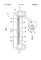
- FIG. 1is an end-section view of a packaged integrated circuit die having the present invention adhesion enhanced layer deposited thereon.
- FIG. 2is an enlarged partial view of FIG. 1,
- FIG. 1is an end-section view of packaged integrated circuit (IC) 10.
- Lead frame 15is disposed over IC die 20, the lead frame including inner and outer lead finger portions 25 and 30, respectively.
- Inner lead fingers 25are adjacent die pads 35, and outer lead fingers 30 extend outward of mold compound packaging 40 for connection with appropriate external circuitry.
- Insulator adhesive tape strips 45are disposed between inner lead fingers 25 and frontside 50 of die 20 to adhere the lead fingers to the die.
- Integrated circuitryis disposed on frontside 50 of die 20.
- Wire bonds 52communicate between inner lead fingers 25 and die pads 35 for making the electrical connection between the die and the lead fingers.
- Metal layer 55is shown deposited over backside 60 of die 20. Metal layer 55 enhances adhesion of die 20 with mold compound 40. Metal layer 55 is deposited over die 20 using an electroplating process or electroless coating process well known in the art prior to packaging of the die with mold compound 40.
- Metal layer 55provides a uniform wetting surface for mold compound 40 to adhere better to die 20. Although shown in its hardened and cured state, mold compound 40 is in a flowing state when it is initially heated over and molded around die 20. Consequently, the uniform wetting surface provided by layer 55 enhances the adhesion between the die and the mold compound.
- metal layer 55is substantially oxide free.
- the metal layeris either palladium (Pd) or copper (Cu), or a combination thereof, although it is obvious other metals may likewise suffice.
- copperis cheaper in cost, it retains more oxide which counteracts the intended adhesion. Palladium is more expensive, but provides a substantially oxide-free layer for effectuating a good bond with the mold compound.
- metal layer 55actually comprises a plurality of layers as shown in FIG. 2. Namely, a cheaper, thicker layer 65 of copper deposited over backside 60 of die 20 provides a good barrier to the oxide on die 20.
- a thinner layer 70 of palladiumis deposited over the copper layer to provide an even better uniform wetting surface.
- the palladiumis also substantially free from oxide.
- the present inventionreduces this potential package cracking problem. Consequently, no baking of the moisture out of the mold compound is needed, and no "dry packaging" the device for shipping purposes is needed.
Landscapes
- Physics & Mathematics (AREA)
- Condensed Matter Physics & Semiconductors (AREA)
- General Physics & Mathematics (AREA)
- Engineering & Computer Science (AREA)
- Computer Hardware Design (AREA)
- Microelectronics & Electronic Packaging (AREA)
- Power Engineering (AREA)
- Encapsulation Of And Coatings For Semiconductor Or Solid State Devices (AREA)
- Structures Or Materials For Encapsulating Or Coating Semiconductor Devices Or Solid State Devices (AREA)
Abstract
Description
This is a division of application Ser. No. 08/731,793, filed Oct. 18, 1996, now U.S. Pat. No. 5,760,468.
This invention relates in general to a semiconductor die packaging technique and, more particularly, to a die having a metal layer backside for enhanced adhesion of the die in a Leads On Chip (LOC) package system.
A semiconductor integrated circuit (IC) packaged device generally includes an IC chip (die) being connected to inner leads of a lead frame by wire bonds. The chip, wire bonds, and inner leads are completely encapsulated (packaged) for protection with a substance, such as plastic. Outer leads communicate with the inner leads of the lead frame, but the outer leads typically remain exposed for mounting of the packaged device to external circuitry, such as a printed circuit board. Conventionally, encapsulation occurs by a transfer molding technique wherein the encapsulation substance is a thermoset epoxy molded around and to the die and lead frame and subsequently cured.
In a conventional IC packaged device, a semiconductor die is placed on and bonded to a center die paddle of a lead frame for support. Inner lead fingers of the lead frame approach the paddle but do not contact or communicate with the paddle. Rather, wire bonds communicate between contact pads on the die and the inner lead fingers of the lead frame by spanning the gap between the die and the fingers. The wire bonds allow for the transmission of the electrical signals to and from the die and the lead frame.
However, to shrink the conventional packaging requirements, techniques such as the Lead On Chip (LOC) method have been developed. The LOC technique disposes the inner lead fingers of a lead frame directly over the die (or IC chip) rather than away from the die. Double-sided adhesive insulating tape attaches the conductive lead fingers to the die so that no gap exists between the die and lead fingers. Wire bonds communicate between the contact pads on the die and the inner lead fingers which are disposed over the insulating tape directly over a portion of the die adjacent the die pads.
This LOC technique allows the entire packaging of the IC device to be smaller because the inner lead fingers are disposed directly over the die rather than separate from the die. Similar to LOC, other variations of using an adhesive tape for adhering lead fingers and, consequently, shrinking packaging requirements include a Tape Under Frame technique and a Leads Under Die method.
Although IC packaging is minimized in each of these packaging techniques that uses an adhesive tape, other problems surface. One such problem in the LOC technique is the difficulty of obtaining a good, solid adhesive bond between the die and the package. One reason a solid bond is not achieved is because the oxide on the silicon die substrate does not lend itself to uniform wetting, which is necessary for good adhesion with the liquid mold compound.
When a die does not bond well with the mold compound package, delamination may occur and the device may potentially be ruined during the manufacturing process or surface mount of the package. Since production environment areas retain a substantial humidity level to reduce static buildup, i.e., often about 50%, moisture absorbs into the mold compound and can penetrate delaminated areas between the die and mold compound. When the moisture is converted to steam from heat processes and the steam pressure is greater than the strength of the adhesion couple between the mold compound and the die, the mold compound will crack or explode with a "popcorn" effect.
To overcome this potential package cracking problem, one technique has been to bake the moisture out of the mold compound to ensure a low moisture content within the package. Another step is to place the device in a "dry package" for shipping purposes by placing the final semiconductor chip product in a shipping container with a desiccant drying agent, such as silica gel. Although these techniques are commonly used in the semiconductor industry, they provide only a temporary solution. Namely, when a semiconductor manufacturer ships a "dried" packaged device by following these techniques, the device may still absorb moisture at a customer's site after the device is removed from the shipping container materials. Furthermore, if the die has delaminated even slightly, the package is subject to moisture penetration again and the package may subsequently crack if exposed to sufficient heat.
Another technique for reducing delamination potential is disclosed in U.S. Pat. No. 5,227,661 issued to Heinen on Jul. 13, 1993. Although this method provides a working solution, it retains disadvantages by its use of aminopropyltriethoxsilane as a coating on the die.
Obviously, the foregoing problems and solutions associated with providing a good bond between a die and a die package to avoid delamination and cracking of the package are undesirable aspects of conventional semiconductor packaging techniques. Accordingly, objects of the present invention are to provide an improved bonding between a semiconductor die and its encapsulating package in order to decrease delamination potential of the die from the package.
According to principles of the present invention in its preferred embodiment, a backside of a semiconductor die includes a metal layer deposited thereon for enhancing adhesion between the die and a mold compound package. The metal layer is substantially oxide free. The die is coated with a layer or layers of copper (Cu) and/or palladium (Pd) by electroplating or electroless coating techniques.
According to further principles of the present invention, the metal layer preferably comprises approximately 50 micro inches of a Cu layer deposited over the backside of the die and approximately 2 to 3 micro inches of a Pd layer deposited over the Cu layer.
Advantageously, the metal layer on the die provides a uniform wetting surface for better adhesion of the die with the mold compound during encapsulation. The increased adhesion reduces delamination potential of the die from the package and, consequently, reduces cracking of the package.
The aforementioned principles of the present invention provide an adhesion enhanced semiconductor die for improving adhesion of the die with a mold compound packaging. Other objects, advantages, and capabilities of the present invention will become more apparent as the description proceeds.
FIG. 1 is an end-section view of a packaged integrated circuit die having the present invention adhesion enhanced layer deposited thereon.
FIG. 2 is an enlarged partial view of FIG. 1,
FIG. 1 is an end-section view of packaged integrated circuit (IC) 10.Lead frame 15 is disposed over IC die 20, the lead frame including inner and outerlead finger portions Inner lead fingers 25 areadjacent die pads 35, andouter lead fingers 30 extend outward ofmold compound packaging 40 for connection with appropriate external circuitry.
Insulatoradhesive tape strips 45 are disposed betweeninner lead fingers 25 andfrontside 50 of die 20 to adhere the lead fingers to the die. Integrated circuitry is disposed onfrontside 50 of die 20.Wire bonds 52 communicate betweeninner lead fingers 25 and diepads 35 for making the electrical connection between the die and the lead fingers.
In its preferred embodiment,metal layer 55 is substantially oxide free. Also, preferably, the metal layer is either palladium (Pd) or copper (Cu), or a combination thereof, although it is obvious other metals may likewise suffice. Although copper is cheaper in cost, it retains more oxide which counteracts the intended adhesion. Palladium is more expensive, but provides a substantially oxide-free layer for effectuating a good bond with the mold compound. Although a single metal layer suffices to provide the advantages of the present invention, in its preferred embodiment,metal layer 55 actually comprises a plurality of layers as shown in FIG. 2. Namely, a cheaper,thicker layer 65 of copper deposited overbackside 60 ofdie 20 provides a good barrier to the oxide ondie 20. Athinner layer 70 of palladium is deposited over the copper layer to provide an even better uniform wetting surface. The palladium is also substantially free from oxide. Preferably, about 50 micro inches of copper and approximately 2 to 3 micro inches of palladium are deposited. Consequently, this combination of metal layers provides the enhancedadhesion layer 55 ondie 20 and, together, provide a good balance of cost and effectiveness.
As previously mentioned, when a die does not bond well with the mold compound package, delamination may occur and the device may potentially be ruined during the manufacturing process or surface mount of the package because of moisture penetration between the die and compound. When the moisture is converted to steam from heat processes and the steam pressure is greater than the strength of the adhesion couple between the mold compound and the die, the mold compound will crack or explode with a "popcorn" effect.
The present invention, as described and diagramed, reduces this potential package cracking problem. Consequently, no baking of the moisture out of the mold compound is needed, and no "dry packaging" the device for shipping purposes is needed.
What has been described above are the preferred embodiments for a semiconductor die having a metal layer backside for enhancing adhesion between the die and its mold compound packaging. It is clear that the present invention provides a powerful tool for reducing delamination potential of a die and subsequent cracking of the mold compound packaging. While the present invention has been described by reference to specific embodiments, it will be apparent that other alternative embodiments and methods of implementation or modification may be employed without departing from the true spirit and scope of the invention.
Claims (18)
1. A method of enhancing adhesion of a semiconductor die with a mold compound, comprising:
depositing a layer of at least one substantially oxide-free metal directly on at least a portion of a back side of a die; and
encapsulating at least a portion of the back side of the die bearing the at least one substantially oxide-free metal layer with a mold compound.
2. The method of claim 1, wherein said depositing includes electroplating.
3. The method of claim 1, wherein said depositing includes electroless coating.
4. The method of claim 1, wherein said depositing includes depositing a plurality of metals, at least the last deposited of which comprises a substantially oxide-free metal.
5. The method of claim 1, further including selecting said at least one substantially oxide-free metal from the group comprising palladium and copper.
6. The method of claim 1, wherein said depositing is effected over an entirety of the back side of the die.
7. The method of claim 6, wherein said encapsulating is effected over the surface bearing the at least one substantially oxide-free metal layer.
8. A method of enhancing adhesion of a semiconductor die with a mold compound, comprising:
depositing at least one substantially oxide-free metal in contact with at least a portion of a back side of a die; and
covering said at least a portion of the back side with a mold compound.
9. The method of claim 8, wherein said depositing comprises electroplating.
10. The method of claim 8, wherein said depositing comprises electroless coating.
11. The method of claim 8, wherein said depositing comprises depositing a plurality of metals, at least the last of which comprises a substantially oxide-free metal.
12. The method of claim 8, further including selecting said at least one substantially oxide-free metal from palladium and copper.
13. A method of enhancing adhesion of a semiconductor die with a mold compound, comprising:
depositing at least one substantially oxide-free metal in contact with a surface of a die; and
adhering a mold compound to said at least one substantially oxide-free metal.
14. The method of claim 13, wherein said depositing comprises electroplating.
15. The method of claim 13, wherein said depositing comprises electroless coating.
16. The method of claim 13, wherein said depositing comprises depositing a plurality of metals, at least the last of which comprises a substantially oxide-free metal.
17. The method of claim 13, further including selecting said at least one substantially oxide-free metal from palladium and copper.
18. The method of claim 13, wherein said adhering comprises covering at least a portion of the surface of the die with said mold compound.
Priority Applications (6)
| Application Number | Priority Date | Filing Date | Title |
|---|---|---|---|
| US08/963,395US6066514A (en) | 1996-10-18 | 1997-11-03 | Adhesion enhanced semiconductor die for mold compound packaging |
| US09/394,180US6316292B1 (en) | 1994-09-14 | 1999-09-10 | Adhesion enhanced semiconductor die for mold compound packaging |
| US09/873,581US6489186B2 (en) | 1994-09-14 | 2001-06-04 | Adhesion enhanced semiconductor die for mold compound packaging |
| US10/309,643US6740545B2 (en) | 1994-09-14 | 2002-12-03 | Adhesion enhanced semiconductor die for mold compound packaging |
| US10/852,632US20050001295A1 (en) | 1994-09-14 | 2004-05-24 | Adhesion enhanced semiconductor die for mold compound packaging |
| US11/188,157US20050253243A1 (en) | 1994-09-14 | 2005-07-22 | Semiconductor device structure with adhesion-enhanced semiconductor die |
Applications Claiming Priority (2)
| Application Number | Priority Date | Filing Date | Title |
|---|---|---|---|
| US08/731,793US5760468A (en) | 1994-09-14 | 1996-10-18 | Adhesion enhanced semiconductor die for mold compound packaging |
| US08/963,395US6066514A (en) | 1996-10-18 | 1997-11-03 | Adhesion enhanced semiconductor die for mold compound packaging |
Related Parent Applications (1)
| Application Number | Title | Priority Date | Filing Date |
|---|---|---|---|
| US08/731,793DivisionUS5760468A (en) | 1994-09-14 | 1996-10-18 | Adhesion enhanced semiconductor die for mold compound packaging |
Related Child Applications (1)
| Application Number | Title | Priority Date | Filing Date |
|---|---|---|---|
| US09/394,180ContinuationUS6316292B1 (en) | 1994-09-14 | 1999-09-10 | Adhesion enhanced semiconductor die for mold compound packaging |
Publications (1)
| Publication Number | Publication Date |
|---|---|
| US6066514Atrue US6066514A (en) | 2000-05-23 |
Family
ID=24940965
Family Applications (6)
| Application Number | Title | Priority Date | Filing Date |
|---|---|---|---|
| US08/963,395Expired - LifetimeUS6066514A (en) | 1994-09-14 | 1997-11-03 | Adhesion enhanced semiconductor die for mold compound packaging |
| US09/394,180Expired - Fee RelatedUS6316292B1 (en) | 1994-09-14 | 1999-09-10 | Adhesion enhanced semiconductor die for mold compound packaging |
| US09/873,581Expired - LifetimeUS6489186B2 (en) | 1994-09-14 | 2001-06-04 | Adhesion enhanced semiconductor die for mold compound packaging |
| US10/309,643Expired - Fee RelatedUS6740545B2 (en) | 1994-09-14 | 2002-12-03 | Adhesion enhanced semiconductor die for mold compound packaging |
| US10/852,632AbandonedUS20050001295A1 (en) | 1994-09-14 | 2004-05-24 | Adhesion enhanced semiconductor die for mold compound packaging |
| US11/188,157AbandonedUS20050253243A1 (en) | 1994-09-14 | 2005-07-22 | Semiconductor device structure with adhesion-enhanced semiconductor die |
Family Applications After (5)
| Application Number | Title | Priority Date | Filing Date |
|---|---|---|---|
| US09/394,180Expired - Fee RelatedUS6316292B1 (en) | 1994-09-14 | 1999-09-10 | Adhesion enhanced semiconductor die for mold compound packaging |
| US09/873,581Expired - LifetimeUS6489186B2 (en) | 1994-09-14 | 2001-06-04 | Adhesion enhanced semiconductor die for mold compound packaging |
| US10/309,643Expired - Fee RelatedUS6740545B2 (en) | 1994-09-14 | 2002-12-03 | Adhesion enhanced semiconductor die for mold compound packaging |
| US10/852,632AbandonedUS20050001295A1 (en) | 1994-09-14 | 2004-05-24 | Adhesion enhanced semiconductor die for mold compound packaging |
| US11/188,157AbandonedUS20050253243A1 (en) | 1994-09-14 | 2005-07-22 | Semiconductor device structure with adhesion-enhanced semiconductor die |
Country Status (1)
| Country | Link |
|---|---|
| US (6) | US6066514A (en) |
Cited By (33)
| Publication number | Priority date | Publication date | Assignee | Title |
|---|---|---|---|---|
| US6297546B1 (en)* | 1996-05-21 | 2001-10-02 | Micron Technology, Inc. | Underfill coating for LOC package |
| US6433418B1 (en)* | 1998-07-24 | 2002-08-13 | Fujitsu Limited | Apparatus for a vertically accumulable semiconductor device with external leads secured by a positioning mechanism |
| US20020175399A1 (en)* | 2000-08-24 | 2002-11-28 | James Stephen L. | Packaged microelectronic devices with pressure release elements and methods for manufacturing and using such packaged microelectronic devices |
| US6528354B1 (en)* | 2000-03-22 | 2003-03-04 | Seiko Instruments Inc. | Method of manufacturing a semiconductor device |
| US20030042581A1 (en)* | 2001-08-29 | 2003-03-06 | Fee Setho Sing | Packaged microelectronic devices and methods of forming same |
| US6558600B1 (en) | 2000-05-04 | 2003-05-06 | Micron Technology, Inc. | Method for packaging microelectronic substrates |
| US6564979B2 (en) | 2001-07-18 | 2003-05-20 | Micron Technology, Inc. | Method and apparatus for dispensing adhesive on microelectronic substrate supports |
| US20030104654A1 (en)* | 2000-06-28 | 2003-06-05 | Farnworth Warren M. | Recessed encapsulated microelectronic devices and methods for formation |
| US20030109083A1 (en)* | 2000-08-23 | 2003-06-12 | Ahmad Syed Sajid | Interconnecting substrates for electrical coupling of microelectronic components |
| US6622380B1 (en) | 2002-02-12 | 2003-09-23 | Micron Technology, Inc. | Methods for manufacturing microelectronic devices and methods for mounting microelectronic packages to circuit boards |
| US6653173B2 (en) | 2000-06-16 | 2003-11-25 | Micron Technology, Inc. | Method and apparatus for packaging a microelectronic die |
| US20040026773A1 (en)* | 2002-08-08 | 2004-02-12 | Koon Eng Meow | Packaged microelectronic components |
| US6693342B2 (en) | 2000-06-07 | 2004-02-17 | Micron Technology, Inc. | Thin microelectronic substrates and methods of manufacture |
| US20040031621A1 (en)* | 2002-08-19 | 2004-02-19 | Heng Puah Kia | Packaged microelectronic component assemblies |
| US20040100772A1 (en)* | 2002-11-22 | 2004-05-27 | Chye Lim Thiam | Packaged microelectronic component assemblies |
| US20040155331A1 (en)* | 2003-02-11 | 2004-08-12 | Blaine Thurgood | Packaged microelectronic devices and methods for packaging microelectronic devices |
| US6838760B1 (en) | 2000-08-28 | 2005-01-04 | Micron Technology, Inc. | Packaged microelectronic devices with interconnecting units |
| US20050001295A1 (en)* | 1994-09-14 | 2005-01-06 | King Jerrold L. | Adhesion enhanced semiconductor die for mold compound packaging |
| US20050093174A1 (en)* | 2003-10-31 | 2005-05-05 | Seng Eric T.S. | Reduced footprint packaged microelectronic components and methods for manufacturing such microelectronic components |
| US20050104228A1 (en)* | 2003-11-13 | 2005-05-19 | Rigg Sidney B. | Microelectronic devices, methods for forming vias in microelectronic devices, and methods for packaging microelectronic devices |
| US20050127478A1 (en)* | 2003-12-10 | 2005-06-16 | Hiatt William M. | Microelectronic devices and methods for filling vias in microelectronic devices |
| US20060035503A1 (en)* | 2003-08-29 | 2006-02-16 | Seng Eric T S | Invertible microfeature device packages and associated methods |
| US20060043534A1 (en)* | 2004-08-26 | 2006-03-02 | Kirby Kyle K | Microfeature dies with porous regions, and associated methods and systems |
| US20060261498A1 (en)* | 2005-05-17 | 2006-11-23 | Micron Technology, Inc. | Methods and apparatuses for encapsulating microelectronic devices |
| US20070045875A1 (en)* | 2005-08-30 | 2007-03-01 | Micron Technology, Inc. | Methods for wafer-level packaging of microfeature devices and microfeature devices formed using such methods |
| US20070132089A1 (en)* | 2005-12-13 | 2007-06-14 | Tongbi Jiang | Microelectronic devices and methods for manufacturing microelectronic devices |
| US20070181989A1 (en)* | 2006-02-08 | 2007-08-09 | Micron Technology, Inc. | Microelectronic devices, stacked microelectronic devices, and methods for manufacturing such devices |
| US20070210441A1 (en)* | 2006-03-08 | 2007-09-13 | Micron Technology, Inc. | Microelectronic device assemblies including assemblies with recurved leadframes, and associated methods |
| US20080012110A1 (en)* | 2006-07-17 | 2008-01-17 | Micron Technology, Inc. | Microelectronic packages with leadframes, including leadframes configured for stacked die packages, and associated systems and methods |
| US20080206930A1 (en)* | 2007-02-23 | 2008-08-28 | Micron Technology, Inc. | Systems and methods for compressing an encapsulant adjacent a semiconductor workpiece |
| US20080224291A1 (en)* | 2007-03-13 | 2008-09-18 | Micron Technology, Inc. | Packaged semiconductor components having substantially rigid support members and methods of packaging semiconductor components |
| US20090026600A1 (en)* | 2007-07-24 | 2009-01-29 | Micron Technology, Inc. | Microelectronic die packages with metal leads, including metal leads for stacked die packages, and associated systems and methods |
| US20090045489A1 (en)* | 2007-08-16 | 2009-02-19 | Micron Technology, Inc. | Microelectronic die packages with leadframes, including leadframe-based interposer for stacked die packages, and associated systems and methods |
Families Citing this family (7)
| Publication number | Priority date | Publication date | Assignee | Title |
|---|---|---|---|---|
| JP4014071B2 (en)* | 2000-03-13 | 2007-11-28 | 三菱電機株式会社 | AC generator, winding assembly thereof, and method of manufacturing winding assembly |
| JP4346333B2 (en)* | 2003-03-26 | 2009-10-21 | 新光電気工業株式会社 | Method for manufacturing multilayer circuit board incorporating semiconductor element |
| DE102005030946B4 (en)* | 2005-06-30 | 2007-09-27 | Infineon Technologies Ag | Semiconductor device with wiring substrate and solder balls as a connecting element and method for producing the semiconductor device |
| WO2008127807A1 (en)* | 2007-03-09 | 2008-10-23 | University Of Virginia Patent Foundation | Systems and methods of laser texturing of material surfaces and their applications |
| DE102007046275A1 (en)* | 2007-09-27 | 2009-04-16 | Siemens Ag | Electric drive system |
| US7943434B2 (en)* | 2008-03-21 | 2011-05-17 | Occam Portfolio Llc | Monolithic molded flexible electronic assemblies without solder and methods for their manufacture |
| JP6073637B2 (en)* | 2012-10-18 | 2017-02-01 | 株式会社小糸製作所 | Electronic unit |
Citations (15)
| Publication number | Priority date | Publication date | Assignee | Title |
|---|---|---|---|---|
| US3686539A (en)* | 1970-05-04 | 1972-08-22 | Rca Corp | Gallium arsenide semiconductor device with improved ohmic electrode |
| US3902148A (en)* | 1970-11-27 | 1975-08-26 | Signetics Corp | Semiconductor lead structure and assembly and method for fabricating same |
| US4024570A (en)* | 1974-09-17 | 1977-05-17 | Siemens Aktiengesellschaft | Simplified housing structure including a heat sink for a semiconductor unit |
| US4546374A (en)* | 1981-03-23 | 1985-10-08 | Motorola Inc. | Semiconductor device including plateless package |
| US4631805A (en)* | 1981-03-23 | 1986-12-30 | Motorola Inc. | Semiconductor device including plateless package fabrication method |
| JPH0499362A (en)* | 1990-08-18 | 1992-03-31 | Seiko Epson Corp | semiconductor equipment |
| JPH04162551A (en)* | 1990-10-24 | 1992-06-08 | Mitsubishi Electric Corp | Semiconductor integrated circuit device |
| US5227661A (en)* | 1990-09-24 | 1993-07-13 | Texas Instruments Incorporated | Integrated circuit device having an aminopropyltriethoxysilane coating |
| US5313102A (en)* | 1989-12-22 | 1994-05-17 | Texas Instruments Incorporated | Integrated circuit device having a polyimide moisture barrier coating |
| US5360991A (en)* | 1993-07-29 | 1994-11-01 | At&T Bell Laboratories | Integrated circuit devices with solderable lead frame |
| US5402006A (en)* | 1992-11-10 | 1995-03-28 | Texas Instruments Incorporated | Semiconductor device with enhanced adhesion between heat spreader and leads and plastic mold compound |
| US5449951A (en)* | 1992-01-17 | 1995-09-12 | Olin Corporation | Lead frames with improved adhesion to a polymer |
| US5576577A (en)* | 1993-05-24 | 1996-11-19 | Shinko Electric Industries Co., Ltd. | Multi-layer lead-frame for a semiconductor device |
| US5583372A (en)* | 1994-09-14 | 1996-12-10 | Micron Technology, Inc. | Adhesion enhanced semiconductor die for mold compound packaging |
| US5723369A (en)* | 1996-03-14 | 1998-03-03 | Lsi Logic Corporation | Method of flip chip assembly |
Family Cites Families (14)
| Publication number | Priority date | Publication date | Assignee | Title |
|---|---|---|---|---|
| US4026008A (en)* | 1972-10-02 | 1977-05-31 | Signetics Corporation | Semiconductor lead structure and assembly and method for fabricating same |
| US4348253A (en)* | 1981-11-12 | 1982-09-07 | Rca Corporation | Method for fabricating via holes in a semiconductor wafer |
| US4493856A (en)* | 1982-03-18 | 1985-01-15 | International Business Machines Corporation | Selective coating of metallurgical features of a dielectric substrate with diverse metals |
| US4702941A (en)* | 1984-03-27 | 1987-10-27 | Motorola Inc. | Gold metallization process |
| US4749120A (en)* | 1986-12-18 | 1988-06-07 | Matsushita Electric Industrial Co., Ltd. | Method of connecting a semiconductor device to a wiring board |
| US5236854A (en)* | 1989-12-11 | 1993-08-17 | Yukio Higaki | Compound semiconductor device and method for fabrication thereof |
| US5070297A (en)* | 1990-06-04 | 1991-12-03 | Texas Instruments Incorporated | Full wafer integrated circuit testing device |
| US5215801A (en)* | 1990-08-22 | 1993-06-01 | At&T Bell Laboratories | Silicone resin electronic device encapsulant |
| EP0502475B1 (en)* | 1991-03-04 | 1997-06-25 | Toda Kogyo Corporation | Method of plating a bonded magnet and a bonded magnet carrying a metal coating |
| US5302553A (en)* | 1991-10-04 | 1994-04-12 | Texas Instruments Incorporated | Method of forming a coated plastic package |
| US5317190A (en)* | 1991-10-25 | 1994-05-31 | International Business Machines Corporation | Oxygen assisted ohmic contact formation to N-type gallium arsenide |
| JP3572628B2 (en)* | 1992-06-03 | 2004-10-06 | セイコーエプソン株式会社 | Semiconductor device and manufacturing method thereof |
| US6262477B1 (en)* | 1993-03-19 | 2001-07-17 | Advanced Interconnect Technologies | Ball grid array electronic package |
| US6066514A (en)* | 1996-10-18 | 2000-05-23 | Micron Technology, Inc. | Adhesion enhanced semiconductor die for mold compound packaging |
- 1997
- 1997-11-03USUS08/963,395patent/US6066514A/ennot_activeExpired - Lifetime
- 1999
- 1999-09-10USUS09/394,180patent/US6316292B1/ennot_activeExpired - Fee Related
- 2001
- 2001-06-04USUS09/873,581patent/US6489186B2/ennot_activeExpired - Lifetime
- 2002
- 2002-12-03USUS10/309,643patent/US6740545B2/ennot_activeExpired - Fee Related
- 2004
- 2004-05-24USUS10/852,632patent/US20050001295A1/ennot_activeAbandoned
- 2005
- 2005-07-22USUS11/188,157patent/US20050253243A1/ennot_activeAbandoned
Patent Citations (15)
| Publication number | Priority date | Publication date | Assignee | Title |
|---|---|---|---|---|
| US3686539A (en)* | 1970-05-04 | 1972-08-22 | Rca Corp | Gallium arsenide semiconductor device with improved ohmic electrode |
| US3902148A (en)* | 1970-11-27 | 1975-08-26 | Signetics Corp | Semiconductor lead structure and assembly and method for fabricating same |
| US4024570A (en)* | 1974-09-17 | 1977-05-17 | Siemens Aktiengesellschaft | Simplified housing structure including a heat sink for a semiconductor unit |
| US4546374A (en)* | 1981-03-23 | 1985-10-08 | Motorola Inc. | Semiconductor device including plateless package |
| US4631805A (en)* | 1981-03-23 | 1986-12-30 | Motorola Inc. | Semiconductor device including plateless package fabrication method |
| US5313102A (en)* | 1989-12-22 | 1994-05-17 | Texas Instruments Incorporated | Integrated circuit device having a polyimide moisture barrier coating |
| JPH0499362A (en)* | 1990-08-18 | 1992-03-31 | Seiko Epson Corp | semiconductor equipment |
| US5227661A (en)* | 1990-09-24 | 1993-07-13 | Texas Instruments Incorporated | Integrated circuit device having an aminopropyltriethoxysilane coating |
| JPH04162551A (en)* | 1990-10-24 | 1992-06-08 | Mitsubishi Electric Corp | Semiconductor integrated circuit device |
| US5449951A (en)* | 1992-01-17 | 1995-09-12 | Olin Corporation | Lead frames with improved adhesion to a polymer |
| US5402006A (en)* | 1992-11-10 | 1995-03-28 | Texas Instruments Incorporated | Semiconductor device with enhanced adhesion between heat spreader and leads and plastic mold compound |
| US5576577A (en)* | 1993-05-24 | 1996-11-19 | Shinko Electric Industries Co., Ltd. | Multi-layer lead-frame for a semiconductor device |
| US5360991A (en)* | 1993-07-29 | 1994-11-01 | At&T Bell Laboratories | Integrated circuit devices with solderable lead frame |
| US5583372A (en)* | 1994-09-14 | 1996-12-10 | Micron Technology, Inc. | Adhesion enhanced semiconductor die for mold compound packaging |
| US5723369A (en)* | 1996-03-14 | 1998-03-03 | Lsi Logic Corporation | Method of flip chip assembly |
Cited By (113)
| Publication number | Priority date | Publication date | Assignee | Title |
|---|---|---|---|---|
| US20050001295A1 (en)* | 1994-09-14 | 2005-01-06 | King Jerrold L. | Adhesion enhanced semiconductor die for mold compound packaging |
| US20050253243A1 (en)* | 1994-09-14 | 2005-11-17 | King Jerrold L | Semiconductor device structure with adhesion-enhanced semiconductor die |
| US6297546B1 (en)* | 1996-05-21 | 2001-10-02 | Micron Technology, Inc. | Underfill coating for LOC package |
| US6433418B1 (en)* | 1998-07-24 | 2002-08-13 | Fujitsu Limited | Apparatus for a vertically accumulable semiconductor device with external leads secured by a positioning mechanism |
| US6528354B1 (en)* | 2000-03-22 | 2003-03-04 | Seiko Instruments Inc. | Method of manufacturing a semiconductor device |
| US6558600B1 (en) | 2000-05-04 | 2003-05-06 | Micron Technology, Inc. | Method for packaging microelectronic substrates |
| US20030209831A1 (en)* | 2000-05-04 | 2003-11-13 | Williams Vernon M. | Method and apparatus for packaging microelectronic substrates |
| US6693342B2 (en) | 2000-06-07 | 2004-02-17 | Micron Technology, Inc. | Thin microelectronic substrates and methods of manufacture |
| US6914317B2 (en) | 2000-06-07 | 2005-07-05 | Micron Technology, Inc. | Thin microelectronic substrates and methods of manufacture |
| US20040038500A1 (en)* | 2000-06-07 | 2004-02-26 | Larson Charles E. | Thin microelectronic substrates and methods of manufacture |
| US6677675B2 (en) | 2000-06-16 | 2004-01-13 | Micron Technology, Inc. | Microelectronic devices and microelectronic die packages |
| US6683388B2 (en) | 2000-06-16 | 2004-01-27 | Micron Technology, Inc. | Method and apparatus for packaging a microelectronic die |
| US6653173B2 (en) | 2000-06-16 | 2003-11-25 | Micron Technology, Inc. | Method and apparatus for packaging a microelectronic die |
| US6664139B2 (en) | 2000-06-16 | 2003-12-16 | Micron Technology, Inc. | Method and apparatus for packaging a microelectronic die |
| US6841423B2 (en) | 2000-06-28 | 2005-01-11 | Micron Technology, Inc. | Methods for formation of recessed encapsulated microelectronic devices |
| US6819003B2 (en) | 2000-06-28 | 2004-11-16 | Micron Technology Inc. | Recessed encapsulated microelectronic devices and methods for formation |
| US20030104654A1 (en)* | 2000-06-28 | 2003-06-05 | Farnworth Warren M. | Recessed encapsulated microelectronic devices and methods for formation |
| US20030106709A1 (en)* | 2000-08-23 | 2003-06-12 | Ahmad Syed Sajid | Interconnecting substrates for electrical coupling of microelectronic components |
| US6796028B2 (en) | 2000-08-23 | 2004-09-28 | Micron Technology, Inc. | Method of Interconnecting substrates for electrical coupling of microelectronic components |
| US6983551B2 (en) | 2000-08-23 | 2006-01-10 | Micron Technology, Inc. | Interconnecting substrates for electrical coupling of microelectronic components |
| US6982386B2 (en) | 2000-08-23 | 2006-01-03 | Micron Technology, Inc. | Interconnecting substrates for electrical coupling of microelectronic components |
| US20030109083A1 (en)* | 2000-08-23 | 2003-06-12 | Ahmad Syed Sajid | Interconnecting substrates for electrical coupling of microelectronic components |
| US20060180907A1 (en)* | 2000-08-24 | 2006-08-17 | Micron Technology, Inc. | Packaged microelectronic devices with pressure release elements and methods for manufacturing and using such packaged microelectonic devices |
| US6979595B1 (en) | 2000-08-24 | 2005-12-27 | Micron Technology, Inc. | Packaged microelectronic devices with pressure release elements and methods for manufacturing and using such packaged microelectronic devices |
| US7049685B2 (en) | 2000-08-24 | 2006-05-23 | Micron Technology, Inc. | Packaged microelectronic devices with pressure release elements and methods for manufacturing and using such packaged microelectronic devices |
| US20020175399A1 (en)* | 2000-08-24 | 2002-11-28 | James Stephen L. | Packaged microelectronic devices with pressure release elements and methods for manufacturing and using such packaged microelectronic devices |
| US7101737B2 (en) | 2000-08-28 | 2006-09-05 | Micron Technology, Inc. | Method of encapsulating interconnecting units in packaged microelectronic devices |
| US20050056919A1 (en)* | 2000-08-28 | 2005-03-17 | Cobbley Chad A. | Packaged microelectronic devices with interconnecting units and methods for manufacturing and using the interconnecting units |
| US6838760B1 (en) | 2000-08-28 | 2005-01-04 | Micron Technology, Inc. | Packaged microelectronic devices with interconnecting units |
| US7332376B2 (en) | 2000-08-28 | 2008-02-19 | Micron Technology, Inc. | Method of encapsulating packaged microelectronic devices with a barrier |
| US20070063335A1 (en)* | 2000-08-28 | 2007-03-22 | Micron Technology, Inc. | Packaged microelectronic devices with interconnecting units and methods for manufacturing and using the interconnecting units |
| US6564979B2 (en) | 2001-07-18 | 2003-05-20 | Micron Technology, Inc. | Method and apparatus for dispensing adhesive on microelectronic substrate supports |
| US20050023655A1 (en)* | 2001-08-29 | 2005-02-03 | Fee Setho Sing | Packaged microelectronic devices and methods of forming same |
| US6876066B2 (en) | 2001-08-29 | 2005-04-05 | Micron Technology, Inc. | Packaged microelectronic devices and methods of forming same |
| US20030042581A1 (en)* | 2001-08-29 | 2003-03-06 | Fee Setho Sing | Packaged microelectronic devices and methods of forming same |
| US6943450B2 (en) | 2001-08-29 | 2005-09-13 | Micron Technology, Inc. | Packaged microelectronic devices and methods of forming same |
| US7122905B2 (en) | 2002-02-12 | 2006-10-17 | Micron Technology, Inc. | Microelectronic devices and methods for mounting microelectronic packages to circuit boards |
| US6622380B1 (en) | 2002-02-12 | 2003-09-23 | Micron Technology, Inc. | Methods for manufacturing microelectronic devices and methods for mounting microelectronic packages to circuit boards |
| US7195957B2 (en) | 2002-08-08 | 2007-03-27 | Micron Technology, Inc. | Packaged microelectronic components |
| US20050026325A1 (en)* | 2002-08-08 | 2005-02-03 | Koon Eng Meow | Packaged microelectronic components |
| US6836009B2 (en) | 2002-08-08 | 2004-12-28 | Micron Technology, Inc. | Packaged microelectronic components |
| US9418872B2 (en) | 2002-08-08 | 2016-08-16 | Micron Technology, Inc. | Packaged microelectronic components |
| US8637973B2 (en) | 2002-08-08 | 2014-01-28 | Micron Technology, Inc. | Packaged microelectronic components with terminals exposed through encapsulant |
| US20080067642A1 (en)* | 2002-08-08 | 2008-03-20 | Micron Technology, Inc. | Packaged microelectronic components |
| US20040026773A1 (en)* | 2002-08-08 | 2004-02-12 | Koon Eng Meow | Packaged microelectronic components |
| US6933170B2 (en) | 2002-08-19 | 2005-08-23 | Micron Technology, Inc. | Packaged microelectronic component assemblies |
| US20040031621A1 (en)* | 2002-08-19 | 2004-02-19 | Heng Puah Kia | Packaged microelectronic component assemblies |
| US20040191964A1 (en)* | 2002-08-19 | 2004-09-30 | Heng Puah Kia | Packaged microelectronic component assemblies |
| US6781066B2 (en) | 2002-08-19 | 2004-08-24 | Micron Technology, Inc. | Packaged microelectronic component assemblies |
| US20040100772A1 (en)* | 2002-11-22 | 2004-05-27 | Chye Lim Thiam | Packaged microelectronic component assemblies |
| US6951982B2 (en) | 2002-11-22 | 2005-10-04 | Micron Technology, Inc. | Packaged microelectronic component assemblies |
| US6879050B2 (en) | 2003-02-11 | 2005-04-12 | Micron Technology, Inc. | Packaged microelectronic devices and methods for packaging microelectronic devices |
| US20040155331A1 (en)* | 2003-02-11 | 2004-08-12 | Blaine Thurgood | Packaged microelectronic devices and methods for packaging microelectronic devices |
| US7368810B2 (en) | 2003-08-29 | 2008-05-06 | Micron Technology, Inc. | Invertible microfeature device packages |
| US7259451B2 (en) | 2003-08-29 | 2007-08-21 | Micron Technology, Inc. | Invertible microfeature device packages |
| US20060035503A1 (en)* | 2003-08-29 | 2006-02-16 | Seng Eric T S | Invertible microfeature device packages and associated methods |
| US7691726B2 (en) | 2003-10-31 | 2010-04-06 | Micron Technology, Inc. | Reduced footprint packaged microelectronic components and methods for manufacturing such microelectronic components |
| US20050093174A1 (en)* | 2003-10-31 | 2005-05-05 | Seng Eric T.S. | Reduced footprint packaged microelectronic components and methods for manufacturing such microelectronic components |
| US7218001B2 (en) | 2003-10-31 | 2007-05-15 | Micron Technology, Inc. | Reduced footprint packaged microelectronic components and methods for manufacturing such microelectronic components |
| US20050104228A1 (en)* | 2003-11-13 | 2005-05-19 | Rigg Sidney B. | Microelectronic devices, methods for forming vias in microelectronic devices, and methods for packaging microelectronic devices |
| US7091124B2 (en) | 2003-11-13 | 2006-08-15 | Micron Technology, Inc. | Methods for forming vias in microelectronic devices, and methods for packaging microelectronic devices |
| US9653420B2 (en) | 2003-11-13 | 2017-05-16 | Micron Technology, Inc. | Microelectronic devices and methods for filling vias in microelectronic devices |
| US7413979B2 (en) | 2003-11-13 | 2008-08-19 | Micron Technology, Inc. | Methods for forming vias in microelectronic devices, and methods for packaging microelectronic devices |
| US7759800B2 (en) | 2003-11-13 | 2010-07-20 | Micron Technology, Inc. | Microelectronics devices, having vias, and packaged microelectronic devices having vias |
| US8084866B2 (en) | 2003-12-10 | 2011-12-27 | Micron Technology, Inc. | Microelectronic devices and methods for filling vias in microelectronic devices |
| US11177175B2 (en) | 2003-12-10 | 2021-11-16 | Micron Technology, Inc. | Microelectronic devices and methods for filling vias in microelectronic devices |
| US8748311B2 (en) | 2003-12-10 | 2014-06-10 | Micron Technology, Inc. | Microelectronic devices and methods for filing vias in microelectronic devices |
| US20050127478A1 (en)* | 2003-12-10 | 2005-06-16 | Hiatt William M. | Microelectronic devices and methods for filling vias in microelectronic devices |
| US20060043534A1 (en)* | 2004-08-26 | 2006-03-02 | Kirby Kyle K | Microfeature dies with porous regions, and associated methods and systems |
| US20070099397A1 (en)* | 2004-08-26 | 2007-05-03 | Micron Technology, Inc. | Microfeature dies with porous regions, and associated methods and systems |
| US20060261498A1 (en)* | 2005-05-17 | 2006-11-23 | Micron Technology, Inc. | Methods and apparatuses for encapsulating microelectronic devices |
| US20100327462A1 (en)* | 2005-08-30 | 2010-12-30 | Micron Technology, Inc. | Methods for wafer-level packaging of microfeature devices and microfeature devices formed using such methods |
| US7807505B2 (en) | 2005-08-30 | 2010-10-05 | Micron Technology, Inc. | Methods for wafer-level packaging of microfeature devices and microfeature devices formed using such methods |
| US20070045875A1 (en)* | 2005-08-30 | 2007-03-01 | Micron Technology, Inc. | Methods for wafer-level packaging of microfeature devices and microfeature devices formed using such methods |
| US8704380B2 (en) | 2005-08-30 | 2014-04-22 | Micron Technology, Inc. | Methods for wafer-level packaging of microfeature devices and microfeature devices formed using such methods |
| US20100062571A1 (en)* | 2005-12-13 | 2010-03-11 | Micron Technology, Inc. | Microelectronic devices and methods for manufacturing microelectronic devices |
| US7633157B2 (en) | 2005-12-13 | 2009-12-15 | Micron Technology, Inc. | Microelectronic devices having a curved surface and methods for manufacturing the same |
| US20070132089A1 (en)* | 2005-12-13 | 2007-06-14 | Tongbi Jiang | Microelectronic devices and methods for manufacturing microelectronic devices |
| US7888188B2 (en) | 2005-12-13 | 2011-02-15 | Micron Technology, Inc. | Method of fabicating a microelectronic die having a curved surface |
| US20070181989A1 (en)* | 2006-02-08 | 2007-08-09 | Micron Technology, Inc. | Microelectronic devices, stacked microelectronic devices, and methods for manufacturing such devices |
| US7671459B2 (en) | 2006-02-08 | 2010-03-02 | Micron Technologies, Inc. | Microelectronic devices, stacked microelectronic devices, and methods for manufacturing such devices |
| US10211114B2 (en) | 2006-02-28 | 2019-02-19 | Micron Technology, Inc. | Microelectronic devices, stacked microelectronic devices, and methods for manufacturing such devices |
| US9768121B2 (en) | 2006-02-28 | 2017-09-19 | Micron Technology, Inc. | Microelectronic devices, stacked microelectronic devices, and methods for manufacturing such devices |
| US9362141B2 (en) | 2006-02-28 | 2016-06-07 | Micron Technology, Inc. | Microelectronic devices, stacked microelectronic devices, and methods for manufacturing such devices |
| US8450839B2 (en) | 2006-02-28 | 2013-05-28 | Micron Technology, Inc. | Microelectronic devices, stacked microelectronic devices, and methods for manufacturing such devices |
| US20070210441A1 (en)* | 2006-03-08 | 2007-09-13 | Micron Technology, Inc. | Microelectronic device assemblies including assemblies with recurved leadframes, and associated methods |
| US7692931B2 (en) | 2006-07-17 | 2010-04-06 | Micron Technology, Inc. | Microelectronic packages with leadframes, including leadframes configured for stacked die packages, and associated systems and methods |
| US20100173454A1 (en)* | 2006-07-17 | 2010-07-08 | Micron Technology, Inc. | Microelectronic packages with leadframes, including leadframes configured for stacked die packages, and associated systems and methods |
| US8869387B2 (en) | 2006-07-17 | 2014-10-28 | Micron Technology, Inc. | Methods for making microelectronic die systems |
| US20080012110A1 (en)* | 2006-07-17 | 2008-01-17 | Micron Technology, Inc. | Microelectronic packages with leadframes, including leadframes configured for stacked die packages, and associated systems and methods |
| US7833456B2 (en) | 2007-02-23 | 2010-11-16 | Micron Technology, Inc. | Systems and methods for compressing an encapsulant adjacent a semiconductor workpiece |
| US20080206930A1 (en)* | 2007-02-23 | 2008-08-28 | Micron Technology, Inc. | Systems and methods for compressing an encapsulant adjacent a semiconductor workpiece |
| US20080224291A1 (en)* | 2007-03-13 | 2008-09-18 | Micron Technology, Inc. | Packaged semiconductor components having substantially rigid support members and methods of packaging semiconductor components |
| US9362208B2 (en) | 2007-03-13 | 2016-06-07 | Micron Technology, Inc. | Packaged semiconductor components having substantially rigid support members and methods of packaging semiconductor components |
| US7750449B2 (en) | 2007-03-13 | 2010-07-06 | Micron Technology, Inc. | Packaged semiconductor components having substantially rigid support members and methods of packaging semiconductor components |
| US10763185B2 (en) | 2007-03-13 | 2020-09-01 | Micron Technology, Inc. | Packaged semiconductor components having substantially rigid support members |
| US10312173B2 (en) | 2007-03-13 | 2019-06-04 | Micron Technology, Inc. | Packaged semiconductor components having substantially rigid support members and methods of packaging semiconductor components |
| US20100255636A1 (en)* | 2007-03-13 | 2010-10-07 | Micron Technology, Inc. | Packaged semiconductor components having substantially rigid support members and methods of packaging semiconductor components |
| US9960094B2 (en) | 2007-03-13 | 2018-05-01 | Micron Technology, Inc. | Packaged semiconductor components having substantially rigid support members and methods of packaging semiconductor components |
| US8906744B2 (en) | 2007-07-24 | 2014-12-09 | Micron Technology, Inc. | Microelectronic die packages with metal leads, including metal leads for stacked die packages, and associated systems and methods |
| US8536702B2 (en) | 2007-07-24 | 2013-09-17 | Micron Technology, Inc. | Microelectronic die packages with metal leads, including metal leads for stacked die packages, and associated systems and methods |
| US9165910B2 (en) | 2007-07-24 | 2015-10-20 | Micron Technology, Inc. | Microelectronic die packages with metal leads, including metal leads for stacked die packages, and associated systems and methods |
| US20110068454A1 (en)* | 2007-07-24 | 2011-03-24 | Micron Technology, Inc. | Microelectronic die packages with metal leads, including metal leads for stacked die packages, and associated systems and methods |
| US9653444B2 (en) | 2007-07-24 | 2017-05-16 | Micron Technology, Inc. | Microelectronic die packages with metal leads, including metal leads for stacked die packages, and associated systems and methods |
| US8198720B2 (en) | 2007-07-24 | 2012-06-12 | Micron Technology, Inc. | Microelectronic die packages with metal leads, including metal leads for stacked die packages, and associated systems and methods |
| US7843050B2 (en) | 2007-07-24 | 2010-11-30 | Micron Technology, Inc. | Microelectronic die packages with metal leads, including metal leads for stacked die packages, and associated systems and methods |
| US10396059B2 (en) | 2007-07-24 | 2019-08-27 | Micron Technology, Inc. | Microelectronic die packages with metal leads, including metal leads for stacked die packages, and associated systems and methods |
| US10056359B2 (en) | 2007-07-24 | 2018-08-21 | Micron Technology, Inc. | Microelectronic die packages with metal leads, including metal leads for stacked die packages, and associated systems and methods |
| US20090026600A1 (en)* | 2007-07-24 | 2009-01-29 | Micron Technology, Inc. | Microelectronic die packages with metal leads, including metal leads for stacked die packages, and associated systems and methods |
| US20110215453A1 (en)* | 2007-08-16 | 2011-09-08 | Micron Technology, Inc. | Microelectronic die packages with leadframes, including leadframe-based interposer for stacked die packages, and associated systems and methods |
| US7947529B2 (en) | 2007-08-16 | 2011-05-24 | Micron Technology, Inc. | Microelectronic die packages with leadframes, including leadframe-based interposer for stacked die packages, and associated systems and methods |
| US20090045489A1 (en)* | 2007-08-16 | 2009-02-19 | Micron Technology, Inc. | Microelectronic die packages with leadframes, including leadframe-based interposer for stacked die packages, and associated systems and methods |
| US8525320B2 (en) | 2007-08-16 | 2013-09-03 | Micron Technology, Inc. | Microelectronic die packages with leadframes, including leadframe-based interposer for stacked die packages, and associated systems and methods |
Also Published As
| Publication number | Publication date |
|---|---|
| US6489186B2 (en) | 2002-12-03 |
| US20010024840A1 (en) | 2001-09-27 |
| US20050253243A1 (en) | 2005-11-17 |
| US20050001295A1 (en) | 2005-01-06 |
| US20030082849A1 (en) | 2003-05-01 |
| US6740545B2 (en) | 2004-05-25 |
| US6316292B1 (en) | 2001-11-13 |
Similar Documents
| Publication | Publication Date | Title |
|---|---|---|
| US6066514A (en) | Adhesion enhanced semiconductor die for mold compound packaging | |
| US5583372A (en) | Adhesion enhanced semiconductor die for mold compound packaging | |
| US5581119A (en) | IC having heat spreader attached by glob-topping | |
| KR100445072B1 (en) | Bumped chip carrier package using lead frame and method for manufacturing the same | |
| US6482675B2 (en) | Substrate strip for use in packaging semiconductor chips and method for making the substrate strip | |
| US5434106A (en) | Integrated circuit device and method to prevent cracking during surface mount | |
| US5567656A (en) | Process for packaging semiconductor device | |
| US5951813A (en) | Top of die chip-on-board encapsulation | |
| JP2000269166A (en) | Method of manufacturing integrated circuit chip and semiconductor device | |
| US7226813B2 (en) | Semiconductor package | |
| JP2501953B2 (en) | Semiconductor device | |
| US6650005B2 (en) | Micro BGA package | |
| US5933708A (en) | Lead-on-chip semiconductor package and method for making the same | |
| WO1999049512A1 (en) | Semiconductor device and method of manufacturing the same | |
| JPS6077446A (en) | Sealed semiconductor device | |
| US6211563B1 (en) | Semiconductor package with an improved leadframe | |
| JP3642545B2 (en) | Resin-sealed semiconductor device | |
| JP3179845B2 (en) | Semiconductor device | |
| US6037652A (en) | Lead frame with each lead having a peel generation preventing means and a semiconductor device using same | |
| JP3060100U (en) | Suspended chip package | |
| GB2295722A (en) | Packaging integrated circuits | |
| JPH07263470A (en) | Mounting method of semiconductor chip | |
| JPH04252041A (en) | Manufacture of hybrid integrated circuit | |
| JPH01309357A (en) | Semiconductor device | |
| JPH09283689A (en) | Composite lead frame and manufacturing method thereof, and semiconductor device and manufacturing method thereof |
Legal Events
| Date | Code | Title | Description |
|---|---|---|---|
| STCF | Information on status: patent grant | Free format text:PATENTED CASE | |
| FEPP | Fee payment procedure | Free format text:PAYOR NUMBER ASSIGNED (ORIGINAL EVENT CODE: ASPN); ENTITY STATUS OF PATENT OWNER: LARGE ENTITY | |
| FPAY | Fee payment | Year of fee payment:4 | |
| CC | Certificate of correction | ||
| FPAY | Fee payment | Year of fee payment:8 | |
| FPAY | Fee payment | Year of fee payment:12 |