US6066265A - Micromachined silicon probe for scanning probe microscopy - Google Patents
Micromachined silicon probe for scanning probe microscopyDownload PDFInfo
- Publication number
- US6066265A US6066265AUS08/665,369US66536996AUS6066265AUS 6066265 AUS6066265 AUS 6066265AUS 66536996 AUS66536996 AUS 66536996AUS 6066265 AUS6066265 AUS 6066265A
- Authority
- US
- United States
- Prior art keywords
- layer
- tip
- cantilever
- etching
- silicon
- Prior art date
- Legal status (The legal status is an assumption and is not a legal conclusion. Google has not performed a legal analysis and makes no representation as to the accuracy of the status listed.)
- Expired - Lifetime
Links
- XUIMIQQOPSSXEZ-UHFFFAOYSA-NSiliconChemical compound[Si]XUIMIQQOPSSXEZ-UHFFFAOYSA-N0.000titleclaimsabstractdescription57
- 229910052710siliconInorganic materials0.000titleclaimsabstractdescription57
- 239000010703siliconSubstances0.000titleclaimsabstractdescription57
- 239000000523sampleSubstances0.000titleclaimsdescription154
- 238000004621scanning probe microscopyMethods0.000titledescription41
- 238000005530etchingMethods0.000claimsabstractdescription53
- 239000000463materialSubstances0.000claimsabstractdescription24
- 230000000873masking effectEffects0.000claimsabstractdescription17
- 239000000758substrateSubstances0.000claimsabstractdescription5
- 238000000034methodMethods0.000claimsdescription131
- 230000008569processEffects0.000claimsdescription47
- VYPSYNLAJGMNEJ-UHFFFAOYSA-NSilicium dioxideChemical compoundO=[Si]=OVYPSYNLAJGMNEJ-UHFFFAOYSA-N0.000claimsdescription38
- 238000004519manufacturing processMethods0.000claimsdescription31
- 239000000377silicon dioxideSubstances0.000claimsdescription19
- 230000008859changeEffects0.000claimsdescription18
- 238000003384imaging methodMethods0.000claimsdescription18
- 238000001020plasma etchingMethods0.000claimsdescription15
- 235000012239silicon dioxideNutrition0.000claimsdescription15
- 229910015844BCl3Inorganic materials0.000claimsdescription12
- 229910052581Si3N4Inorganic materials0.000claimsdescription12
- 239000007789gasSubstances0.000claimsdescription12
- HQVNEWCFYHHQES-UHFFFAOYSA-Nsilicon nitrideChemical compoundN12[Si]34N5[Si]62N3[Si]51N64HQVNEWCFYHHQES-UHFFFAOYSA-N0.000claimsdescription12
- FAQYAMRNWDIXMY-UHFFFAOYSA-NtrichloroboraneChemical compoundClB(Cl)ClFAQYAMRNWDIXMY-UHFFFAOYSA-N0.000claimsdescription12
- XPDWGBQVDMORPB-UHFFFAOYSA-NFluoroformChemical compoundFC(F)FXPDWGBQVDMORPB-UHFFFAOYSA-N0.000claimsdescription7
- 230000015572biosynthetic processEffects0.000claimsdescription7
- 229910021421monocrystalline siliconInorganic materials0.000claimsdescription7
- 238000012545processingMethods0.000claimsdescription6
- 239000011248coating agentSubstances0.000claimsdescription4
- 238000000576coating methodMethods0.000claimsdescription4
- 230000001590oxidative effectEffects0.000claimsdescription4
- 238000003486chemical etchingMethods0.000claimsdescription2
- 238000000059patterningMethods0.000claims5
- 239000002131composite materialSubstances0.000claims4
- 239000011810insulating materialSubstances0.000abstractdescription2
- 239000010410layerSubstances0.000description117
- 235000012431wafersNutrition0.000description58
- KWYUFKZDYYNOTN-UHFFFAOYSA-MPotassium hydroxideChemical compound[OH-].[K+]KWYUFKZDYYNOTN-UHFFFAOYSA-M0.000description42
- 238000004630atomic force microscopyMethods0.000description32
- 238000000429assemblyMethods0.000description11
- 230000000712assemblyEffects0.000description11
- 238000007796conventional methodMethods0.000description9
- 238000005259measurementMethods0.000description9
- KRHYYFGTRYWZRS-UHFFFAOYSA-NFluoraneChemical compoundFKRHYYFGTRYWZRS-UHFFFAOYSA-N0.000description8
- 230000003993interactionEffects0.000description8
- 230000003647oxidationEffects0.000description8
- 238000007254oxidation reactionMethods0.000description8
- 238000003631wet chemical etchingMethods0.000description8
- 229910007277Si3 N4Inorganic materials0.000description7
- 230000008901benefitEffects0.000description7
- 238000002465magnetic force microscopyMethods0.000description7
- 229910052751metalInorganic materials0.000description7
- 239000002184metalSubstances0.000description7
- 239000000126substanceSubstances0.000description7
- 239000012212insulatorSubstances0.000description6
- 238000001459lithographyMethods0.000description6
- 238000004574scanning tunneling microscopyMethods0.000description6
- ZOXJGFHDIHLPTG-UHFFFAOYSA-NBoronChemical compound[B]ZOXJGFHDIHLPTG-UHFFFAOYSA-N0.000description5
- 229910052796boronInorganic materials0.000description5
- 239000013078crystalSubstances0.000description5
- 230000003287optical effectEffects0.000description5
- 239000000243solutionSubstances0.000description5
- 238000013459approachMethods0.000description4
- 230000000694effectsEffects0.000description4
- 238000002513implantationMethods0.000description4
- 238000000542scanning thermal microscopyMethods0.000description4
- 238000012876topographyMethods0.000description4
- 230000005641tunnelingEffects0.000description4
- 238000005411Van der Waals forceMethods0.000description3
- 238000005229chemical vapour depositionMethods0.000description3
- 238000001514detection methodMethods0.000description3
- 239000007943implantSubstances0.000description3
- 150000002500ionsChemical class0.000description3
- 230000035945sensitivityEffects0.000description3
- 239000002356single layerSubstances0.000description3
- 238000001712DNA sequencingMethods0.000description2
- 229910052681coesiteInorganic materials0.000description2
- 230000001010compromised effectEffects0.000description2
- 229910052906cristobaliteInorganic materials0.000description2
- 238000011161developmentMethods0.000description2
- 238000002474experimental methodMethods0.000description2
- 229920002120photoresistant polymerPolymers0.000description2
- 230000002829reductive effectEffects0.000description2
- 238000005070samplingMethods0.000description2
- 230000003068static effectEffects0.000description2
- 229910052682stishoviteInorganic materials0.000description2
- 238000012546transferMethods0.000description2
- 229910052905tridymiteInorganic materials0.000description2
- 230000005534acoustic noiseEffects0.000description1
- 230000009471actionEffects0.000description1
- 230000001154acute effectEffects0.000description1
- 230000002411adverseEffects0.000description1
- 238000013019agitationMethods0.000description1
- 229910052782aluminiumInorganic materials0.000description1
- XAGFODPZIPBFFR-UHFFFAOYSA-NaluminiumChemical compound[Al]XAGFODPZIPBFFR-UHFFFAOYSA-N0.000description1
- 239000007864aqueous solutionSubstances0.000description1
- QVGXLLKOCUKJST-UHFFFAOYSA-Natomic oxygenChemical compound[O]QVGXLLKOCUKJST-UHFFFAOYSA-N0.000description1
- 230000000903blocking effectEffects0.000description1
- 230000005492condensed matter physicsEffects0.000description1
- 239000004020conductorSubstances0.000description1
- 238000011109contaminationMethods0.000description1
- 230000007812deficiencyEffects0.000description1
- 230000001419dependent effectEffects0.000description1
- 238000006073displacement reactionMethods0.000description1
- 238000001312dry etchingMethods0.000description1
- 238000010894electron beam technologyMethods0.000description1
- 238000000407epitaxyMethods0.000description1
- 230000005284excitationEffects0.000description1
- 239000012467final productSubstances0.000description1
- 239000011888foilSubstances0.000description1
- PCHJSUWPFVWCPO-UHFFFAOYSA-NgoldChemical compound[Au]PCHJSUWPFVWCPO-UHFFFAOYSA-N0.000description1
- 239000010931goldSubstances0.000description1
- 229910052737goldInorganic materials0.000description1
- 230000006872improvementEffects0.000description1
- 238000010978in-process monitoringMethods0.000description1
- 238000007689inspectionMethods0.000description1
- 230000000670limiting effectEffects0.000description1
- 239000007788liquidSubstances0.000description1
- 238000007567mass-production techniqueMethods0.000description1
- 238000004377microelectronicMethods0.000description1
- 238000002156mixingMethods0.000description1
- 238000012986modificationMethods0.000description1
- 230000004048modificationEffects0.000description1
- 238000012544monitoring processMethods0.000description1
- 229910052754neonInorganic materials0.000description1
- GKAOGPIIYCISHV-UHFFFAOYSA-Nneon atomChemical compound[Ne]GKAOGPIIYCISHV-UHFFFAOYSA-N0.000description1
- 239000001301oxygenSubstances0.000description1
- 229910052760oxygenInorganic materials0.000description1
- 238000002360preparation methodMethods0.000description1
- 238000004886process controlMethods0.000description1
- 238000001314profilometryMethods0.000description1
- 238000002310reflectometryMethods0.000description1
- 238000011160researchMethods0.000description1
- 238000000926separation methodMethods0.000description1
- HBMJWWWQQXIZIP-UHFFFAOYSA-Nsilicon carbideChemical compound[Si+]#[C-]HBMJWWWQQXIZIP-UHFFFAOYSA-N0.000description1
- 229910010271silicon carbideInorganic materials0.000description1
- 238000000992sputter etchingMethods0.000description1
- 238000003860storageMethods0.000description1
- 238000012360testing methodMethods0.000description1
- 238000011179visual inspectionMethods0.000description1
Images


Classifications
- G—PHYSICS
- G01—MEASURING; TESTING
- G01Q—SCANNING-PROBE TECHNIQUES OR APPARATUS; APPLICATIONS OF SCANNING-PROBE TECHNIQUES, e.g. SCANNING PROBE MICROSCOPY [SPM]
- G01Q60/00—Particular types of SPM [Scanning Probe Microscopy] or microscopes; Essential components thereof
- G01Q60/24—AFM [Atomic Force Microscopy] or apparatus therefor, e.g. AFM probes
- G01Q60/38—Probes, their manufacture, or their related instrumentation, e.g. holders
- B—PERFORMING OPERATIONS; TRANSPORTING
- B82—NANOTECHNOLOGY
- B82Y—SPECIFIC USES OR APPLICATIONS OF NANOSTRUCTURES; MEASUREMENT OR ANALYSIS OF NANOSTRUCTURES; MANUFACTURE OR TREATMENT OF NANOSTRUCTURES
- B82Y35/00—Methods or apparatus for measurement or analysis of nanostructures
Definitions
- the field of the inventionrelates generally to a probe for imaging or for effecting change in state at the atomic and near atomic level.
- the field of the inventionrelates to a monolithic probe for scanning probe microscopy applications, such as atomic force microscopy, as well as field emission tips, or the like, for effecting a change in state at the atomic level, and to a method for making such a probe in a reproducible, high volume manner.
- SPMScanning Probe Microscopy
- AFMatomic force microscopy
- MFMmagnetic force microscopy
- STMscanning tunneling microscopy
- SThMscanning thermal microscopy
- a related aspect of SPMalso uses a nanometer size tip such as an AFM or like tip to emit electrons for effecting a switching phenomenon, such as a change of state, change of phase, or localized change in resistivity or optical property at or near the surface of a material at the atomic scale.
- a probetypically comprises a mounting block, cantilever, and a tip assembly depending from the cantilever.
- the tip assemblyfurther comprises a high aspect ratio column and a tip having substantially atomic sharpness disposed on the distal end of the column.
- the tip of the tip assemblyfollows the surface to be imaged, and in most instances, moves up or down due to the tip interacting in some manner with atoms on the surface being imaged.
- the deflection of the cantileveris used to measure the interaction between the tip and the sample being scanned.
- the deflection of the tipis translated by techniques which are well known into an image of the surface.
- Other SPM applicationsutilize changes in resonant frequency or electrical current to measure interaction between the tip and the sample.
- AFMmeasures variations in the repulsive forces between the atoms on the surface to be imaged and the point of the tip of a tip assembly, which point is less than about 30 nanometers in diameter (i.e. it is "atomically sharp", meaning it is able to resolve images at an atomic level).
- the principle of atomic force microscopy (AFM) operationcan be applied to measure a variety of forces and image those forces, including ionic repulsion, van der Waals forces, capillary, electrostatic, magnetic and frictional forces.
- a major impact of AFMcan be expected to be made in many different research fields such as biology, electronics, and condensed matter physics. For example, magnetic force microscopy, an AFM technique, has now become an established experimental technique for the study of surface magnetic properties.
- AFMuses a tip assembly in a non-contact mode for imaging a sample surface.
- the tipIn the non-contact mode, the tip is maintained at a distance of approximately 50-150 ⁇ above the surface. This is necessary in situations in which tip contact may alter the sample surface.
- the interaction force between the tip and the sample surface being imagedcauses a measurable change in the cantilever status, such as deflection or shift in resonant frequency.
- Several techniqueshave been developed to detect the interaction force between the tip and sample.
- the most straightforward techniquedetects the force by measuring the static deflection of the cantilever, such as by an optical interferometer or by an integrated strain gauge such as a piezoresister (see for example Minne et. al., APL 67, Dec. 25, 1995).
- an optical interferometeror by an integrated strain gauge such as a piezoresister
- Significantly greater sensitivity to extremely small forcessuch as van der Waals forces, or the like, can be obtained by exciting the cantilever to mechanical resonance and measuring changes in the resonant frequency.
- a change in the resonant frequency of the cantileveroccurs due to atomic force interactions between the tip and the sample as the tip approaches the sample.
- a change in the resonant frequency of the cantileveris detected by keeping the excitation frequency constant and measuring a change in the vibration amplitude of the cantilever using a sensitive laser heterodyne probe.
- the resonant frequency of the cantileveris one critical parameter that must be carefully controlled in order to consistently image surfaces.
- An atomic force microscopealso can be used as a probe for tracking ultra high speed pulses in microelectronic devices.
- the AFM tipstays about 2 ⁇ above the sample surface. The tip is kept at that position by a gentle downward pressure exerted by the cantilever and a quantum mechanical repulsive force that prevents the tip from coming closer to the target surface.
- a stream of voltage pulsesare applied to the tip and to the device under test. The stream of pulses to the tip enable the AFM to be used as an extremely fast mixer or sampler. Sampling is necessary because the cantilever cannot vibrate fast enough to keep up with the voltage pulses. This enables a researcher to take stroboscopic like images of waveforms.
- Very short pulses to the AFM tipcan freeze the action of a high speed waveform.
- the application of signal mixingutilizes pulses up to 20 GHz and sampling with 100 picosecond time resolution. This enables a researcher to create logic maps of ultra high speed nano scale circuits by scanning their topographies and voltage characteristics at the same time.
- a magnetic tipIn the magnetic force microscope (MFM), a magnetic tip is mounted on a flexible cantilever and is used to image magnetic field patterns.
- the magnetic dipole of the tipinteracts with the stray magnetic fields from a sample surface. Stray magnetic fields exert a force on the magnetized tip.
- the gradient of stray magnetic fieldsalters the resonant frequency of the cantilever. The change in resonant frequency is used to provide information regarding the sample surface.
- the shape and magnetic properties of the tip used in MFMare critical to obtaining a quantative measure of the sample surface of magnetic properties. See for example Proksch et al., APL 66, May 8, 1995, p. 2582.
- the tipis held at a constant tunneling current by maintaining a constant vertical height from the image to be scanned.
- a constant vertical heightis maintained by moving the tip assembly up or down on the Z-axis. Movement of the tip is therefore achieved by external control and not by a force directly acting between the tip and the surface.
- a scanning thermal (SThM) probecan be used to profile atomic features on both insulating and conducting crystals, or the like.
- the scanning thermal probecomprises a thermal sensor, such a thermocouple, disposed at the apex of a probe tip.
- a thermal sensorsuch as thermocouple
- the thermocoupleheats up to an equilibrium temperature above the ambient value. If the tip now approaches a sample surface (an insulator, conductor or even a liquid) it cools down due to heat transfer from the tip to the sample.
- the tip temperature which is detected by the thermocouplethen can used to control tip-spacing in much the same way as a tunneling current is used in a STM as the tip is scanned across the surface.
- thermoelectric voltageWhen the tip is vibrated by a few tens of angstroms ( ⁇ ) in the vertical direction, the ac change in the thermoelectric voltage is used as a monitor of the tip-sample spacing. This renders the system immune to ambient temperature variations caused by room temperature fluctuations and air currents in the vicinity of the probe tip.
- a SThM probecan also be used to measure surface feature temperatures or thermal conductivities with high spatial resolution. See for example Lai et al., "Thermal Detection of Device Failure by Atomic Force Microscopy," IEEE Electron Device Lett., 16 (1995), pp. 312-315.
- the scanning probeis thermally activated and sensed to obtain both a topographic and thermal image of the surface.
- Another application relating to SPMuses a probe tip having a nanometer size apex to emit electrons from the apex to the sample surface.
- the electron emissionis used to effect a switching phenomenon in the sample surface at the atomic scale.
- the switching phenomenonis typically a change of state, change of phase, localized change in resistivity or optical property, or the like.
- SPM applicationuses the electrical interaction between AFM tip and sample surface to produce a localized enhanced oxidation of the sample (Dagata, Science 270, Dec. 8, 1995). This technique can be used to fabricate electronic devices with dimensions of 10 nm or less.
- the foregoing SPM methodsmandate a number of requirements that probes must exhibit to successfully implement SPM.
- the tip assembliesmust have the following associated characteristics.
- the mounting blockmust be characterized by a geometry which is suited to the particular use of the probe.
- the mounting blockmust fit into the SPM, or like instrument, as well as be of sufficient size such that it can be manipulated by the operator of the instrument. This is critical since only the mounting block is large enough to be physically manipulated by the operator of the instrument.
- the mounting blockmust be characterized by sufficient rigidity to provide a stable and rigid support for the cantilever. The relationship of the cantilever to the mounting block must be consistent. That is, the cantilever must always be in the same place on the mounting block and extend outwardly for a predetermined distance for each probe made for a specific application.
- the mounting blockmust be supported by a larger structure, such as a silicon wafer, from which it is processed in such a way that the mounting block can undergo necessary processing and yet easily be released from the wafer without damage upon completion of processing. Further, the mounting block must be of sufficient dimensions to allow ready attachment to the SPM device by an operator.
- the cantilevermust have suitable dimensions and mechanical properties to control the cantilever spring constant and resonant frequency. Once the desired tip geometry is determined, the dimensions and material from which the cantilever are made determine the resonant frequency, spring constant, and Q value of the cantilever. Detection of the shift in resonant frequency of the cantilever is a powerful method for measuring narrow spacings and thus imaging a sample surface. The most sensitive force microscopes use resonance enhancement of a vibrating cantilever to detect forces as small as 3 ⁇ 10 -13 N. With resonance enhancement, either a shift in the resonant frequency or a decrease in the vibration amplitude can be used for proximity detection. Monitoring the vibration amplitude is equivalent to measuring the Q of the vibrating lever as it interacts with the surface.
- the cantilevers in scanning force microscopy applicationsneed a small spring constant to achieve high sensitivity, but also require a high resonant frequency to achieve reasonable scanning speed, and to render the cantilever insensitive to acoustic noise and external vibrations.
- the limited ability of conventional SPM probes to operate at high scanning speedsis a well known problem (Manalis et al., APL 68, Feb. 5, 1996).
- the cantileverIn order to achieve low spring constant and high resonant frequency simultaneously, the cantilever must have low mass, as shown by the following relationship of resonant frequency ⁇ with spring constant k and cantilever mass m: ##EQU1## A low mass can be achieved by making the cantilevers physically small.
- Typical cantileversare 100-400 microns ( ⁇ m) in length, 10-50 ⁇ m in width, and have a thickness in a range of from 0.1-10 ⁇ m. Thus, the size of the cantilever and the tip must be carefully controlled to assure that the cantilever has the correct resonant frequency, spring constant, and Q value for use in a particular SPM method.
- the cantilevermust further have dimensions appropriate to the measurement being performed. For example, if a laser interferometer is used to measure cantilever displacement, the cantilever must be of sufficient width such that the reflected laser light can be accurately determined.
- the tip assemblymust be suited to the particular use. Image formation at the subnanometer level is not a linear process, and the size and shape of the tip are critical. Accurate measurement of a sample surface is not possible unless the dimensions of the probe are known and are consistent from one tip assembly to the next. If the size and shape of a probe are not accurately known and the size and shape vary from probe to probe, distortions in measurement may be induced. Such distortions must then be removed by complex compensation circuitry or software.
- the tip assemblymust comprise a high aspect ratio column depending from the cantilever.
- the distal end of the columnculminates in a tip which is preferably characterized by a high cone angle.
- the column and tipmust be characterized by high torsional rigidity.
- the columnpreferably tapers to a minimal diameter tip. This advantageously enables the tip to enter high topology surfaces for accurate imaging.
- the tipshould be characterized by a high cone angle and a diameter of less than 30 nanometers.
- the size of the tipmust be similar to or smaller than that of the object to be studied. To achieve atomic resolution, the tip must end with a small cluster of atoms. To scan a micron deep hole, the tip must not exceed the diameter of the hole for a full micron back from the apex. In addition, an extremely narrow tip with a high cone angle may be necessary to measure samples with steep or reentrant topography. This must be achieved without comprising the stiffness or stability of the tip. Reproducibly making such high aspect ratio probes is one of the most difficult tasks in conventional scanning force microscopy.
- a point 102 of a probe 100may be too blunt or have a diameter too large to reach the bottom of a trench in an object 106 to be scanned.
- the true depth of the trenchcannot be extracted from the scan 104.
- a serious problem in conventional scanning force microscopyarises when a surface to be imaged has regions with steep slopes. On lithographically patterned surfaces, the problem is especially acute. Deep, narrow trenches and holes with undercut sidewalls are common. The ability of a scanning force microscope probe to accurately image surface topography depends strongly on the size and shape of the probe.
- FIG. 1Bshows the desirability of a high cone angle for a scanning force microscope probe.
- the angle ⁇is greater than ⁇ so that the tip with such a high cone angle ⁇ faithfully follows the left side of the trench.
- Such a probeis limited only in its ability to image the slope of the right side of the trench.
- FIG. 1Calso shows a probe with a high cone angle as in FIG. 1B but having a tip point with a large radius of curvature.
- the scan line 104 produced by a blunt probe 102 encountering a sudden stepcreates a distortion in the image between 1 and 2.
- the region between 1 and 2may be referred to as a "dead zone" because it cannot be reached by this probe.
- the distortions caused by the size and shape of the tip or pointcan result in major inaccuracies in the imaging of a surface 112 and are a major problem in conventional scanning force microscopy.
- the probemust also have a rigidity that is sufficient to maintain a constant dimensional relationship between the mounting block, cantilever and tip assembly.
- a lack of stiffness in the probeinduces strong distortions in the measurement signal. External vibrations easily superimpose themselves on the cantilever vibrations used in imaging the surface when the tip assembly has insufficient stiffness or rigidity. Also, the probe itself may deform as it is scanned, resulting in noise and false images.
- a rigid probe and tip assemblyare therefore an essential requirement for consistent imaging.
- the probemust have consistent and reproducible dimensions.
- a probe used for, e.g. AFMmust have the same dimensions as another probe made weeks or months later.
- the probemust have substantially identical mounting blocks, cantilever structures, resonant frequencies, and tip size and geometry. Few or no imaging instrument adjustments should be necessary to compensate for probe variations in geometry.
- the fabrication processallows for largely independent control over mounting block, cantilever, and tip assembly dimensions such that the probe can be tailored to meet the requirements of specific SPM applications.
- the AFMis mounted in a scanning electron microscope (SEM) such that the tip and the area being scanned by the tip can be imaged by the SEM while the AFM is in operation.
- SEMscanning electron microscope
- This applicationrequires that the tip assembly have a height greater than one-half the width of the cantilever such that when the probe is mounted above the sample, the distal end of the tip is visible to the scanning electron beam.
- a cantileverwhich has a reduced width, e.g. is triangular in plan view, in the vicinity of the tip assembly.
- tips and cantileversbasically several techniques have been used for the production of tips and cantilevers.
- a thin wire or piece of metallic foilis bent and etched electrochemically.
- a radius of curvature of less than 1,000 ⁇can be prepared by this method.
- tips formed by this methodare difficult to prepare and are not easily reproduced at critically small dimensions.
- This methodis also not easily adapted to making large numbers of tips concurrently and to high accuracy. Therefore, this method has been largely abandoned for all but a few applications.
- Another method for cantilever preparationinvolves producing SiO 2 cantilevers which are rectangular or triangular in shape by standard etching techniques of an oxidized Si wafer. Standard photo masks are used to define the shape of the cantilevers, so that the geometry is known and spring constants can be calculated. A probing tip is provided by tilting a corner of the cantilever toward the sample. The sharpness of such tips is not well controlled and as a consequence, multi-tip effects can become a severe problem.
- Si 3 N 4instead of SiO 2 as a cantilever material. See U.S. Pat. No. 5,066,358 as an example.
- Si 3 N 4 cantileversare less fragile, and the thickness can be reduced from approximately 1.5 to 0.3 ⁇ m. However, such cantilevers have low stiffness and low resonant frequency.
- One conventional method of making a tipinvolves etching a pyramidal pit into a silicon wafer. See U.S. Pat. No. 5,116,462 as an example. Afterwards, a film of Si 3 N 4 is deposited which follows the contours of the silicon. Si 3 N 4 is also patterned into the shape of a cantilever. When the silicon is etched away from around the cantilever, the free standing cantilevers have pyramidal Si 3 N 4 tips which are a replica of the previous pyramidal mold formed in the silicon. Although silicon nitride (Si 3 N 4 ) tips may be fabricated with some degree of reproducibility, such cantilevers are limited in their resonant frequency and cannot be used for high frequency applications. Also, Si 3 N 4 tips have cone angles which are constrained to the angles formed by intersecting ⁇ 1:1:1> planes. This property makes such tips unsuitable for metrology applications.
- U.S. Pat. No. 5,201,992teaches sharpening the protuberances by oxidation of those structures and removing the surface oxide in concentrated hydrofluoric acid or the like. It is noted at column 5, lines 53-54 of U.S. Pat. No. 5,201,992 that the process is not reproducible for a plurality of structures, and the process results in a plurality of structures that are of highly nonuniform shape. This method has a severe disadvantage in that it is inherently unreproducible. The inability to control the etch rate has the further disadvantage that final geometry of the cantilever and tip cannot be determined with any degree of precision. Further, U.S. Pat. No. 5,201,992 does not teach how a tip could be integrated with a cantilever and mounting block to form a probe suitable for SPM applications.
- Bayer et al., U.S. Pat. No. 5,051,379teach a method for producing a micromechanical sensor for AFM/STM profilometry.
- the sensorcomprises a cantilever beam with a tip at one end and a mounting block at the opposite end.
- the '379 patentfails to disclose or to suggest how a mounting block could be produced using the method described.
- the method disclosed in the '379 patentpreferably utilizes a wet chemical etch, to undercut the mask material and form a silicon tip. This method again has the disadvantage that tiny control over the etch is required to reproducibly form sharp tips.
- the '379 patentdiscloses a single crystal structure fabricated by wet chemical etching.
- the tipis etched on higher order crystal planes using specific conditions for an anisotropic wet chemical etchant. Control of the final tip dimensions, especially tip height, using this technique is extremely difficult, and thus has all of the inherent problems of process control and lack of reproducibility mentioned above.
- U.S. Pat. No. 5,282,924shows an attempt to make a reproducible and uniform cantilever and tip.
- the cantilever beam with an integrated tipis anisotropically etched out of a single-layer silicon wafer.
- the single-layer waferis thinned from the bottom by wet-chemical etching to a thickness which corresponds to about the thickness of the cantilever beam plus twice the height of the tip, plus a residual wafer thickness which is consumed during thermal oxidation.
- the '924 processhas a similar disadvantage to that of the '379 patent in that the wet chemical etching process is extremely difficult to control. Independent factors such as location and shape of edges, amount and shape of undercut of the silicon surface protected by the mask, differences in etchant concentration, temperature variations and gradients, and degree of agitation make it virtually impossible to control the final geometry of the tip and cantilever, especially the height and thickness respectively, with any degree of reproducibility. This in turn adversely affects the reproducibility of factors critical to the performance of the tip assembly, such as resonant frequency, sensitivity, and suitability for metrology. Thus, the final product lacks the consistency needed to provide accurate and repeatable images.
- the '924 patenthas a further disadvantage in that the cantilever mask is created prior to the tip mask.
- the tip lithographyis the most demanding because it is the smallest feature of the probe and its placement requires the greatest accuracy.
- the tip lithographymust be performed on a surface with topography created by the cantilever mask.
- a planar surfacemust be provided for the most accurate tip lithography and in '924 this is compromised by the existing cantilever mask.
- U.S. Pat. No. 5,282,924fails to suggest how the tip and cantilever fabricated using the process described could be integrated with a mounting block to form a probe suitable for AFM applications. All known anisotropic etchants undercut convex corners in the etching of (100) silicon.
- the '924 patentfails to disclose how it is possible to achieve uniform rectangular structures without some form of compensation. Uniformity of dimensions could not be achieved using the timed back side etching process of the '924 patent without some form of compensation.
- the '924 patentfurther fails to disclose a means for supporting the fragile cantilever and tip structures during processing and handling.
- some conventional methodsimplant boron into silicon in order to provide an etch stop.
- the etching solutionencounters a very high concentration of boron in silicon, the etch rate will drop by a factor of approximately 100.
- U.S. Pat. No. 5,354,985discloses a method for forming a cantilever beam and tip for a near field scanning optical microscope (NSOM) utilizing a silicon-on-insulator (SOI) wafer.
- An NSOM probeis unsuitable for scanning probe microscopy.
- the cantilever beam of the '985 patentmust be sufficiently large to include a wave guide to carry light to the tip.
- the tipmust be provided with an aperture for emitting photons.
- '985is not concerned with supplying a tip of atomic sharpness.
- the NSOM probedoes not require the tightly-controlled dimensions that are so critical to the performance of probes used in scanning probe microscopy.
- the process of making NSOM probes disclosed in '985differs substantially from a process suitable for making SPM probes.
- the insulator layer of the SOI wafer used in this processhas little influence in determining the final tip and cantilever height.
- a silica cantileverhas a low Q value that is insufficient for certain applications, and addition of another material such as silicon after formation of the probe may be necessary to increase the Q value.
- the tipis sharpened using a KOH etch on higher-order Si planes. Using KOH etch produces unpredictable variations in dimensions, especially in the height of the tip. As a result, the tips formed by this method cannot be made to highly accurate dimensions nor are they easily reproducible.
- a probe including a monolithic mounting block, cantilever and tip assemblywith the ability to control the tip geometry to provide a tip that is characterized by substantially atomic sharpness and is ideally of uniform dimensions in order to measure a variety of forces at the atomic level, including ionic repulsion, van der Waals forces, capillary, electrostatic, magnetic, and frictional forces.
- a probewherein the tip geometry is controllable to provide a small radius of curvature and a small cone angle (high aspect ratio) for achieving substantially atomic resolution.
- a monolithic probeincluding a tip with well controlled geometry and substantially atomic sharpness which can be used to emit electrons to effect a change in static or change in material properties on a neon atomic scale.
- a first aspect of the present inventionuses dry etching or reactive ion etching (RIE) to fabricate a tip assembly which is highly reproducible and is characterized by a high aspect ratio and a tip having a high cone angle and substantially atomic sharpness.
- RIEreactive ion etching
- the dry etchadvantageously eliminates chemical etching solutions, process variability, and lack of ability to provide close control over the final geometry of a cantilever beam and tip integrated into the cantilever beam.
- This aspect of the inventionadvantageously enables the final geometry of a probe to be optimized for a specific imaging application such as extended high frequency operation. This also makes possible the fabrication of cantilevers with predetermined dimensions and resonant frequency characteristics for specialized applications such as biomolecular imaging and DNA sequencing, as well as critical dimension (CD) measurements.
- a silicon on insulator (SOI) waferis preferably used for the starting or base material for making the tip assemblies.
- one silicon layer (the "upper layer” or “front side") of the SOI waferis chosen to be a thickness equaling approximately the sum of the cantilever thickness and height of the tip above the cantilever (in one application, approximately 12 ⁇ m) and the insulating layer between the upper and lower silicon layers is used as an etch stop.
- This aspect of the inventionadvantageously eliminates the difficulty inherent in controlling process parameters during the long times required to etch thicker silicon layers.
- This aspect of the inventionalso has the advantage of forming the tip and cantilever to a uniform dimension and high aspect ratio.
- Another aspect of using reactive ion etching for forming the cantilever and tip in a single operationis that it provides the advantage of forming a tip with an extremely high aspect ratio and uniform dimensions for optimal imaging at the atomic scale in AFM and like applications.
- FIGS. 1A-1Dillustrate the general principle of scanning probe microscopy and show the profiles traced by probes of different tip shapes.
- FIG. 2Ais a perspective view of a probe produced according to the invention.
- FIG. 2Bis a side view of a SOI wafer bilaterally coated with a masking material.
- FIG. 3is a plan view of a back side mask according to the invention.
- FIG. 4is a schematic side view of the SOI wafer of FIG. 2B after bottom layer etching.
- FIG. 5is a plan view of tip mask pattern.
- FIG. 6is a schematic cross sectional view of a tip mask.
- FIG. 7is a plan view of a front side mask.
- FIG. 8is a schematic cross sectional view of the front side mask of FIG. 7.
- FIG. 9is a schematic side view of the front side mask of FIG. 7.
- FIG 10is a schematic cross sectional view of a portion of the SOI wafer of FIG. 2 after transferring the front side mask pattern of FIG. 7.
- FIG. 11is a schematic side view of the SOI wafer of FIG. 2 after transferring the front side mask pattern of FIG. 7.
- FIG. 12is a schematic cross sectional view of a portion of the SOI wafer of FIG. 2 after removing the front side mask of FIG. 7.
- FIG. 13is a schematic cross sectional view of a cantilever and tip column according to the invention.
- FIG. 14is a schematic cross sectional view of the cantilever of FIG. 13 with an integral tip according to the invention.
- FIG. 15is a top plan view of two process tab masks according to the invention.
- FIG. 16is a schematic top view of another probe held to another SOI wafer by two process tabs.
- FIG. 17is a perspective view of the probe and SOI wafer of FIG. 16.
- FIG. 18is a plan view of another back side mask and four edge compensation structures according to the invention.
- FIG. 19is a schematic view of a mounting block with a cut corner.
- FIG. 20is a schematic view of one edge compensation structure of FIG. 18.
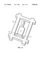
- FIG. 21is a perspective view of a probe held to a wafer with two process tabs according to the invention.
- FIG. 22is a plan view of another front side mask according to the invention.
- FIG. 23is a perspective view of another probe produced according to the invention.
- FIG. 24is a schematic side view of another probe produced according to the invention.
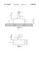
- a probe 10includes a mounting block 12 for mounting probe 10 in a scanning probe microscope, or similar instrument.
- Mounting block 12includes a bottom section 11 and a top section 13.
- a cantilever 14extends from top section 13 and terminates in a free end.
- Cantilever 14has an integral tip assembly 15 culminating in a tip 16.
- the tiphas a cone angle of preferably less than 30° and ends in a point having a diameter preferably less than 30 nm.
- cantilever 14 and tip 16are independently controlled in the production of probe 10, as will be described in detail below.
- the preferred embodimentdescribes a method for producing cantilever 14 with a thickness of 4 ⁇ m. These dimensions are for illustrative purposes only.
- the dimensions of cantilever 14 and tip 16may be varied to tailor probe 10 to a specific SPM application.
- the mounting blockhas dimensions (height ⁇ width ⁇ length) of 0.4 ⁇ 1.6 ⁇ 3.4 mm.
- probe 10is preferably produced from a silicon-on-insulator insulator (SOI) wafer 24.
- SOI wafer 24has a bottom layer 26 of single crystal silicon, a middle layer 28 of insulating material, and a top layer 30 of single crystal silicon.
- wafer 24is an n-type ⁇ 100>-oriented SOI substrate.
- wafer 24may have different orientations.
- middle layer 28is a layer of silicon dioxide. Wafer 24 may be formed by oxidizing two silicon wafers and bonding them together.
- wafer 24may be formed by implanting oxygen in a silicon wafer to form a buried oxide layer, in which case the thickness of layer 30 may be increased by silicon epitaxy.
- Specific techniques of providing a SOI waferare well known in the art.
- the specific thickness of bottom layer 26, middle layer 28, and top layer 30are selected based on the desired dimensions of probe 10.
- bottom layer 26has a preferred thickness in a range of 300 to 500 ⁇ m
- top layer 30has a preferred thickness in a range of 12 to 15 ⁇ m.
- top layer 30is selected to have a thickness that is 1 to 2 ⁇ m greater than the sum of the desired thickness of cantilever 14 and the desired height of tip assembly 15.
- top layer 30is selected in this manner to provide precise control of the dimensions of cantilever 14 and tip assembly 15, as will be explained in detail below.
- the desired thickness of cantilever 14is 4 ⁇ m and the desired height of tip assembly 15 is 6 ⁇ m so that top layer 30 is selected to have a thickness of 12 ⁇ m.
- wafer 24is bilaterally coated to form a first layer 34 of masking material on top layer 30 and a second layer 32 of masking material on bottom layer 26.
- layers 32 and 34include an outer layer of silicon nitride stacked on an inner layer of silicon dioxide.
- the outer layer of silicon nitrideis preferably 0.3 ⁇ m thick, while the inner layer of silicon dioxide is preferably 1.5 ⁇ m thick.
- the layers of silicon dioxide and silicon nitrideare deposited on wafer 24 by chemical vapor deposition (CVD).
- the layer of silicon dioxideis thermally grown on wafer 24 before the layer of silicon nitride is deposited with CVD.
- Specific techniques of coating a wafer with a layer of silicon nitride stacked on a layer of silicon dioxideare well known in the art.
- first layer 34 and second layer 32are each single layers of silicon dioxide.
- silicon nitrideis more resistant to KOH etching than silicon dioxide, so that it is preferable to include the first and second layers of silicon nitride in the masking material.
- second layer 32is patterned and etched to form a back side mask 36 on bottom layer 26.
- Back side mask 36defines a bottom mounting block pattern for forming bottom section 11 of mounting block 12.
- Back side mask 36is formed using conventional lithographic techniques well known in the art. These techniques comprise applying photoresist to layer 32 in a desired pattern of back side mask 36 and reactive ion etching layer 32 to transfer the desired pattern into layer 32.
- bottom layer 26is etched to form a bottom section 11 of mounting block 12, as shown in FIG. 4.
- Bottom layer 26is preferably etched with 25 wt. percent aqueous KOH solution at 80° C.
- bottom layer 26removes sections 38A and 38B of bottom layer 26 to form bottom section 11 of mounting block 12. Further, the etching of bottom layer 26 automatically terminates at middle layer 28. This is due to the extremely slow etching rate of silicon dioxide relative to silicon in KOH.
- This aspect of the inventionprovides a significant advantage in controlling the dimensions of both mounting block 12 and cantilever 14.
- the rate and duration of a wet chemical etchare two of the least controllable fabrication parameters in conventional methods of producing a microprobe.
- Middle layer 28eliminates the need to rely on these parameters in controlling the height of mounting block 12 and the thickness of cantilever 14.
- a tip mask pattern 40is applied to first layer 34 using conventional lithographic techniques. Such techniques, which are well known in the art, involve applying resist material to the surface, exposing the pattern, and developing the resist to leave desired pattern 40 in resist material on first layer 34. At this point in the method, the surface of first layer 34 is completely planar. Performing tip lithography on the planar surface enables tip 16 to be defined under optimal conditions. In the preferred embodiment, tip mask pattern 40 is aligned with bottom section 11 by using etch holes patterned in the top layer (not shown).
- tip mask pattern 40is aligned with bottom section 11 by using a lithography machine fitted with back side or double side alignment capability. Specific techniques of front to back side alignment are well known in the art.
- Tip mask pattern 40has a diameter D1 which corresponds to a desired diameter of the base of tip 16. In the example of the preferred embodiment diameter D1 is 1.5 ⁇ m.
- first layer 34is partially etched to form a tip mask 42, as shown in FIG. 6.
- first layer 34is partially etched by reactive ion etching in a parallel plate configuration with CHF 3 and O 2 as etch gases at a pressure in the range of 10 to 20 mT and a RF power in the range of 125 to 150W.
- the CHF 3is applied at a flow rate of 48 standard cubic centimeters per minute (sccm) and the O 2 is applied at a flow rate of 2 sccm.
- Tip mask 42is a cylindrical post having a height H1. Height H1 is selected in dependence on the desired dimensions of tip assembly 15. In the example of the preferred embodiment, height H1 is 1.25 ⁇ m.
- a front side mask 44is then produced in first layer 34.
- Front side mask 44defines a cantilever pattern and a top mounting block pattern.
- Front side mask 44is patterned using a conventional lithographic techniques.
- first layer 34is etched to form front side mask 44. In the preferred embodiment, this is done by reactive ion etching first layer 34 with CHF 3 and O 2 as etch gases at a pressure in the range of 10 to 20 mT and a RF power in the range of 125 to 150W.
- the CHF 3is applied at a flow rate of 48 sccm and the O 2 is applied at a flow rate of 2 sccm.
- FIG. 8is a cross sectional view of first layer 34, tip mask 42, and a portion of top layer 30.
- FIG. 9shows a side view of the resulting structure of wafer 24 after the step of producing front side mask 44.
- the cantilever pattern and top mounting block pattern defined by front side mask 44are transferred into layer 30, as shown in FIG. 10.
- the patternsare transferred by etching top layer 30 to a depth D2 corresponding to the desired cantilever thickness.
- depth D2is 4 ⁇ m, corresponding to the desired cantilever thickness of 4 ⁇ m.
- the transferring stepis preferably accomplished by reactive ion etching top layer 30 with Cl 2 and BCl 3 as etch gases at a pressure in the range of 30 to 40 mT and a bias voltage of 350V.
- the Cl 2is applied at a flow rate of 48 sccm and the BCl 3 is applied at a flow rate of 2 sccm.
- FIG. 11shows a side view of the resulting wafer 24 after the transferring step.
- front side mask 44is removed.
- front side mask 44is removed by reactive ion etching first layer 34 with CHF 3 and O 2 as etch gases at a pressure in the range of 10 to 20 mT and a RF power in the range of 125 to 150W.
- the CHF 3is applied at a flow rate of 48 sccm and the O 2 is applied at a flow rate of 2 sccm.
- the removal of front side mask 44leaves only tip mask 42 remaining on top layer 30, as shown in FIG. 12.
- Top layer 30is further etched to form a tip column 20, as shown in FIG. 13.
- the further etching of top layer 30also etches layer 30 to middle layer 28, thus forming cantilever 14 and top section 13 of mounting block 12.
- this etchis performed by reactive ion etching with C1 2 and BCl 3 as etch gases at a pressure 60 mT and a bias voltage of 300 V. That etch is immediately followed by a second reactive ion etch with Cl 2 and BCl 3 as etch gases at a pressure of 30 mT and a bias voltage of 350 V.
- the Cl 2is applied at a flow rate of 48 sccm and the BCl 3 is applied at a flow rate of 2 sccm.
- the etchis performed with a series of three reactive ion etches.
- the first etch in the seriesuses Cl 2 and BCl 3 as etch gases at a pressure of 30 mT.
- the second etch in the seriesuses SF 6 and O 2 as etch gases at a pressure of 100 mT.
- the third etch in the seriesuses Cl 2 and BCl 3 as etch gases at a pressure of 30 mT.
- etchantsare Cl 2 , and BCl 3 at high pressures, or SF 6 .
- top layer 30 to form cantilever 14automatically terminates at layer 28, which provides an etch stop.
- layer 28provides an etch stop.
- Thisis a very advantageous aspect of the invention, because it allows the thickness of cantilever 14 to be precisely controlled in a highly reproducible manner.
- the etchis terminated when the silicon floor is consumed. This endpoint is easily determined by visual inspection.
- cantilever 14is formed with a thickness equal to depth D2, which was previously defined in the step of transferring the cantilever pattern into top layer 30.
- Tip column 20has a height H1 equal to the selected thickness of top layer 30, less the selected thickness of cantilever 14.
- top layer 30was selected to be 12 ⁇ m thick and cantilever 14 was selected to be 4 ⁇ m thick, so that height H1 is 8 ⁇ m. This demonstrates another extremely advantageous aspect of the invention. By selecting the thickness of top layer 30, one can precisely control the thickness of cantilever 14 and height H1 of tip column 20 with a high degree of accuracy, yet still independently define both dimensions.
- tip column 20is oxidized to form tip assembly 15 having a height H2.
- height H2is 6 ⁇ m.
- height H2may be easily and precisely controlled by selecting the thickness of top layer 30 to be the sum of the desired tip height and cantilever thickness plus 1 to 2 ⁇ m. The additional thickness is consumed or pinched off during the oxidation process in a well controlled manner.
- the oxidation of tip column 20is performed at 1000° C. using H 2 at a flow rate of 4.5 l/m and O 2 at a flow rate of 2.51 l/m. In an alternative embodiment, the oxidation is performed at 1000° C.
- oxidizing tip 16uses H 2 at a flow rate of 2.25 l/m and O 2 at a flow rate of 1.25 l/m.
- Specific techniques of oxidizing tip 16are well known in the art.
- the oxidation stepproduces an oxide layer (not shown) on tip 16 and other exposed silicon surfaces.
- the oxide layeris removed in hydrofluoric acid in a manner well known in the art.
- the hydrofluoric acidalso etches the remaining portions of middle layer 28.
- the exposed portion of middle layer 28 shown in FIG. 13is removed in the hydrofluoric acid, resulting in the finished probe 10 shown in FIG. 2A.
- FIGS. 15-17A second embodiment of the invention is illustrated in FIGS. 15-17.
- the second embodiment of the inventionpresents a method for holding probe 10 in wafer 24 during production of probe 10.
- back side mask 36is modified to include process tab masks 48A and 48B prior to the step of etching bottom layer 26.
- Process tab masks 48A and 48B and back side mask 36are patterned using a conventional lithographic step of applying photoresist to second layer 32 in a desired pattern for back side mask 36 and process tabs masks 48A and 48B.
- the desired pattern of process tabs masks 48A and 48Bis transferred into second layer 32 in the same etching step used to form back side mask 36.
- Bottom layer 30is etched in same manner described in the preferred embodiment to form two process tabs 46A and 46B extending from bottom section 11 of mounting block 12, as shown in FIG. 16.
- Process tabs 46A and 46Bare for holding probe 10 in wafer 24 during the production of probe 10.
- process tabs 46A and 46Bare mechanically broken by any convenient method.
- Process tabs 46A and 46Bserve a usefutl purpose for fabricating an array of probes 10 from one wafer 24.
- a perspective view of two probes 10 held in wafer 24is shown in FIG. 17. For simplicity, only two probes 10 are shown in FIG. 17. It is obvious that a much larger number of probes 10 can be produced in wafer 24.
- the process tabsform a useful manufacturing function for fabricating an array of cantilevers/tips with uniform dimensions and high reproducibility across a wafer.
- the process tabsare important in that they enable the mounting block, cantilever and integrally formed tip to be suspended over the empty area formed by removal of the silicon wafers of the SOI wafer 24.
- the process tabsare fabricated at the thickness of the SOI wafer. They are sufficiently narrow such that the probe can be removed mechanically without danger of damage.
- the process tabsalso provide an important function in that they are rigid enough to provide mechanical support during all of the processing steps for the tip assembly.
- FIG. 18shows back side mask 36 on bottom layer 26 as in the preferred embodiment described above.
- This embodimentadds the step of producing mask patterns for edge compensation structures 50 prior to etching bottom layer 26.
- Edge compensation structures 50are for preserving the corners of bottom section 11 during the step of etching bottom layer 26 with KOH.
- Mask patterns for edge compensation structures 50are produced by conventional lithography of second layer 32 to form a desired pattern for edge compensation structures 50.
- the desired pattern for edge compensation structures 50 and back side mask 36are then transferred into second layer 32 using a reactive ion etch.
- Edge compensation structures 50are produced at an angle A relative to the latitudinal axis of back side mask 36. In the preferred embodiment, angle A is 45°.
- the etching of bottom layer 26is performed with an aqueous solution of KOH.
- Anisotropic KOHetches the higher order planes exposed at convex corners of bottom section 11 faster than it etches the low order planes on the sides of bottom section 11.
- the corners of bottom section 11may be undercut or faceted.
- the anisotropic KOH etchhas a first etch direction E1 and a second etch direction E2.
- a possible result of the anisotropic etchis an undercut corner 52 of bottom section 11. Note that faceting does not occur at concave corners.
- edge compensation structures 50preserve the corners of bottom section 11 by blocking etch direction E1 and etch direction E2.
- Each edge compensation structure 50is selected to have a width W2.
- Width W2is selected such that at the moment bottom layer 26 is etched to a desired depth, each edge compensation structure 50 is dissolved.
- width W2is 410 ⁇ m for a wafer thickness of 450 ⁇ m.
- FIG. 21A fourth embodiment of the invention is illustrated in FIG. 21.
- the fourth embodimentadvantageously combines the functions of process tabs 46A and 46B with edge compensation structures 50.
- edge compensation structure 50 emanating from the side of the mounting block opposite the cantileverare chosen to have width greater than W2 such that they will remain intact upon completion of the KOH etching.
- the width of these two edge compensation structuresis 700 ⁇ m for a wafer thickness of 450 ⁇ m.
- the resulting structures 53A and 53B in FIG. 21provide the desirable fuinctions of process tabs 46A and 46B and also prevent the two corners of mounting block 12 from being undercut during etching.
- FIGS. 22-23A fifth embodiment of the invention is illustrated in FIGS. 22-23.
- the fifth embodimentdiffers from the preferred embodiment in that cantilever 14 is produced with a free end 58 having a triangular shape, as shown in FIG. 23.
- a front side mask 54is produced on top layer 30 in the same manner as previously described in the preferred embodiment.
- front side mask 54defines a cantilever pattern 56 that differs from the cantilever pattern of the preferred embodiment.
- Cantilever pattern 56is shaped such that cantilever 14 is produced with free end 58 having a triangular shape, as shown in FIG. 23.
- the advantage of triangular shaped free end 58is that it facilities the viewing of tip 16 during the use of probe 10 in an SPM application.
- a fifth embodiment of the inventionis shown in FIG. 24.
- the fifth embodimentadds a step of coating cantilever 14 with a layer of metal 60.
- Layer of metal 60improves the reflectivity of cantilever 14 to facilitate laser scanning of cantilever 14 during its use in SPM applications.
- layer of metal 60is a layer of gold.
- layer of metal 60is a layer of aluminum or a similarly reflective metal. Specific techniques of coating cantilever 14 with layer of metal 60 are well known in the art.
- the height of the tip and cantileveris established by the thickness of the front side silicon layer of the SOI wafer. This advantageously removes reliance on timing a wet chemical etch to establish this critical dimension.
- Masking to form the tip and cantileveris performed on a surface of substantially uniform height, thereby enabling the tip diameter and cantilever width and length to be accurately established.
- Use of the preferred anisotropic etch such as plasma etchingprovides directional control over the etching process and provides accurate cuts and dimensions. Tip height and cantilever thickness are determined independently as well. Further, the cone angle and point radius of curvature are established separately from any other step. The ability to determine the dimensions of the components of the probe, especially the tip and cantilever, and the accuracy and repeatability of the method of making the probe, can result in a probe that achieves highly accurate and repeatable images of a surface to be mapped.
- the preferred embodimentdescribes a method for producing a probe having a cantilever thickness of 4 ⁇ m and a tip height of 6 ⁇ m. These dimensions are for illustrative purposes only. The dimensions of the mounting block, cantilever, and tip may be selected based on the particular application in which the probe will be used.
- the preferred embodimentdescribes using a silicon dioxide layer as the insulating layer in the SOI wafer.
- Many other materialsmay be used to form the insulating layer, such as silicon nitride, silicon carbide, or doped silicon.
- the probes produced according to the method of the inventionare not limited to use in SPM applications. The method is equally effective for producing probes for a scanning tunneling microscope, field emission assembly, and similar devices.
- the foregoing processalso can be applied to a cantilever and tip for any type of scanning probe microscopy and also to provide an array of tip assemblies which are capable of effecting a change of state or switching phenomenon in a target surface, such as an array of field emission tip assemblies.
- a target surfacesuch as an array of field emission tip assemblies.
Landscapes
- Chemical & Material Sciences (AREA)
- Engineering & Computer Science (AREA)
- Nanotechnology (AREA)
- Physics & Mathematics (AREA)
- Health & Medical Sciences (AREA)
- General Health & Medical Sciences (AREA)
- General Physics & Mathematics (AREA)
- Nuclear Medicine, Radiotherapy & Molecular Imaging (AREA)
- Radiology & Medical Imaging (AREA)
- Analytical Chemistry (AREA)
- Crystallography & Structural Chemistry (AREA)
- Length Measuring Devices With Unspecified Measuring Means (AREA)
Abstract
Description
Claims (21)
Priority Applications (1)
| Application Number | Priority Date | Filing Date | Title |
|---|---|---|---|
| US08/665,369US6066265A (en) | 1996-06-19 | 1996-06-19 | Micromachined silicon probe for scanning probe microscopy |
Applications Claiming Priority (1)
| Application Number | Priority Date | Filing Date | Title |
|---|---|---|---|
| US08/665,369US6066265A (en) | 1996-06-19 | 1996-06-19 | Micromachined silicon probe for scanning probe microscopy |
Publications (1)
| Publication Number | Publication Date |
|---|---|
| US6066265Atrue US6066265A (en) | 2000-05-23 |
Family
ID=24669850
Family Applications (1)
| Application Number | Title | Priority Date | Filing Date |
|---|---|---|---|
| US08/665,369Expired - LifetimeUS6066265A (en) | 1996-06-19 | 1996-06-19 | Micromachined silicon probe for scanning probe microscopy |
Country Status (1)
| Country | Link |
|---|---|
| US (1) | US6066265A (en) |
Cited By (56)
| Publication number | Priority date | Publication date | Assignee | Title |
|---|---|---|---|---|
| US6270685B1 (en)* | 1995-12-27 | 2001-08-07 | Denso Corporation | Method for producing a semiconductor |
| US6400166B2 (en)* | 1999-04-15 | 2002-06-04 | International Business Machines Corporation | Micro probe and method of fabricating same |
| WO2002047172A1 (en)* | 2000-12-08 | 2002-06-13 | Sophia Wireless, Inc. | A high frequency interconnect system using micromachined plugs and sockets |
| US20020135755A1 (en)* | 1994-07-28 | 2002-09-26 | Kley Victor B. | Scanning probe microscope assembly |
| US6458206B1 (en)* | 1998-05-13 | 2002-10-01 | Crystals And Technologies, Ltd. | Cantilever with whisker-grown probe and method for producing thereof |
| US6465782B1 (en)* | 1999-09-10 | 2002-10-15 | Starmega Corporation | Strongly textured atomic ridges and tip arrays |
| US6483125B1 (en) | 2001-07-13 | 2002-11-19 | North Carolina State University | Single electron transistors in which the thickness of an insulating layer defines spacing between electrodes |
| US6653653B2 (en) | 2001-07-13 | 2003-11-25 | Quantum Logic Devices, Inc. | Single-electron transistors and fabrication methods in which a projecting feature defines spacing between electrodes |
| US6673717B1 (en) | 2002-06-26 | 2004-01-06 | Quantum Logic Devices, Inc. | Methods for fabricating nanopores for single-electron devices |
| US20040038045A1 (en)* | 2001-03-26 | 2004-02-26 | Wilson Smart | Silicon penetration device with increased fracture toughness and method of fabrication |
| US20040079962A1 (en)* | 1998-10-16 | 2004-04-29 | Kabushiki Kaisha Toyota Chuo Kenkyusho | Method of manufacturing semiconductor device and semiconductor device |
| US20040118192A1 (en)* | 2002-09-09 | 2004-06-24 | General Nanotechnology Llc | Fluid delivery for scanning probe microscopy |
| US6787768B1 (en)* | 2001-03-08 | 2004-09-07 | General Nanotechnology Llc | Method and apparatus for tool and tip design for nanomachining and measurement |
| US6792804B2 (en) | 2001-10-19 | 2004-09-21 | Kionix, Inc. | Sensor for measuring out-of-plane acceleration |
| US6802646B1 (en) | 2001-04-30 | 2004-10-12 | General Nanotechnology Llc | Low-friction moving interfaces in micromachines and nanomachines |
| US20040202226A1 (en)* | 2001-10-31 | 2004-10-14 | Gianchandani Yogesh B. | Micromachined arrayed thermal probe apparatus, system for thermal scanning a sample in a contact mode and cantilevered reference probe for use therein |
| US6813937B2 (en) | 2001-11-28 | 2004-11-09 | General Nanotechnology Llc | Method and apparatus for micromachines, microstructures, nanomachines and nanostructures |
| US20040239921A1 (en)* | 2001-10-15 | 2004-12-02 | Manfred Schneegans | Probe needle for testing semiconductor chips and method for producing said probe needle |
| US20040246306A1 (en)* | 2000-02-03 | 2004-12-09 | Scott Adams | Electrostatic actuator for microelectromechanical systems and methods of fabrication |
| US20050037560A1 (en)* | 2003-07-28 | 2005-02-17 | International Business Machines Corporation | Data storage medium |
| US20050051515A1 (en)* | 2003-09-08 | 2005-03-10 | Lg Electronics Inc. | Cantilever microstructure and fabrication method thereof |
| US6865927B1 (en) | 2001-01-30 | 2005-03-15 | General Nanotechnology Llc | Sharpness testing of micro-objects such as miniature diamond tool tips |
| US20050056783A1 (en)* | 1999-07-01 | 2005-03-17 | General Nanotechnology, Llc | Object inspection and/or modification system and method |
| US6880388B1 (en) | 2001-03-08 | 2005-04-19 | General Nanotechnology Llc | Active cantilever for nanomachining and metrology |
| US20050172703A1 (en)* | 1994-07-28 | 2005-08-11 | General Nanotechnology Llc | Scanning probe microscopy inspection and modification system |
| US20050190684A1 (en)* | 1995-07-24 | 2005-09-01 | General Nanotechnology Llc | Nanometer scale data storage device and associated positioning system |
| US20050225336A1 (en)* | 2002-01-25 | 2005-10-13 | Akio Kojima | Probe card and method for manufacturing probe card |
| US20050252282A1 (en)* | 2004-05-12 | 2005-11-17 | Veeco Instruments, Inc. | Methods of fabricating structures for characterizing tip shape of scanning probe microscope probes and structures fabricated thereby |
| WO2005033650A3 (en)* | 2003-09-17 | 2005-12-08 | Zeiss Carl Nts Gmbh | Method for preparing a sample for electron microscope examination and a sample carrier and transport holder used therefor |
| US20050279729A1 (en)* | 2004-06-21 | 2005-12-22 | Veeco Instruments Inc. | Probes for use in scanning probe microscopes and methods of fabricating such probes |
| DE10344643B4 (en)* | 2003-09-17 | 2006-03-02 | Carl Zeiss Nts Gmbh | Specimen preparation method for preparing a specimen for electron microscope examinations places a specimen with a substrate in a vacuum chamber to apply a coating and ion beam |
| US20060076488A1 (en)* | 2004-10-12 | 2006-04-13 | Hideki Ina | Surface shape measuring apparatus, surface measuring method, and exposure apparatus |
| US7053369B1 (en) | 2001-10-19 | 2006-05-30 | Rave Llc | Scan data collection for better overall data accuracy |
| WO2004113868A3 (en)* | 2003-06-17 | 2006-06-08 | Wisconsin Alumni Res Found | Samples for atom probes and method of producing the same |
| US20060213259A1 (en)* | 2004-09-23 | 2006-09-28 | Prinz Friedrich B | Sensors for electrochemical, electrical or topographical analysis |
| US7178387B1 (en) | 2001-03-08 | 2007-02-20 | General Nanotechnology Llc | Method and apparatus for scanning in scanning probe microscopy and presenting results |
| US20070044545A1 (en)* | 2005-08-19 | 2007-03-01 | Arthur Beyder | Oscillator and method of making for atomic force microscope and other applications |
| US20070125160A1 (en)* | 2005-11-15 | 2007-06-07 | The University Of Houston | Short and thin silicon cantilever with tip and fabrication thereof |
| US20070145966A1 (en)* | 2003-11-25 | 2007-06-28 | Gajendra Shekhawat | Cascaded mosfet embedded multi-input microcantilever |
| US7253407B1 (en) | 2001-03-08 | 2007-08-07 | General Nanotechnology Llc | Active cantilever for nanomachining and metrology |
| US20090031792A1 (en)* | 2007-08-02 | 2009-02-05 | Wenjun Fan | Probe Device for a Metrology Instrument and Method of Fabricating the Same |
| JP2009031038A (en)* | 2007-07-25 | 2009-02-12 | Ritsumeikan | Probe, probe forming etching mask, and probe manufacturing method using the same |
| US7494593B1 (en) | 2004-06-28 | 2009-02-24 | Hewlett-Packard Development Company, L.P. | Method for forming a cantilever and tip |
| US20090239205A1 (en)* | 2006-11-16 | 2009-09-24 | Morgia Michael A | System And Method For Algorithmic Selection Of A Consensus From A Plurality Of Ideas |
| US7947952B1 (en) | 2001-03-08 | 2011-05-24 | General Nanotechnology Llc | Nanomachining method and apparatus |
| US8479309B2 (en) | 2011-04-28 | 2013-07-02 | The Board Of Trustees Of The University Of Illinois | Ultra-low damping imaging mode related to scanning probe microscopy in liquid |
| US8539611B1 (en)* | 2012-07-02 | 2013-09-17 | International Business Machines Corporation | Scanned probe microscopy (SPM) probe having angled tip |
| US8726411B1 (en)* | 2013-03-21 | 2014-05-13 | National Tsing Hua University | Charged probe and electric fields measurement method thereof |
| CN112986622A (en)* | 2021-03-02 | 2021-06-18 | 中国科学院半导体研究所 | Wafer-level nanometer needle tip and manufacturing method thereof |
| CN114638107A (en)* | 2022-03-21 | 2022-06-17 | 中国科学院微电子研究所 | Atomic layer etching process simulation method and device of multi-lamination structure |
| WO2022130353A1 (en)* | 2020-12-20 | 2022-06-23 | СканСенс ГмбХ | Cantilever with a silicon tip |
| CN116079706A (en)* | 2021-11-08 | 2023-05-09 | 港大科桥有限公司 | Nanorobotic system for high-throughput single-cell DNA sequencing |
| CN116519979A (en)* | 2023-05-23 | 2023-08-01 | 中国科学院苏州纳米技术与纳米仿生研究所 | Cantilever probe of atomic force microscope and manufacturing method thereof |
| US12091313B2 (en) | 2019-08-26 | 2024-09-17 | The Research Foundation For The State University Of New York | Electrodynamically levitated actuator |
| US12103843B2 (en) | 2021-01-20 | 2024-10-01 | Calient.Ai Inc. | MEMS mirror arrays with reduced crosstalk |
| EP4513201A1 (en)* | 2023-08-21 | 2025-02-26 | Imec VZW | A method for producing a substrate comprising scanning probe microscopy tips |
Citations (10)
| Publication number | Priority date | Publication date | Assignee | Title |
|---|---|---|---|---|
| US4968585A (en)* | 1989-06-20 | 1990-11-06 | The Board Of Trustees Of The Leland Stanford Jr. University | Microfabricated cantilever stylus with integrated conical tip |
| US5066358A (en)* | 1988-10-27 | 1991-11-19 | Board Of Trustees Of The Leland Stanford Juninor University | Nitride cantilevers with single crystal silicon tips |
| US5116462A (en)* | 1989-08-16 | 1992-05-26 | International Business Machines Corporation | Method of producing micromechanical sensors for the afm/stm profilometry |
| US5201992A (en)* | 1990-07-12 | 1993-04-13 | Bell Communications Research, Inc. | Method for making tapered microminiature silicon structures |
| US5242541A (en)* | 1989-08-16 | 1993-09-07 | International Business Machines Corporation | Method of producing ultrafine silicon tips for the afm/stm profilometry |
| US5282924A (en)* | 1990-07-25 | 1994-02-01 | International Business Machines Corporation | Micromechanical sensor fabrication process |
| US5286343A (en)* | 1992-07-24 | 1994-02-15 | Regents Of The University Of California | Method for protecting chip corners in wet chemical etching of wafers |
| US5313451A (en)* | 1990-04-18 | 1994-05-17 | Canon Kabushiki Kaisha | Information recording/reproducing apparatus with STM cantilever probe having a strain gauge |
| US5354985A (en)* | 1993-06-03 | 1994-10-11 | Stanford University | Near field scanning optical and force microscope including cantilever and optical waveguide |
| US5396066A (en)* | 1992-07-06 | 1995-03-07 | Canon Kabushiki Kaisha | Displacement element, cantilever probe and information processing apparatus using cantilever probe |
- 1996
- 1996-06-19USUS08/665,369patent/US6066265A/ennot_activeExpired - Lifetime
Patent Citations (11)
| Publication number | Priority date | Publication date | Assignee | Title |
|---|---|---|---|---|
| US5066358A (en)* | 1988-10-27 | 1991-11-19 | Board Of Trustees Of The Leland Stanford Juninor University | Nitride cantilevers with single crystal silicon tips |
| US4968585A (en)* | 1989-06-20 | 1990-11-06 | The Board Of Trustees Of The Leland Stanford Jr. University | Microfabricated cantilever stylus with integrated conical tip |
| US5116462A (en)* | 1989-08-16 | 1992-05-26 | International Business Machines Corporation | Method of producing micromechanical sensors for the afm/stm profilometry |
| US5242541A (en)* | 1989-08-16 | 1993-09-07 | International Business Machines Corporation | Method of producing ultrafine silicon tips for the afm/stm profilometry |
| US5313451A (en)* | 1990-04-18 | 1994-05-17 | Canon Kabushiki Kaisha | Information recording/reproducing apparatus with STM cantilever probe having a strain gauge |
| US5201992A (en)* | 1990-07-12 | 1993-04-13 | Bell Communications Research, Inc. | Method for making tapered microminiature silicon structures |
| US5282924A (en)* | 1990-07-25 | 1994-02-01 | International Business Machines Corporation | Micromechanical sensor fabrication process |
| US5455419A (en)* | 1990-07-25 | 1995-10-03 | International Business Machines Corporation | Micromechanical sensor and sensor fabrication process |
| US5396066A (en)* | 1992-07-06 | 1995-03-07 | Canon Kabushiki Kaisha | Displacement element, cantilever probe and information processing apparatus using cantilever probe |
| US5286343A (en)* | 1992-07-24 | 1994-02-15 | Regents Of The University Of California | Method for protecting chip corners in wet chemical etching of wafers |
| US5354985A (en)* | 1993-06-03 | 1994-10-11 | Stanford University | Near field scanning optical and force microscope including cantilever and optical waveguide |
Non-Patent Citations (24)
| Title |
|---|
| Andrew Pember, "Study of the Effect of Boron Doping on the Aging of Micromachined Silicon Cantilevers", Appl. Physics, Lett. 66, pp. 577-579, Jan. 1995. |
| Andrew Pember, Study of the Effect of Boron Doping on the Aging of Micromachined Silicon Cantilevers , Appl. Physics, Lett. 66, pp. 577 579, Jan. 1995.* |
| G.K. Mayer, "Fabrication of Non-Underetched Convex Corners in Anisotropic Etching of (100)-Silicon in Aqueous KOH with Respect to Novel Micromechanic Element", J. Elecrochem, Soc. vol. 137, No. 12, pp. 3947-3951, Dec. 1990. |
| G.K. Mayer, Fabrication of Non Underetched Convex Corners in Anisotropic Etching of (100) Silicon in Aqueous KOH with Respect to Novel Micromechanic Element , J. Elecrochem, Soc. vol. 137, No. 12, pp. 3947 3951, Dec. 1990.* |
| H.L. Offereins, "Methods for the Fabrication of Convex Corners in Anisotropic Etching of (100) Silicon in Aqueous KOH", Sensors and Actuators A, pp. 9-13, 1991. |
| H.L. Offereins, Methods for the Fabrication of Convex Corners in Anisotropic Etching of (100) Silicon in Aqueous KOH , Sensors and Actuators A, pp. 9 13, 1991.* |
| J.A.Dagata, "Device Fabrication by Scanned Probe Oxidation", Science, vol. 270, pp. 1625-1641, Dec. 8, 1995. |
| J.A.Dagata, Device Fabrication by Scanned Probe Oxidation , Science, vol. 270, pp. 1625 1641, Dec. 8, 1995.* |
| J.Lai, "Thermal Detection of Device Failure by Atomic Force Microscopy", IEEE Trans. Devices, vol. 16, No. 7, Jul. 1995. |
| J.Lai, Thermal Detection of Device Failure by Atomic Force Microscopy , IEEE Trans. Devices, vol. 16, No. 7, Jul. 1995.* |
| Joseph E. Griffith, "Dimensional Metrology with Scanning Probe Microscopes", J.Appl.Physics 74, pp. R83-R109, Nov. 1, 1993. |
| Joseph E. Griffith, Dimensional Metrology with Scanning Probe Microscopes , J.Appl.Physics 74, pp. R83 R109, Nov. 1, 1993.* |
| Junji Itoh, "Fabricationn of an Ultrasharp and High-Aspect-Ratio Microprobe with a Silicon-on-Insulator Wafer for Scanning Force Microscopy", pp. 331-334, Dec. 1994. |
| Junji Itoh, Fabricationn of an Ultrasharp and High Aspect Ratio Microprobe with a Silicon on Insulator Wafer for Scanning Force Microscopy , pp. 331 334, Dec. 1994.* |
| Kenneth E. Bean, "Anisotropic Etching of Silicon", IEEE Trans. Devices, vol. ED-25, No. 10, pp. 1185-1193, Oct. 1978. |
| Kenneth E. Bean, Anisotropic Etching of Silicon , IEEE Trans. Devices, vol. ED 25, No. 10, pp. 1185 1193, Oct. 1978.* |
| R.B.Protsch, "Magnetic Force Microscopy of the Submicron Magnetic Assembly in a Magnetotactic Bacterium", Appl. Physics Lett 66, pp. 2852-2854, May 8, 1995. |
| R.B.Protsch, Magnetic Force Microscopy of the Submicron Magnetic Assembly in a Magnetotactic Bacterium , Appl. Physics Lett 66, pp. 2852 2854, May 8, 1995.* |
| S.C.Minne, "Parallel Atomic Force Microscopy using Cantilevers with Integrated Piezoresistive Sensors and Integrated Piezoeletric Actuators", Appl. Physics Lett. 67, pp. 3918-3920, Dec. 25, 1995. |
| S.C.Minne, Parallel Atomic Force Microscopy using Cantilevers with Integrated Piezoresistive Sensors and Integrated Piezoeletric Actuators , Appl. Physics Lett. 67, pp. 3918 3920, Dec. 25, 1995.* |
| S.R.Manalis, "Atomic Force Microscopy of High Speed Imaging Using Cantilevers with an Integrated Actuator and Sensor", Appl. Physics Lett. 68, pp. 871-873, Feb. 5, 1996. |
| S.R.Manalis, Atomic Force Microscopy of High Speed Imaging Using Cantilevers with an Integrated Actuator and Sensor , Appl. Physics Lett. 68, pp. 871 873, Feb. 5, 1996.* |
| Xian Ping Wu, Compensating Corner Undercutting in Anisotropic Etching of (100) Silicon , Sensors and Actuator, vol. 18, pp. 207 215, 1989.* |
| Xian-Ping Wu, "Compensating Corner Undercutting in Anisotropic Etching of (100) Silicon", Sensors and Actuator, vol. 18, pp. 207-215, 1989. |
Cited By (109)
| Publication number | Priority date | Publication date | Assignee | Title |
|---|---|---|---|---|
| US20060237639A1 (en)* | 1994-07-28 | 2006-10-26 | General Nanotechnology Llc | Scanning probe microscope assembly and method for making spectrophotometric, near-filed, and scanning probe measurements |
| US7615738B2 (en) | 1994-07-28 | 2009-11-10 | General Nanotechnology, Llc | Scanning probe microscope assembly and method for making spectrophotometric, near-field, and scanning probe measurements |
| US7091476B2 (en) | 1994-07-28 | 2006-08-15 | General Nanotechnology Llc | Scanning probe microscope assembly |
| US20020135755A1 (en)* | 1994-07-28 | 2002-09-26 | Kley Victor B. | Scanning probe microscope assembly |
| US20050172703A1 (en)* | 1994-07-28 | 2005-08-11 | General Nanotechnology Llc | Scanning probe microscopy inspection and modification system |
| US7045780B2 (en) | 1994-07-28 | 2006-05-16 | General Nanotechnology, Llc | Scanning probe microscopy inspection and modification system |
| US20070022804A1 (en)* | 1994-07-28 | 2007-02-01 | General Nanotechnology Llc | Scanning probe microscopy inspection and modification system |
| US7485856B2 (en) | 1994-07-28 | 2009-02-03 | General Nanotechnology Llp | Scanning probe microscopy inspection and modification system |
| US7535817B2 (en) | 1995-07-24 | 2009-05-19 | General Nanotechnology, L.L.C. | Nanometer scale data storage device and associated positioning system |
| US20050190684A1 (en)* | 1995-07-24 | 2005-09-01 | General Nanotechnology Llc | Nanometer scale data storage device and associated positioning system |
| US7042828B2 (en) | 1995-07-24 | 2006-05-09 | General Nanotechnology Llc | Nanometer scale data storage device and associated positioning system |
| US20060239129A1 (en)* | 1995-07-24 | 2006-10-26 | General Nanotechnology Llc | Nanometer scale data storage device and associated positioning system |
| US6270685B1 (en)* | 1995-12-27 | 2001-08-07 | Denso Corporation | Method for producing a semiconductor |
| US10610995B2 (en) | 1998-01-21 | 2020-04-07 | Victor B. Kley | Method and apparatus for nanolapping |
| US6458206B1 (en)* | 1998-05-13 | 2002-10-01 | Crystals And Technologies, Ltd. | Cantilever with whisker-grown probe and method for producing thereof |
| US6936484B2 (en) | 1998-10-16 | 2005-08-30 | Kabushiki Kaisha Toyota Chuo Kenkyusho | Method of manufacturing semiconductor device and semiconductor device |
| US20040079962A1 (en)* | 1998-10-16 | 2004-04-29 | Kabushiki Kaisha Toyota Chuo Kenkyusho | Method of manufacturing semiconductor device and semiconductor device |
| US6400166B2 (en)* | 1999-04-15 | 2002-06-04 | International Business Machines Corporation | Micro probe and method of fabricating same |
| US7109482B2 (en) | 1999-07-01 | 2006-09-19 | General Nanotechnology Llc | Object inspection and/or modification system and method |
| US20050056783A1 (en)* | 1999-07-01 | 2005-03-17 | General Nanotechnology, Llc | Object inspection and/or modification system and method |
| US6465782B1 (en)* | 1999-09-10 | 2002-10-15 | Starmega Corporation | Strongly textured atomic ridges and tip arrays |
| US20040246306A1 (en)* | 2000-02-03 | 2004-12-09 | Scott Adams | Electrostatic actuator for microelectromechanical systems and methods of fabrication |
| US7098571B2 (en) | 2000-02-03 | 2006-08-29 | Calient Networks, Inc. | Electrostatic actuator for microelectromechanical systems and methods of fabrication |
| US7261826B2 (en) | 2000-02-03 | 2007-08-28 | Calient Networks, Inc. | Electrostatic actuator for microelectromechanical systems and methods of fabrication |
| WO2002047172A1 (en)* | 2000-12-08 | 2002-06-13 | Sophia Wireless, Inc. | A high frequency interconnect system using micromachined plugs and sockets |
| US6865927B1 (en) | 2001-01-30 | 2005-03-15 | General Nanotechnology Llc | Sharpness testing of micro-objects such as miniature diamond tool tips |
| US6931710B2 (en) | 2001-01-30 | 2005-08-23 | General Nanotechnology Llc | Manufacturing of micro-objects such as miniature diamond tool tips |
| US20050115047A1 (en)* | 2001-01-30 | 2005-06-02 | General Nanotechnology Llc | Manufacturing of micro-objects such as miniature diamond tool tips |
| US6880388B1 (en) | 2001-03-08 | 2005-04-19 | General Nanotechnology Llc | Active cantilever for nanomachining and metrology |
| US6923044B1 (en) | 2001-03-08 | 2005-08-02 | General Nanotechnology Llc | Active cantilever for nanomachining and metrology |
| US7253407B1 (en) | 2001-03-08 | 2007-08-07 | General Nanotechnology Llc | Active cantilever for nanomachining and metrology |
| US7178387B1 (en) | 2001-03-08 | 2007-02-20 | General Nanotechnology Llc | Method and apparatus for scanning in scanning probe microscopy and presenting results |
| US6787768B1 (en)* | 2001-03-08 | 2004-09-07 | General Nanotechnology Llc | Method and apparatus for tool and tip design for nanomachining and measurement |
| US7947952B1 (en) | 2001-03-08 | 2011-05-24 | General Nanotechnology Llc | Nanomachining method and apparatus |
| US7137292B1 (en) | 2001-03-08 | 2006-11-21 | General Nanotechnology Llc | Active cantilever for nanomachining and metrology |
| US6852365B2 (en)* | 2001-03-26 | 2005-02-08 | Kumetrix, Inc. | Silicon penetration device with increased fracture toughness and method of fabrication |
| US20040038045A1 (en)* | 2001-03-26 | 2004-02-26 | Wilson Smart | Silicon penetration device with increased fracture toughness and method of fabrication |
| US6802646B1 (en) | 2001-04-30 | 2004-10-12 | General Nanotechnology Llc | Low-friction moving interfaces in micromachines and nanomachines |
| US20050058384A1 (en)* | 2001-04-30 | 2005-03-17 | General Nanotechnology Llc | Low-friction moving interfaces in micromachines and nanomachines |
| US6784082B2 (en) | 2001-07-13 | 2004-08-31 | North Carolina State University | Methods of fabricating single electron transistors in which the thickness of an insulating layer defines spacing between electrodes |
| US6653653B2 (en) | 2001-07-13 | 2003-11-25 | Quantum Logic Devices, Inc. | Single-electron transistors and fabrication methods in which a projecting feature defines spacing between electrodes |
| US6483125B1 (en) | 2001-07-13 | 2002-11-19 | North Carolina State University | Single electron transistors in which the thickness of an insulating layer defines spacing between electrodes |
| US7212019B2 (en)* | 2001-10-15 | 2007-05-01 | Infineon Technologies Ag | Probe needle for testing semiconductor chips and method for producing said probe needle |
| US20040239921A1 (en)* | 2001-10-15 | 2004-12-02 | Manfred Schneegans | Probe needle for testing semiconductor chips and method for producing said probe needle |
| US7547882B2 (en) | 2001-10-19 | 2009-06-16 | Rave Llc | Scan data collection for better overall data accurancy |
| US7053369B1 (en) | 2001-10-19 | 2006-05-30 | Rave Llc | Scan data collection for better overall data accuracy |
| US20060174384A1 (en)* | 2001-10-19 | 2006-08-03 | Rave Llc | Scan data collection for better overall data accurancy |
| US6792804B2 (en) | 2001-10-19 | 2004-09-21 | Kionix, Inc. | Sensor for measuring out-of-plane acceleration |
| US7073938B2 (en)* | 2001-10-31 | 2006-07-11 | The Regents Of The University Of Michigan | Micromachined arrayed thermal probe apparatus, system for thermal scanning a sample in a contact mode and cantilevered reference probe for use therein |
| US20040202226A1 (en)* | 2001-10-31 | 2004-10-14 | Gianchandani Yogesh B. | Micromachined arrayed thermal probe apparatus, system for thermal scanning a sample in a contact mode and cantilevered reference probe for use therein |
| US7631549B1 (en) | 2001-11-28 | 2009-12-15 | General Nanotechnology Llc | Method and apparatus for micromachines, microstructures, nanomachines and nanostructures |
| US20050172739A1 (en)* | 2001-11-28 | 2005-08-11 | General Nanotechnology Llc | Method and apparatus for micromachines, microstructures, nanomachines and nanostructures |
| US6813937B2 (en) | 2001-11-28 | 2004-11-09 | General Nanotechnology Llc | Method and apparatus for micromachines, microstructures, nanomachines and nanostructures |
| US7266998B2 (en) | 2001-11-28 | 2007-09-11 | General Nanotechnology Llc | Method and apparatus for micromachines, microstructures, nanomachines and nanostructures |
| US7394265B2 (en)* | 2002-01-25 | 2008-07-01 | Advantest Corp. | Flat portions of a probe card flattened to have same vertical level with one another by compensating the unevenness of a substrate and each identical height needle being mounted on the corresponding flat portion through an adhesive |
| US20050225336A1 (en)* | 2002-01-25 | 2005-10-13 | Akio Kojima | Probe card and method for manufacturing probe card |
| US9075082B2 (en) | 2002-03-07 | 2015-07-07 | Victor B. Kley | Fluid delivery for scanning probe microscopy |
| US6673717B1 (en) | 2002-06-26 | 2004-01-06 | Quantum Logic Devices, Inc. | Methods for fabricating nanopores for single-electron devices |
| US20120066800A1 (en)* | 2002-09-09 | 2012-03-15 | General Nanotechnology LLC. | Fluid delivery for scanning probe microscopy |
| US20040118192A1 (en)* | 2002-09-09 | 2004-06-24 | General Nanotechnology Llc | Fluid delivery for scanning probe microscopy |
| WO2004113868A3 (en)* | 2003-06-17 | 2006-06-08 | Wisconsin Alumni Res Found | Samples for atom probes and method of producing the same |
| US7336591B2 (en)* | 2003-07-28 | 2008-02-26 | International Business Machines Corporation | Data storage medium |
| US20050037560A1 (en)* | 2003-07-28 | 2005-02-17 | International Business Machines Corporation | Data storage medium |
| US20050051515A1 (en)* | 2003-09-08 | 2005-03-10 | Lg Electronics Inc. | Cantilever microstructure and fabrication method thereof |
| US7182876B2 (en)* | 2003-09-08 | 2007-02-27 | Lg Electronics Inc. | Cantilever microstructure and fabrication method thereof |
| US7375325B2 (en) | 2003-09-17 | 2008-05-20 | Carl Zeiss Nts Gmbh | Method for preparing a sample for electron microscopic examinations, and sample supports and transport holders used therefor |
| WO2005033650A3 (en)* | 2003-09-17 | 2005-12-08 | Zeiss Carl Nts Gmbh | Method for preparing a sample for electron microscope examination and a sample carrier and transport holder used therefor |
| EP1818970A3 (en)* | 2003-09-17 | 2009-09-16 | Carl Zeiss NTS GmbH | Method for preparing a sample for electron microscopic investigation, the sample carrier and transport carrier used |
| DE10344643B4 (en)* | 2003-09-17 | 2006-03-02 | Carl Zeiss Nts Gmbh | Specimen preparation method for preparing a specimen for electron microscope examinations places a specimen with a substrate in a vacuum chamber to apply a coating and ion beam |
| US20070145966A1 (en)* | 2003-11-25 | 2007-06-28 | Gajendra Shekhawat | Cascaded mosfet embedded multi-input microcantilever |
| US7759924B2 (en)* | 2003-11-25 | 2010-07-20 | Northwestern University | Cascaded MOSFET embedded multi-input microcantilever |
| WO2005069802A3 (en)* | 2004-01-19 | 2006-01-26 | Univ Michigan | Micromachined arrayed thermal probe apparatus and system for thermal scanning |
| US7096711B2 (en)* | 2004-05-12 | 2006-08-29 | Veeco Instruments Inc. | Methods of fabricating structures for characterizing tip shape of scanning probe microscope probes and structures fabricated thereby |
| US20050252282A1 (en)* | 2004-05-12 | 2005-11-17 | Veeco Instruments, Inc. | Methods of fabricating structures for characterizing tip shape of scanning probe microscope probes and structures fabricated thereby |
| US7210330B2 (en) | 2004-05-12 | 2007-05-01 | Veeco Instruments, Inc. | Methods of fabricating structures for characterizing tip shape of scanning probe microscope probes and structures fabricated thereby |
| US20060277972A1 (en)* | 2004-05-12 | 2006-12-14 | Veeco Instruments Inc. | Methods of fabricating structures for characterizing tip shape of scanning probe microscope probes and structures fabricated thereby |
| US7370515B2 (en) | 2004-06-21 | 2008-05-13 | Veeco Instruments Inc. | Probes for use in scanning probe microscopes and methods of fabricating such probes |
| US20050279729A1 (en)* | 2004-06-21 | 2005-12-22 | Veeco Instruments Inc. | Probes for use in scanning probe microscopes and methods of fabricating such probes |
| WO2006002153A1 (en)* | 2004-06-21 | 2006-01-05 | Veeco Instruments, Inc. | Probes for use in scanning probe microscopes and methods of fabricating such probes |
| US7494593B1 (en) | 2004-06-28 | 2009-02-24 | Hewlett-Packard Development Company, L.P. | Method for forming a cantilever and tip |
| US20060213259A1 (en)* | 2004-09-23 | 2006-09-28 | Prinz Friedrich B | Sensors for electrochemical, electrical or topographical analysis |
| US7444856B2 (en)* | 2004-09-23 | 2008-11-04 | The Board Of Trustees Of The Leland Stanford Junior University | Sensors for electrochemical, electrical or topographical analysis |
| US20060076488A1 (en)* | 2004-10-12 | 2006-04-13 | Hideki Ina | Surface shape measuring apparatus, surface measuring method, and exposure apparatus |
| US7497111B2 (en)* | 2004-10-12 | 2009-03-03 | Canon Kabushiki Kaisha | Surface shape measuring apparatus, surface measuring method, and exposure apparatus |
| US20070044545A1 (en)* | 2005-08-19 | 2007-03-01 | Arthur Beyder | Oscillator and method of making for atomic force microscope and other applications |
| US7340944B2 (en) | 2005-08-19 | 2008-03-11 | Arthur Beyder | Oscillator and method of making for atomic force microscope and other applications |
| US7533561B2 (en) | 2005-08-19 | 2009-05-19 | Arthur Beyder | Oscillator for atomic force microscope and other applications |
| US20070062265A1 (en)* | 2005-08-19 | 2007-03-22 | Arthur Beyder | Oscillator for atomic force microscope and other applications |
| US7637960B2 (en)* | 2005-11-15 | 2009-12-29 | University Of Houston | Short and thin silicon cantilever with tip and fabrication thereof |
| US20070125160A1 (en)* | 2005-11-15 | 2007-06-07 | The University Of Houston | Short and thin silicon cantilever with tip and fabrication thereof |
| US20090239205A1 (en)* | 2006-11-16 | 2009-09-24 | Morgia Michael A | System And Method For Algorithmic Selection Of A Consensus From A Plurality Of Ideas |
| US8494436B2 (en) | 2006-11-16 | 2013-07-23 | Watertown Software, Inc. | System and method for algorithmic selection of a consensus from a plurality of ideas |
| JP2009031038A (en)* | 2007-07-25 | 2009-02-12 | Ritsumeikan | Probe, probe forming etching mask, and probe manufacturing method using the same |
| WO2009018571A3 (en)* | 2007-08-02 | 2009-03-26 | Veeco Instr Inc | Probe device for a metrology instrument and method of fabricating the same |
| US7823216B2 (en) | 2007-08-02 | 2010-10-26 | Veeco Instruments Inc. | Probe device for a metrology instrument and method of fabricating the same |
| US20090031792A1 (en)* | 2007-08-02 | 2009-02-05 | Wenjun Fan | Probe Device for a Metrology Instrument and Method of Fabricating the Same |
| US8479309B2 (en) | 2011-04-28 | 2013-07-02 | The Board Of Trustees Of The University Of Illinois | Ultra-low damping imaging mode related to scanning probe microscopy in liquid |
| US8893310B2 (en) | 2012-07-02 | 2014-11-18 | International Business Machines Corporation | Scanned probe microscopy (SPM) probe having angled tip |
| US8539611B1 (en)* | 2012-07-02 | 2013-09-17 | International Business Machines Corporation | Scanned probe microscopy (SPM) probe having angled tip |
| US8726411B1 (en)* | 2013-03-21 | 2014-05-13 | National Tsing Hua University | Charged probe and electric fields measurement method thereof |
| US12091313B2 (en) | 2019-08-26 | 2024-09-17 | The Research Foundation For The State University Of New York | Electrodynamically levitated actuator |
| WO2022130353A1 (en)* | 2020-12-20 | 2022-06-23 | СканСенс ГмбХ | Cantilever with a silicon tip |
| US12103843B2 (en) | 2021-01-20 | 2024-10-01 | Calient.Ai Inc. | MEMS mirror arrays with reduced crosstalk |
| CN112986622A (en)* | 2021-03-02 | 2021-06-18 | 中国科学院半导体研究所 | Wafer-level nanometer needle tip and manufacturing method thereof |
| CN112986622B (en)* | 2021-03-02 | 2023-03-14 | 中国科学院半导体研究所 | Wafer-level nanometer needle tip and manufacturing method thereof |
| CN116079706A (en)* | 2021-11-08 | 2023-05-09 | 港大科桥有限公司 | Nanorobotic system for high-throughput single-cell DNA sequencing |
| CN114638107A (en)* | 2022-03-21 | 2022-06-17 | 中国科学院微电子研究所 | Atomic layer etching process simulation method and device of multi-lamination structure |
| CN116519979A (en)* | 2023-05-23 | 2023-08-01 | 中国科学院苏州纳米技术与纳米仿生研究所 | Cantilever probe of atomic force microscope and manufacturing method thereof |
| EP4513201A1 (en)* | 2023-08-21 | 2025-02-26 | Imec VZW | A method for producing a substrate comprising scanning probe microscopy tips |
Similar Documents
| Publication | Publication Date | Title |
|---|---|---|
| US6066265A (en) | Micromachined silicon probe for scanning probe microscopy | |
| EP0413042B1 (en) | Method of producing micromechanical sensors for the afm/stm profilometry and micromechanical afm/stm sensor head | |
| US5811017A (en) | Cantilever for use in a scanning probe microscope and method of manufacturing the same | |
| EP0468071B1 (en) | Method of producing micromechanical sensors for the AFM/STM/MFM profilometry and micromechanical AFM/STM/MFM sensor head | |
| US5116462A (en) | Method of producing micromechanical sensors for the afm/stm profilometry | |
| EP0413040B1 (en) | Method of producing ultrafine silicon tips for the afm/stm profilometry | |
| US5578745A (en) | Calibration standards for profilometers and methods of producing them | |
| US5272913A (en) | Cantilever for a scanning probe microscope and a method of manufacturing the same | |
| Grow et al. | Silicon nitride cantilevers with oxidation-sharpened silicon tips for atomic force microscopy | |
| US8397555B1 (en) | Scanning probe devices | |
| US8828243B2 (en) | Scanning probe having integrated silicon tip with cantilever | |
| US6415653B1 (en) | Cantilever for use in a scanning probe microscope | |
| Rangelow et al. | Fabrication of piezoresistive-sensed AFM cantilever probe with integrated tip | |
| JP5249245B2 (en) | A probe capable of video rates for atomic force microscopy | |
| Itoh et al. | Fabrication of an ultrasharp and high‐aspect‐ratio microprobe with a silicon‐on‐insulator wafer for scanning force microscopy | |
| KR20010003182A (en) | Fabrication method of SPM probe tips using P+ silicon cantilevers realized in <110>bulk silicon wafer | |
| Kassing et al. | Sensors for scanning probe microscopy | |
| EP1061529A1 (en) | A probe tip for the investigation of a substrate and a method of fabrication therof | |
| JPH09152436A (en) | Probe for scanning probe microscope and making thereof | |
| US7861315B2 (en) | Method for microfabricating a probe with integrated handle, cantilever, tip and circuit | |
| JPH05256643A (en) | Cantilever chip for scanning type probe microscope | |
| WO2003087709A1 (en) | Nanowire microscope probe tips | |
| JPH11337562A (en) | Cantilever for scanning type probe microscope | |
| JPH10339736A (en) | Probe for scanning type probe microscope and producing method therefor | |
| JPH11337563A (en) | Manufacture of cantilever for scanning type probe microscope |
Legal Events
| Date | Code | Title | Description |
|---|---|---|---|
| AS | Assignment | Owner name:TMS TECHNOLOGIES, INC., NEW YORK Free format text:ASSIGNMENT OF ASSIGNORS INTEREST;ASSIGNORS:GALVIN, GREGORY J,;DAVIS, TIMOTHY J.;REEL/FRAME:008314/0172 Effective date:19961004 | |
| AS | Assignment | Owner name:KIONIX, INC., NEW YORK Free format text:CHANGE OF NAME;ASSIGNOR:TMS TECHNOLOGIES, INC.;REEL/FRAME:010042/0395 Effective date:19971217 | |
| STCF | Information on status: patent grant | Free format text:PATENTED CASE | |
| AS | Assignment | Owner name:VENTURE LENDING & LEASING III, INC., AS AGENT, CAL Free format text:SECURITY AGREEMENT;ASSIGNOR:CALIENT OPTICAL COMPONENTS, INC.;REEL/FRAME:011934/0464 Effective date:20010516 | |
| AS | Assignment | Owner name:PENTECH FINANCIAL SERVICES, INC., CALIFORNIA Free format text:SECURITY INTEREST;ASSIGNOR:CALIENT OPTICAL COMPONENTS, INC.;REEL/FRAME:012252/0175 Effective date:20010516 | |
| AS | Assignment | Owner name:BARTELS, HENRY, CONNECTICUT Free format text:SECURITY AGREEMENT;ASSIGNOR:CALIENT OPTICAL COMPONENTS, INC.;REEL/FRAME:014172/0551 Effective date:20031110 Owner name:BARTELS, KENNETH G., CONNECTICUT Free format text:SECURITY AGREEMENT;ASSIGNOR:CALIENT OPTICAL COMPONENTS, INC.;REEL/FRAME:014172/0551 Effective date:20031110 Owner name:BARTELS, PHILIP H., CONNECTICUT Free format text:SECURITY AGREEMENT;ASSIGNOR:CALIENT OPTICAL COMPONENTS, INC.;REEL/FRAME:014172/0551 Effective date:20031110 Owner name:CAYUGA VENTURE FUND II LLC AS AGENT, NEW YORK Free format text:SECURITY AGREEMENT;ASSIGNOR:CALIENT OPTICAL COMPONENTS, INC.;REEL/FRAME:014172/0551 Effective date:20031110 Owner name:PENTECH FINANCIAL SERVICES, INC., CALIFORNIA Free format text:RELEASE BY ASSIGNMENT AND ASSUMPTION AGREEMENT;ASSIGNORS:CAYUGA VENTURE FUND II, LLC AS AGENT;SHULL, ARTHUR;WIDDING, FRED B.;AND OTHERS;REEL/FRAME:014172/0676 Effective date:20031110 Owner name:SHULL, ARTHUR, NEW YORK Free format text:SECURITY AGREEMENT;ASSIGNOR:CALIENT OPTICAL COMPONENTS, INC.;REEL/FRAME:014172/0551 Effective date:20031110 Owner name:WIDDING, FRED B., NEW YORK Free format text:SECURITY AGREEMENT;ASSIGNOR:CALIENT OPTICAL COMPONENTS, INC.;REEL/FRAME:014172/0551 Effective date:20031110 | |
| FEPP | Fee payment procedure | Free format text:PAT HOLDER NO LONGER CLAIMS SMALL ENTITY STATUS, ENTITY STATUS SET TO UNDISCOUNTED (ORIGINAL EVENT CODE: STOL); ENTITY STATUS OF PATENT OWNER: LARGE ENTITY | |
| REFU | Refund | Free format text:REFUND - SURCHARGE, PETITION TO ACCEPT PYMT AFTER EXP, UNINTENTIONAL (ORIGINAL EVENT CODE: R2551); ENTITY STATUS OF PATENT OWNER: LARGE ENTITY | |
| FPAY | Fee payment | Year of fee payment:4 | |
| SULP | Surcharge for late payment | ||
| AS | Assignment | Owner name:CALIENT NETWORKS, INC., CALIFORNIA Free format text:MERGER;ASSIGNOR:KIONIX, INC.;REEL/FRAME:015722/0995 Effective date:20001229 Owner name:CALIENT OPTICAL COMPONENTS, INC., CALIFORNIA Free format text:MERGER;ASSIGNOR:CALIENT NETWORKS, INC.;REEL/FRAME:015732/0001 Effective date:20001229 | |
| AS | Assignment | Owner name:CALIENT OPTICAL COMPONENTS, INC., NEW YORK Free format text:RELEASE AGREEMENT;ASSIGNORS:VENTURE LENDING;LEASING III, INC.;REEL/FRAME:016172/0341 Effective date:20040825 Owner name:CALIENT OPTICAL COMPONENTS, INC., NEW YORK Free format text:RELEASE AGREEMENT;ASSIGNOR:PENTECH FINANCIAL SERVICES, INC.;REEL/FRAME:016182/0031 Effective date:20040831 | |
| FPAY | Fee payment | Year of fee payment:8 | |
| REMI | Maintenance fee reminder mailed | ||
| FPAY | Fee payment | Year of fee payment:12 |