US6064217A - Fine pitch contact device employing a compliant conductive polymer bump - Google Patents
Fine pitch contact device employing a compliant conductive polymer bumpDownload PDFInfo
- Publication number
- US6064217A US6064217AUS08/705,886US70588696AUS6064217AUS 6064217 AUS6064217 AUS 6064217AUS 70588696 AUS70588696 AUS 70588696AUS 6064217 AUS6064217 AUS 6064217A
- Authority
- US
- United States
- Prior art keywords
- die
- fine pitch
- carrier system
- carrier
- socket
- Prior art date
- Legal status (The legal status is an assumption and is not a legal conclusion. Google has not performed a legal analysis and makes no representation as to the accuracy of the status listed.)
- Expired - Fee Related
Links
Images


Classifications
- G—PHYSICS
- G01—MEASURING; TESTING
- G01R—MEASURING ELECTRIC VARIABLES; MEASURING MAGNETIC VARIABLES
- G01R1/00—Details of instruments or arrangements of the types included in groups G01R5/00 - G01R13/00 and G01R31/00
- G01R1/02—General constructional details
- G01R1/04—Housings; Supporting members; Arrangements of terminals
- G01R1/0408—Test fixtures or contact fields; Connectors or connecting adaptors; Test clips; Test sockets
- G01R1/0491—Test fixtures or contact fields; Connectors or connecting adaptors; Test clips; Test sockets for testing integrated circuits on wafers, e.g. wafer-level test cartridge
- G—PHYSICS
- G01—MEASURING; TESTING
- G01R—MEASURING ELECTRIC VARIABLES; MEASURING MAGNETIC VARIABLES
- G01R1/00—Details of instruments or arrangements of the types included in groups G01R5/00 - G01R13/00 and G01R31/00
- G01R1/02—General constructional details
- G01R1/06—Measuring leads; Measuring probes
- G01R1/067—Measuring probes
- G01R1/06711—Probe needles; Cantilever beams; "Bump" contacts; Replaceable probe pins
- G01R1/06733—Geometry aspects
- G01R1/06744—Microprobes, i.e. having dimensions as IC details
- G—PHYSICS
- G01—MEASURING; TESTING
- G01R—MEASURING ELECTRIC VARIABLES; MEASURING MAGNETIC VARIABLES
- G01R1/00—Details of instruments or arrangements of the types included in groups G01R5/00 - G01R13/00 and G01R31/00
- G01R1/02—General constructional details
- G01R1/06—Measuring leads; Measuring probes
- G01R1/067—Measuring probes
- G01R1/073—Multiple probes
- G01R1/07307—Multiple probes with individual probe elements, e.g. needles, cantilever beams or bump contacts, fixed in relation to each other, e.g. bed of nails fixture or probe card
- G01R1/0735—Multiple probes with individual probe elements, e.g. needles, cantilever beams or bump contacts, fixed in relation to each other, e.g. bed of nails fixture or probe card arranged on a flexible frame or film
- H—ELECTRICITY
- H01—ELECTRIC ELEMENTS
- H01R—ELECTRICALLY-CONDUCTIVE CONNECTIONS; STRUCTURAL ASSOCIATIONS OF A PLURALITY OF MUTUALLY-INSULATED ELECTRICAL CONNECTING ELEMENTS; COUPLING DEVICES; CURRENT COLLECTORS
- H01R4/00—Electrically-conductive connections between two or more conductive members in direct contact, i.e. touching one another; Means for effecting or maintaining such contact; Electrically-conductive connections having two or more spaced connecting locations for conductors and using contact members penetrating insulation
- H01R4/58—Electrically-conductive connections between two or more conductive members in direct contact, i.e. touching one another; Means for effecting or maintaining such contact; Electrically-conductive connections having two or more spaced connecting locations for conductors and using contact members penetrating insulation characterised by the form or material of the contacting members
Definitions
- This inventionrelates to a method and apparatus of making and using a reusable test socket or probe card for testing and contacting unpackaged semiconductor devices, semiconductor wafers, bare and populated printed circuit boards, and other fine pitch devices such as chip-scale packages and ball-grid array packages.
- MCMsMulti-chip Modules
- Hybrid Integrated Circuitsare manufactured by combining multiple integrated circuit dies within one package. Yield rates for such MCMs are usually low because if any one of the die within a MCM malfunctions, the entire package is considered defective. For example, MCMs which contain 20 individual die, with an average yield rate of 97.3%, would be expected to have an overall yield rate of 57.3% because of the cumulative effect of the individual yield rates of each die. Because the sum cost of the die can be quite expensive, the production of MCMs is frequently unprofitable and the cost to the consumer of MCMs is frequently unjustifiable.
- a problem with the above device and test methodsis the utilization of rigid metal probes or probes with rigid metal tips for establishing electrical continuity. Such probes are difficult to manufacture and require high maintenance. Because the individual probes are so minute, the practical difficulties of using probe cards include keeping the probes straight, keeping them at an even or planar height, and establishing electrical contact through all of the probes in the proper location simultaneously without exerting so much pressure on the semiconductor wafer that it is damaged. Additionally, the mere act of establishing electrical contact with the proper points within a circuit can be a challenging task. Frequently, special lenses or cameras are required to accomplish this task. Thus, there is a need for a device which allows the task of connecting test equipment to the die to be routine, simple and quick.
- probe cardstypically have inherent frequency response characteristics which inhibit full functional testing of an integrated circuit throughout the desired frequency ranges. Further, these types of probe cards are designed to contact a die while it is still an integral part of the entire semiconductor wafer. They are not intended for testing bare singulated die. Thus, the cards cannot be used to test the overall reliability of the bare die to determine whether the die will work for a significant duration of time. Neither do they provide a means for testing the die over a broad range of temperatures.
- connection meansinvolves the use of a proprietary technology that is not generally available to the public.
- a third technical problemis damage caused by rigid bumps to die bond pads during temperature excursions typically occurring during high temperature test and burn-in.
- this methoddoes not completely solve the previously discussed planarity problem. While the polyimide film establishes some give and take, which helps alleviate the planarity problem, high precision and consistency is still required in order to build a plurality of microbumps, each of which must be sufficiently close to the same plane to establish electrical continuity with the bond pads of the bare die. This occurs because the range of flexible movement resulting from the use of a polyimide film carrying a rigid contact or probe is small. Furthermore, such devices have been known to limit the frequency bandwidth and therefore the types of test and burn-in procedures that can be run or executed.
- Ball grid arraysincluding ceramic ball grid arrays
- chip-scale packageAnother packaging technique that offers even higher densities than ball grid arrays is known as the chip-scale package. Chip-scale packages use leads on a surface that is very slightly larger than the chip within the package.
- the inventionsolves the shortcomings of the prior art by disclosing a reusable test carrier for testing fine pitch devices, and more particularly, bare singulated semiconductor die, semiconductor wafers, individual die in wafer form (wafer probe), packaged semiconductor devices, chip-scale packages, and circuitry for testing or carrying semiconductor devices including bare printed circuit boards, populated circuit boards, ball grid arrays and chip-scale packages.
- the reusable test carrierutilizes electrically conductive elastomeric bumps (hereinafter, "elastomeric probes") in lieu of rigid metallic probes or solder balls.
- the conductive elastomeric probesare permanently applied to an electrically conductive circuit pad pattern of a test carrier whose circuit pad layout is based upon the layout of the contact point pattern of the fine pitch device to be tested. Then, the adhesive quality of the probe is rendered in-adhesive through a curing process. Curing the probes in this manner allows the probes to make repetitive and temporary contact with the device being tested or contacted.
- An important element in establishing electrical continuity between the pads of the test carrier and the corresponding contact points of the fine pitch deviceis the placement of the device being tested or contacted such that contact points are aligned and in electrical contact with the electrically conductive elastomeric probes.
- the alignment problemhas been solved by the utilization of an alignment template.
- An alignment templateconsists of a board made out of printed circuit board material, or ceramic, or the like, with an aperture or hole which is approximately the size and shape of the perimeter of the device being tested. The aperture is located within the alignment template such that the placement of the device within the aperture or hole forces the corresponding pads and contact points of the device to properly align.
- a second embodiment for solving the alignment problemcontains a number of strips or posts of a hard material that are permanently placed on the surface of the test carrier such that the shape defined by the internal points of the strips or posts approximately defines the perimeter of the die or device being tested.
- the alignment templateproper alignment of the corresponding bond pads of the die or contact points of the device being tested and the circuit pads of the test carrier occurs when the die or device being tested is placed within the arrangement of strips or posts.
- the strips or postsare placed to mate with the device being tested in a manner that directs the alignment of the devices.
- the devicemay contain apertures formed to mate with the strips or points whenever the device is properly aligned.
- Another embodiment for solving the alignment probleminvolves using robotics to align and place the die or device being tested onto the die carrier or test socket.
- optical alignmentmay be used to solve the alignment problem. This technique consists of viewing the surfaces to be aligned and overlaying the images electronically. One surface is adjusted until perfect alignment is achieved. The two surfaces are then brought together.
- the method for testingincludes, if necessary, removing oxidation from the bond pads or contact points of the device being tested prior to placing the device being tested within the carrier and into electrical continuity with the test equipment.
- the natural build up of oxidation on the bond pads of diehas been found to interfere with test results to the point that a good die could feasibly be misdiagnosed as being defective.
- the method of testing the bare die or fine pitch devicealso includes pushing and securing the die or fine pitch device against the conductive elastomeric probes of the carrier until electrical continuity is established between each bond pad of the die or contact point of the fine pitch device being tested and its corresponding elastomeric probe.
- the inventionalso includes a method for accomplishing elevated temperature burn-in for bare die, semiconductor wafers and other semiconductor devices and fine pitch devices, packaged and unpackaged, needing burn-in certification.
- Burn-in testingusually occurs within an oven or chamber, and involves continuously operating the device being tested under extreme or at least increased temperature conditions. In ordinary circumstances, confidence in established art usually eliminates the need to continuously monitor or verify electrical continuity while the device is being operated in a burn-in board test circuit. However, because this invention utilizes packaging that is used on a temporary basis, continuous electrical continuity cannot be assumed. Thus, the invention discloses a method for verifying electrical continuity.
- the methodis to continuously or nearly continuously obtain data or measure electrical voltages from the die by connecting appropriate cables between the burn-in board and test and measurement devices during the burn-in process. A reading of non-expected value would then indicate either failure of the die or a break in electrical continuity.
- the method for testingincludes a means of lowering or elevating the temperature of the die or semiconductor device under test (DUT) by conductive heat transfer to or from the DUT by placing a thermoelectric cooler (TEC) in thermal contact with the die.
- TECthermoelectric cooler
- Use of the TECis preferred in lieu of current methods of convective heat transfer using conventional forced air temperature forcing devices.
- the elastomeric conductive probes and the alignment template or postsprimarily accomplish the overall object of this invention which is to provide an apparatus and method for testing bare singulated die and other fine pitch devices that greatly reduce the cost of such tests and which makes testing of certain products or devices possible.
- the method for testing fine pitch devicesincludes placing the wafer within the carrier and performing wafer level burn-in test. For each die which is identified as being defective during the wafer level burn-in test, a "map" is created to track which die on the semiconductor wafer have failed either while being exercised during burn-in or prior to burn-in test. Thereafter, the individual bare die are diced from the semiconductor wafer after which further testing of bare die not known to be failed, as indicated by the map, may be performed. Completion of the final testing leads to the conclusion as to whether a bare die is a known good die and can be packaged either individually or in a multichip module.
- FIG. 1shows a cutaway view of the die carrier in a socket configuration with TEC and heat exchanger.
- FIG. 2shows an exploded view of the parts that go within a production socket.
- FIG. 3shows a cutaway view of a bare die, an alignment board, a die carrier and a carrier connector.
- FIG. 4shows a top view of a die carrier with guidance points.
- FIG. 5shows a cutaway view of a die carrier in a surface mount configuration.
- FIG. 6shows a die clamp for room temperature or oven testing and a die carrier with a carrier connector.
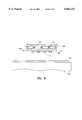
- FIG. 7shows a cutaway view of a carrier for testing fine pitch devices.
- FIG. 8is a perspective view illustrating one embodiment of the alignment template for a fine pitch device, and more specifically, a semiconductor wafer.
- FIG. 9shows an individual die on a semiconductor wafer being electrically probed.
- the present inventionsolves deficiencies of the prior art to achieve testing of a bare singulated die and other fine pitch devices by creating a carrier which is designed to hold a fine pitch device and to establish electrical continuity with the contact points of the fine pitch devices.
- These deficienciesare primarily solved by the utilization of electrically conductive elastomeric probes to contact the contact points of the fine pitch device, by way of example, the bond pads of a die, an alignment template to position the fine pitch device, and an overall configuration which allows for repetitive and labor efficient use of the carrier.
- some fine pitch devicesby way of example, a bare die, can be held in place throughout testing. This allows the bare die to be tested and certified for all required temperatures.
- FIG. 1there is shown a cutaway view of a die carrier in a socket configuration with a TEC and a heat exchanger.
- electrical contact between the circuit pads 4b of a die carrier 4 and the bond pads 2a of a bare die 2occurs through the elastomeric probes 4a.
- die carrier 4contains a plurality of circuit pads 4b which are arranged to correspond with the bond pads 2a of the bare die 2 such that the bond pads 2a of the bare die 2 line up directly over the circuit pads 4b of the die carrier 4 when the bare die 2 is properly positioned over the die carrier 4.
- the method of placing the circuit pads 4b on the surface of the die carrier 4is old and well known in the art.
- the conductive elastomeric probes 4aare permanently placed upon circuit pads 4b, wherein the elastomeric probes 4a have been designed to continuously and repetitively establish electrical continuity between it and either bond pads 2a of different die 2, or any other type of electrically conductive probe or lead including other elastomeric probes. Specifically, after the probes are placed onto the circuit pads 4b, they are cured to establish a resilient non-adhesive surface to support repetitive contacts with other conductors. It is not a requirement that every bond pad 2a on the die 2 have a corresponding circuit pad 4b on the die carrier 4. The only circuit pads 4b required on the die carrier 4 are the ones through which electrical signals are to be applied and/or measured during testing.
- the preferred embodimentincludes a pad pattern on the die carrier 4 which is a mirror image of the bond pad pattern of the bare die 2.
- the shape or size of the circuit padmay be varied so long as permanent contact may be established with the electrically conductive elastomeric probe of the carrier.
- each circuit pad 4b of the die carrier 4contains an electrically conductive elastomeric probe 4a which is permanently mounted thereon.
- Various methodscan be utilized for depositing these conductive elastomeric probes 4a on the circuit pads 4b.
- the one found to be the most satisfactory to this inventoris to have the conductive elastomeric probes 4a screened or stenciled onto the circuit pads 4b and cured through conventional methods as are known by those skilled in the art as described. For example, see U.S. Pat. No. 5,074,947 which is incorporated herein by reference for all purposes.
- the composition of the elastomeric probesis not significant so long as the elastomeric probes 4a meet certain performance criteria.
- the performance criteria for testing bare dieinclude: (1) the elastomer must be able to withstand wide ranges of temperature, the minimum sustained temperature being minus 55° Celsius and the maximum temperature being plus 125° Celsius (in the event Military certification is desired); (2) the elastomeric probes 4a must be somewhat malleable in texture; and (3) the elastomeric probes 4a must provide a low throughput resistance over a wide frequency range and must be able to freely conduct electricity as a result of being doped with a proper conductive doping agent as is known by those skilled in the art.
- the composition of acceptable elastomersinclude, but are not limited to, polyepoxides, polystyrenes, polyimides and other elastomeric polymers and epoxies.
- the preferred materialis an electrically conductive epoxy resin. Proper doping agents to impart electrical conductivity to the resins include tungsten, gold, copper and silver.
- the preferred doping agentis silver which has been used to render adhesives electrically conducting as described in U.S. Pat. No. 5,196,371 and U.S. Pat. No. 5,237,130, both being issued to Kulesza et al, incorporated herein for all purposes.
- the concept of utilizing conductive polymerscan be manifested in other similar and undeveloped compounds or with other doping agents not mentioned herein and is an intended part of the invention.
- FIG. 2shows one means for orienting; namely, an alignment template 6.
- the alignment template 6is permanently mounted onto the die carrier 4 (as is also shown in FIGS. 1, 3, 5 and 6).
- the alignment template 6contains an aperture 8 corresponding to the size and shape of the bare die 2 being tested.
- This alignment template 6is designed to receive the bare die 2 and to orient the bond pad 2a pattern of the die 2 into alignment with the corresponding electrically conductive elastomeric probes 4a of the die carrier 4.
- the alignment template 6has an outer perimeter, size and shape which is substantially the same as the outer perimeter of the die carrier 4. Furthermore, the alignment template 6 is made out of a substance whose thermal coefficient of expansion matches that of the die carrier 4 and is designed to be permanently mounted on top of it.
- the alignment template 6may be made either out of a polyimide sheet, a printed circuit board, a ceramic material or any other high temperature, high dielectric strength material.
- the corresponding die carrier 4may be made out of printed circuit board, ceramic or other high temperature, high dielectric strength materials. As is shown in FIGS. 1, 3, 5 and 6, the alignment template 6 is attached to the top surface of die carrier 4.
- the use of ceramic substrate material for fabrication of the die carrier 4 and a polyimide alignment template 6are utilized. It is not significant that the practitioner utilize a substance other than printed circuit board material for the die carrier or a polyimide sheet for the alignment template. Thus, the actual embodiment or material of an alignment template is not significant and is included herein as a part of the invention.
- guidance points 9small and firm protrusions placed to define the area in which a bare die 2 is to be placed, herein "guidance points 9", are permanently mounted onto the die carrier 4.
- the bare die 2fits within the pattern of guidance points 9 such that the bond pads 2a of bare die 2 (not shown) contact the elastomeric probes 4a of the die carrier 4 whenever the die 2 is placed within the pattern of guidance points 9. It is helpful to visualize the arrangement of these guidance points 9 as a series of fence posts which define the perimeter of the shape of the die wherein the die 2 fits exactly within this perimeter of guidance points 9.
- circuit 4illustrates a top view of this relationship between the arrangement of circuit pads 4b of a die carrier 4 and an arrangement of guidance points 9. Note that not all of the circuit pads 4b contain a conductive elastomeric probe 4a. The only requirement is that, at a minimum, the circuit pads 4b through which electrical signals must be supplied or monitored will contain elastomeric probes 4a. However, for other reasons, a practitioner can determine if it is desirable to have additional elastomeric probes. For example, requirements of structural support or engineering economy may encourage the utilization of "extra" probes 4a.
- a robotic devicei.e., a computer controlled mechanical arm, is used to pick up the die 2 from an input tray or "waffle pack" (not shown), place it onto the die carrier 4 with high precision, and to hold the bare die 2, onto the elastomeric bumps 4a of the die carrier 4 such that the die bond pads 2a maintain electrical continuity with the circuit pads 4b of the carrier 4.
- the robot arm(not shown) not only orients the die 2 such that the die bond pads 2a are in communication alignment with the circuit pads 4a of the die carrier, but also pushes or forces the die 2 at least to the point that the bond pads 2a are in firm and electrical contact with the electrically conductive elastomeric probes 4b.
- the robotic mechanismis programmed to place the die 2 repeatably and with great accuracy, thereby providing for a higher rate of handling than with manual placement. To aid in placement accuracy, optical alignment may be used with the robotic mechanism.
- the robotic mechanismalso can remove the tested die 2 from the carrier 4 and place it in the appropriate output tray or waffle pack, separating good die 2 from failures.
- the obvious advantage of this embodimentis that it is oriented for assembly line style testing with low overhead labor costs.
- the means for connecting the diethere are at least three embodiments for the means for connecting the die to a given test instrument.
- the means for connectingis standard circuit wiring which electrically connects the circuit pads 4b of the die carrier 4 to its leads 5.
- Each circuit pad 4b of the die carrier 4will be connected to at least one lead 5 of the die carrier 4.
- FIG. 1also illustrates bare die 2 being within the alignment template 6 wherein the bond pads 2a of the bare die 2 are in contact with the elastomeric probes 4a which are permanently mounted on the circuit pads 4b of the die carrier 4 which in turn are connected to the individual leads 5 through the connection lines 4c.
- the figuresshow bare die 2 with raised bond pads 2a. However, it is common to recess the bond pads 2a into the die. Thus, the malleable nature of the probes 4a assists in establishing continuity between the bond pads 2a and the probes 4a.
- the leads 5 and connection lines 4c(and connection lines lob of the carrier connector 10 as is shown in FIG. 3) used to interface the die carrier to other circuity may vary in composition and orientation and are not a significant part of this invention.
- circuit pads 4bthere may be leads 5 on the die carrier 4 which are unconnected to the circuit pads 4b.
- the exact arrangement or electrical interconnection between the circuit pads 4b and the leads 5is a function of the number of bond pads 2a of the die 2 to which electrical continuity must be established for the purposes of testing. Because such arrangements will vary widely according to the particular die 2 being testing in relation to the test requirements for that die 2, the specific arrangement cannot be specified herein. However, one skilled in the art can readily ascertain without undue experimentation what the interconnect scheme should be.
- a die carrier 4mates with a carrier connector 10.
- the circuit pads 4b of the die carrier 4are placed upon its top surface while its connection pads 4d are placed on its bottom side.
- the carrier connector's connection pads 10aare individually connected to the leads 5 of the carrier connector 10 through connection lines 10b.
- connection pads 4d of the die carrier 4 and the connection pads 10a of the carrier connector 10can be arranged in any format.
- One good arrangementis to have a row of connection pads 4d of the die carrier 4 at each end of the die carrier 4.
- the carrier connector 10contains a similar arrangement wherein the row of the carrier connector's connection pads 10a on the carrier connector 10 is designed to make electrical contact with the row of connection pads 4d of the die carrier 4.
- the arrangement of carrier connector's connection pads 10ais immaterial so long as the placement corresponds with, or is a mirror image of, the connection pads 4d of the die carrier 4.
- One advantage of this embodiment, namely the use of a carrier connector 10is that one carrier connector 10 could interface with a multitude of die carriers 4 with a matching arrangement of connection pads 4d.
- a surface mounted carrier connector 12is mounted to the surface of a burn-in board 14 (or "mother board").
- this surface mounted carrier connector 12uses an elastomeric interconnection lead 12a, as disclosed by U.S. Pat. No. 5,074,947, to establish electrical continuity between the burn-in board connection pads 14a and the bottom connection pads 4d of a die carrier 4.
- Use of this type of carrier connector for surface mount applicationsis advantageous because of lower labor cost in installing it when compared to the carrier connector 12 or any other device utilizing metal leads 5 which require soldering of individual leads 5.
- the elastomeric interconnect leads 12ahave an increased frequency bandwidth in comparison to the thin metallic leads 5a of the standard carrier connector.
- the ceramic spacer 7ais designed to be placed between the alignment template 6 and a socket lid 7 (as shown in FIG. 1) of a production socket (not shown) which houses the die carrier 4, the alignment template 6 and the bare die 2.
- the purpose of the spaceris to urge the die against the elastomeric probes 4a.
- the spacer and production socketare designed so that thermoelectric cooler (TEC) 30 (as is shown in FIG. 5) can be substituted for the spacer 7a to allow for testing at temperatures above or below ambient.
- TECthermoelectric cooler
- auxiliary cooling heat exchanger 24a thermoelectric cooler 30, a bare die 2, a die carrier 4 and surface mounted carrier connector 12, in a surface mount socket configuration
- the TEC 30is placed adjacent to and is urged into direct contact with the bare die 2.
- an auxiliary cooling heat exchanger 24is urged against the hot side of the TEC 30.
- This configurationis used whenever the die 2 must be tested at non-room temperatures, or when it is necessary to overcome internal heating of the bare die 2.
- Such a configurationwill support the range of temperatures required for all known certification procedures including military certification for the bare die 2. Specifically, military certification requires that the die be operationally certified at minus 55° Celsius as well as at plus 125° Celsius. If this configuration is used for testing discrete components or other devices, a practitioner should insure that its TEC is capable of supporting the rigid temperature range.
- One methodincludes placing the die 2 and a die carrier 4 within the heating/cooling chamber of a temperature forcing unit (not shown) of some sort.
- Heating and cooling chambers(not shown), however, take significantly longer than a TEC/auxiliary cooler to raise or lower the die temperature.
- the use of such a systemgreatly reduces overall test time and therefore, cost of performing the test.
- the use of a convective temperature forcing devicesuch as a conventional oven (not shown) can take several times as long for the die 2 to reach the desired temperature.
- the method of using the thermoelectric cooler/heateris well known in the art and can be readily determined from the vendors of such devices.
- thermoelectric cooler shown in FIG. 5includes vacuum line 26 for holding the die.
- An auxiliary cooling systemmay be used, containing an inlet line 24a, and an outlet line 24b for circulating cooled water through the auxiliary cooling system 24 which in turn further cools the TEC hot side.
- the inventorhas found that it may be advantageous to purge the die with nitrogen gas to prevent frost build-up.
- the clamp 20supports "burn-in" testing in a conventional oven.
- Clamp 20, which is attached to the die carrier 4will hold the die 2 in place such that the bond pads 2a of the die 2 maintain electrical continuity with the electrically conductive elastomeric probes 4a which are permanently attached to the circuit pads 4b of the die carrier 4.
- the bolt 20bwill rotate in a downward manner through clamp plate 20a thereby forcing clamp press 20c in a downward manner to urge the bare die 2 against the electrically conductive elastomeric bumps 4a.
- a production socket(not shown) could accomplish the same task if ceramic spacer 7a is placed within the socket. Because the die carrier 4 is electrically connected with the carrier connector 10, the carrier connector 10 may be plugged into a burn-in board 14 for the continuous "burn-in" testing process.
- the burn-in board 14, in turn,is connected to various pieces of test equipment through standard wiring in a manner well understood by those skilled in the art.
- die 2have been "burned in” after being packaged. Because electrical contacts with the external leads of the package can be reliably maintained, there is little reason to be concerned that electrical continuity will be lost during the burn-in process of a packaged die. However, since this single bare die 2 is not permanently packaged, continuous electrical contact during burn-in can no longer be assumed. Therefore, the method of burn-in for the bare die 2 may include continuous or periodic electronic data sampling to insure that electrical continuity is maintained. Once a die 2 successfully completes "burn-in” and post burn-in electrical tests, then that die 2 may be labeled or certified as a "known good die".
- burn-inis a term of art which varies significantly within the electronics industry, the inventor's burn-in process, as it relates to bare semiconductor die, is as follows: Initially, the die 2 is placed within a production socket (not shown) or within a die clamp 20 as is shown in FIG. 6 for pre-burn-in electrical testing. Once the die 2 is within a production socket (not shown) or a die clamp 20, it is connected to a piece of electrical test equipment for comprehensive functional testing of the die. In other words, the die is tested to the point that a practitioner can determine, in all probability, that each of the die's capabilities or functions works properly. Alternatively, the die 2 could be placed within a die carrier 4 that is thermally connected to a TEC 30, as is shown in FIG.
- An advantage to performing a pre-burn-in test at a raised (or lowered) temperatureis that a defective die is more likely to fail. Obviously, money is saved by identifying defective die as quickly as possible.
- the practitionermay utilize any type of production socket so long as it can house a die carrier 4 and an alignment template 6.
- the production socketmust also be able to house a spacer 7a sized to define the same geometric volume of space as defined by a thermoelectric cooler 30.
- a spacer 7asized to define the same geometric volume of space as defined by a thermoelectric cooler 30.
- the die 2 and die carrier 4are connected to a burn-in board 14 and then placed into an oven (not shown) and kept at a raised temperature for a length of time according to test or certification specifications.
- the inventor's preferred pre-burn-in methodtests the die at elevated temperatures. However, other test procedures may require lowered temperatures.
- One example of a burn-in procedurewould be to operate the die 2 through the burn-in board 14 within an oven at 125° Celsius for a minimum of 24 hours. For some applications, the die 2 may be kept in the oven for as many as 168 hours (or longer for other devices). The time that the die 2 is kept in the oven, as well as the oven temperature, is determined by the certification standard being followed for the particular die.
- the die 2While the die 2 is within the oven, the die is "exercised” or operated at a level less than or equal to its full functional capability. Further, the operation may be monitored repetitively to insure the die 2 has successfully operated and that electrical continuity has been maintained during the burn-in process. Because the die 2 is housed in temporary packaging and continuous electrical continuity cannot be assumed, a given output signal or contents of a data register may be repetitively checked to verify that new or fresh signals or data are being introduced into the die and that the die 2 is satisfactorily processing the signals or data. Finally, it should be noted that these burn-in procedures could be carried out with a thermoelectric cooler instead of in an oven. As a practical matter, however, burn-in testing in an oven allows for a greater number of die to be "burned in” simultaneously and is therefore preferred.
- Post burn-in electrical testingincludes electrically testing the die 2 at 25° Celsius (ambient or room temperature), then at a high temperature, up to (+) 125° Celsius, and finally at a low temperature, which can be as low as (-) 55° Celsius.
- the desired temperatures and the length of time for the comprehensive electrical testingare a function of the certification standard being applied to the specific die 2.
- Use of the thermoelectric cooler 30 for the post burn-in testsgreatly expedites the test procedures because the thermoelectric cooler, in conjunction with an auxiliary cooling heat exchanger 24, greatly reduces the time necessary to raise and lower the temperature of the bare die 2, within approximately one minute. Further, this series of tests at the various temperatures can be performed without having to physically move or reconnect the die to any other equipment.
- each of the bond pads 2a of the bare die 2may be cleaned prior to the bare die 2 being placed onto the conductive elastomeric probes 4a.
- An oxide buildup on the bond pads 2amay cause high resistance and prevent probe 4a from making electrical contact with pad 2a.
- the oxide buildup on the bond pads 2amay be removed chemically, ultrasonically, physically through the use of some sort of scrubbing device, or through some other method such as ion etching. It should be noted that the die 2 must be handled properly during the entire process, including the cleaning process, to prevent it from being damaged by spurious electrostatic charges.
- the test socket 100is adapted for testing fine pitch devices including semiconductor wafers. Similar to the bare die test socket of FIGS. 1-6, the test socket 100 is adapted to receive the fine pitch device 30, which fine pitch device 30 is comprised of a plurality of contact points 32, which contact points 32 are contacted by the conductive elastomeric probes 34 of the test socket 100. As with the test socket of FIGS. 1-6 for the bare die 2, the malleable and electrically conductive elastomeric probes 34 are printed by conventional means (e.g., as practiced by Epoxy Technology of Boston, Mass.) onto circuit pads 36 in one embodiment of the invention, which circuit pads 36 are a part of the carrier 38. Moreover, as may be seen for the embodiment of FIG. 7, the carrier 38 further comprises connection pads 40 at the bottom of the carrier 38 wherein the circuit pads 36 are connected to the connection pads 40 by the traces 42.
- the carrier 38further comprises connection pads 40 at the bottom of the carrier 38 wherein the circuit pads 36 are connected to the connection pads 40 by the traces
- the test socket 100 of FIG. 7also comprises a carrier connector 44, which carrier connector 44 is comprised of connector leads 46 which are adapted for electrically contacting the connection pads 40 of the carrier 38.
- the carrier connector 44comprises traces 48 which connect the connector leads 46 to external circuitry (not shown).
- the test socket 100is mounted directly onto a high temperature printed circuit board 90.
- the test socket 100is comprised of a plurality of the walls 110 which form an aperture 120 through which the fine pitch device 30 is placed to contact the elastomeric probes 34 of carrier 38.
- the fine pitch device 30is urged in a downward direction as indicated by the arrows 60 through an alignment template 70 wherein proper alignment exists between the contact points 32 and the carrier 38. More specifically, the contact points 32 must align with the probes 34 whenever fine pitch device 30 is interposed through an alignment template 70.
- an alignment template 70may be constructed of different materials and machined in different ways, an alignment template 70 should be carefully designed and fabricated to obtain and maintain proper alignment during test and burn-in test. More specifically, because it is known that the various materials utilized for fabricating the test socket and the alignment template will expand or contract during burn-in, it is important to fabricate an alignment template having a thermal co-efficient of expansion which is similar to that of the test socket and preferably out of materials having good thermal stability. Otherwise, in a worst case scenario, the semiconductor wafer could become misaligned relative to the probes of the test socket 100 during the testing process.
- both the test socket 100 as well as the alignment templateare fabricated with a polyetherimide such as Ultem® 1000 polyetherimides.
- alignment template 70is laser machined to insure precision.
- a laser machined alignment template 70can be used to align the semiconductor wafer 30 properly, even though there may be 5,000 or 10,000 bond pads 32 on the semiconductor wafer 30, because the overall dimensions and size of the semiconductor wafers 30 vary little, given current semiconductor wafer processing technologies.
- the test socket 100 and alignment template 70are both made out of Ultem® polyethermide.
- the socket 100is mounted on a high temperature printed circuit board 90 as is shown in FIG. 7.
- cover 80which may be used to urge the fine pitch device 30 in a downward direction 60 and to hold the fine pitch device 30 in place during testing or burn-in test.
- cover 80is replaced with a thermoelectric cooler similar to that thermoelectric cooler 30 shown in FIG. 5 wherein such TEC is sized and adapted for being urged against the semiconductor wafer 30, instead of the bare die 2.
- FIG. 7contains bond pads 32, circuit pads 36, elastomeric probes 34 and connection pads 40 which are drawn out of scale for the purposes of illustration.
- some fine pitch devicesnamely, semiconductor wafers, may have 5,000 such bond pads 32.
- the relative size of probes 34, bond pads 32 and circuit pads 36is very small in comparison to the test socket.
- circuit padsby way of example, the circuit pads 36 of carrier 38 of FIG. 7, may be modified in size or shape so long as permanent electrical contact is made with elastomeric probes 34 (of FIG. 7).
- FIG. 8there is shown a perspective view of an alignment template 70 which comprises aperture 72, which is adapted to mate with the fine pitch device 30, which, for this example, is a semiconductor wafer, when the fine pitch device 30 is urged in a downward direction 60 through aperture 72.
- the fine pitch device 30also includes a plurality of optical marks 74 which are used to optically align semiconductor wafer 30 with an optical device (not shown).
- FIG. 8there is shown another embodiment of the invention wherein an alignment template 70 is used to place the fine pitch device 30 into approximate alignment while a standard optical device for aligning semiconductor devices is used to locate predesignated marks 74 on the fine pitch device 30 and to adjust the alignment of the fine pitch device 30.
- Optical devices for aligning the fine pitch device 30 or the bare die 2 (of FIG. 1) and the method of using such devicesare known and can be readily appreciated by those skilled in the art.
- the fine pitch device 30is held in place by a vacuum instead of an alignment template 70. The position of the fine pitch device is adjusted by adjusting the position of the vacuum device.
- a wafer probe testeris shown.
- Such a testerwell known to those skilled in the art and widely available from many sources, comprises a platform 130 and probe card 150.
- a die carrier 4previously described, is mounted to the probe card 150 with standard mounting brackets 160.
- a semiconductor wafer 30is disposed between the platform 130 and probe card 150 and held to the platform 130 by a vacuum in a conventional, well known manner. Electrical contact to the die carrier from the probe card 150 is made by pins 140 contacting connection pads 4d on the die carrier 4. The connection pads 4d are electrically connected to circuit pads 4b. Elastomeric probes 4a are permanently mounted on the circuit pads 4b. The wafer probe machine places the elastomeric probes against the pads of the die.
- the elastomeric probes 4aare in a mirror image ofthe pads on the die.
- the methods for aligning the pads of the dieare well known to those skilled in the art. One method requires manual adjustment while looking through a hole in the die carrier. Another method employs the use of split vision optics. Once electrical testing is performed on a die, the wafer probe machine moves the probe card 150 with the die carrier 4 attached to the next die.
- the prior art methods of producing integrated circuitsinclude using a wafer probe to perform simple DC and some AC testing to preliminarily eliminate 80% of all bad die 76 on semiconductor wafer 30, then to saw the wafer 30 and package the bare die 2 to create an integrated circuit prior to performing certification tests.
- the process of certifying an integrated circuitincludes performing 100% pre-burn-in testing, then burn-in and then 100% post burn-in testing. At such point, integrated circuits having failed along the way are rejected and the rest are processed for sale or for use.
- a different methodmay be used with respect to producing integrated circuits and other semiconductor devices formed on a semiconductor wafer, one that significantly reduces the number of steps involved in testing all of the individual integrated circuits produced from a semiconductor wafer.
- fine pitch device 30When fine pitch device 30 is diced post burn-in to separate die 76, the failed die 76, as indicated by the map, are separated and discarded. After failed die 76 are separated from fine pitch device 30, the remaining bare die 2 undergo complete testing to verify complete and proper performance of bare die 2. For this stage of the test process, the test sockets of FIGS. 1-6 described above may be utilized. Bare die 2 which pass this stage of the test process are known good die which may be either packaged individually as an integrated circuit or as a part of a multi-chip module. Alternatively, after the wafer level burn-in and dicing, the remaining bare die 2 may also be packaged prior to being fully tested.
- the carrier and inventive methodsmay be made according to the type of fine pitch device being tested.
- the fine pitch device 30 of FIG. 7is a printed circuit board, then the requirement for burn-in-test may be modified or even eliminated.
- the disclosureis directed to describing a test socket for testing fine pitch devices and is not limited merely to bare die and semiconductor wafers, but applies to any fine pitch device. Accordingly, one skilled in the art may readily appreciate changes in the physical dimensions of a carrier, and perhaps methods (as determined by test goals) to perform tests upon the specific fine pitch device.
- Such changesmay be necessary to test fine pitch devices such as bare die, unpackaged semiconductor devices such as semiconductor wafers, as well as packaged semiconductor devices and modern circuitry for testing or carrying semiconductor devices including probe cards, bare printed circuit boards, populated circuit boards, ball grid arrays, ceramic ball grid arrays and chip-scale packages.
Landscapes
- Physics & Mathematics (AREA)
- General Physics & Mathematics (AREA)
- Engineering & Computer Science (AREA)
- Computer Hardware Design (AREA)
- Microelectronics & Electronic Packaging (AREA)
- Geometry (AREA)
- Testing Of Individual Semiconductor Devices (AREA)
Abstract
Description
Claims (24)
Priority Applications (2)
| Application Number | Priority Date | Filing Date | Title |
|---|---|---|---|
| US08/705,886US6064217A (en) | 1993-12-23 | 1996-08-28 | Fine pitch contact device employing a compliant conductive polymer bump |
| US09/193,830US20020011859A1 (en) | 1993-12-23 | 1998-11-17 | Method for forming conductive bumps for the purpose of contrructing a fine pitch test device |
Applications Claiming Priority (4)
| Application Number | Priority Date | Filing Date | Title |
|---|---|---|---|
| US17258093A | 1993-12-23 | 1993-12-23 | |
| US08/427,974US5475317A (en) | 1993-12-23 | 1995-04-21 | Singulated bare die tester and method of performing forced temperature electrical tests and burn-in |
| US57015995A | 1995-12-11 | 1995-12-11 | |
| US08/705,886US6064217A (en) | 1993-12-23 | 1996-08-28 | Fine pitch contact device employing a compliant conductive polymer bump |
Related Parent Applications (1)
| Application Number | Title | Priority Date | Filing Date |
|---|---|---|---|
| US57015995AContinuation-In-Part | 1993-12-23 | 1995-12-11 |
Related Child Applications (1)
| Application Number | Title | Priority Date | Filing Date |
|---|---|---|---|
| US09/193,830Continuation-In-PartUS20020011859A1 (en) | 1993-12-23 | 1998-11-17 | Method for forming conductive bumps for the purpose of contrructing a fine pitch test device |
Publications (1)
| Publication Number | Publication Date |
|---|---|
| US6064217Atrue US6064217A (en) | 2000-05-16 |
Family
ID=27390164
Family Applications (1)
| Application Number | Title | Priority Date | Filing Date |
|---|---|---|---|
| US08/705,886Expired - Fee RelatedUS6064217A (en) | 1993-12-23 | 1996-08-28 | Fine pitch contact device employing a compliant conductive polymer bump |
Country Status (1)
| Country | Link |
|---|---|
| US (1) | US6064217A (en) |
Cited By (95)
| Publication number | Priority date | Publication date | Assignee | Title |
|---|---|---|---|---|
| US20010052642A1 (en)* | 2000-06-16 | 2001-12-20 | Wood Alan G. | Semiconductor device package and method |
| US6384613B1 (en)* | 1998-02-16 | 2002-05-07 | Amic Technology, Inc. | Wafer burn-in testing method |
| US6392161B1 (en)* | 1999-02-10 | 2002-05-21 | Sony Corporation | Mounting substrate |
| US6410415B1 (en)* | 1999-03-23 | 2002-06-25 | Polymer Flip Chip Corporation | Flip chip mounting technique |
| US6414501B2 (en) | 1998-10-01 | 2002-07-02 | Amst Co., Ltd. | Micro cantilever style contact pin structure for wafer probing |
| US6417027B1 (en) | 1999-06-10 | 2002-07-09 | Micron Technology, Inc. | High density stackable and flexible substrate-based devices and systems and methods of fabricating |
| US6429835B1 (en) | 1995-01-24 | 2002-08-06 | Micron Technologies, Inc. | Method and apparatus for testing emissive cathodes |
| US6433564B1 (en)* | 1999-06-14 | 2002-08-13 | St Assemby Test Services Pte. Ltd | BGA device positioner kit |
| US6462568B1 (en) | 2000-08-31 | 2002-10-08 | Micron Technology, Inc. | Conductive polymer contact system and test method for semiconductor components |
| US6472892B2 (en)* | 1999-12-21 | 2002-10-29 | Infineon Technologies Ag | Configuration for testing chips using a printed circuit board |
| US6529026B1 (en)* | 1997-08-22 | 2003-03-04 | Micron Technology, Inc. | Method for fabricating an interconnect for making temporary electrical connections to semiconductor components |
| US6535006B2 (en)* | 2000-12-22 | 2003-03-18 | Intel Corporation | Test socket and system |
| US6552555B1 (en)* | 1998-11-19 | 2003-04-22 | Custom One Design, Inc. | Integrated circuit testing apparatus |
| US6560108B2 (en)* | 2000-02-16 | 2003-05-06 | Hughes Electronics Corporation | Chip scale packaging on CTE matched printed wiring boards |
| US6559818B1 (en) | 1995-01-24 | 2003-05-06 | Micron Technology, Inc. | Method of testing addressable emissive cathodes |
| US6566245B2 (en) | 1998-01-17 | 2003-05-20 | Acuid Corporation (Guernsey) Limited | Method of manufacturing probe unit and probe unit manufactured using this method |
| US6575764B1 (en)* | 1998-05-22 | 2003-06-10 | Reipur Technology A/S | Means for providing electrical contact |
| US6598290B2 (en) | 1998-01-20 | 2003-07-29 | Micron Technology, Inc. | Method of making a spring element for use in an apparatus for attaching to a semiconductor |
| US6601753B2 (en)* | 2001-05-17 | 2003-08-05 | Visteon Global Technologies, Inc. | Void-free die attachment method with low melting metal |
| US20030202768A1 (en)* | 2001-05-25 | 2003-10-30 | Steven Nasiri | High density optical fiber array |
| US20030232524A1 (en)* | 2002-06-18 | 2003-12-18 | Burdick Robert C. | Low current minimal alignment compression contact system |
| US6703640B1 (en)* | 1998-01-20 | 2004-03-09 | Micron Technology, Inc. | Spring element for use in an apparatus for attaching to a semiconductor and a method of attaching |
| US20040061515A1 (en)* | 2002-09-30 | 2004-04-01 | Keeny Chang | Flip chip test structure |
| WO2004038433A1 (en) | 2002-10-28 | 2004-05-06 | Jsr Corporation | Sheet-form connector and production method and application therefor |
| US20040189333A1 (en)* | 2003-01-10 | 2004-09-30 | Stephan Dobritz | Carrier for receiving and electrically contacting individually separated dies |
| KR100508088B1 (en)* | 2003-02-28 | 2005-08-17 | 삼성전자주식회사 | Apparatus and method for testing chip scaled package |
| US20050202597A1 (en)* | 2004-03-12 | 2005-09-15 | Noriyuki Takahashi | Manufacturing method of a tray, a socket for inspection, and a semiconductor device |
| US20050260868A1 (en)* | 2004-05-18 | 2005-11-24 | Jong-Joo Lee | Test apparatus having intermediate connection board for package |
| US20060009055A1 (en)* | 2004-07-09 | 2006-01-12 | Che-Yu Li | Interconnection device and system |
| US20060008226A1 (en)* | 2001-05-04 | 2006-01-12 | Cascade Microtech, Inc. | Fiber optic wafer probe |
| US20060028226A1 (en)* | 2004-07-21 | 2006-02-09 | Kreager Douglas P | Methods and apparatus for testing circuit boards |
| US7052290B1 (en)* | 2005-08-10 | 2006-05-30 | Sony Ericsson Mobile Communications Ab | Low profile connector for electronic interface modules |
| US7161363B2 (en) | 2002-05-23 | 2007-01-09 | Cascade Microtech, Inc. | Probe for testing a device under test |
| US20070094867A1 (en)* | 2002-01-30 | 2007-05-03 | Texas Instruments Incorporated | Bond Surface Conditioning System for Improved Bondability |
| US7233160B2 (en) | 2000-12-04 | 2007-06-19 | Cascade Microtech, Inc. | Wafer probe |
| US7271603B2 (en) | 2003-05-23 | 2007-09-18 | Cascade Microtech, Inc. | Shielded probe for testing a device under test |
| US7285969B2 (en) | 2002-11-13 | 2007-10-23 | Cascade Microtech, Inc. | Probe for combined signals |
| US20070252288A1 (en)* | 2003-11-25 | 2007-11-01 | Farooq Mukta G | Semiconductor module and method for forming the same |
| US20070268031A1 (en)* | 2006-05-18 | 2007-11-22 | Centipede Systems, Inc. | Wafer Probe Interconnect System |
| US7321233B2 (en) | 1995-04-14 | 2008-01-22 | Cascade Microtech, Inc. | System for evaluating probing networks |
| US20080020600A1 (en)* | 2005-09-08 | 2008-01-24 | International Business Machines Corporation | Land grid array (lga) interposer utilizing metal-on-elastomer hemi-torus and other multiple points of contact geometries |
| US7330041B2 (en) | 2004-06-14 | 2008-02-12 | Cascade Microtech, Inc. | Localizing a temperature of a device for testing |
| US7348787B2 (en) | 1992-06-11 | 2008-03-25 | Cascade Microtech, Inc. | Wafer probe station having environment control enclosure |
| US7352168B2 (en) | 2000-09-05 | 2008-04-01 | Cascade Microtech, Inc. | Chuck for holding a device under test |
| US7355420B2 (en) | 2001-08-21 | 2008-04-08 | Cascade Microtech, Inc. | Membrane probing system |
| US7362115B2 (en) | 2003-12-24 | 2008-04-22 | Cascade Microtech, Inc. | Chuck with integrated wafer support |
| US7368925B2 (en) | 2002-01-25 | 2008-05-06 | Cascade Microtech, Inc. | Probe station with two platens |
| US7368927B2 (en) | 2004-07-07 | 2008-05-06 | Cascade Microtech, Inc. | Probe head having a membrane suspended probe |
| US7403028B2 (en) | 2006-06-12 | 2008-07-22 | Cascade Microtech, Inc. | Test structure and probe for differential signals |
| US7403025B2 (en) | 2000-02-25 | 2008-07-22 | Cascade Microtech, Inc. | Membrane probing system |
| US7420381B2 (en) | 2004-09-13 | 2008-09-02 | Cascade Microtech, Inc. | Double sided probing structures |
| US7427868B2 (en) | 2003-12-24 | 2008-09-23 | Cascade Microtech, Inc. | Active wafer probe |
| US7436170B2 (en) | 1997-06-06 | 2008-10-14 | Cascade Microtech, Inc. | Probe station having multiple enclosures |
| US7443186B2 (en) | 2006-06-12 | 2008-10-28 | Cascade Microtech, Inc. | On-wafer test structures for differential signals |
| US7449899B2 (en) | 2005-06-08 | 2008-11-11 | Cascade Microtech, Inc. | Probe for high frequency signals |
| US7468609B2 (en) | 2003-05-06 | 2008-12-23 | Cascade Microtech, Inc. | Switched suspended conductor and connection |
| US20080318348A1 (en)* | 2007-06-25 | 2008-12-25 | Spansion Llc | Method of constructing a stacked-die semiconductor structure |
| US7492147B2 (en) | 1992-06-11 | 2009-02-17 | Cascade Microtech, Inc. | Wafer probe station having a skirting component |
| US7492172B2 (en) | 2003-05-23 | 2009-02-17 | Cascade Microtech, Inc. | Chuck for holding a device under test |
| US7498828B2 (en) | 2002-11-25 | 2009-03-03 | Cascade Microtech, Inc. | Probe station with low inductance path |
| US20090068858A1 (en)* | 2007-08-17 | 2009-03-12 | Centipede Systems, Inc. | Miniature electrical ball and tube socket assembly with self-capturing multiple-contact-point coupling |
| US7504842B2 (en) | 1997-05-28 | 2009-03-17 | Cascade Microtech, Inc. | Probe holder for testing of a test device |
| US7504823B2 (en) | 2004-06-07 | 2009-03-17 | Cascade Microtech, Inc. | Thermal optical chuck |
| US20090102498A1 (en)* | 2007-10-19 | 2009-04-23 | Teradyne, Inc. | Laser Targeting Mechanism |
| US7535247B2 (en) | 2005-01-31 | 2009-05-19 | Cascade Microtech, Inc. | Interface for testing semiconductors |
| US7533462B2 (en) | 1999-06-04 | 2009-05-19 | Cascade Microtech, Inc. | Method of constructing a membrane probe |
| US7541821B2 (en) | 1996-08-08 | 2009-06-02 | Cascade Microtech, Inc. | Membrane probing system with local contact scrub |
| US7550984B2 (en) | 2002-11-08 | 2009-06-23 | Cascade Microtech, Inc. | Probe station with low noise characteristics |
| US7554322B2 (en) | 2000-09-05 | 2009-06-30 | Cascade Microtech, Inc. | Probe station |
| US20090251698A1 (en)* | 2008-04-02 | 2009-10-08 | Claudius Feger | Method and system for collecting alignment data from coated chips or wafers |
| US7609077B2 (en) | 2006-06-09 | 2009-10-27 | Cascade Microtech, Inc. | Differential signal probe with integral balun |
| US7616017B2 (en) | 1999-06-30 | 2009-11-10 | Cascade Microtech, Inc. | Probe station thermal chuck with shielding for capacitive current |
| US7619419B2 (en) | 2005-06-13 | 2009-11-17 | Cascade Microtech, Inc. | Wideband active-passive differential signal probe |
| US7639003B2 (en) | 2002-12-13 | 2009-12-29 | Cascade Microtech, Inc. | Guarded tub enclosure |
| US7656172B2 (en) | 2005-01-31 | 2010-02-02 | Cascade Microtech, Inc. | System for testing semiconductors |
| US20100045322A1 (en)* | 2008-08-19 | 2010-02-25 | Centipede Systems, Inc. | Probe Head Apparatus for Testing Semiconductors |
| US7681312B2 (en) | 1998-07-14 | 2010-03-23 | Cascade Microtech, Inc. | Membrane probing system |
| US7723999B2 (en) | 2006-06-12 | 2010-05-25 | Cascade Microtech, Inc. | Calibration structures for differential signal probing |
| US7764072B2 (en) | 2006-06-12 | 2010-07-27 | Cascade Microtech, Inc. | Differential signal probing system |
| US20100315112A1 (en)* | 2009-06-08 | 2010-12-16 | Texas Instruments Incorporated | Socket adapter for testing singulated ics with wafer level probe card |
| US7876114B2 (en) | 2007-08-08 | 2011-01-25 | Cascade Microtech, Inc. | Differential waveguide probe |
| US7888957B2 (en) | 2008-10-06 | 2011-02-15 | Cascade Microtech, Inc. | Probing apparatus with impedance optimized interface |
| US20110156734A1 (en)* | 2009-12-31 | 2011-06-30 | Formfactor, Inc. | Test systems and methods for testing electronic devices |
| US20110223780A1 (en)* | 2010-03-15 | 2011-09-15 | Russell James V | Electrical connector for connecting an adaptor board or electrical component to a main printed circuit board |
| US8069491B2 (en) | 2003-10-22 | 2011-11-29 | Cascade Microtech, Inc. | Probe testing structure |
| US20120187972A1 (en)* | 2011-01-24 | 2012-07-26 | Chunghwa Precision Test Tech. Co., Ltd. | Wafer level testing structure |
| US20120235699A1 (en)* | 2009-10-19 | 2012-09-20 | Advantest Corporation | Test carrier |
| US8319503B2 (en) | 2008-11-24 | 2012-11-27 | Cascade Microtech, Inc. | Test apparatus for measuring a characteristic of a device under test |
| US20130052839A1 (en)* | 2011-08-30 | 2013-02-28 | Denso Corporation | Detachable connection structure |
| US8410806B2 (en) | 2008-11-21 | 2013-04-02 | Cascade Microtech, Inc. | Replaceable coupon for a probing apparatus |
| US9979150B2 (en) | 2015-12-04 | 2018-05-22 | Samsung Electronics Co., Ltd. | Socket pin and semiconductor package test system |
| US10424525B2 (en) | 2017-05-23 | 2019-09-24 | Stmicroelectronics S.R.L. | Method of manufacturing semiconductor devices |
| US10879143B2 (en) | 2017-05-23 | 2020-12-29 | Stmicroelectronics S.R.L. | Method of manufacturing semiconductor devices, corresponding device and circuit |
| US20230400478A1 (en)* | 2022-06-10 | 2023-12-14 | Chroma Ate Inc. | Liquid cooling system, liquid cooling method and electronic device-testing apparatus having the system |
| US20240103069A1 (en)* | 2022-09-22 | 2024-03-28 | Renesas Electronics Corporation | Method of testing semiconductor device and method of manufacturing semiconductor device |
Citations (28)
| Publication number | Priority date | Publication date | Assignee | Title |
|---|---|---|---|---|
| US3648002A (en)* | 1970-05-04 | 1972-03-07 | Essex International Inc | Current control apparatus and methods of manufacture |
| US3832632A (en)* | 1971-11-22 | 1974-08-27 | F Ardezzone | Multi-point probe head assembly |
| US3971610A (en)* | 1974-05-10 | 1976-07-27 | Technical Wire Products, Inc. | Conductive elastomeric contacts and connectors |
| US4288841A (en)* | 1979-09-20 | 1981-09-08 | Bell Telephone Laboratories, Incorporated | Double cavity semiconductor chip carrier |
| US4329642A (en)* | 1979-03-09 | 1982-05-11 | Siliconix, Incorporated | Carrier and test socket for leadless integrated circuit |
| US4340860A (en)* | 1980-05-19 | 1982-07-20 | Trigon | Integrated circuit carrier package test probe |
| US4437718A (en)* | 1981-12-17 | 1984-03-20 | Motorola Inc. | Non-hermetically sealed stackable chip carrier package |
| US4554505A (en)* | 1983-06-10 | 1985-11-19 | Rockwell International Corporation | Test socket for a leadless chip carrier |
| US4739257A (en)* | 1985-06-06 | 1988-04-19 | Automated Electronic Technology, Inc. | Testsite system |
| US4899107A (en)* | 1988-09-30 | 1990-02-06 | Micron Technology, Inc. | Discrete die burn-in for nonpackaged die |
| US4956605A (en)* | 1989-07-18 | 1990-09-11 | International Business Machines Corporation | Tab mounted chip burn-in apparatus |
| US5006792A (en)* | 1989-03-30 | 1991-04-09 | Texas Instruments Incorporated | Flip-chip test socket adaptor and method |
| US5006796A (en)* | 1987-10-28 | 1991-04-09 | Irish Transformers Limited | Temperature control instrument for electronic components under test |
| US5014161A (en)* | 1985-07-22 | 1991-05-07 | Digital Equipment Corporation | System for detachably mounting semiconductors on conductor substrate |
| US5061192A (en)* | 1990-12-17 | 1991-10-29 | International Business Machines Corporation | High density connector |
| US5123850A (en)* | 1990-04-06 | 1992-06-23 | Texas Instruments Incorporated | Non-destructive burn-in test socket for integrated circuit die |
| US5173451A (en)* | 1991-06-04 | 1992-12-22 | Micron Technology, Inc. | Soft bond for semiconductor dies |
| US5207585A (en)* | 1990-10-31 | 1993-05-04 | International Business Machines Corporation | Thin interface pellicle for dense arrays of electrical interconnects |
| US5248262A (en)* | 1992-06-19 | 1993-09-28 | International Business Machines Corporation | High density connector |
| US5302891A (en)* | 1991-06-04 | 1994-04-12 | Micron Technology, Inc. | Discrete die burn-in for non-packaged die |
| US5329423A (en)* | 1993-04-13 | 1994-07-12 | Scholz Kenneth D | Compressive bump-and-socket interconnection scheme for integrated circuits |
| US5358417A (en)* | 1993-08-27 | 1994-10-25 | The Whitaker Corporation | Surface mountable electrical connector |
| US5453701A (en)* | 1992-12-23 | 1995-09-26 | Honeywell Inc. | Bare die test and burn-in device |
| US5475315A (en)* | 1991-09-20 | 1995-12-12 | Audio Precision, Inc. | Method and apparatus for fast response and distortion measurement |
| US5489854A (en)* | 1993-04-01 | 1996-02-06 | Analog Devices, Inc. | IC chip test socket with double-ended spring biased contacts |
| US5493237A (en)* | 1994-05-27 | 1996-02-20 | The Whitaker Corporation | Integrated circuit chip testing apparatus |
| US5633596A (en)* | 1994-01-11 | 1997-05-27 | Key Solutions Ltd. | Fixtureless automatic test equipment and a method for registration for use therewith |
| US5656945A (en)* | 1993-05-12 | 1997-08-12 | Tribotech | Apparatus for testing a nonpackaged die |
- 1996
- 1996-08-28USUS08/705,886patent/US6064217A/ennot_activeExpired - Fee Related
Patent Citations (28)
| Publication number | Priority date | Publication date | Assignee | Title |
|---|---|---|---|---|
| US3648002A (en)* | 1970-05-04 | 1972-03-07 | Essex International Inc | Current control apparatus and methods of manufacture |
| US3832632A (en)* | 1971-11-22 | 1974-08-27 | F Ardezzone | Multi-point probe head assembly |
| US3971610A (en)* | 1974-05-10 | 1976-07-27 | Technical Wire Products, Inc. | Conductive elastomeric contacts and connectors |
| US4329642A (en)* | 1979-03-09 | 1982-05-11 | Siliconix, Incorporated | Carrier and test socket for leadless integrated circuit |
| US4288841A (en)* | 1979-09-20 | 1981-09-08 | Bell Telephone Laboratories, Incorporated | Double cavity semiconductor chip carrier |
| US4340860A (en)* | 1980-05-19 | 1982-07-20 | Trigon | Integrated circuit carrier package test probe |
| US4437718A (en)* | 1981-12-17 | 1984-03-20 | Motorola Inc. | Non-hermetically sealed stackable chip carrier package |
| US4554505A (en)* | 1983-06-10 | 1985-11-19 | Rockwell International Corporation | Test socket for a leadless chip carrier |
| US4739257A (en)* | 1985-06-06 | 1988-04-19 | Automated Electronic Technology, Inc. | Testsite system |
| US5014161A (en)* | 1985-07-22 | 1991-05-07 | Digital Equipment Corporation | System for detachably mounting semiconductors on conductor substrate |
| US5006796A (en)* | 1987-10-28 | 1991-04-09 | Irish Transformers Limited | Temperature control instrument for electronic components under test |
| US4899107A (en)* | 1988-09-30 | 1990-02-06 | Micron Technology, Inc. | Discrete die burn-in for nonpackaged die |
| US5006792A (en)* | 1989-03-30 | 1991-04-09 | Texas Instruments Incorporated | Flip-chip test socket adaptor and method |
| US4956605A (en)* | 1989-07-18 | 1990-09-11 | International Business Machines Corporation | Tab mounted chip burn-in apparatus |
| US5123850A (en)* | 1990-04-06 | 1992-06-23 | Texas Instruments Incorporated | Non-destructive burn-in test socket for integrated circuit die |
| US5207585A (en)* | 1990-10-31 | 1993-05-04 | International Business Machines Corporation | Thin interface pellicle for dense arrays of electrical interconnects |
| US5061192A (en)* | 1990-12-17 | 1991-10-29 | International Business Machines Corporation | High density connector |
| US5173451A (en)* | 1991-06-04 | 1992-12-22 | Micron Technology, Inc. | Soft bond for semiconductor dies |
| US5302891A (en)* | 1991-06-04 | 1994-04-12 | Micron Technology, Inc. | Discrete die burn-in for non-packaged die |
| US5475315A (en)* | 1991-09-20 | 1995-12-12 | Audio Precision, Inc. | Method and apparatus for fast response and distortion measurement |
| US5248262A (en)* | 1992-06-19 | 1993-09-28 | International Business Machines Corporation | High density connector |
| US5453701A (en)* | 1992-12-23 | 1995-09-26 | Honeywell Inc. | Bare die test and burn-in device |
| US5489854A (en)* | 1993-04-01 | 1996-02-06 | Analog Devices, Inc. | IC chip test socket with double-ended spring biased contacts |
| US5329423A (en)* | 1993-04-13 | 1994-07-12 | Scholz Kenneth D | Compressive bump-and-socket interconnection scheme for integrated circuits |
| US5656945A (en)* | 1993-05-12 | 1997-08-12 | Tribotech | Apparatus for testing a nonpackaged die |
| US5358417A (en)* | 1993-08-27 | 1994-10-25 | The Whitaker Corporation | Surface mountable electrical connector |
| US5633596A (en)* | 1994-01-11 | 1997-05-27 | Key Solutions Ltd. | Fixtureless automatic test equipment and a method for registration for use therewith |
| US5493237A (en)* | 1994-05-27 | 1996-02-20 | The Whitaker Corporation | Integrated circuit chip testing apparatus |
Non-Patent Citations (25)
| Title |
|---|
| A Novel Technique for Known Good Die Processing Eliminates Failure Mechanisms Caused by Traditional KGD Processing, Peter Delivorias et al., IEEE Reliability & Physics Conference, Apr., 1995, pp. 463 471.* |
| A Novel Technique for Known Good Die Processing Eliminates Failure Mechanisms Caused by Traditional KGD Processing, Peter Delivorias et al., IEEE Reliability & Physics Conference, Apr., 1995, pp. 463-471. |
| Chip scale Packages: Next Best To Bare Die, EE Times Interactive, Jun. 26, 1995, Issue 854, Section: Interconnects & Packaging.* |
| Chip size packages proliferate, Glenda Derman, EE Times Interactive, Dec. 15, 1995, Issue 880, Section: Best 1995 Technologies: Packaging & Interconnects.* |
| Chip-scale Packages: Next Best To Bare Die, EE Times Interactive, Jun. 26, 1995, Issue 854, Section: Interconnects & Packaging. |
| Chip-size packages proliferate, Glenda Derman, EE Times Interactive, Dec. 15, 1995, Issue 880, Section: Best 1995 Technologies: Packaging & Interconnects. |
| Designers face array of package options, Terry Coslow, EE Times Interactive, Mar. 18, 1996, Issue 893, Section: Design.* |
| Enhanced flip chip techniques emerge, Terry Costlow, EE Times Interactive, Apr. 29, 1996, Issue 899, Section: News.* |
| Enhanced flip-chip techniques emerge, Terry Costlow, EE Times Interactive, Apr. 29, 1996, Issue 899, Section: News. |
| IC Devices, and Glossary, 1995 Microelectronics and Computer Technology Corporation (Month Unavailable).* |
| Internconnect road map is in the works, Terry Costlow, EE Times Interactive, Jun. 26, 1995, Issue 854, Section: News.* |
| It s becoming a packaging challenge, Glenda Derman, EE Times Interactive, Aug. 28, 1995, Issue 863, Section: Technology Trends Surface Mount Technologies.* |
| It's becoming a packaging challenge, Glenda Derman, EE Times Interactive, Aug. 28, 1995, Issue 863, Section: Technology Trends--Surface Mount Technologies. |
| Japan s Electronic Packaging Strategies, Chapter 4, Section 2, Aug. 30, 1995; JTEC/WTEC Hyper Librarian.* |
| Japan's Electronic Packaging Strategies, Chapter 4, Section 2, Aug. 30, 1995; JTEC/WTEC Hyper-Librarian. |
| MCMs require diverse test approaches, Lynn E. Roszel, EE Times Interactive, Oct. 9, 1995, Issue 869, Section: Interconnects & Packaging.* |
| Minimalist packaging scheme is gaining adherents Chip scale breaks from the pack, Terry Costlow, EE Times Interactive, Jun. 19, 1995, Issue 853, Section: News.* |
| Minimalist packaging scheme is gaining adherents--Chip-scale breaks from the pack, Terry Costlow, EE Times Interactive, Jun. 19, 1995, Issue 853, Section: News. |
| New packages pose space challenges. Glenda Derman, EE Times Interactive, Mar. 18, 1996, Issue 893, Section: Technology Trends.* |
| Novel Uses of Flexible Circuit Technology in High Performance Electronic Applications, Tom Distefano and Joseph Fjelstad, Tessera, Inc., San Jose, CA (Date Unavailable).* |
| Practical Design and Manufacturing Issues of Fine Pitch VLSI Packaging Tutorial, Shankara Prasad, Ph.D., APT International SEMICON West 96, Jul. 15, 1996.* |
| Surface Mount A peek at the future , Phil Marcoux, EE Times Interactive, Apr. 1, 1996, Issue 895, Section: Design Components.* |
| Surface Mount--A peek at the future?, Phil Marcoux, EE Times Interactive, Apr. 1, 1996, Issue 895, Section: Design--Components. |
| Tek s stations tailored for fine pitch use, EE Times Interactive, Nov. 7, 1994, Issue 822.* |
| Tek's stations tailored for fine-pitch use, EE Times Interactive, Nov. 7, 1994, Issue 822. |
Cited By (180)
| Publication number | Priority date | Publication date | Assignee | Title |
|---|---|---|---|---|
| US7492147B2 (en) | 1992-06-11 | 2009-02-17 | Cascade Microtech, Inc. | Wafer probe station having a skirting component |
| US7595632B2 (en) | 1992-06-11 | 2009-09-29 | Cascade Microtech, Inc. | Wafer probe station having environment control enclosure |
| US7589518B2 (en) | 1992-06-11 | 2009-09-15 | Cascade Microtech, Inc. | Wafer probe station having a skirting component |
| US7348787B2 (en) | 1992-06-11 | 2008-03-25 | Cascade Microtech, Inc. | Wafer probe station having environment control enclosure |
| US6559818B1 (en) | 1995-01-24 | 2003-05-06 | Micron Technology, Inc. | Method of testing addressable emissive cathodes |
| US6429835B1 (en) | 1995-01-24 | 2002-08-06 | Micron Technologies, Inc. | Method and apparatus for testing emissive cathodes |
| US6441634B1 (en)* | 1995-01-24 | 2002-08-27 | Micron Technology, Inc. | Apparatus for testing emissive cathodes in matrix addressable displays |
| US7321233B2 (en) | 1995-04-14 | 2008-01-22 | Cascade Microtech, Inc. | System for evaluating probing networks |
| US7541821B2 (en) | 1996-08-08 | 2009-06-02 | Cascade Microtech, Inc. | Membrane probing system with local contact scrub |
| US7893704B2 (en) | 1996-08-08 | 2011-02-22 | Cascade Microtech, Inc. | Membrane probing structure with laterally scrubbing contacts |
| US7504842B2 (en) | 1997-05-28 | 2009-03-17 | Cascade Microtech, Inc. | Probe holder for testing of a test device |
| US7436170B2 (en) | 1997-06-06 | 2008-10-14 | Cascade Microtech, Inc. | Probe station having multiple enclosures |
| US7626379B2 (en) | 1997-06-06 | 2009-12-01 | Cascade Microtech, Inc. | Probe station having multiple enclosures |
| US6529026B1 (en)* | 1997-08-22 | 2003-03-04 | Micron Technology, Inc. | Method for fabricating an interconnect for making temporary electrical connections to semiconductor components |
| US6566245B2 (en) | 1998-01-17 | 2003-05-20 | Acuid Corporation (Guernsey) Limited | Method of manufacturing probe unit and probe unit manufactured using this method |
| US7011532B2 (en) | 1998-01-20 | 2006-03-14 | Micron Technology, Inc. | Spring element for use in an apparatus for attaching to a semiconductor and a method of making |
| US6703640B1 (en)* | 1998-01-20 | 2004-03-09 | Micron Technology, Inc. | Spring element for use in an apparatus for attaching to a semiconductor and a method of attaching |
| US6939145B2 (en) | 1998-01-20 | 2005-09-06 | Micron Technology, Inc. | Spring element for use in an apparatus for attaching to a semiconductor and a method of making |
| US6598290B2 (en) | 1998-01-20 | 2003-07-29 | Micron Technology, Inc. | Method of making a spring element for use in an apparatus for attaching to a semiconductor |
| US20050191876A1 (en)* | 1998-01-20 | 2005-09-01 | Hembree David R. | Spring element for use in an apparatus for attaching to a semiconductor and a method of making |
| US6806493B1 (en) | 1998-01-20 | 2004-10-19 | Micron Technology, Inc. | Spring element for use in an apparatus for attaching to a semiconductor and a method of attaching |
| US6384613B1 (en)* | 1998-02-16 | 2002-05-07 | Amic Technology, Inc. | Wafer burn-in testing method |
| US6575764B1 (en)* | 1998-05-22 | 2003-06-10 | Reipur Technology A/S | Means for providing electrical contact |
| US8451017B2 (en) | 1998-07-14 | 2013-05-28 | Cascade Microtech, Inc. | Membrane probing method using improved contact |
| US7681312B2 (en) | 1998-07-14 | 2010-03-23 | Cascade Microtech, Inc. | Membrane probing system |
| US7761986B2 (en) | 1998-07-14 | 2010-07-27 | Cascade Microtech, Inc. | Membrane probing method using improved contact |
| US6414501B2 (en) | 1998-10-01 | 2002-07-02 | Amst Co., Ltd. | Micro cantilever style contact pin structure for wafer probing |
| US6552555B1 (en)* | 1998-11-19 | 2003-04-22 | Custom One Design, Inc. | Integrated circuit testing apparatus |
| US6392161B1 (en)* | 1999-02-10 | 2002-05-21 | Sony Corporation | Mounting substrate |
| US6410415B1 (en)* | 1999-03-23 | 2002-06-25 | Polymer Flip Chip Corporation | Flip chip mounting technique |
| US7533462B2 (en) | 1999-06-04 | 2009-05-19 | Cascade Microtech, Inc. | Method of constructing a membrane probe |
| US6785144B1 (en) | 1999-06-10 | 2004-08-31 | Micron Technology, Inc. | High density stackable and flexible substrate-based devices and systems and methods of fabricating |
| US6617671B1 (en)* | 1999-06-10 | 2003-09-09 | Micron Technology, Inc. | High density stackable and flexible substrate-based semiconductor device modules |
| US6417027B1 (en) | 1999-06-10 | 2002-07-09 | Micron Technology, Inc. | High density stackable and flexible substrate-based devices and systems and methods of fabricating |
| US6433564B1 (en)* | 1999-06-14 | 2002-08-13 | St Assemby Test Services Pte. Ltd | BGA device positioner kit |
| US7616017B2 (en) | 1999-06-30 | 2009-11-10 | Cascade Microtech, Inc. | Probe station thermal chuck with shielding for capacitive current |
| US6472892B2 (en)* | 1999-12-21 | 2002-10-29 | Infineon Technologies Ag | Configuration for testing chips using a printed circuit board |
| US6560108B2 (en)* | 2000-02-16 | 2003-05-06 | Hughes Electronics Corporation | Chip scale packaging on CTE matched printed wiring boards |
| US6757968B2 (en) | 2000-02-16 | 2004-07-06 | The Boeing Company | Chip scale packaging on CTE matched printed wiring boards |
| US7403025B2 (en) | 2000-02-25 | 2008-07-22 | Cascade Microtech, Inc. | Membrane probing system |
| US6911737B2 (en) | 2000-06-16 | 2005-06-28 | Micron Technology, Inc. | Semiconductor device package and method |
| US20010052642A1 (en)* | 2000-06-16 | 2001-12-20 | Wood Alan G. | Semiconductor device package and method |
| US7214566B1 (en)* | 2000-06-16 | 2007-05-08 | Micron Technology, Inc. | Semiconductor device package and method |
| US20050253610A1 (en)* | 2000-08-31 | 2005-11-17 | Cram Daniel P | Test method for semiconductor components using anisotropic conductive polymer contact system |
| US6462568B1 (en) | 2000-08-31 | 2002-10-08 | Micron Technology, Inc. | Conductive polymer contact system and test method for semiconductor components |
| US7265563B2 (en) | 2000-08-31 | 2007-09-04 | Micron Technology, Inc. | Test method for semiconductor components using anisotropic conductive polymer contact system |
| US6856151B1 (en) | 2000-08-31 | 2005-02-15 | Micron Technology, Inc. | Conductive polymer contact system and test method for semiconductor components |
| US7038475B2 (en) | 2000-08-31 | 2006-05-02 | Micron Technology, Inc. | Test method for semiconductor components using conductive polymer contact system |
| US20040056673A1 (en)* | 2000-08-31 | 2004-03-25 | Cram Daniel P. | Test method for semiconductor components using conductive polymer contact system |
| US7688062B2 (en) | 2000-09-05 | 2010-03-30 | Cascade Microtech, Inc. | Probe station |
| US7501810B2 (en) | 2000-09-05 | 2009-03-10 | Cascade Microtech, Inc. | Chuck for holding a device under test |
| US7423419B2 (en) | 2000-09-05 | 2008-09-09 | Cascade Microtech, Inc. | Chuck for holding a device under test |
| US7969173B2 (en) | 2000-09-05 | 2011-06-28 | Cascade Microtech, Inc. | Chuck for holding a device under test |
| US7352168B2 (en) | 2000-09-05 | 2008-04-01 | Cascade Microtech, Inc. | Chuck for holding a device under test |
| US7554322B2 (en) | 2000-09-05 | 2009-06-30 | Cascade Microtech, Inc. | Probe station |
| US7518358B2 (en) | 2000-09-05 | 2009-04-14 | Cascade Microtech, Inc. | Chuck for holding a device under test |
| US7514915B2 (en) | 2000-09-05 | 2009-04-07 | Cascade Microtech, Inc. | Chuck for holding a device under test |
| US7495461B2 (en) | 2000-12-04 | 2009-02-24 | Cascade Microtech, Inc. | Wafer probe |
| US7761983B2 (en) | 2000-12-04 | 2010-07-27 | Cascade Microtech, Inc. | Method of assembling a wafer probe |
| US7688097B2 (en) | 2000-12-04 | 2010-03-30 | Cascade Microtech, Inc. | Wafer probe |
| US7233160B2 (en) | 2000-12-04 | 2007-06-19 | Cascade Microtech, Inc. | Wafer probe |
| US7456646B2 (en) | 2000-12-04 | 2008-11-25 | Cascade Microtech, Inc. | Wafer probe |
| US6765399B2 (en) | 2000-12-22 | 2004-07-20 | Intel Corporation | Test socket and system |
| US6535006B2 (en)* | 2000-12-22 | 2003-03-18 | Intel Corporation | Test socket and system |
| US7298536B2 (en) | 2001-05-04 | 2007-11-20 | Cascade Microtech, Inc. | Fiber optic wafer probe |
| US20060008226A1 (en)* | 2001-05-04 | 2006-01-12 | Cascade Microtech, Inc. | Fiber optic wafer probe |
| US6601753B2 (en)* | 2001-05-17 | 2003-08-05 | Visteon Global Technologies, Inc. | Void-free die attachment method with low melting metal |
| US20030202768A1 (en)* | 2001-05-25 | 2003-10-30 | Steven Nasiri | High density optical fiber array |
| US7492175B2 (en) | 2001-08-21 | 2009-02-17 | Cascade Microtech, Inc. | Membrane probing system |
| US7355420B2 (en) | 2001-08-21 | 2008-04-08 | Cascade Microtech, Inc. | Membrane probing system |
| US7368925B2 (en) | 2002-01-25 | 2008-05-06 | Cascade Microtech, Inc. | Probe station with two platens |
| US20070094867A1 (en)* | 2002-01-30 | 2007-05-03 | Texas Instruments Incorporated | Bond Surface Conditioning System for Improved Bondability |
| US7489149B2 (en) | 2002-05-23 | 2009-02-10 | Cascade Microtech, Inc. | Shielded probe for testing a device under test |
| US7161363B2 (en) | 2002-05-23 | 2007-01-09 | Cascade Microtech, Inc. | Probe for testing a device under test |
| US7482823B2 (en) | 2002-05-23 | 2009-01-27 | Cascade Microtech, Inc. | Shielded probe for testing a device under test |
| US7518387B2 (en) | 2002-05-23 | 2009-04-14 | Cascade Microtech, Inc. | Shielded probe for testing a device under test |
| US7304488B2 (en) | 2002-05-23 | 2007-12-04 | Cascade Microtech, Inc. | Shielded probe for high-frequency testing of a device under test |
| US7436194B2 (en) | 2002-05-23 | 2008-10-14 | Cascade Microtech, Inc. | Shielded probe with low contact resistance for testing a device under test |
| US6758686B2 (en)* | 2002-06-18 | 2004-07-06 | Alcoa Fujikura Limited | Low current minimal alignment compression contact system |
| US20030232524A1 (en)* | 2002-06-18 | 2003-12-18 | Burdick Robert C. | Low current minimal alignment compression contact system |
| US20040061515A1 (en)* | 2002-09-30 | 2004-04-01 | Keeny Chang | Flip chip test structure |
| US7141996B2 (en)* | 2002-09-30 | 2006-11-28 | Via Technologies, Inc. | Flip chip test structure |
| WO2004038433A1 (en) | 2002-10-28 | 2004-05-06 | Jsr Corporation | Sheet-form connector and production method and application therefor |
| EP1503216A4 (en)* | 2002-10-28 | 2008-03-26 | Jsr Corp | SHEET-LIKE CONNECTOR AND PRODUCTION METHOD AND APPLICATION THEREOF |
| US7550984B2 (en) | 2002-11-08 | 2009-06-23 | Cascade Microtech, Inc. | Probe station with low noise characteristics |
| US7417446B2 (en) | 2002-11-13 | 2008-08-26 | Cascade Microtech, Inc. | Probe for combined signals |
| US7285969B2 (en) | 2002-11-13 | 2007-10-23 | Cascade Microtech, Inc. | Probe for combined signals |
| US7453276B2 (en) | 2002-11-13 | 2008-11-18 | Cascade Microtech, Inc. | Probe for combined signals |
| US7498828B2 (en) | 2002-11-25 | 2009-03-03 | Cascade Microtech, Inc. | Probe station with low inductance path |
| US7639003B2 (en) | 2002-12-13 | 2009-12-29 | Cascade Microtech, Inc. | Guarded tub enclosure |
| US20040189333A1 (en)* | 2003-01-10 | 2004-09-30 | Stephan Dobritz | Carrier for receiving and electrically contacting individually separated dies |
| KR100508088B1 (en)* | 2003-02-28 | 2005-08-17 | 삼성전자주식회사 | Apparatus and method for testing chip scaled package |
| US7468609B2 (en) | 2003-05-06 | 2008-12-23 | Cascade Microtech, Inc. | Switched suspended conductor and connection |
| US7876115B2 (en) | 2003-05-23 | 2011-01-25 | Cascade Microtech, Inc. | Chuck for holding a device under test |
| US7898273B2 (en) | 2003-05-23 | 2011-03-01 | Cascade Microtech, Inc. | Probe for testing a device under test |
| US7492172B2 (en) | 2003-05-23 | 2009-02-17 | Cascade Microtech, Inc. | Chuck for holding a device under test |
| US7271603B2 (en) | 2003-05-23 | 2007-09-18 | Cascade Microtech, Inc. | Shielded probe for testing a device under test |
| US7498829B2 (en) | 2003-05-23 | 2009-03-03 | Cascade Microtech, Inc. | Shielded probe for testing a device under test |
| US7501842B2 (en) | 2003-05-23 | 2009-03-10 | Cascade Microtech, Inc. | Shielded probe for testing a device under test |
| US8069491B2 (en) | 2003-10-22 | 2011-11-29 | Cascade Microtech, Inc. | Probe testing structure |
| US20070252288A1 (en)* | 2003-11-25 | 2007-11-01 | Farooq Mukta G | Semiconductor module and method for forming the same |
| US7688091B2 (en) | 2003-12-24 | 2010-03-30 | Cascade Microtech, Inc. | Chuck with integrated wafer support |
| US7759953B2 (en) | 2003-12-24 | 2010-07-20 | Cascade Microtech, Inc. | Active wafer probe |
| US7427868B2 (en) | 2003-12-24 | 2008-09-23 | Cascade Microtech, Inc. | Active wafer probe |
| US7362115B2 (en) | 2003-12-24 | 2008-04-22 | Cascade Microtech, Inc. | Chuck with integrated wafer support |
| US20050202597A1 (en)* | 2004-03-12 | 2005-09-15 | Noriyuki Takahashi | Manufacturing method of a tray, a socket for inspection, and a semiconductor device |
| US7915057B2 (en) | 2004-03-12 | 2011-03-29 | Renesas Electronics Corporation | Manufacturing method of a tray, a socket for inspection, and a semiconductor device |
| US20080253103A1 (en)* | 2004-03-12 | 2008-10-16 | Noriyuki Takahashi | Manufacturing method of a tray, a socket for inspection, and a semiconductor device |
| US20110129325A1 (en)* | 2004-03-12 | 2011-06-02 | Noriyuki Takahashi | Manufacturing method of a tray, a socket for inspection, and a semiconductor device |
| US7374970B2 (en)* | 2004-03-12 | 2008-05-20 | Renesas Technology Corp. | Manufacturing method of a tray, a socket for inspection, and a semiconductor device |
| US8093073B2 (en) | 2004-03-12 | 2012-01-10 | Renesas Electronics Corporation | Manufacturing method of a tray, a socket for inspection, and a semiconductor device |
| US20050260868A1 (en)* | 2004-05-18 | 2005-11-24 | Jong-Joo Lee | Test apparatus having intermediate connection board for package |
| US7131847B2 (en)* | 2004-05-18 | 2006-11-07 | Samsung Electronics Co., Ltd. | Test apparatus having intermediate connection board for package |
| US7504823B2 (en) | 2004-06-07 | 2009-03-17 | Cascade Microtech, Inc. | Thermal optical chuck |
| US7330041B2 (en) | 2004-06-14 | 2008-02-12 | Cascade Microtech, Inc. | Localizing a temperature of a device for testing |
| US7368927B2 (en) | 2004-07-07 | 2008-05-06 | Cascade Microtech, Inc. | Probe head having a membrane suspended probe |
| US7514944B2 (en) | 2004-07-07 | 2009-04-07 | Cascade Microtech, Inc. | Probe head having a membrane suspended probe |
| US20060009055A1 (en)* | 2004-07-09 | 2006-01-12 | Che-Yu Li | Interconnection device and system |
| US7128592B2 (en)* | 2004-07-09 | 2006-10-31 | Che Yu Li & Company, Llc | Interconnection device and system |
| US20060028226A1 (en)* | 2004-07-21 | 2006-02-09 | Kreager Douglas P | Methods and apparatus for testing circuit boards |
| US7339368B2 (en)* | 2004-07-21 | 2008-03-04 | Intel Corporation | Methods and apparatus for testing circuit boards |
| US7420381B2 (en) | 2004-09-13 | 2008-09-02 | Cascade Microtech, Inc. | Double sided probing structures |
| US8013623B2 (en) | 2004-09-13 | 2011-09-06 | Cascade Microtech, Inc. | Double sided probing structures |
| US7940069B2 (en) | 2005-01-31 | 2011-05-10 | Cascade Microtech, Inc. | System for testing semiconductors |
| US7535247B2 (en) | 2005-01-31 | 2009-05-19 | Cascade Microtech, Inc. | Interface for testing semiconductors |
| US7898281B2 (en) | 2005-01-31 | 2011-03-01 | Cascade Mircotech, Inc. | Interface for testing semiconductors |
| US7656172B2 (en) | 2005-01-31 | 2010-02-02 | Cascade Microtech, Inc. | System for testing semiconductors |
| US7449899B2 (en) | 2005-06-08 | 2008-11-11 | Cascade Microtech, Inc. | Probe for high frequency signals |
| US7619419B2 (en) | 2005-06-13 | 2009-11-17 | Cascade Microtech, Inc. | Wideband active-passive differential signal probe |
| US7052290B1 (en)* | 2005-08-10 | 2006-05-30 | Sony Ericsson Mobile Communications Ab | Low profile connector for electronic interface modules |
| US7354277B2 (en)* | 2005-09-08 | 2008-04-08 | International Business Machines Corporation | Land grid array (LGA) interposer utilizing metal-on-elastomer hemi-torus and other multiple points of contact geometries |
| US20080020600A1 (en)* | 2005-09-08 | 2008-01-24 | International Business Machines Corporation | Land grid array (lga) interposer utilizing metal-on-elastomer hemi-torus and other multiple points of contact geometries |
| US20070268031A1 (en)* | 2006-05-18 | 2007-11-22 | Centipede Systems, Inc. | Wafer Probe Interconnect System |
| US7382143B2 (en)* | 2006-05-18 | 2008-06-03 | Centipede Systems, Inc. | Wafer probe interconnect system |
| US7609077B2 (en) | 2006-06-09 | 2009-10-27 | Cascade Microtech, Inc. | Differential signal probe with integral balun |
| US7750652B2 (en) | 2006-06-12 | 2010-07-06 | Cascade Microtech, Inc. | Test structure and probe for differential signals |
| US7403028B2 (en) | 2006-06-12 | 2008-07-22 | Cascade Microtech, Inc. | Test structure and probe for differential signals |
| US7764072B2 (en) | 2006-06-12 | 2010-07-27 | Cascade Microtech, Inc. | Differential signal probing system |
| US7723999B2 (en) | 2006-06-12 | 2010-05-25 | Cascade Microtech, Inc. | Calibration structures for differential signal probing |
| US7443186B2 (en) | 2006-06-12 | 2008-10-28 | Cascade Microtech, Inc. | On-wafer test structures for differential signals |
| US7901955B2 (en)* | 2007-06-25 | 2011-03-08 | Spansion Llc | Method of constructing a stacked-die semiconductor structure |
| US20080318348A1 (en)* | 2007-06-25 | 2008-12-25 | Spansion Llc | Method of constructing a stacked-die semiconductor structure |
| US7876114B2 (en) | 2007-08-08 | 2011-01-25 | Cascade Microtech, Inc. | Differential waveguide probe |
| US20090068858A1 (en)* | 2007-08-17 | 2009-03-12 | Centipede Systems, Inc. | Miniature electrical ball and tube socket assembly with self-capturing multiple-contact-point coupling |
| US7985077B2 (en) | 2007-08-17 | 2011-07-26 | Centipede Systems, Inc. | Miniature electrical ball and tube socket assembly with self-capturing multiple-contact-point coupling |
| US20090305523A1 (en)* | 2007-08-17 | 2009-12-10 | Centipede Systems, Inc. | Miniature electrical ball and tube socket assembly with self-capturing multiple-contact-point coupling |
| US7837476B2 (en) | 2007-08-17 | 2010-11-23 | Centipede Systems, Inc. | Miniature electrical ball and tube socket assembly with self-capturing multiple-contact-point coupling |
| US20100105220A1 (en)* | 2007-08-17 | 2010-04-29 | Centipede Systems, Inc. | Miniature electrical ball and tube socket assembly with self-capturing multiple-contact-point coupling |
| US7674113B2 (en) | 2007-08-17 | 2010-03-09 | Centipede Systems, Inc. | Miniature electrical ball and tube socket assembly with self-capturing multiple-contact-point coupling |
| US7980862B2 (en) | 2007-08-17 | 2011-07-19 | Centipede Systems, Inc. | Miniature electrical socket assembly with self-capturing multiple-contact-point coupling |
| US20110037982A1 (en)* | 2007-10-19 | 2011-02-17 | Teradyne, Inc. | Laser Targeting Mechanism |
| US7847570B2 (en)* | 2007-10-19 | 2010-12-07 | Teradyne, Inc. | Laser targeting mechanism |
| US8471587B2 (en)* | 2007-10-19 | 2013-06-25 | Teradyne, Inc. | Laser targeting mechanism |
| US20090102498A1 (en)* | 2007-10-19 | 2009-04-23 | Teradyne, Inc. | Laser Targeting Mechanism |
| US7773220B2 (en)* | 2008-04-02 | 2010-08-10 | International Business Machines Corporation | Method and system for collecting alignment data from coated chips or wafers |
| US20090251698A1 (en)* | 2008-04-02 | 2009-10-08 | Claudius Feger | Method and system for collecting alignment data from coated chips or wafers |
| US8004296B2 (en) | 2008-08-19 | 2011-08-23 | Centipede Systems, Inc. | Probe head apparatus for testing semiconductors |
| US20100045322A1 (en)* | 2008-08-19 | 2010-02-25 | Centipede Systems, Inc. | Probe Head Apparatus for Testing Semiconductors |
| US7888957B2 (en) | 2008-10-06 | 2011-02-15 | Cascade Microtech, Inc. | Probing apparatus with impedance optimized interface |
| US10267848B2 (en) | 2008-11-21 | 2019-04-23 | Formfactor Beaverton, Inc. | Method of electrically contacting a bond pad of a device under test with a probe |
| US9429638B2 (en) | 2008-11-21 | 2016-08-30 | Cascade Microtech, Inc. | Method of replacing an existing contact of a wafer probing assembly |
| US8410806B2 (en) | 2008-11-21 | 2013-04-02 | Cascade Microtech, Inc. | Replaceable coupon for a probing apparatus |
| US8319503B2 (en) | 2008-11-24 | 2012-11-27 | Cascade Microtech, Inc. | Test apparatus for measuring a characteristic of a device under test |
| US20100315112A1 (en)* | 2009-06-08 | 2010-12-16 | Texas Instruments Incorporated | Socket adapter for testing singulated ics with wafer level probe card |
| US20120235699A1 (en)* | 2009-10-19 | 2012-09-20 | Advantest Corporation | Test carrier |
| US9030223B2 (en)* | 2009-10-19 | 2015-05-12 | Advantest Corporation | Test carrier |
| US20110156734A1 (en)* | 2009-12-31 | 2011-06-30 | Formfactor, Inc. | Test systems and methods for testing electronic devices |
| WO2011082180A3 (en)* | 2009-12-31 | 2011-10-27 | Formfactor, Inc. | Test systems and methods for testing electronic devices |
| US8587331B2 (en) | 2009-12-31 | 2013-11-19 | Tommie E. Berry | Test systems and methods for testing electronic devices |
| US20110223780A1 (en)* | 2010-03-15 | 2011-09-15 | Russell James V | Electrical connector for connecting an adaptor board or electrical component to a main printed circuit board |
| US20120187972A1 (en)* | 2011-01-24 | 2012-07-26 | Chunghwa Precision Test Tech. Co., Ltd. | Wafer level testing structure |
| US20130052839A1 (en)* | 2011-08-30 | 2013-02-28 | Denso Corporation | Detachable connection structure |
| US9979150B2 (en) | 2015-12-04 | 2018-05-22 | Samsung Electronics Co., Ltd. | Socket pin and semiconductor package test system |
| US10424525B2 (en) | 2017-05-23 | 2019-09-24 | Stmicroelectronics S.R.L. | Method of manufacturing semiconductor devices |
| US10861760B2 (en) | 2017-05-23 | 2020-12-08 | Stmicroelectronics S.R.L. | Method of manufacturing semiconductor devices and corresponding semiconductor device |
| US10879143B2 (en) | 2017-05-23 | 2020-12-29 | Stmicroelectronics S.R.L. | Method of manufacturing semiconductor devices, corresponding device and circuit |
| US20230400478A1 (en)* | 2022-06-10 | 2023-12-14 | Chroma Ate Inc. | Liquid cooling system, liquid cooling method and electronic device-testing apparatus having the system |
| US12385947B2 (en)* | 2022-06-10 | 2025-08-12 | Chroma Ate Inc. | Direct liquid cooling system for electronic devices in sockets, method, and electronic device testing apparatus comprising the same |
| US20240103069A1 (en)* | 2022-09-22 | 2024-03-28 | Renesas Electronics Corporation | Method of testing semiconductor device and method of manufacturing semiconductor device |
| US12339313B2 (en)* | 2022-09-22 | 2025-06-24 | Renesas Electronics Corporation | Electrical testing method for semiconductor device |
Similar Documents
| Publication | Publication Date | Title |
|---|---|---|
| US6064217A (en) | Fine pitch contact device employing a compliant conductive polymer bump | |
| US20020011859A1 (en) | Method for forming conductive bumps for the purpose of contrructing a fine pitch test device | |
| US5475317A (en) | Singulated bare die tester and method of performing forced temperature electrical tests and burn-in | |
| US7161373B2 (en) | Method for testing using a universal wafer carrier for wafer level die burn-in | |
| US6219908B1 (en) | Method and apparatus for manufacturing known good semiconductor die | |
| US6222379B1 (en) | Conventionally sized temporary package for testing semiconductor dice | |
| US7501839B2 (en) | Interposer and test assembly for testing electronic devices | |
| US5634267A (en) | Method and apparatus for manufacturing known good semiconductor die | |
| US6763578B2 (en) | Method and apparatus for manufacturing known good semiconductor die | |
| US6320397B1 (en) | Molded plastic carrier for testing semiconductor dice | |
| US6392429B1 (en) | Temporary semiconductor package having dense array external contacts | |
| US5539324A (en) | Universal wafer carrier for wafer level die burn-in | |
| JPH09503577A (en) | Reusable die carrier for burn-in and burn-in processing | |
| US5977784A (en) | Method of performing an operation on an integrated circuit | |
| US7511520B2 (en) | Universal wafer carrier for wafer level die burn-in | |
| JPH09197006A (en) | Method and apparatus for packaging and testing semiconductor die | |
| JPH0720150A (en) | Probe card and test apparatus using the same |
Legal Events
| Date | Code | Title | Description |
|---|---|---|---|
| AS | Assignment | Owner name:EPI TECHNOLOGIES, INC., TEXAS Free format text:ASSIGNMENT OF ASSIGNORS INTEREST;ASSIGNOR:SMITH, KENNETH R.;REEL/FRAME:008208/0497 Effective date:19960828 | |
| AS | Assignment | Owner name:JAMES P. LEAKE, AS TRUSTEE FOR VARIOUS SECURED PAR Free format text:SECURITY AGREEMENT;ASSIGNOR:EPI TECHNOLOGIES, INC. A TEXAS CORPORATION;REEL/FRAME:008167/0988 Effective date:19961003 | |
| AS | Assignment | Owner name:MICRO-ASI, INC., TEXAS Free format text:ASSIGNMENT OF ASSIGNORS INTEREST;ASSIGNOR:EPI TECHNOLOGIES, INC.;REEL/FRAME:011027/0499 Effective date:20000702 Owner name:EPI TECHNOLOGIES, INC., TEXAS Free format text:ASSIGNMENT OF ASSIGNORS INTEREST;ASSIGNOR:MICRO-ASI, INC.;REEL/FRAME:011027/0504 Effective date:20000702 Owner name:EPI TECHNOLOGIES, INC., TEXAS Free format text:RELEASE BY SECURED PARTY;ASSIGNOR:JAMES P. LEAKE, TRUSTEE;REEL/FRAME:011027/0535 Effective date:20000720 | |
| AS | Assignment | Owner name:ELK FINANCIAL, INC., TEXAS Free format text:ASSIGNMENT OF ASSIGNORS INTEREST;ASSIGNOR:MICRO-ASI, INC.;REEL/FRAME:011923/0337 Effective date:20010614 | |
| REMI | Maintenance fee reminder mailed | ||
| LAPS | Lapse for failure to pay maintenance fees | ||
| FP | Lapsed due to failure to pay maintenance fee | Effective date:20040516 | |
| STCH | Information on status: patent discontinuation | Free format text:PATENT EXPIRED DUE TO NONPAYMENT OF MAINTENANCE FEES UNDER 37 CFR 1.362 |