US6064194A - Method and apparatus for automatically positioning electronic dice within component packages - Google Patents
Method and apparatus for automatically positioning electronic dice within component packagesDownload PDFInfo
- Publication number
- US6064194A US6064194AUS08/767,700US76770096AUS6064194AUS 6064194 AUS6064194 AUS 6064194AUS 76770096 AUS76770096 AUS 76770096AUS 6064194 AUS6064194 AUS 6064194A
- Authority
- US
- United States
- Prior art keywords
- die
- assembly
- test fixture
- sections
- single die
- Prior art date
- Legal status (The legal status is an assumption and is not a legal conclusion. Google has not performed a legal analysis and makes no representation as to the accuracy of the status listed.)
- Expired - Lifetime
Links
Images


Classifications
- H—ELECTRICITY
- H01—ELECTRIC ELEMENTS
- H01L—SEMICONDUCTOR DEVICES NOT COVERED BY CLASS H10
- H01L21/00—Processes or apparatus adapted for the manufacture or treatment of semiconductor or solid state devices or of parts thereof
- H01L21/67—Apparatus specially adapted for handling semiconductor or electric solid state devices during manufacture or treatment thereof; Apparatus specially adapted for handling wafers during manufacture or treatment of semiconductor or electric solid state devices or components ; Apparatus not specifically provided for elsewhere
- H01L21/67005—Apparatus not specifically provided for elsewhere
- H01L21/67242—Apparatus for monitoring, sorting or marking
- H01L21/67276—Production flow monitoring, e.g. for increasing throughput
- G—PHYSICS
- G01—MEASURING; TESTING
- G01R—MEASURING ELECTRIC VARIABLES; MEASURING MAGNETIC VARIABLES
- G01R31/00—Arrangements for testing electric properties; Arrangements for locating electric faults; Arrangements for electrical testing characterised by what is being tested not provided for elsewhere
- G01R31/28—Testing of electronic circuits, e.g. by signal tracer
- G01R31/2851—Testing of integrated circuits [IC]
- G01R31/2886—Features relating to contacting the IC under test, e.g. probe heads; chucks
- G—PHYSICS
- G01—MEASURING; TESTING
- G01R—MEASURING ELECTRIC VARIABLES; MEASURING MAGNETIC VARIABLES
- G01R31/00—Arrangements for testing electric properties; Arrangements for locating electric faults; Arrangements for electrical testing characterised by what is being tested not provided for elsewhere
- G01R31/28—Testing of electronic circuits, e.g. by signal tracer
- G01R31/2851—Testing of integrated circuits [IC]
- G01R31/2893—Handling, conveying or loading, e.g. belts, boats, vacuum fingers
- H—ELECTRICITY
- H01—ELECTRIC ELEMENTS
- H01L—SEMICONDUCTOR DEVICES NOT COVERED BY CLASS H10
- H01L21/00—Processes or apparatus adapted for the manufacture or treatment of semiconductor or solid state devices or of parts thereof
- H01L21/67—Apparatus specially adapted for handling semiconductor or electric solid state devices during manufacture or treatment thereof; Apparatus specially adapted for handling wafers during manufacture or treatment of semiconductor or electric solid state devices or components ; Apparatus not specifically provided for elsewhere
- H01L21/67005—Apparatus not specifically provided for elsewhere
- H01L21/67011—Apparatus for manufacture or treatment
- H01L21/67126—Apparatus for sealing, encapsulating, glassing, decapsulating or the like
- H—ELECTRICITY
- H01—ELECTRIC ELEMENTS
- H01L—SEMICONDUCTOR DEVICES NOT COVERED BY CLASS H10
- H01L21/00—Processes or apparatus adapted for the manufacture or treatment of semiconductor or solid state devices or of parts thereof
- H01L21/67—Apparatus specially adapted for handling semiconductor or electric solid state devices during manufacture or treatment thereof; Apparatus specially adapted for handling wafers during manufacture or treatment of semiconductor or electric solid state devices or components ; Apparatus not specifically provided for elsewhere
- H01L21/67005—Apparatus not specifically provided for elsewhere
- H01L21/67242—Apparatus for monitoring, sorting or marking
- H01L21/67259—Position monitoring, e.g. misposition detection or presence detection
- H—ELECTRICITY
- H01—ELECTRIC ELEMENTS
- H01L—SEMICONDUCTOR DEVICES NOT COVERED BY CLASS H10
- H01L21/00—Processes or apparatus adapted for the manufacture or treatment of semiconductor or solid state devices or of parts thereof
- H01L21/67—Apparatus specially adapted for handling semiconductor or electric solid state devices during manufacture or treatment thereof; Apparatus specially adapted for handling wafers during manufacture or treatment of semiconductor or electric solid state devices or components ; Apparatus not specifically provided for elsewhere
- H01L21/68—Apparatus specially adapted for handling semiconductor or electric solid state devices during manufacture or treatment thereof; Apparatus specially adapted for handling wafers during manufacture or treatment of semiconductor or electric solid state devices or components ; Apparatus not specifically provided for elsewhere for positioning, orientation or alignment
- H01L21/681—Apparatus specially adapted for handling semiconductor or electric solid state devices during manufacture or treatment thereof; Apparatus specially adapted for handling wafers during manufacture or treatment of semiconductor or electric solid state devices or components ; Apparatus not specifically provided for elsewhere for positioning, orientation or alignment using optical controlling means
- H—ELECTRICITY
- H01—ELECTRIC ELEMENTS
- H01L—SEMICONDUCTOR DEVICES NOT COVERED BY CLASS H10
- H01L24/00—Arrangements for connecting or disconnecting semiconductor or solid-state bodies; Methods or apparatus related thereto
- H01L24/74—Apparatus for manufacturing arrangements for connecting or disconnecting semiconductor or solid-state bodies
- G—PHYSICS
- G01—MEASURING; TESTING
- G01R—MEASURING ELECTRIC VARIABLES; MEASURING MAGNETIC VARIABLES
- G01R31/00—Arrangements for testing electric properties; Arrangements for locating electric faults; Arrangements for electrical testing characterised by what is being tested not provided for elsewhere
- G01R31/28—Testing of electronic circuits, e.g. by signal tracer
- G01R31/302—Contactless testing
- G01R31/308—Contactless testing using non-ionising electromagnetic radiation, e.g. optical radiation
- G01R31/311—Contactless testing using non-ionising electromagnetic radiation, e.g. optical radiation of integrated circuits
- H—ELECTRICITY
- H01—ELECTRIC ELEMENTS
- H01L—SEMICONDUCTOR DEVICES NOT COVERED BY CLASS H10
- H01L2924/00—Indexing scheme for arrangements or methods for connecting or disconnecting semiconductor or solid-state bodies as covered by H01L24/00
- H01L2924/10—Details of semiconductor or other solid state devices to be connected
- H01L2924/11—Device type
- H01L2924/12—Passive devices, e.g. 2 terminal devices
- H01L2924/1204—Optical Diode
- H01L2924/12042—LASER
- H—ELECTRICITY
- H01—ELECTRIC ELEMENTS
- H01L—SEMICONDUCTOR DEVICES NOT COVERED BY CLASS H10
- H01L2924/00—Indexing scheme for arrangements or methods for connecting or disconnecting semiconductor or solid-state bodies as covered by H01L24/00
- H01L2924/10—Details of semiconductor or other solid state devices to be connected
- H01L2924/11—Device type
- H01L2924/14—Integrated circuits
- Y—GENERAL TAGGING OF NEW TECHNOLOGICAL DEVELOPMENTS; GENERAL TAGGING OF CROSS-SECTIONAL TECHNOLOGIES SPANNING OVER SEVERAL SECTIONS OF THE IPC; TECHNICAL SUBJECTS COVERED BY FORMER USPC CROSS-REFERENCE ART COLLECTIONS [XRACs] AND DIGESTS
- Y10—TECHNICAL SUBJECTS COVERED BY FORMER USPC
- Y10T—TECHNICAL SUBJECTS COVERED BY FORMER US CLASSIFICATION
- Y10T29/00—Metal working
- Y10T29/49—Method of mechanical manufacture
- Y10T29/49002—Electrical device making
- Y10T29/49004—Electrical device making including measuring or testing of device or component part
- Y—GENERAL TAGGING OF NEW TECHNOLOGICAL DEVELOPMENTS; GENERAL TAGGING OF CROSS-SECTIONAL TECHNOLOGIES SPANNING OVER SEVERAL SECTIONS OF THE IPC; TECHNICAL SUBJECTS COVERED BY FORMER USPC CROSS-REFERENCE ART COLLECTIONS [XRACs] AND DIGESTS
- Y10—TECHNICAL SUBJECTS COVERED BY FORMER USPC
- Y10T—TECHNICAL SUBJECTS COVERED BY FORMER US CLASSIFICATION
- Y10T29/00—Metal working
- Y10T29/49—Method of mechanical manufacture
- Y10T29/49002—Electrical device making
- Y10T29/49117—Conductor or circuit manufacturing
- Y10T29/49124—On flat or curved insulated base, e.g., printed circuit, etc.
- Y10T29/4913—Assembling to base an electrical component, e.g., capacitor, etc.
- Y10T29/49131—Assembling to base an electrical component, e.g., capacitor, etc. by utilizing optical sighting device
- Y—GENERAL TAGGING OF NEW TECHNOLOGICAL DEVELOPMENTS; GENERAL TAGGING OF CROSS-SECTIONAL TECHNOLOGIES SPANNING OVER SEVERAL SECTIONS OF THE IPC; TECHNICAL SUBJECTS COVERED BY FORMER USPC CROSS-REFERENCE ART COLLECTIONS [XRACs] AND DIGESTS
- Y10—TECHNICAL SUBJECTS COVERED BY FORMER USPC
- Y10T—TECHNICAL SUBJECTS COVERED BY FORMER US CLASSIFICATION
- Y10T29/00—Metal working
- Y10T29/53—Means to assemble or disassemble
- Y10T29/5313—Means to assemble electrical device
- Y10T29/53174—Means to fasten electrical component to wiring board, base, or substrate
- Y10T29/53178—Chip component
Definitions
- the present inventionrelates generally to computer-aided methods and systems for manufacturing products in a high volume, automated continuous process and, more particularly, to improved methods and apparatus for automatically positioning electronic dice within component packages.
- Integrated circuit devicesare well-known in the prior art. Such devices or so-called “dice” are normally designed to be supported or carried in a package having a plurality of pins or leads.
- the packageserves as a carrier and as a heat sink and is normally square or rectangular in shape.
- the packageswhich include a cavity in which the integrated circuit die is placed, may be formed of metal, ceramic or plastic components.
- a component "lid”is typically placed over an exposed surface of the circuit.
- a bottom surface of the lidincludes a "pre-form” material such as epoxy or solder that is used to secure the lid over the circuit to provide a protective cover. The pre-form is cured by placing the package in a furnace.
- Discrete testingincludes testing the devices for speed and for errors which may occur after assembly and after burn-in. Burn-in testing accelerates failure mechanisms such that devices which have the potential to fail later but which failure would not otherwise be apparent at nominal test conditions can be eliminated.
- testing unpackaged dicerequires a significant amount of handling.
- the temporary packagemust not only be compatible with test and burn-in procedures, but must also secure the die without damaging the die at the bond pads or elsewhere during the process.
- Bonds padsare conductive areas on the face of the die which are used as an interconnect for connecting the die circuitry to the package. The positioning of the die within the cavity of the temporary package is therefore critical since the placement of the die bond pads relative to the temporary package electrical interconnects must be properly aligned in order to subject the die to such extensive testing.
- Precising die packagingincludes mechanically locating a component in a precise position or placement.
- Various "precising" methods for this purposeare known in the art.
- Another disadvantage associated with the prior artis that the die is often destroyed upon contact with the temporary package.
- a significant investment in the costly integrated circuit deviceis often lost when the positioning of the die within the temporary package is not properly aligned. Accurate placement and positioning of the die in the temporary package is thus critical to providing acceptable results.
- Yet another object of the inventionis to provide multiple inspections of the die and temporary package prior to, during and after placement of the die within the temporary package. By inspecting the die at various stages of assembly, dice which are not properly aligned or positioned can be repositioned to maximize the number of electrical contacts between the die bond pads and temporary package electrical interconnects.
- a carrierpreferably includes a body portion and at least one side rail having a plurality of spaced openings therein.
- the carriermay be formed of plastic or metal.
- the apparatusfurther includes an indexing mechanism that functions to place each temporary package in the predetermined assembly/disassembly position to allow the integrated circuit die to be positioned precisely therein.
- Still another object of the present inventionis to provide a method and apparatus which utilizes previously stored die characteristics for a die in a known temporary package and in a known boat to disassemble electrical dice and temporary packages from one another based on predetermined parameters and to classify the die appropriately.
- an assembly systemis provided to place die bond pads in electrical contact with temporary package electrical interconnects.
- the temporary packagecan be placed in a standard device tester and subjected to extensive testing.
- Such testingincludes burn-in testing and the like to establish various die characteristics and eliminate mortality. These characteristics, while not meant to be limiting, include the quality of the electrical contact between the die and the temporary package in addition to classifying the die in the temporary package based on speed grade characteristics.
- the method and apparatus in accordance with the present inventionincludes a system which picks up and places a die on a die inverter.
- the dieis then inverted and placed in view of a rough die camera, which takes a picture of the die.
- a robot having a primary gripper with a restraining device attached theretoretrieves the die.
- the dieis then presented to a fine die camera by the robot and multiple pictures are taken.
- a process carrier containing a plurality of temporary packagesis simultaneously indexed to place a temporary package in a predetermined assembly/disassembly position along a conveyor.
- An electrical socketis then inserted into the temporary package for continuity testing.
- a rough temporary package pictureis then taken of the temporary package and used to determine a rough location of the temporary package at the assembly/disassembly position.
- a laser height sensormay be used to determine the height of the temporary package at the position prior to taking fine package vision pictures in order to keep the camera in focus.
- a fine temporary package camerais then positioned over the selected electrical interconnects of the temporary package at the assembly/disassembly position and multiple fine temporary package pictures are also taken.
- the die and restraining deviceare then transferred by a primary gripper to the predetermined assembly/disassembly position.
- the robotaligns the die and temporary package using the fine temporary package and fine die pictures and presses the die, restraining device and package together to form an assembled package.
- the robotpreferably drives to a minimum programmed assembly interlocking height and tests the completed assembly for continuity. If continuity is confirmed, the robot then releases the restraining device and die. If continuity is not established, the robot increments to a maximum programmed force setting. If continuity is still not established, the restraining device and die are removed from the temporary package. A new temporary package is placed in the predetermined assembly position and the fine die, rough package, and fine temporary package pictures are retaken. The die and new temporary package are then reassembled and retested.
- the robotdrives down until physical contact is established between the die and the temporary package. After physical contact is established, the robot drives to a minimum programmed assembly interlocking height. The primary gripper releases the die and lid or other restraining device and retracts to a waiting position. Electrical continuity of the assembly is tested. If the assembly has electrical continuity between the die and the temporary package, the process is completed. If electrical continuity is not established, the primary gripper retrieves the die and restraining device and awaits instruction from the operator. The operator may choose to retry the present temporary package, utilize the next package, or purge the die from the system and use the next die.
- the transferring deviceis a robot arm.
- the apparatushas a control mechanism including a microprocessor and associated program routines that selectively control the robot arm (i) to move the primary gripper to pick up a restraining device and to a lid feeder station to pick up a lid, (ii) to move the primary gripper along with the lid and restraining device to pick up the die following photographing by the rough die camera, (iii) to move the primary gripper along with the lid and the die to a position to be photographed by the fine die camera, and (iv) to move the lid and the die to the predetermined assembly/disassembly position located along the conveyor.
- the control routinesalso function to return the primary gripper to the predetermined assembly position and retrieve the die and restraining device in the event that continuity is not established with the temporary package.
- the primary gripperthen returns to select a second lid, another restraining device and a second die while the carrier is simultaneously indexed to place the next temporary package of the carrier in the predetermined assembly/disassembly position along the path. The assembly process continues in this manner.
- the present inventionalso includes a method and apparatus for disassembling the electrical die and temporary package based on predetermined parameters or characteristics.
- the disassembly processoccurs in a manner substantially opposite the assembly process.
- a carrier containing a plurality of temporary packagesapproaches the predetermined assembly/disassembly position.
- Each packagecontains an electrical die which has been subjected to extensive testing.
- the primary gripperretrieves the electrical die and inverts the die using a die inverter.
- a lid precisor similar to the one used for assemblyis used to place the lid in a known location. The die is thus separated from the temporary package.
- FIG. 1Ais a plan view of an assembly/disassembly system for automatically positioning dice within temporary packages in accordance with the present invention
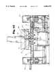
- FIGS. 1B-1Care side views of the assembly/disassembly system shown in FIG. 1A;
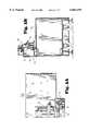
- FIGS. 2A-2Bare side and plan views respectively of a die pack feeder for use in accordance with the present invention.
- FIGS. 3A-3Care side views of a wafer handler base having a transfer mechanism which is suitable for use in the present invention
- FIG. 4is a side view of a rough die camera which may be used in the present invention.
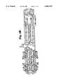
- FIGS. 5A-5Bare front and side views of a primary gripper of a robot arm
- FIG. 6illustrates a clip tray feeder for use in the present invention
- FIGS. 7A-7Billustrate plan and side views respectively of a lid feeder station suitable for use in accordance with the present invention
- FIG. 7Cis an enlarged view of the lid carousel illustrated in FIG. 7A;
- FIGS. 8A-8Bare plan and side views respectively of a lid precisor which is suitable for use in accordance with the present invention.
- FIG. 9is a plan view of the various components of an indexing mechanism for use in accurately positioning the boat in the assembly/disassembly station of the apparatus;
- FIG. 10shows a rough temporary package camera for use in accordance with the present invention
- FIGS. 11A-11Billustrate side views of a fine temporary package camera and secondary gripper which are suitable for use in accordance with the present invention
- FIGS. 12A-12Bshow an unclipping mechanism in a lowered position which is suitable for use in the disassembly process of the present invention.
- FIG. 13illustrates a secondary inverter and die precisor for use in the disassembly process of the present invention.
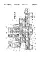
- the apparatus 10generally includes surface 42, a programmable robot arm 12 which preferably includes three arms 12a, 12b and 12c, wafer feeder station 14, die inverter 16, rough die camera 24, lid feeder station 22, lid precisor 26, fine die camera 30, predetermined assembly/disassembly position 28, clip tray feeder 50, and rough and fine temporary package cameras (not shown in FIG. 1A).
- the assembly/disassembly position 28is located along a conveyor 36 that conveys a carrier along a linear path indicated by arrow 34 between a first position, corresponding to inlet 38, and a second position, corresponding to outlet 40.
- the die, restraining device and temporary packageare assembled at assembly/disassembly position 28 as will be described more fully herein.
- each carrierenters the apparatus at the inlet 38 and then travels along the path through the assembly/disassembly position 28 where the dice are positioned within the packages in the carrier.
- the continuity between the die and temporary packageis preferably evaluated at assembly/disassembly position 28. Thereafter, the carrier is conveyed through the outlet 40 and the die is then subjected to additional testing.
- a plurality of carrierseach supporting a number of temporary packages, be continuously supplied to conveyor 36. While not meant to be limiting, this can be accomplished by the use of a carrier input elevator 38a and carrier output elevator 40a.
- a new carrieris supplied at the inlet after all packages in a previous boat located at the assembly/disassembly position 28 have been indexed through predetermined position 28. Die and restraining devices such as lids and/or clips are then supplied to the packages in the new carrier.
- Appropriate sensor and indexing assembliesare located at the inlet 38 and outlet 40 of the conveyor 36 to control the movement of carriers thereon.
- Conveyorssuch as those manufactured by Flexible Technology located in Richardson, Tex., are suitable for use in the present invention.
- Other conveyorssuch as flat belt conveyors, timing belt conveyors, walking beam mechanisms and the like are also suitable for use in the present invention.
- the conveyoris controlled by a suitable electric motor and gearing mechanism as is well-known in the art.
- a plurality of camerasis used in accordance with the present invention to insure precise placement of dice within temporary packages.
- one embodiment of the present inventionutilizes five cameras or image producers.
- a first camerais used to accurately locate the initial position of a wafer and individual die before the die is moved.
- Two additional camerasare used to locate the die and the remaining two cameras are used to locate the temporary package or device under testing (hereinafter "DUT").
- the present inventionuses rough cameras to locate the die's and DUT's general positions such that the die and DUT can each be positioned in the respective fine camera's fields of view.
- the fine camerashave fields of view in the range of about 0.0020".
- three camerasare utilized, namely, a first camera to accurately locate the position of a wafer and individual die, a die camera and a temporary package camera.
- FIGS. 1A-1Cin which an assembly system 10 for automatically positioning dice within temporary packages in accordance with the present invention is shown, wafers, which have been previously tested to select dice from a wafer map or ink dot, are positioned in wafer feeder station 14. The wafers may have previously been divided into individual dice. Alternatively, singulated dice may be supplied to die pack feeder stations 48a-48c.
- FIGS. 2A-2Billustrate side views of a 2 ⁇ 2" die pack feeder 48b.
- the die pack feeder 48binclude die pack input 60 and output 66, die shuttle 62 and pneumatic cylinder 64.
- a 4 ⁇ 4" die pack feedermay be used or as shown in FIG. 1A
- a 2 ⁇ 2" die pack feeder 48b and a 4 ⁇ 4" die pack feeder 48amay be utilized.
- Die pack feeders 48bare particularly suitable for use in the invention when singulated dice are supplied to apparatus 10. Packs are placed into input 60 and one pack is then moved onto shuttle 62 by pneumatic cylinder 64 into the workcell. Dice are then placed into or taken out of the packs. When the process is completed, shuttle 62 is moved by pneumatic cylinder 64 to output station 66.
- a wafer handler base 170 as illustrated in FIGS. 3A-3Cmay be used when the dice are supplied in wafer form.
- First camera 20 as shown in FIG. 1Ais preferably positioned over location 18. Location 18 corresponds to a die transfer position. First camera 20 is preferably located to look down at the film frame and wafer. First camera 20 first determines the exact position of the wafer on the film frame by looking for combi marks or fiducial marks on the wafer. The camera then takes a picture of each die to verify that the die is there, verify that there is no ink dot on the die, and locate the die's exact position to account for any change in position when the film frame is stretched.
- Die transfer arm 70 shown in FIGS. 3A-3C of the present inventionpicks up a die from location 18 and places the die on die inverter 16. The die is then inverted by die inverter 16, placed on die pedestal 74 and brought into view of rough die camera 24. While not meant to be limiting, the die is picked off of wafer handler base 170 or die pack feeder 48b using vacuum quills and pneumatic cylinders. The cylinders are reciprocated in such a manner that the die is transported and placed on die inverter 16.
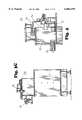
- Rough die camera 24is preferably located on surface 42 behind lid feeder station 22. As shown in FIG. 4, rough die camera 24 includes a CCD (Charge Coupled Device) camera 80, lens 82 and prism 72. Rough die camera 24, which is preferably located behind lid feeder station 22, looks up at the die through prism 72 at die inverter 16 to determine the general position or location of the die so that robot arm 12 using gripper 52 may place the die within the field of view of fine die camera 30. Prior to rough die camera 24 taking a picture, the die is preferably illuminated with backlighting. Rough die camera 24 then takes a picture of the die at die pedestal 74.
- CCDCharge Coupled Device
- the rough die pictureis analyzed utilizing a computer program to determine the rough position of the die.
- a blob finderis used to locate the centroid of the die, which is held on the pedestal arm 74.
- the blob finderanalyzes the binary (black/white) picture of the die and pedestal.
- an edge finding ruleris utilized in the negative Y direction (away from the pedestal arm) in order to locate the bottom edge of the die, as referenced in the vision window.
- a line finding boxis then used at the bottom edge of the die to locate the angle of the bottom die edge.
- the die sizeis preferably known and stored in the data file (IGES format in particular) associated with the die.
- An edge finding ruleris utilized in the negative X direction relative to the vision window. The edge finding ruler starts in the centroid of the die and is used to locate an edge of the die perpendicular to the edge located above. A line finding box is used at the perpendicular edge to locate the angle of the side edge. Once the angle and location of two perpendicular sides of the die are determined, two edge finding rulers are placed over the image. One ruler is placed across the die in order to measure the width of the die. The second ruler is placed perpendicular to the first ruler to find the length of the die to determine the exact size of the die. The center position of the die is calculated, using the average of the angles obtained above.
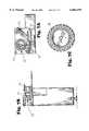
- primary gripper 52preferably includes vacuum quill 90, linear slide 94 and suction cups 92.
- Primary gripper 52which has a restraining device attached thereto, retrieves the die. While not meant to be limiting, the restraining device may be a bridge clip, a clip and lid, screw or combination thereof.
- lid transfer arm 54 shown in FIGS. 7A-7Bselects a lid from lid feeder station 22 and presents the lid to lid precisor 26. Lid precisor 26 is used to place lids in a known location.
- lid feeder station 22supports a plurality of lids in multiple stacks on a rotatable carousel 100 shown in FIG. 7A. As the lids are exhausted from each stack in the carousel, the carousel 100 rotates to present a new stack to the lid transfer arm 54. When all stacks of the carousel 100 are exhausted, the carousel 100 may be rotated away from the lid transfer arm 54 and a new carousel provided.
- FIGS. 7A-7Billustrate lid feeder station 22 while FIG. 7C depicts a plan view of a lid carousel 100 for use in the present invention.
- lid transfer arm 54selects a lid from lid feeder station 22 and presents the lid to lid precisor 26.
- FIG. 8Aillustrates a plan view of lid precisor 26 while FIG. 8B depicts a side view of lid precisor 26.
- Lid precisor 26includes a vacuum chuck 110, pneumatic cylinder 112 and precisor block 114.
- FIG. 6illustrates a clip tray feeder which is suitable for use in the present invention. More specifically, clip tray feeder 50 preferably includes an elevator 120 which carries a stack of clip trays for presentation to the machine. Each tray is individually removed and pulled into the robot's work volume by the tray presentation arms (not shown). The clip tray feeder 50 will utilize different styles of clips by utilizing optional clip trays.
- the restraining devicemay include a clip and die, a clip, lid and die or a clip/lid combination which are formed as a unit and used in conjunction with a die.
- the clipis picked up by the primary gripper 52 before the lid or die.
- the lidis placed on the vacuum chuck 110 shown in FIGS. 8A and 8B.
- the lidis placed on the vacuum chuck 110.
- the pneumatic cylinderis actuated, pressing the precisor block 114 against the lid. This action puts the lid into a location that is "known" to robot arm 12.
- the present inventionis not limited to a restraining device which includes clips and lids. Any method of restraint is possible. For example, screws, adhesives or the like may be substituted or used in addition to clips.
- the restraining deviceneed not be picked up. Rather, the restraining device may be attached to or be an integral part of the temporary package.
- Fine die camera 30is preferably located on surface 42 near conveyor 36 so that it looks sideways through a prism, up at the die.
- the surface 42 of apparatus 10may be constructed of metal, granite or a vibration isolation table. Surface 42, however, is preferably formed of granite. A granite base provides stability, which is critical for precision and accuracy.
- Fine die camera 30determines the precise location of the die and takes multiple pictures of the die such that the die bond pads and electrical interconnects can be properly aligned.
- the dieis secured and opposite corners of the die are presented to the fine die camera 30.
- the following algorithmdescribes the analysis done for each corner of the die.
- a picture of the die corneris taken.
- the binary pictureis used for all subsequent analysis steps.
- Two edge finding rulersare positioned across the width and height of the screen in order to locate the edges of the die features (Vbb ring, bond pad, etc.) specified. Once the two edges are located, line finding boxes are placed at the transition points of the edges of the die features. These are used to locate the angle of the die corner.
- the angles and pointsare used to mathematically calculate the corner point of the die etching in the field of view of the camera.
- the X and Y position of the corner pointis the only information used from the fine die picture.
- two additional picturesare taken in order to precisely determine the angle of the die.
- the picturesare taken by placing two opposite features of the die in front of the camera. The features are on the same side of the die, however. By locating two points of the etching along the same side of the die, the angle of the die relative to the angle of the gripper can be calculated.
- a pictureis taken and the binary picture is used for all subsequent analysis steps.
- An edge finding ruleris utilized from the top of the vision window in the negative Y direction in order to locate the etching of the die.
- a line finding boxis placed across the screen, perpendicular to the edge finding ruler in order to verify that the edge of the die has been located. This information is later used to position the die in proper alignment with the temporary packages.
- the carrieris conveyed along conveyor 36 between the inlet 38 and the outlet 40, but positioned to stop at predetermined assembly/disassembly position 28.
- Appropriate sensor and indexing assembliesare located at the inlet 38 and outlet 40 of conveyor 36 to control the movement of the carriers thereon.
- Each carrier or boatincludes a body portion and a pair of side rails.
- the side railspreferably include a plurality of spaced positioning holes.
- an indexing mechanism 400includes a through-beam sensor 402 mounted on one rail 404 of conveyor 36 and a locking mechanism 32 supported on the opposite rail 406.
- the through-beam sensorincludes an LED and phototransistor for counting the number of spaced positioning holes in the side rail of the carrier.
- locking mechanism 32When a predetermined number of holes have been counted, locking mechanism 32 is actuated to drive a plunger 408 into one of the positioning holes to lock the boat into position. As long as the number of holes and their relative spacing is known, it is thus possible to use the indexing mechanism 400 to control the selective movement of the boat through the assembly station regardless of the size of the boat or the number of packages therein.
- Each carriersupports a number of temporary packages. For example, carriers containing five or ten temporary packages are suitable for use in the present invention. While the number of temporary packages in a carrier may vary and while not meant to be limiting, it has been found that four temporary packages in one carrier is particularly well suited for use in accordance with the present invention.
- Temporary packagesare preferably placed in a socket container to provide electrical contact between the temporary packages and burn-in boards, load boards, and the like. While not meant to be limiting, the socket preferably raises up in assembly/disassembly position 28 to insure electrical contact. However, any method of insuring contact is sufficient.
- An electrical socket 162 shown in FIG. 12Bis then plugged into the temporary package for continuity testing to test that the die and the temporary package make electrical contact during assembly.
- Each opening in the boatincludes a pair of locking slots which secures restraining devices such as clips attached to the die to temporary packages in a boat.
- the present inventionincludes a general purpose computer control system for controlling the operation of the apparatus 10.
- the control systemincludes one or more work stations having a microprocessor having associated storage, appropriate operating system and control programs, and suitable I/O devices (such as a keyboard, mouse, display and printer).
- the apparatusfurther advantageously uses a robot arm that is controlled by a special purpose computer control system.
- the robotis a 4-axis GANTRY robot arm which is commercially available from Adept Technology, Incorporated located in San Jose, Calif.
- the robot armis controlled by associated control software routines that effect sequential movements of the robot arm in accordance with the processing steps.
- control mechanisms of the apparatusare selectively controlled by suitable actuators under the control of software programs resident in the control microprocessors. Such control mechanisms are well known in the art.
- the present inventionfurther includes two temporary package cameras or DUT cameras as illustrated in FIGS. 10 and 11A.
- a rough temporary package pictureis taken by the rough temporary package camera 130 shown in FIG. 10 to locate the temporary package in the carrier.
- the rough temporary package camera 130includes a CCD (charge coupled device) camera 132 and lens 134.
- the rough temporary package pictureis analyzed to determine the rough location of the temporary package. While not meant to be limiting, the height of the temporary package is preferably determined by a laser height sensor such as that manufactured by OMRON being placed over the temporary package.
- the rough DUT camera 130is preferably located on the Z axis of robot arm 12c and positioned to look down at the DUT or temporary package.
- the rough DUT camera 130determines the DUT's general position in the carrier so that fine DUT camera 140 (FIG. 11A) can move into correct position.
- a pictureis taken by camera 140, and the binary picture is used for all subsequent analysis steps.
- Six rulersare utilized starting at the top of the vision window in the negative Y direction. Once the rulers are placed, the closest transition is taken to be the major line of the temporary package electrical interconnects.
- a line finding boxis placed perpendicular to the rulers at the transition point in order to locate the angle of the major line of electrical interconnects. From the data (IGES) file, the following parameters are known: (a) the X distance between the fiducial mark and the major line of temporary package and (b) the side of the temporary package where the fiducial mark is located.
- a transition finding ruleris placed across the package to locate the fiducial mark.
- a blob finding boxis placed around the fiducial mark in order to precisely locate the fiducial centroid. Once the centroid is located, the center of the temporary package and the location of the electrical interconnects that the die is aligned with are calculated utilizing the data file information.
- fine temporary package or DUT camera 140as illustrated in FIG. 11A and in FIG. 11B, is positioned over the selected electrical interconnects utilizing robot arm 12.
- Fine DUT camera 140is located on the Z axis of robot arm 12 and looks down towards the DUT.
- Fine DUT camera 140determines the precise location of the DUT so that the electrical interconnects and bond pads of the die can be properly aligned with the DUT.
- Fine DUT camera 140preferably takes at least one picture at each end of the DUT.
- a secondary gripper 142such as that shown in FIGS. 11A and 11B, is also included.
- Secondary gripper 142includes a vacuum quill, linear slide and pneumatic cylinder and is used to transfer dice that are presented to the die pack feeders 48a-48c.
- Robot arm 12moves the fine DUT camera 140 over the user specified electrical interconnects. If the temporary package is built to specifications, and the rough temporary package location was successful, the chosen electrical interconnects should be placed in the center of the field of view of fine DUT camera 140.
- a pictureis taken of the electrical interconnect and a copy of the picture is created.
- the second copy of the pictureis "added” to the original picture preferably four times.
- This methodis termed GRAYSCALE ADDITION. This has the effect of isolating the temporary package features and "whiting out” the rest of the picture.
- the modified GRAYSCALE pictureis then converted to a binary picture.
- a blob finder boxis placed across the whole picture in order to locate all electrical interconnects in the picture.
- the electrical interconnect closest to the center of the pictureis selected and an arc finding circle is placed around that point with the same diameter as the electrical interconnects. This locates the center of the electrical interconnect.
- robot arm 12aligns the die and temporary package and presses the two together, thereby creating a completed assembly.
- robot arm 12preferably drives to a minimum programmed assembly locking height and tests the completed assembly for continuity. If continuity is confirmed, robot arm 12 then releases the restraining device or devices and die. If, however, continuity is not established, the robot increments to a maximum programmed force setting. If continuity is still not established, the restraining device and die are removed from the temporary package. A new package is then positioned and the fine die, rough temporary package, and fine temporary package pictures are retaken and the die and new temporary package are reassembled.
- the assembly processincludes robot arm 12 driving until physical contact is established between the die and the temporary package. After physical contact is established, robot arm 12 drives to minimum programmed assembly interlocking height. The primary gripper 52 releases the lid and/or clip and the die and then retracts to a waiting position. Electrical continuity of the assembly is tested. If the assembly has electrical continuity between the die and the temporary package, the process is completed. If electrical continuity is not established, the primary gripper 52 retrieves the die, lid and/or restraining device and awaits instruction from the operator. The operator then decides whether to retry the present package, utilize the next package, or purge the die from the system and use the next die.
- the DUT and die drawingsshould mirror one another, i.e. if one drawing were placed face-down on top of the other, the selected features should line up with one another.
- a dieBy taking pictures of the diagonal ends of each of the die and temporary package, and using an algorithm, a die can thus be precisely positioned within a temporary package in a fraction of the time required by prior art techniques. For example, prior art techniques require approximately four minutes to assemble a die in a temporary package.
- the present inventionis capable of positioning a die in a temporary package in about 30 seconds and does so in a manner which is more precise and reliable than those techniques used in accordance with the prior art.
- the methods and apparatus of the present inventionprovide for improved positioning of the die bond pads relative to the temporary package electrical interconnects than obtained using prior art techniques.
- the present inventionalso includes a disassembly process for disassembling the die from the temporary package.
- the disassembly processis substantially the opposite of the assembly process. Dice in temporary packages which have been subjected to testing enter the disassembly apparatus in boats on conveyor 36 as in the assembly process. Carriers are indexed through the apparatus 10 and are designed to proceed to predetermined disassembly position 28 as in the assembly process.
- Unclipping mechanism 150is shown. Unclipping mechanism 150 is preferably positioned along conveyor 36 near predetermined disassembly position 28. As shown in FIGS. 12A-12B, unclipping mechanism 150 includes a pneumatic parallel jaw actuator 152, clip release fingers 154, a pneumatic cylinder 158 and a linear slide 160. FIG. 12A depicts the unclipping mechanism 150 in a lowered position in which the electrical test socket disconnects from the temporary package. Prior to unclipping, the primary gripper 52 is placed by the robot arm 12 into contact with the clip and/or lid and die. The unclipping mechanism, which is raised prior to unclipping, releases the clip from the assembled package and recycled to the clip tray feeders.
- the clip, lid and dieare then removed from the temporary package by primary gripper 52 and moved to disassembly inverter 44 shown in FIGS. 1 and 13.
- the dieis placed on disassembly inverter 44 which is similar to assembly inverter 16.
- the inverted dieis then reinverted such that the die is face up on disassembly precisor 46 which is similar to lid precisor utilized in the assembly process 26.
- the dieis moved to one of the die pack feeders 48a-48c using secondary gripper 142 based on predetermined characteristics of the die. For example, dice having a certain grade or quality may be transported to feeder 48a while dice having a designated speed grade characteristic are transported to feeder 48b. Feeder 48c is generally reserved for dice which are rejected, i.e. dice which do not meet minimum characteristics. In this manner, the dice are removed and classified according to predetermined characteristics for later assembly in component packages. Additional stations may also be included to further categorize or separate the die based on various properties.
- the carrierAfter the die is removed from the boat and is being subjected to inversion by inverter 44, the carrier is simultaneously indexed such that the next package in the boat is moved into predetermined disassembly position 28. In this manner, the disassembly process is continuous. After all of the dice are removed from the carrier, the carrier continues along conveyor 36 to outlet 40 while the next carrier enters inlet 38.
Landscapes
- Engineering & Computer Science (AREA)
- Microelectronics & Electronic Packaging (AREA)
- Computer Hardware Design (AREA)
- Physics & Mathematics (AREA)
- General Physics & Mathematics (AREA)
- Power Engineering (AREA)
- Manufacturing & Machinery (AREA)
- Condensed Matter Physics & Semiconductors (AREA)
- General Engineering & Computer Science (AREA)
- Automation & Control Theory (AREA)
- Container, Conveyance, Adherence, Positioning, Of Wafer (AREA)
- Testing Of Individual Semiconductor Devices (AREA)
- Wire Bonding (AREA)
- Testing Or Measuring Of Semiconductors Or The Like (AREA)
- Supply And Installment Of Electrical Components (AREA)
Abstract
Description
Claims (14)
Priority Applications (2)
| Application Number | Priority Date | Filing Date | Title |
|---|---|---|---|
| US08/767,700US6064194A (en) | 1994-04-18 | 1996-12-17 | Method and apparatus for automatically positioning electronic dice within component packages |
| US09/234,226US6353312B1 (en) | 1994-04-18 | 1999-01-20 | Method for positioning a semiconductor die within a temporary package |
Applications Claiming Priority (2)
| Application Number | Priority Date | Filing Date | Title |
|---|---|---|---|
| US22880994A | 1994-04-18 | 1994-04-18 | |
| US08/767,700US6064194A (en) | 1994-04-18 | 1996-12-17 | Method and apparatus for automatically positioning electronic dice within component packages |
Related Parent Applications (1)
| Application Number | Title | Priority Date | Filing Date |
|---|---|---|---|
| US22880994AContinuation | 1994-04-18 | 1994-04-18 |
Related Child Applications (1)
| Application Number | Title | Priority Date | Filing Date |
|---|---|---|---|
| US09/234,226DivisionUS6353312B1 (en) | 1994-04-18 | 1999-01-20 | Method for positioning a semiconductor die within a temporary package |
Publications (1)
| Publication Number | Publication Date |
|---|---|
| US6064194Atrue US6064194A (en) | 2000-05-16 |
Family
ID=22858636
Family Applications (8)
| Application Number | Title | Priority Date | Filing Date |
|---|---|---|---|
| US08/693,398Expired - LifetimeUS5894218A (en) | 1994-04-18 | 1996-08-07 | Method and apparatus for automatically positioning electronic dice within component packages |
| US08/767,700Expired - LifetimeUS6064194A (en) | 1994-04-18 | 1996-12-17 | Method and apparatus for automatically positioning electronic dice within component packages |
| US09/170,844Expired - LifetimeUS5955877A (en) | 1994-04-18 | 1998-10-13 | Method and apparatus for automatically positioning electronic dice within component packages |
| US09/234,226Expired - Fee RelatedUS6353312B1 (en) | 1994-04-18 | 1999-01-20 | Method for positioning a semiconductor die within a temporary package |
| US09/399,640Expired - LifetimeUS6210984B1 (en) | 1994-04-18 | 1999-09-20 | Method and apparatus for automatically positioning electronic dice within component packages |
| US09/400,515Expired - LifetimeUS6150828A (en) | 1994-04-18 | 1999-09-20 | Method and apparatus for automatically positioning electronic dice with component packages |
| US09/651,490Expired - Fee RelatedUS6492187B1 (en) | 1994-04-18 | 2000-08-30 | Method for automatically positioning electronic die within component packages |
| US10/310,752Expired - Fee RelatedUS6900459B2 (en) | 1994-04-18 | 2002-12-05 | Apparatus for automatically positioning electronic dice within component packages |
Family Applications Before (1)
| Application Number | Title | Priority Date | Filing Date |
|---|---|---|---|
| US08/693,398Expired - LifetimeUS5894218A (en) | 1994-04-18 | 1996-08-07 | Method and apparatus for automatically positioning electronic dice within component packages |
Family Applications After (6)
| Application Number | Title | Priority Date | Filing Date |
|---|---|---|---|
| US09/170,844Expired - LifetimeUS5955877A (en) | 1994-04-18 | 1998-10-13 | Method and apparatus for automatically positioning electronic dice within component packages |
| US09/234,226Expired - Fee RelatedUS6353312B1 (en) | 1994-04-18 | 1999-01-20 | Method for positioning a semiconductor die within a temporary package |
| US09/399,640Expired - LifetimeUS6210984B1 (en) | 1994-04-18 | 1999-09-20 | Method and apparatus for automatically positioning electronic dice within component packages |
| US09/400,515Expired - LifetimeUS6150828A (en) | 1994-04-18 | 1999-09-20 | Method and apparatus for automatically positioning electronic dice with component packages |
| US09/651,490Expired - Fee RelatedUS6492187B1 (en) | 1994-04-18 | 2000-08-30 | Method for automatically positioning electronic die within component packages |
| US10/310,752Expired - Fee RelatedUS6900459B2 (en) | 1994-04-18 | 2002-12-05 | Apparatus for automatically positioning electronic dice within component packages |
Country Status (7)
| Country | Link |
|---|---|
| US (8) | US5894218A (en) |
| EP (2) | EP0704106B1 (en) |
| JP (1) | JP2804178B2 (en) |
| KR (1) | KR100261935B1 (en) |
| AU (1) | AU2293095A (en) |
| DE (2) | DE69534124T2 (en) |
| WO (1) | WO1995028737A1 (en) |
Cited By (19)
| Publication number | Priority date | Publication date | Assignee | Title |
|---|---|---|---|---|
| US6564979B2 (en) | 2001-07-18 | 2003-05-20 | Micron Technology, Inc. | Method and apparatus for dispensing adhesive on microelectronic substrate supports |
| US6638595B2 (en) | 2000-06-28 | 2003-10-28 | Micron Technology, Inc. | Method and apparatus for reduced flash encapsulation of microelectronic devices |
| DE10256692A1 (en)* | 2002-12-04 | 2004-06-24 | Infineon Technologies Ag | Testing method for testing connection between semiconductor element and carrier with testing effected immediately after loading semiconductor element on carrier |
| US20050012185A1 (en)* | 2003-03-04 | 2005-01-20 | Peng Neo Chee | Microelectronic component assemblies employing lead frames having reduced-thickness inner lengths |
| US6880145B1 (en)* | 2001-12-21 | 2005-04-12 | Cypress Semiconductor Corp. | Method for determining die placement based on global routing architecture |
| US20050134299A1 (en)* | 2003-12-22 | 2005-06-23 | Cram Daniel P. | System and apparatus for testing packaged devices and related methods |
| US20050167471A1 (en)* | 2003-10-07 | 2005-08-04 | Kabushiki Kaisha Shinkawa | Bonding method, bonding apparatus and bonding program |
| US20050167470A1 (en)* | 2003-10-07 | 2005-08-04 | Kabushiki Kaisha Shinkawa | Bonding pattern discrimination method, bonding pattern discrimination device and bonding pattern discrimination program |
| US20050217217A1 (en)* | 2004-04-05 | 2005-10-06 | Chin-Yu Chen | Turn-over mechanism for packaging asymmetrically shaped articles |
| US20060017177A1 (en)* | 2004-07-23 | 2006-01-26 | Seng Eric T S | Microelectronic component assemblies with recessed wire bonds and methods of making same |
| US20070045875A1 (en)* | 2005-08-30 | 2007-03-01 | Micron Technology, Inc. | Methods for wafer-level packaging of microfeature devices and microfeature devices formed using such methods |
| US20070148820A1 (en)* | 2005-12-22 | 2007-06-28 | Micron Technology, Inc. | Microelectronic devices and methods for manufacturing microelectronic devices |
| US20080006940A1 (en)* | 2006-07-05 | 2008-01-10 | Micron Technology, Inc. | Lead frames, microelectronic devices with lead frames, and methods for manufacturing lead frames and microelectronic devices with lead frames |
| US20080012110A1 (en)* | 2006-07-17 | 2008-01-17 | Micron Technology, Inc. | Microelectronic packages with leadframes, including leadframes configured for stacked die packages, and associated systems and methods |
| US20090026600A1 (en)* | 2007-07-24 | 2009-01-29 | Micron Technology, Inc. | Microelectronic die packages with metal leads, including metal leads for stacked die packages, and associated systems and methods |
| US20090045489A1 (en)* | 2007-08-16 | 2009-02-19 | Micron Technology, Inc. | Microelectronic die packages with leadframes, including leadframe-based interposer for stacked die packages, and associated systems and methods |
| US20090273359A1 (en)* | 2008-05-02 | 2009-11-05 | Micron Technology, Inc. | Electrical testing apparatus having masked sockets and associated systems and methods |
| US20100006398A1 (en)* | 2008-07-11 | 2010-01-14 | Yuan-Chi Lin | Segregating apparatus |
| TWI497641B (en)* | 2012-03-30 | 2015-08-21 | Hon Tech Inc | A picking unit, a grading device for the picking unit, and a picking method |
Families Citing this family (96)
| Publication number | Priority date | Publication date | Assignee | Title |
|---|---|---|---|---|
| EP0704106B1 (en)* | 1994-04-18 | 2003-01-29 | Micron Technology, Inc. | Method and apparatus for automatically positioning electronic die within component packages |
| DE19604833C2 (en)* | 1996-02-12 | 2000-08-10 | Karl Suss Dresden Gmbh | Arrangement for testing semiconductor structures |
| US5971256A (en) | 1997-02-05 | 1999-10-26 | Micron Technology, Inc. | Quick change precisor |
| SG72735A1 (en)* | 1997-05-06 | 2000-05-23 | Advanced Systems Automation | Test handler |
| US6085407A (en)* | 1997-08-21 | 2000-07-11 | Micron Technology, Inc. | Component alignment apparatuses and methods |
| US6401008B1 (en)* | 1998-11-18 | 2002-06-04 | Advanced Micro Devices, Inc. | Semiconductor wafer review system and method |
| AU3352700A (en)* | 1999-01-29 | 2000-08-18 | Bp Microsystems, Inc. | In-line programming system and method |
| US6580283B1 (en) | 1999-07-14 | 2003-06-17 | Aehr Test Systems | Wafer level burn-in and test methods |
| US6562636B1 (en)* | 1999-07-14 | 2003-05-13 | Aehr Test Systems | Wafer level burn-in and electrical test system and method |
| US6340895B1 (en)* | 1999-07-14 | 2002-01-22 | Aehr Test Systems, Inc. | Wafer-level burn-in and test cartridge |
| US7066708B1 (en)* | 1999-10-19 | 2006-06-27 | Micron Technology, Inc. | Methods and apparatus for retaining a tray stack having a plurality of trays for carrying microelectric devices |
| US6538425B1 (en)* | 1999-11-29 | 2003-03-25 | Fuji Machine Mfg. Co., Ltd. | Method of measuring accuracy of electric-component mounting system |
| US6485993B2 (en) | 1999-12-02 | 2002-11-26 | Teraconnect Inc. | Method of making opto-electronic devices using sacrificial devices |
| US20010007084A1 (en)* | 1999-12-30 | 2001-07-05 | Koo Ja-Hyun | Automatic wire bonder and method for implementing thereof |
| US7069102B2 (en)* | 2000-05-16 | 2006-06-27 | Texas Instruments Incorporated | System and method to customize bond programs compensating integrated circuit bonder variability |
| US7132841B1 (en)* | 2000-06-06 | 2006-11-07 | International Business Machines Corporation | Carrier for test, burn-in, and first level packaging |
| US6475826B1 (en)* | 2000-08-03 | 2002-11-05 | Advanced Micro Devices, Inc. | Method and system for detection of integrated circuit package orientation in a tape and reel system |
| US6632575B1 (en) | 2000-08-31 | 2003-10-14 | Micron Technology, Inc. | Precision fiducial |
| US6555401B2 (en)* | 2000-09-06 | 2003-04-29 | Texas Instruments Incorporated | Method of controlling bond process quality by measuring wire bond features |
| SG97164A1 (en) | 2000-09-21 | 2003-07-18 | Micron Technology Inc | Individual selective rework of defective bga solder balls |
| US6563324B1 (en)* | 2000-11-30 | 2003-05-13 | Cognex Technology And Investment Corporation | Semiconductor device image inspection utilizing rotation invariant scale invariant method |
| US6647036B1 (en)* | 2000-12-06 | 2003-11-11 | Xerox Corporation | Integration and alignment of VCSEL's with MEMS using micromachining and flip-chip techniques |
| US6707552B2 (en)* | 2000-12-18 | 2004-03-16 | Triquint Technology Holding Co. | High precision laser bar test fixture |
| US6430474B1 (en)* | 2001-04-03 | 2002-08-06 | Xerox Corporation | Tooling adapter for allowing selected manipulation of a workpiece |
| US20070152654A1 (en)* | 2001-05-14 | 2007-07-05 | Herbert Tsai | Integrated circuit (IC) transporting device for IC probe apparatus |
| MY127433A (en)* | 2001-05-29 | 2006-12-29 | Integrated Device Tech | Die bonding apparatus with automatic die and lead frame image matching system. |
| US6881593B2 (en)* | 2001-05-31 | 2005-04-19 | The Johns Hopkins University | Semiconductor die adapter and method of using |
| US6605479B1 (en)* | 2001-07-27 | 2003-08-12 | Advanced Micro Devices, Inc. | Method of using damaged areas of a wafer for process qualifications and experiments, and system for accomplishing same |
| US6764869B2 (en)* | 2001-09-12 | 2004-07-20 | Formfactor, Inc. | Method of assembling and testing an electronics module |
| US6714001B2 (en)* | 2001-11-28 | 2004-03-30 | Winbond Electronics Corporation | Dispatching method of manufacturing integrated circuit |
| US20040082013A1 (en)* | 2002-01-24 | 2004-04-29 | Regan John W | Methods for screening for substances which inhibit fp prostanoid receptor interaction with a compound having pgf2alpha activity and methods of treating cancer |
| US6913476B2 (en)* | 2002-08-06 | 2005-07-05 | Micron Technology, Inc. | Temporary, conformable contacts for microelectronic components |
| US6756796B2 (en)* | 2002-08-09 | 2004-06-29 | Texas Instruments Incorporated | Method of search and identify reference die |
| US6924653B2 (en)* | 2002-08-26 | 2005-08-02 | Micron Technology, Inc. | Selectively configurable microelectronic probes |
| US6773938B2 (en)* | 2002-08-29 | 2004-08-10 | Micron Technology, Inc. | Probe card, e.g., for testing microelectronic components, and methods for making same |
| US6879050B2 (en)* | 2003-02-11 | 2005-04-12 | Micron Technology, Inc. | Packaged microelectronic devices and methods for packaging microelectronic devices |
| US6764866B1 (en)* | 2003-02-21 | 2004-07-20 | Taiwan Semiconductor Manufacturing Co., Ltd. | System and method for qualifying multiple device under test (DUT) test head |
| US7033847B2 (en)* | 2003-03-14 | 2006-04-25 | Taiwan Semiconductor Manufacturing Co., Ltd. | Determining the maximum number of dies fitting on a semiconductor wafer |
| AU2003241977A1 (en)* | 2003-05-30 | 2005-01-21 | Advantest Corporation | Electronic component test instrument |
| AU2003242260A1 (en)* | 2003-06-06 | 2005-01-04 | Advantest Corporation | Transport device, electronic component handling device, and transporting method for electronic component handling device |
| US7222737B2 (en)* | 2003-07-03 | 2007-05-29 | Orthodyne Electronics Corporation | Die sorter with reduced mean time to convert |
| US6924655B2 (en)* | 2003-09-03 | 2005-08-02 | Micron Technology, Inc. | Probe card for use with microelectronic components, and methods for making same |
| US7458763B2 (en) | 2003-11-10 | 2008-12-02 | Blueshift Technologies, Inc. | Mid-entry load lock for semiconductor handling system |
| US7422406B2 (en)* | 2003-11-10 | 2008-09-09 | Blueshift Technologies, Inc. | Stacked process modules for a semiconductor handling system |
| US20070269297A1 (en) | 2003-11-10 | 2007-11-22 | Meulen Peter V D | Semiconductor wafer handling and transport |
| US10086511B2 (en) | 2003-11-10 | 2018-10-02 | Brooks Automation, Inc. | Semiconductor manufacturing systems |
| US7256595B2 (en)* | 2004-03-22 | 2007-08-14 | Micron Technology, Inc. | Test sockets, test systems, and methods for testing microfeature devices |
| JP4111160B2 (en) | 2004-03-26 | 2008-07-02 | 松下電器産業株式会社 | Electronic component mounting apparatus and electronic component mounting method |
| US7253089B2 (en)* | 2004-06-14 | 2007-08-07 | Micron Technology, Inc. | Microfeature devices and methods for manufacturing microfeature devices |
| US7567438B1 (en) | 2005-06-14 | 2009-07-28 | Hewlett-Packard Development Company, L.P. | Heat sink with precompressed bias member |
| US7338819B2 (en)* | 2005-06-30 | 2008-03-04 | Broadcom Corporation | System and method for matching chip and package terminals |
| SG130061A1 (en)* | 2005-08-24 | 2007-03-20 | Micron Technology Inc | Microelectronic devices and microelectronic support devices, and associated assemblies and methods |
| US7684608B2 (en)* | 2006-02-23 | 2010-03-23 | Vistech Corporation | Tape and reel inspection system |
| US7910385B2 (en)* | 2006-05-12 | 2011-03-22 | Micron Technology, Inc. | Method of fabricating microelectronic devices |
| JP4484844B2 (en)* | 2006-05-16 | 2010-06-16 | 東京エレクトロン株式会社 | Image binarization processing method, image processing apparatus, and computer program |
| US20080237961A1 (en)* | 2007-03-30 | 2008-10-02 | Honda Motor Co., Ltd. | Pad for holding blank and die assembly therewith |
| TW200848722A (en)* | 2007-06-15 | 2008-12-16 | King Yuan Electronics Co Ltd | Automatic optical inspection device |
| CN101336072B (en)* | 2007-06-29 | 2010-08-04 | 富葵精密组件(深圳)有限公司 | Surface Mount Alignment Device and Alignment Method |
| US8070473B2 (en)* | 2008-01-08 | 2011-12-06 | Stratasys, Inc. | System for building three-dimensional objects containing embedded inserts, and method of use thereof |
| US8460947B2 (en)* | 2008-09-24 | 2013-06-11 | Hewlett-Packard Development Company, L.P. | Fluid ejection device and method |
| CN102362188A (en)* | 2009-03-27 | 2012-02-22 | 爱德万测试株式会社 | Test device, test method, and production method |
| JP2011086880A (en)* | 2009-10-19 | 2011-04-28 | Advantest Corp | Electronic component mounting apparatus and method of mounting electronic component |
| US8587331B2 (en)* | 2009-12-31 | 2013-11-19 | Tommie E. Berry | Test systems and methods for testing electronic devices |
| KR101214970B1 (en) | 2010-09-17 | 2012-12-24 | 주식회사 엘지씨엔에스 | Apparatus and method for precision loading of light emitting diode wafer |
| US8680683B1 (en) | 2010-11-30 | 2014-03-25 | Triquint Semiconductor, Inc. | Wafer level package with embedded passive components and method of manufacturing |
| CN103424682A (en)* | 2012-05-16 | 2013-12-04 | 欣岩企业有限公司 | Chip testing device and testing method |
| US8903122B2 (en) | 2013-03-15 | 2014-12-02 | HGST Netherlands B.V. | Verifying a slider tray map |
| DE112014001440T5 (en)* | 2013-03-15 | 2016-01-14 | Rudolph Technologies, Inc. | Flexible handling system for semiconductor substrates |
| CN103236412B (en)* | 2013-04-10 | 2015-09-30 | 常州信息职业技术学院 | For the robot device of diode entirety carrying |
| US20140361800A1 (en)* | 2013-06-05 | 2014-12-11 | Qualcomm Incorporated | Method and apparatus for high volume system level testing of logic devices with pop memory |
| TWI540469B (en)* | 2014-04-01 | 2016-07-01 | 原相科技股份有限公司 | Electronic device with high electrostatic protection |
| US10115620B2 (en)* | 2015-08-31 | 2018-10-30 | Asm Technology Singapore Pte Ltd | Apparatus and method for adjustment of a handling device for handling electronic components |
| US10319396B2 (en) | 2016-06-16 | 2019-06-11 | Seagate Technology Llc | Transducer bar translation system and method of translating a transducer bar |
| US10933304B2 (en)* | 2016-09-26 | 2021-03-02 | Interblock Usa L.C. | System and method for regulating dice strokes in gaming system |
| DE102018100003B4 (en) | 2017-08-08 | 2020-03-12 | Taiwan Semiconductor Manufacturing Co., Ltd. | Methodology for automatic teaching of an EFEM robot |
| US10861723B2 (en)* | 2017-08-08 | 2020-12-08 | Taiwan Semiconductor Manufacturing Co., Ltd. | EFEM robot auto teaching methodology |
| US11226390B2 (en)* | 2017-08-28 | 2022-01-18 | Teradyne, Inc. | Calibration process for an automated test system |
| US10845410B2 (en) | 2017-08-28 | 2020-11-24 | Teradyne, Inc. | Automated test system having orthogonal robots |
| US10948534B2 (en) | 2017-08-28 | 2021-03-16 | Teradyne, Inc. | Automated test system employing robotics |
| US10725091B2 (en)* | 2017-08-28 | 2020-07-28 | Teradyne, Inc. | Automated test system having multiple stages |
| US10852344B2 (en) | 2017-12-12 | 2020-12-01 | Micron Technology, Inc. | Inductive testing probe apparatus for testing semiconductor die and related systems and methods |
| US10775408B2 (en) | 2018-08-20 | 2020-09-15 | Teradyne, Inc. | System for testing devices inside of carriers |
| TWI739261B (en)* | 2019-12-31 | 2021-09-11 | 萬潤科技股份有限公司 | Electronic component inspection method and electronic component inspection device |
| JP7191872B2 (en)* | 2020-01-15 | 2022-12-19 | 株式会社東芝 | Method of setting magnetic disk device and recording capacity |
| US11754622B2 (en) | 2020-10-22 | 2023-09-12 | Teradyne, Inc. | Thermal control system for an automated test system |
| US11899042B2 (en) | 2020-10-22 | 2024-02-13 | Teradyne, Inc. | Automated test system |
| US11867749B2 (en) | 2020-10-22 | 2024-01-09 | Teradyne, Inc. | Vision system for an automated test system |
| US11754596B2 (en) | 2020-10-22 | 2023-09-12 | Teradyne, Inc. | Test site configuration in an automated test system |
| US11953519B2 (en) | 2020-10-22 | 2024-04-09 | Teradyne, Inc. | Modular automated test system |
| CN113003180B (en)* | 2021-04-14 | 2023-06-23 | 深圳市标王工业设备有限公司 | IC chip loading and sorting machine |
| CN113253087B (en)* | 2021-06-18 | 2021-11-02 | 陕西开尔文测控技术有限公司 | Silicon carbide dynamic detection equipment |
| US12007411B2 (en) | 2021-06-22 | 2024-06-11 | Teradyne, Inc. | Test socket having an automated lid |
| CN113314445B (en)* | 2021-07-28 | 2021-11-23 | 苏州天准科技股份有限公司 | COB automatic assembly equipment |
| CN116329916B (en)* | 2023-05-31 | 2023-08-15 | 荣旗工业科技(苏州)股份有限公司 | Automatic feeding and assembling system and method |
| CN116741668B (en)* | 2023-06-15 | 2024-02-02 | 江苏东海半导体股份有限公司 | Multi-chip packaging and positioning device of integrated circuit and working method thereof |
| KR102725022B1 (en)* | 2024-01-23 | 2024-11-01 | 주식회사 프로이천 | Probe Test Apparatus Of Which Probe Block Is Prevented From Shaking By Restricting Tri-axial Rotation |
Citations (70)
| Publication number | Priority date | Publication date | Assignee | Title |
|---|---|---|---|---|
| JPS5541775A (en)* | 1978-09-19 | 1980-03-24 | Sharp Corp | Position aligning device in semiconductor device |
| JPS55128840A (en)* | 1979-03-27 | 1980-10-06 | Nec Corp | Method of testing lead wire bonded to semiconductor device |
| JPS55164376A (en)* | 1979-06-11 | 1980-12-22 | Nippon Telegr & Teleph Corp <Ntt> | Integrated circuit testing unit |
| US4281449A (en)* | 1979-12-21 | 1981-08-04 | Harris Corporation | Method for qualifying biased burn-in integrated circuits on a wafer level |
| US4312117A (en)* | 1977-09-01 | 1982-01-26 | Raytheon Company | Integrated test and assembly device |
| US4500836A (en)* | 1980-10-31 | 1985-02-19 | Pacific Western Systems, Inc. | Automatic wafer prober with programmable tester interface |
| US4526646A (en)* | 1983-03-03 | 1985-07-02 | Shinkawa Ltd. | Inner lead bonder |
| US4543659A (en)* | 1982-09-22 | 1985-09-24 | Tokyo Shibaura Denki Kabushiki Kaisha | Method for recognizing a pellet pattern |
| US4585991A (en)* | 1982-06-03 | 1986-04-29 | Texas Instruments Incorporated | Solid state multiprobe testing apparatus |
| US4677474A (en)* | 1984-07-02 | 1987-06-30 | Canon Kabushiki Kaisha | Wafer prober |
| US4736437A (en)* | 1982-11-22 | 1988-04-05 | View Engineering, Inc. | High speed pattern recognizer |
| US4859614A (en)* | 1979-02-19 | 1989-08-22 | Fujitsu Limited | Method for manufacturing semiconductor device with leads adhered to supporting insulator sheet |
| US4899107A (en)* | 1988-09-30 | 1990-02-06 | Micron Technology, Inc. | Discrete die burn-in for nonpackaged die |
| US4899921A (en)* | 1988-10-28 | 1990-02-13 | The American Optical Corporation | Aligner bonder |
| US4924589A (en)* | 1988-05-16 | 1990-05-15 | Leedy Glenn J | Method of making and testing an integrated circuit |
| US4929893A (en)* | 1987-10-06 | 1990-05-29 | Canon Kabushiki Kaisha | Wafer prober |
| US4992850A (en)* | 1989-02-15 | 1991-02-12 | Micron Technology, Inc. | Directly bonded simm module |
| US5002895A (en)* | 1987-04-17 | 1991-03-26 | Thomson-Csf | Wire bonding method with a frame, for connecting an electronic component for testing and mounting |
| US5008614A (en)* | 1988-10-11 | 1991-04-16 | Hewlett-Packard Company | TAB frame and process of testing same |
| US5008617A (en)* | 1989-06-20 | 1991-04-16 | Energy Conversion Devices, Inc. | Functional testing of ultra large area, ultra large scale integrated circuits |
| US5014161A (en)* | 1985-07-22 | 1991-05-07 | Digital Equipment Corporation | System for detachably mounting semiconductors on conductor substrate |
| US5023189A (en)* | 1990-05-04 | 1991-06-11 | Microwave Modules & Devices, Inc. | Method of thermal balancing RF power transistor array |
| US5052606A (en)* | 1990-06-29 | 1991-10-01 | International Business Machines Corp. | Tape automated bonding feeder |
| US5059559A (en)* | 1987-11-02 | 1991-10-22 | Hitachi, Ltd. | Method of aligning and bonding tab inner leads |
| US5073117A (en)* | 1989-03-30 | 1991-12-17 | Texas Instruments Incorporated | Flip-chip test socket adaptor and method |
| US5088190A (en)* | 1990-08-30 | 1992-02-18 | Texas Instruments Incorporated | Method of forming an apparatus for burn in testing of integrated circuit chip |
| US5103557A (en)* | 1988-05-16 | 1992-04-14 | Leedy Glenn J | Making and testing an integrated circuit using high density probe points |
| US5113565A (en)* | 1990-07-06 | 1992-05-19 | International Business Machines Corp. | Apparatus and method for inspection and alignment of semiconductor chips and conductive lead frames |
| US5123850A (en)* | 1990-04-06 | 1992-06-23 | Texas Instruments Incorporated | Non-destructive burn-in test socket for integrated circuit die |
| US5123823A (en)* | 1990-02-01 | 1992-06-23 | Mitsubishi Denki Kabushiki Kaisha | Molding device for sealing semiconductor element with resin |
| US5138434A (en)* | 1991-01-22 | 1992-08-11 | Micron Technology, Inc. | Packaging for semiconductor logic devices |
| US5145099A (en)* | 1990-07-13 | 1992-09-08 | Micron Technology, Inc. | Method for combining die attach and lead bond in the assembly of a semiconductor package |
| US5177439A (en)* | 1991-08-30 | 1993-01-05 | U.S. Philips Corporation | Probe card for testing unencapsulated semiconductor devices |
| US5238174A (en)* | 1991-11-15 | 1993-08-24 | Kulicke And Soffa Investments, Inc. | Smart indexing head for universal lead frame work station |
| US5326428A (en)* | 1993-09-03 | 1994-07-05 | Micron Semiconductor, Inc. | Method for testing semiconductor circuitry for operability and method of forming apparatus for testing semiconductor circuitry for operability |
| US5367253A (en)* | 1991-06-04 | 1994-11-22 | Micron Semiconductor, Inc. | Clamped carrier for testing of semiconductor dies |
| US5374888A (en)* | 1991-09-05 | 1994-12-20 | Tokyo Electron Kabushiki Kaisha | Electrical characteristics measurement method and measurement apparatus therefor |
| US5448165A (en)* | 1993-01-08 | 1995-09-05 | Integrated Device Technology, Inc. | Electrically tested and burned-in semiconductor die and method for producing same |
| US5451165A (en)* | 1994-07-27 | 1995-09-19 | Minnesota Mining And Manufacturing Company | Temporary package for bare die test and burn-in |
| US5463227A (en)* | 1992-06-24 | 1995-10-31 | Robotic Vision Systems, Inc. | Method for obtaining three-dimensional data from multiple parts or devices in a multi-pocketed tray |
| US5463325A (en)* | 1992-05-28 | 1995-10-31 | Rohm Co., Ltd. | Apparatus for measuring characteristics of electronic parts |
| US5467517A (en)* | 1992-05-29 | 1995-11-21 | Nippondenso Co., Ltd. | Method and system for fitting work-pieces |
| US5468157A (en)* | 1993-10-29 | 1995-11-21 | Texas Instruments Incorporated | Non-destructive interconnect system for semiconductor devices |
| US5468158A (en)* | 1993-10-29 | 1995-11-21 | Texas Instruments Incorporated | Non-destructive interconnect system for semiconductor devices |
| US5471310A (en)* | 1990-08-27 | 1995-11-28 | Sierra Research And Technology, Inc. | System for placement and mounting of fine pitch integrated circuit devices |
| US5475317A (en)* | 1993-12-23 | 1995-12-12 | Epi Technologies, Inc. | Singulated bare die tester and method of performing forced temperature electrical tests and burn-in |
| US5479105A (en)* | 1993-06-25 | 1995-12-26 | Samsung Electronics Co., Ltd. | Known-good die testing apparatus |
| US5481203A (en)* | 1994-08-05 | 1996-01-02 | Vlsi Technology, Inc. | Adapter for quad flat pack failure-analysis socket |
| US5483174A (en)* | 1992-06-10 | 1996-01-09 | Micron Technology, Inc. | Temporary connection of semiconductor die using optical alignment techniques |
| US5506510A (en)* | 1994-05-18 | 1996-04-09 | Genrad, Inc. | Adaptive alignment probe fixture for circuit board tester |
| US5506684A (en)* | 1991-04-04 | 1996-04-09 | Nikon Corporation | Projection scanning exposure apparatus with synchronous mask/wafer alignment system |
| US5516023A (en)* | 1993-12-06 | 1996-05-14 | Nec Corporation | Wire bonding apparatus |
| US5516026A (en)* | 1993-11-26 | 1996-05-14 | Toshiba Automation Co., Ltd. | Pellet bonding apparatus |
| US5517125A (en)* | 1993-07-09 | 1996-05-14 | Aehr Test Systems, Inc. | Reusable die carrier for burn-in and burn-in process |
| US5519332A (en)* | 1991-06-04 | 1996-05-21 | Micron Technology, Inc. | Carrier for testing an unpackaged semiconductor die |
| US5523586A (en)* | 1993-09-20 | 1996-06-04 | Kabushiki Kaisha Toshiba | Burn-in socket used in a burn-in test for semiconductor chips |
| US5523696A (en)* | 1993-06-14 | 1996-06-04 | International Business Machines Corp. | Method and apparatus for testing integrated circuit chips |
| US5528157A (en)* | 1994-11-15 | 1996-06-18 | National Semiconductor Corporation | Integrated circuit package for burn-in and testing of an integrated circuit die |
| US5530376A (en)* | 1993-08-25 | 1996-06-25 | Sunright Limited | Reusable carrier for burn-in/testing of non packaged die |
| US5534786A (en)* | 1994-10-14 | 1996-07-09 | Co-Operative Facility For Aging Tester Development | Burn-in and test method of semiconductor wafers and burn-in boards for use in semiconductor wafer burn-in tests |
| US5534785A (en)* | 1992-10-20 | 1996-07-09 | Fujitsu Limited | Integrated circuit bare chip carrier |
| US5537204A (en)* | 1994-11-07 | 1996-07-16 | Micron Electronics, Inc. | Automatic optical pick and place calibration and capability analysis system for assembly of components onto printed circuit boards |
| US5537051A (en)* | 1995-04-24 | 1996-07-16 | Motorola, Inc. | Apparatus for testing integrated circuits |
| US5539324A (en)* | 1988-09-30 | 1996-07-23 | Micron Technology, Inc. | Universal wafer carrier for wafer level die burn-in |
| US5541524A (en)* | 1991-08-23 | 1996-07-30 | Nchip, Inc. | Burn-in technologies for unpackaged integrated circuits |
| US5541525A (en)* | 1991-06-04 | 1996-07-30 | Micron Technology, Inc. | Carrier for testing an unpackaged semiconductor die |
| US5543725A (en)* | 1993-08-25 | 1996-08-06 | Sunright Limited | Reusable carrier for burn-in/testing on non packaged die |
| US5568057A (en)* | 1993-05-14 | 1996-10-22 | Samsung Electronics Co., Ltd. | Method for performing a burn-in test |
| US5574384A (en)* | 1995-01-31 | 1996-11-12 | Tabai Espec Corp. | Combined board construction for burn-in and burn-in equipment for use with combined board |
| US5644245A (en)* | 1993-11-24 | 1997-07-01 | Tokyo Electron Limited | Probe apparatus for inspecting electrical characteristics of a microelectronic element |
Family Cites Families (35)
| Publication number | Priority date | Publication date | Assignee | Title |
|---|---|---|---|---|
| JPS5541775B2 (en) | 1972-05-13 | 1980-10-27 | ||
| JPS55164376U (en) | 1979-05-14 | 1980-11-26 | ||
| JPS5722570A (en)* | 1980-07-02 | 1982-02-05 | Fujitsu Ltd | Automatic handling tool for parts |
| US5634267A (en)* | 1991-06-04 | 1997-06-03 | Micron Technology, Inc. | Method and apparatus for manufacturing known good semiconductor die |
| US5440240A (en)* | 1991-06-04 | 1995-08-08 | Micron Technology, Inc. | Z-axis interconnect for discrete die burn-in for nonpackaged die |
| US4985988A (en)* | 1989-11-03 | 1991-01-22 | Motorola, Inc. | Method for assembling, testing, and packaging integrated circuits |
| US4980971A (en)* | 1989-12-14 | 1991-01-01 | At&T Bell Laboratories | Method and apparatus for chip placement |
| JPH03209737A (en) | 1990-01-11 | 1991-09-12 | Tokyo Electron Ltd | Probe equipment |
| CA2044649A1 (en)* | 1990-06-19 | 1991-12-20 | Masanori Nishiguchi | Method and apparatus for packaging a semiconductor device |
| US5146661A (en)* | 1990-11-07 | 1992-09-15 | At&T Bell Laboratories | Packaged device handling method and apparatus |
| US6219908B1 (en)* | 1991-06-04 | 2001-04-24 | Micron Technology, Inc. | Method and apparatus for manufacturing known good semiconductor die |
| US5136364A (en) | 1991-06-12 | 1992-08-04 | National Semiconductor Corporation | Semiconductor die sealing |
| US5212647A (en)* | 1991-07-15 | 1993-05-18 | Preco Industries, Inc. | Die stamping press having ccd camera system for automatic 3-axis die registration |
| US5151650A (en)* | 1991-09-03 | 1992-09-29 | Motorola, Inc. | Packaged semiconductor device handler |
| US5262927A (en) | 1992-02-07 | 1993-11-16 | Lsi Logic Corporation | Partially-molded, PCB chip carrier package |
| US5416592A (en)* | 1992-03-23 | 1995-05-16 | Tokyo Electron Kabushiki Kaisha | Probe apparatus for measuring electrical characteristics of objects |
| CA2096551A1 (en)* | 1992-05-22 | 1993-11-23 | Masanori Nishiguchi | Semiconductor device |
| US5424652A (en) | 1992-06-10 | 1995-06-13 | Micron Technology, Inc. | Method and apparatus for testing an unpackaged semiconductor die |
| US5248903A (en) | 1992-09-18 | 1993-09-28 | Lsi Logic Corporation | Composite bond pads for semiconductor devices |
| US5404047A (en) | 1992-07-17 | 1995-04-04 | Lsi Logic Corporation | Semiconductor die having a high density array of composite bond pads |
| US5248797A (en) | 1992-08-13 | 1993-09-28 | American Cyanamid Company | Method for the production of 9-amino-6-demethyl-6-deoxytetracycline |
| CA2104340A1 (en) | 1992-08-31 | 1994-03-01 | Grish Chandra | Hermetic protection for integrated circuits |
| US5394100A (en) | 1993-05-06 | 1995-02-28 | Karl Suss America, Incorporated | Probe system with automatic control of contact pressure and probe alignment |
| US5633122A (en)* | 1993-08-16 | 1997-05-27 | Micron Technology, Inc. | Test fixture and method for producing a test fixture for testing unpackaged semiconductor die |
| US5640199A (en)* | 1993-10-06 | 1997-06-17 | Cognex Corporation | Automated optical inspection apparatus |
| US5561386A (en) | 1994-02-23 | 1996-10-01 | Fujitsu Limited | Chip tester with improvements in handling efficiency and measurement precision |
| US5510723A (en)* | 1994-03-01 | 1996-04-23 | Micron Custom Manufacturing, Inc. Usa | Diced semiconductor device handler |
| EP0704106B1 (en)* | 1994-04-18 | 2003-01-29 | Micron Technology, Inc. | Method and apparatus for automatically positioning electronic die within component packages |
| JP3295529B2 (en)* | 1994-05-06 | 2002-06-24 | 松下電器産業株式会社 | IC component mounting method and device |
| US5789930A (en)* | 1995-12-14 | 1998-08-04 | International Business Machine Corporation | Apparatus and method to test for known good die |
| US5888837A (en)* | 1996-04-16 | 1999-03-30 | General Electric Company | Chip burn-in and test structure and method |
| US5644979A (en)* | 1996-04-30 | 1997-07-08 | Preco Industries, Inc. | Die cutting and stamping press having simultaneous X, Y, and .O slashed. axes die registration mechanism and method |
| US6194738B1 (en)* | 1996-06-13 | 2001-02-27 | Micron Technology, Inc. | Method and apparatus for storage of test results within an integrated circuit |
| US5905850A (en)* | 1996-06-28 | 1999-05-18 | Lam Research Corporation | Method and apparatus for positioning substrates |
| US6258609B1 (en)* | 1996-09-30 | 2001-07-10 | Micron Technology, Inc. | Method and system for making known good semiconductor dice |
- 1995
- 1995-04-17EPEP95916425Apatent/EP0704106B1/ennot_activeExpired - Lifetime
- 1995-04-17JPJP7527143Apatent/JP2804178B2/ennot_activeExpired - Fee Related
- 1995-04-17DEDE69534124Tpatent/DE69534124T2/ennot_activeExpired - Lifetime
- 1995-04-17KRKR1019950705799Apatent/KR100261935B1/ennot_activeExpired - Fee Related
- 1995-04-17WOPCT/US1995/004690patent/WO1995028737A1/enactiveIP Right Grant
- 1995-04-17AUAU22930/95Apatent/AU2293095A/ennot_activeAbandoned
- 1995-04-17DEDE69529501Tpatent/DE69529501T2/ennot_activeExpired - Lifetime
- 1995-04-17EPEP02013585Apatent/EP1251550B1/ennot_activeExpired - Lifetime
- 1996
- 1996-08-07USUS08/693,398patent/US5894218A/ennot_activeExpired - Lifetime
- 1996-12-17USUS08/767,700patent/US6064194A/ennot_activeExpired - Lifetime
- 1998
- 1998-10-13USUS09/170,844patent/US5955877A/ennot_activeExpired - Lifetime
- 1999
- 1999-01-20USUS09/234,226patent/US6353312B1/ennot_activeExpired - Fee Related
- 1999-09-20USUS09/399,640patent/US6210984B1/ennot_activeExpired - Lifetime
- 1999-09-20USUS09/400,515patent/US6150828A/ennot_activeExpired - Lifetime
- 2000
- 2000-08-30USUS09/651,490patent/US6492187B1/ennot_activeExpired - Fee Related
- 2002
- 2002-12-05USUS10/310,752patent/US6900459B2/ennot_activeExpired - Fee Related
Patent Citations (73)
| Publication number | Priority date | Publication date | Assignee | Title |
|---|---|---|---|---|
| US4312117A (en)* | 1977-09-01 | 1982-01-26 | Raytheon Company | Integrated test and assembly device |
| JPS5541775A (en)* | 1978-09-19 | 1980-03-24 | Sharp Corp | Position aligning device in semiconductor device |
| US4859614A (en)* | 1979-02-19 | 1989-08-22 | Fujitsu Limited | Method for manufacturing semiconductor device with leads adhered to supporting insulator sheet |
| JPS55128840A (en)* | 1979-03-27 | 1980-10-06 | Nec Corp | Method of testing lead wire bonded to semiconductor device |
| JPS55164376A (en)* | 1979-06-11 | 1980-12-22 | Nippon Telegr & Teleph Corp <Ntt> | Integrated circuit testing unit |
| US4281449A (en)* | 1979-12-21 | 1981-08-04 | Harris Corporation | Method for qualifying biased burn-in integrated circuits on a wafer level |
| US4500836A (en)* | 1980-10-31 | 1985-02-19 | Pacific Western Systems, Inc. | Automatic wafer prober with programmable tester interface |
| US4585991A (en)* | 1982-06-03 | 1986-04-29 | Texas Instruments Incorporated | Solid state multiprobe testing apparatus |
| US4543659A (en)* | 1982-09-22 | 1985-09-24 | Tokyo Shibaura Denki Kabushiki Kaisha | Method for recognizing a pellet pattern |
| US4736437A (en)* | 1982-11-22 | 1988-04-05 | View Engineering, Inc. | High speed pattern recognizer |
| US4526646A (en)* | 1983-03-03 | 1985-07-02 | Shinkawa Ltd. | Inner lead bonder |
| US4677474A (en)* | 1984-07-02 | 1987-06-30 | Canon Kabushiki Kaisha | Wafer prober |
| US5014161A (en)* | 1985-07-22 | 1991-05-07 | Digital Equipment Corporation | System for detachably mounting semiconductors on conductor substrate |
| US5002895A (en)* | 1987-04-17 | 1991-03-26 | Thomson-Csf | Wire bonding method with a frame, for connecting an electronic component for testing and mounting |
| US4929893A (en)* | 1987-10-06 | 1990-05-29 | Canon Kabushiki Kaisha | Wafer prober |
| US5059559A (en)* | 1987-11-02 | 1991-10-22 | Hitachi, Ltd. | Method of aligning and bonding tab inner leads |
| US4924589A (en)* | 1988-05-16 | 1990-05-15 | Leedy Glenn J | Method of making and testing an integrated circuit |
| US5103557A (en)* | 1988-05-16 | 1992-04-14 | Leedy Glenn J | Making and testing an integrated circuit using high density probe points |
| US4899107A (en)* | 1988-09-30 | 1990-02-06 | Micron Technology, Inc. | Discrete die burn-in for nonpackaged die |
| US5539324A (en)* | 1988-09-30 | 1996-07-23 | Micron Technology, Inc. | Universal wafer carrier for wafer level die burn-in |
| US5008614A (en)* | 1988-10-11 | 1991-04-16 | Hewlett-Packard Company | TAB frame and process of testing same |
| US4899921A (en)* | 1988-10-28 | 1990-02-13 | The American Optical Corporation | Aligner bonder |
| US4992850A (en)* | 1989-02-15 | 1991-02-12 | Micron Technology, Inc. | Directly bonded simm module |
| US5073117A (en)* | 1989-03-30 | 1991-12-17 | Texas Instruments Incorporated | Flip-chip test socket adaptor and method |
| US5008617A (en)* | 1989-06-20 | 1991-04-16 | Energy Conversion Devices, Inc. | Functional testing of ultra large area, ultra large scale integrated circuits |
| US5288698A (en)* | 1990-02-01 | 1994-02-22 | Mitsubishi Denki Kabushiki Kaisha | Method of positioning lead frame on molding die to seal semiconductor element with resin |
| US5123823A (en)* | 1990-02-01 | 1992-06-23 | Mitsubishi Denki Kabushiki Kaisha | Molding device for sealing semiconductor element with resin |
| US5123850A (en)* | 1990-04-06 | 1992-06-23 | Texas Instruments Incorporated | Non-destructive burn-in test socket for integrated circuit die |
| US5023189A (en)* | 1990-05-04 | 1991-06-11 | Microwave Modules & Devices, Inc. | Method of thermal balancing RF power transistor array |
| US5052606A (en)* | 1990-06-29 | 1991-10-01 | International Business Machines Corp. | Tape automated bonding feeder |
| US5113565A (en)* | 1990-07-06 | 1992-05-19 | International Business Machines Corp. | Apparatus and method for inspection and alignment of semiconductor chips and conductive lead frames |
| US5145099A (en)* | 1990-07-13 | 1992-09-08 | Micron Technology, Inc. | Method for combining die attach and lead bond in the assembly of a semiconductor package |
| US5471310A (en)* | 1990-08-27 | 1995-11-28 | Sierra Research And Technology, Inc. | System for placement and mounting of fine pitch integrated circuit devices |
| US5088190A (en)* | 1990-08-30 | 1992-02-18 | Texas Instruments Incorporated | Method of forming an apparatus for burn in testing of integrated circuit chip |
| US5138434A (en)* | 1991-01-22 | 1992-08-11 | Micron Technology, Inc. | Packaging for semiconductor logic devices |
| US5506684A (en)* | 1991-04-04 | 1996-04-09 | Nikon Corporation | Projection scanning exposure apparatus with synchronous mask/wafer alignment system |
| US5541525A (en)* | 1991-06-04 | 1996-07-30 | Micron Technology, Inc. | Carrier for testing an unpackaged semiconductor die |
| US5367253A (en)* | 1991-06-04 | 1994-11-22 | Micron Semiconductor, Inc. | Clamped carrier for testing of semiconductor dies |
| US5519332A (en)* | 1991-06-04 | 1996-05-21 | Micron Technology, Inc. | Carrier for testing an unpackaged semiconductor die |
| US5541524A (en)* | 1991-08-23 | 1996-07-30 | Nchip, Inc. | Burn-in technologies for unpackaged integrated circuits |
| US5177439A (en)* | 1991-08-30 | 1993-01-05 | U.S. Philips Corporation | Probe card for testing unencapsulated semiconductor devices |
| US5374888A (en)* | 1991-09-05 | 1994-12-20 | Tokyo Electron Kabushiki Kaisha | Electrical characteristics measurement method and measurement apparatus therefor |
| US5238174A (en)* | 1991-11-15 | 1993-08-24 | Kulicke And Soffa Investments, Inc. | Smart indexing head for universal lead frame work station |
| US5463325A (en)* | 1992-05-28 | 1995-10-31 | Rohm Co., Ltd. | Apparatus for measuring characteristics of electronic parts |
| US5467517A (en)* | 1992-05-29 | 1995-11-21 | Nippondenso Co., Ltd. | Method and system for fitting work-pieces |
| US5483174A (en)* | 1992-06-10 | 1996-01-09 | Micron Technology, Inc. | Temporary connection of semiconductor die using optical alignment techniques |
| US5463227A (en)* | 1992-06-24 | 1995-10-31 | Robotic Vision Systems, Inc. | Method for obtaining three-dimensional data from multiple parts or devices in a multi-pocketed tray |
| US5534785A (en)* | 1992-10-20 | 1996-07-09 | Fujitsu Limited | Integrated circuit bare chip carrier |
| US5448165A (en)* | 1993-01-08 | 1995-09-05 | Integrated Device Technology, Inc. | Electrically tested and burned-in semiconductor die and method for producing same |
| US5568057A (en)* | 1993-05-14 | 1996-10-22 | Samsung Electronics Co., Ltd. | Method for performing a burn-in test |
| US5523696A (en)* | 1993-06-14 | 1996-06-04 | International Business Machines Corp. | Method and apparatus for testing integrated circuit chips |
| US5528159A (en)* | 1993-06-14 | 1996-06-18 | International Business Machine Corp. | Method and apparatus for testing integrated circuit chips |
| US5479105A (en)* | 1993-06-25 | 1995-12-26 | Samsung Electronics Co., Ltd. | Known-good die testing apparatus |
| US5517125A (en)* | 1993-07-09 | 1996-05-14 | Aehr Test Systems, Inc. | Reusable die carrier for burn-in and burn-in process |
| US5543725A (en)* | 1993-08-25 | 1996-08-06 | Sunright Limited | Reusable carrier for burn-in/testing on non packaged die |
| US5530376A (en)* | 1993-08-25 | 1996-06-25 | Sunright Limited | Reusable carrier for burn-in/testing of non packaged die |
| US5326428A (en)* | 1993-09-03 | 1994-07-05 | Micron Semiconductor, Inc. | Method for testing semiconductor circuitry for operability and method of forming apparatus for testing semiconductor circuitry for operability |
| US5523586A (en)* | 1993-09-20 | 1996-06-04 | Kabushiki Kaisha Toshiba | Burn-in socket used in a burn-in test for semiconductor chips |
| US5468158A (en)* | 1993-10-29 | 1995-11-21 | Texas Instruments Incorporated | Non-destructive interconnect system for semiconductor devices |
| US5571027A (en)* | 1993-10-29 | 1996-11-05 | Texas Instruments Incorporated | Non-destructive interconnect system for semiconductor devices |
| US5468157A (en)* | 1993-10-29 | 1995-11-21 | Texas Instruments Incorporated | Non-destructive interconnect system for semiconductor devices |
| US5644245A (en)* | 1993-11-24 | 1997-07-01 | Tokyo Electron Limited | Probe apparatus for inspecting electrical characteristics of a microelectronic element |
| US5516026A (en)* | 1993-11-26 | 1996-05-14 | Toshiba Automation Co., Ltd. | Pellet bonding apparatus |
| US5516023A (en)* | 1993-12-06 | 1996-05-14 | Nec Corporation | Wire bonding apparatus |
| US5475317A (en)* | 1993-12-23 | 1995-12-12 | Epi Technologies, Inc. | Singulated bare die tester and method of performing forced temperature electrical tests and burn-in |
| US5506510A (en)* | 1994-05-18 | 1996-04-09 | Genrad, Inc. | Adaptive alignment probe fixture for circuit board tester |
| US5451165A (en)* | 1994-07-27 | 1995-09-19 | Minnesota Mining And Manufacturing Company | Temporary package for bare die test and burn-in |
| US5481203A (en)* | 1994-08-05 | 1996-01-02 | Vlsi Technology, Inc. | Adapter for quad flat pack failure-analysis socket |
| US5534786A (en)* | 1994-10-14 | 1996-07-09 | Co-Operative Facility For Aging Tester Development | Burn-in and test method of semiconductor wafers and burn-in boards for use in semiconductor wafer burn-in tests |
| US5537204A (en)* | 1994-11-07 | 1996-07-16 | Micron Electronics, Inc. | Automatic optical pick and place calibration and capability analysis system for assembly of components onto printed circuit boards |
| US5528157A (en)* | 1994-11-15 | 1996-06-18 | National Semiconductor Corporation | Integrated circuit package for burn-in and testing of an integrated circuit die |
| US5574384A (en)* | 1995-01-31 | 1996-11-12 | Tabai Espec Corp. | Combined board construction for burn-in and burn-in equipment for use with combined board |
| US5537051A (en)* | 1995-04-24 | 1996-07-16 | Motorola, Inc. | Apparatus for testing integrated circuits |
Non-Patent Citations (14)
| Title |
|---|
| "Equipment, Processes and Methods for High Volume KGD Production," Third Annual Manufacturing Test Conference, pp. 150-171, Jul. 1994. |
| "Flip Chip Interconnect Technology, Process and Test Methods for Known Good Die," ETEC.(Unavailable Date). |
| * Poole, Lon, "Your Computer Revealed: Inside the Processor", MacWorld, Oct. 1992, pp. 136-142. |
| * Poole, Lon, Your Computer Revealed: Inside the Processor , MacWorld , Oct. 1992, pp. 136 142.* |
| Advertisement of Schunk Precision Workholding Systems, THK Cross roller table type VRT/VRU. (Unavailable Date).* |
| Andrews et al., Consortia for Known Good Die (KGD), Feb. 1994.* |
| Dr. Larry Schmitt, "A Vision of Vision in the Gigabit Era," Semiconductor Intenational, pp. 120-124, Jun. 1993. |
| Dr. Larry Schmitt, A Vision of Vision in the Gigabit Era, Semiconductor Intenational , pp. 120 124, Jun. 1993.* |
| Equipment, Processes and Methods for High Volume KGD Production, Third Annual Manufacturing Test Conference, pp. 150 171, Jul. 1994.* |
| Flip Chip Interconnect Technology, Process and Test Methods for Known Good Die, ETEC. (Unavailable Date).* |
| Known Good Die Workshop, Sematech , Sep. 13 & 14, 1995.* |
| Known Good Die Workshop, Sematech, Sep. 13 & 14, 1995. |
| Larry Gilg, Lo Soun Su, Mark Louis, Known Good Die (KGD) Assurance Technologies: United States Competitive Assessment, Sematech , Jul. 31, 1995.* |
| Larry Gilg, Lo-Soun Su, Mark Louis, "Known Good Die (KGD) Assurance Technologies: United States Competitive Assessment," Sematech, Jul. 31, 1995. |
Cited By (51)
| Publication number | Priority date | Publication date | Assignee | Title |
|---|---|---|---|---|
| US6638595B2 (en) | 2000-06-28 | 2003-10-28 | Micron Technology, Inc. | Method and apparatus for reduced flash encapsulation of microelectronic devices |
| US6644949B2 (en) | 2000-06-28 | 2003-11-11 | Micron Technology, Inc. | Apparatus for reduced flash encapsulation of microelectronic devices |
| US6564979B2 (en) | 2001-07-18 | 2003-05-20 | Micron Technology, Inc. | Method and apparatus for dispensing adhesive on microelectronic substrate supports |
| US6880145B1 (en)* | 2001-12-21 | 2005-04-12 | Cypress Semiconductor Corp. | Method for determining die placement based on global routing architecture |
| DE10256692A1 (en)* | 2002-12-04 | 2004-06-24 | Infineon Technologies Ag | Testing method for testing connection between semiconductor element and carrier with testing effected immediately after loading semiconductor element on carrier |
| US20040155646A1 (en)* | 2002-12-04 | 2004-08-12 | Infineon Technologies Ag | Testing apparatus and method for testing the contacting between a semiconductor device and a carrier |
| US7425470B2 (en) | 2003-03-04 | 2008-09-16 | Micron Technology, Inc. | Microelectronic component assemblies employing lead frames having reduced-thickness inner lengths |
| US20050012185A1 (en)* | 2003-03-04 | 2005-01-20 | Peng Neo Chee | Microelectronic component assemblies employing lead frames having reduced-thickness inner lengths |
| US7691680B2 (en) | 2003-03-04 | 2010-04-06 | Micron Technologies, Inc. | Method of fabricating microelectronic component assemblies employing lead frames having reduced-thickness inner lengths |
| US20050167471A1 (en)* | 2003-10-07 | 2005-08-04 | Kabushiki Kaisha Shinkawa | Bonding method, bonding apparatus and bonding program |
| US7224829B2 (en)* | 2003-10-07 | 2007-05-29 | Kabushiki Kaisha Shinkawa | Bonding pattern discrimination method, bonding pattern discrimination device and bonding pattern discrimination program |
| US20050167470A1 (en)* | 2003-10-07 | 2005-08-04 | Kabushiki Kaisha Shinkawa | Bonding pattern discrimination method, bonding pattern discrimination device and bonding pattern discrimination program |
| US7209583B2 (en)* | 2003-10-07 | 2007-04-24 | Kabushiki Kaisha Shinkawa | Bonding method, bonding apparatus and bonding program |
| US7043388B2 (en) | 2003-12-22 | 2006-05-09 | Micron Technology, Inc. | System and apparatus for testing packaged devices and related methods |
| US20050134299A1 (en)* | 2003-12-22 | 2005-06-23 | Cram Daniel P. | System and apparatus for testing packaged devices and related methods |
| US20050217217A1 (en)* | 2004-04-05 | 2005-10-06 | Chin-Yu Chen | Turn-over mechanism for packaging asymmetrically shaped articles |
| US20080164591A1 (en)* | 2004-07-23 | 2008-07-10 | Micron Technology, Inc. | Microelectronic component assemblies with recessed wire bonds and methods of making same |
| US7250328B2 (en) | 2004-07-23 | 2007-07-31 | Micron Technology, Inc. | Microelectronic component assemblies with recessed wire bonds and methods of making same |
| US7365424B2 (en) | 2004-07-23 | 2008-04-29 | Micron Technology, Inc. | Microelectronic component assemblies with recessed wire bonds and methods of making same |
| US20060208366A1 (en)* | 2004-07-23 | 2006-09-21 | Micron Technology, Inc. | Microelectronic component assemblies with recessed wire bonds and methods of making same |
| US20060017177A1 (en)* | 2004-07-23 | 2006-01-26 | Seng Eric T S | Microelectronic component assemblies with recessed wire bonds and methods of making same |
| US7696003B2 (en) | 2004-07-23 | 2010-04-13 | Micron Technology, Inc. | Microelectronic component assemblies with recessed wire bonds and methods of making same |
| US20070045875A1 (en)* | 2005-08-30 | 2007-03-01 | Micron Technology, Inc. | Methods for wafer-level packaging of microfeature devices and microfeature devices formed using such methods |
| US7807505B2 (en) | 2005-08-30 | 2010-10-05 | Micron Technology, Inc. | Methods for wafer-level packaging of microfeature devices and microfeature devices formed using such methods |
| US8704380B2 (en) | 2005-08-30 | 2014-04-22 | Micron Technology, Inc. | Methods for wafer-level packaging of microfeature devices and microfeature devices formed using such methods |
| US20100327462A1 (en)* | 2005-08-30 | 2010-12-30 | Micron Technology, Inc. | Methods for wafer-level packaging of microfeature devices and microfeature devices formed using such methods |
| US20070148820A1 (en)* | 2005-12-22 | 2007-06-28 | Micron Technology, Inc. | Microelectronic devices and methods for manufacturing microelectronic devices |
| US20080006940A1 (en)* | 2006-07-05 | 2008-01-10 | Micron Technology, Inc. | Lead frames, microelectronic devices with lead frames, and methods for manufacturing lead frames and microelectronic devices with lead frames |
| US20080012110A1 (en)* | 2006-07-17 | 2008-01-17 | Micron Technology, Inc. | Microelectronic packages with leadframes, including leadframes configured for stacked die packages, and associated systems and methods |
| US7692931B2 (en) | 2006-07-17 | 2010-04-06 | Micron Technology, Inc. | Microelectronic packages with leadframes, including leadframes configured for stacked die packages, and associated systems and methods |
| US8869387B2 (en) | 2006-07-17 | 2014-10-28 | Micron Technology, Inc. | Methods for making microelectronic die systems |
| US20100173454A1 (en)* | 2006-07-17 | 2010-07-08 | Micron Technology, Inc. | Microelectronic packages with leadframes, including leadframes configured for stacked die packages, and associated systems and methods |
| US20090026600A1 (en)* | 2007-07-24 | 2009-01-29 | Micron Technology, Inc. | Microelectronic die packages with metal leads, including metal leads for stacked die packages, and associated systems and methods |
| US8536702B2 (en) | 2007-07-24 | 2013-09-17 | Micron Technology, Inc. | Microelectronic die packages with metal leads, including metal leads for stacked die packages, and associated systems and methods |
| US10396059B2 (en) | 2007-07-24 | 2019-08-27 | Micron Technology, Inc. | Microelectronic die packages with metal leads, including metal leads for stacked die packages, and associated systems and methods |
| US10056359B2 (en) | 2007-07-24 | 2018-08-21 | Micron Technology, Inc. | Microelectronic die packages with metal leads, including metal leads for stacked die packages, and associated systems and methods |
| US20110068454A1 (en)* | 2007-07-24 | 2011-03-24 | Micron Technology, Inc. | Microelectronic die packages with metal leads, including metal leads for stacked die packages, and associated systems and methods |
| US7843050B2 (en) | 2007-07-24 | 2010-11-30 | Micron Technology, Inc. | Microelectronic die packages with metal leads, including metal leads for stacked die packages, and associated systems and methods |
| US9653444B2 (en) | 2007-07-24 | 2017-05-16 | Micron Technology, Inc. | Microelectronic die packages with metal leads, including metal leads for stacked die packages, and associated systems and methods |
| US9165910B2 (en) | 2007-07-24 | 2015-10-20 | Micron Technology, Inc. | Microelectronic die packages with metal leads, including metal leads for stacked die packages, and associated systems and methods |
| US8198720B2 (en) | 2007-07-24 | 2012-06-12 | Micron Technology, Inc. | Microelectronic die packages with metal leads, including metal leads for stacked die packages, and associated systems and methods |
| US8906744B2 (en) | 2007-07-24 | 2014-12-09 | Micron Technology, Inc. | Microelectronic die packages with metal leads, including metal leads for stacked die packages, and associated systems and methods |
| US7947529B2 (en) | 2007-08-16 | 2011-05-24 | Micron Technology, Inc. | Microelectronic die packages with leadframes, including leadframe-based interposer for stacked die packages, and associated systems and methods |
| US20090045489A1 (en)* | 2007-08-16 | 2009-02-19 | Micron Technology, Inc. | Microelectronic die packages with leadframes, including leadframe-based interposer for stacked die packages, and associated systems and methods |
| US8525320B2 (en) | 2007-08-16 | 2013-09-03 | Micron Technology, Inc. | Microelectronic die packages with leadframes, including leadframe-based interposer for stacked die packages, and associated systems and methods |
| US20110215453A1 (en)* | 2007-08-16 | 2011-09-08 | Micron Technology, Inc. | Microelectronic die packages with leadframes, including leadframe-based interposer for stacked die packages, and associated systems and methods |
| US20090273359A1 (en)* | 2008-05-02 | 2009-11-05 | Micron Technology, Inc. | Electrical testing apparatus having masked sockets and associated systems and methods |
| US7857646B2 (en) | 2008-05-02 | 2010-12-28 | Micron Technology, Inc. | Electrical testing apparatus having masked sockets and associated systems and methods |
| US8066113B2 (en)* | 2008-07-11 | 2011-11-29 | King Yuan Electronics Co., Ltd. | Segregating apparatus |
| US20100006398A1 (en)* | 2008-07-11 | 2010-01-14 | Yuan-Chi Lin | Segregating apparatus |
| TWI497641B (en)* | 2012-03-30 | 2015-08-21 | Hon Tech Inc | A picking unit, a grading device for the picking unit, and a picking method |
Also Published As
| Publication number | Publication date |
|---|---|
| DE69534124T2 (en) | 2006-05-04 |
| US6353312B1 (en) | 2002-03-05 |
| AU2293095A (en) | 1995-11-10 |
| US6492187B1 (en) | 2002-12-10 |
| DE69534124D1 (en) | 2005-05-04 |
| EP0704106A1 (en) | 1996-04-03 |
| US5894218A (en) | 1999-04-13 |
| US6900459B2 (en) | 2005-05-31 |
| EP1251550A1 (en) | 2002-10-23 |
| EP1251550B1 (en) | 2005-03-30 |
| US6210984B1 (en) | 2001-04-03 |
| US20030088973A1 (en) | 2003-05-15 |
| US5955877A (en) | 1999-09-21 |
| WO1995028737A1 (en) | 1995-10-26 |
| US6150828A (en) | 2000-11-21 |
| DE69529501D1 (en) | 2003-03-06 |
| DE69529501T2 (en) | 2003-12-11 |
| KR100261935B1 (en) | 2000-07-15 |
| EP0704106B1 (en) | 2003-01-29 |
| JP2804178B2 (en) | 1998-09-24 |
| JPH08510601A (en) | 1996-11-05 |
Similar Documents
| Publication | Publication Date | Title |
|---|---|---|
| US6064194A (en) | Method and apparatus for automatically positioning electronic dice within component packages | |
| KR101683576B1 (en) | Wafer handler comprising a vision system | |
| CN218004799U (en) | Full-automatic batch chip testing device | |
| EP3403108B1 (en) | Method and device for loading and unloading devices under test into a tester by flipping | |
| JPH0567655A (en) | Characteristic inspection device for semiconductor devices | |
| KR20100110835A (en) | A method and device for aligning components | |
| US20110038694A1 (en) | Semiconductor die sorter for wafer level packaging | |
| JP6571176B2 (en) | Component mounter and component supply method for component mounter | |
| JP4233705B2 (en) | Die bonding method and die bonding equipment | |
| US7489156B2 (en) | Method for testing micro SD devices using test circuits | |
| CN222112635U (en) | Double-clamping-disc testing system | |
| TW202347582A (en) | Method and apparatus for multiple axis direct transfers of semiconductor devices | |
| CN101368993B (en) | Equipment for testing a plurality of micro-digital security devices | |
| US7489155B2 (en) | Method for testing plurality of system-in-package devices using plurality of test circuits | |
| JPH08261736A (en) | Semiconductor insertion / extraction device | |
| CN222147639U (en) | Automatic module testing system | |
| JP2001021617A (en) | Method for carrying electronic part and its device | |
| CN101777508B (en) | Defective circuit chip sorting system and method thereof | |
| JPH02210274A (en) | Handler for integrated circuit device tester and its handling method | |
| JPH01202832A (en) | Prober for manufacture of semiconductor | |
| JPS6031636B2 (en) | Flat type electronic component transfer and characteristic sorting device | |
| JPH0547903A (en) | Positioning equipment for semiconductor device | |
| JPH02272371A (en) | Semiconductor checking device | |
| HK1148387B (en) | A method and device for aligning components |
Legal Events
| Date | Code | Title | Description |
|---|---|---|---|
| STCF | Information on status: patent grant | Free format text:PATENTED CASE | |
| CC | Certificate of correction | ||
| FPAY | Fee payment | Year of fee payment:4 | |
| FPAY | Fee payment | Year of fee payment:8 | |
| FEPP | Fee payment procedure | Free format text:PAYOR NUMBER ASSIGNED (ORIGINAL EVENT CODE: ASPN); ENTITY STATUS OF PATENT OWNER: LARGE ENTITY | |
| FPAY | Fee payment | Year of fee payment:12 | |
| AS | Assignment | Owner name:U.S. BANK NATIONAL ASSOCIATION, AS COLLATERAL AGENT, CALIFORNIA Free format text:SECURITY INTEREST;ASSIGNOR:MICRON TECHNOLOGY, INC.;REEL/FRAME:038669/0001 Effective date:20160426 Owner name:U.S. BANK NATIONAL ASSOCIATION, AS COLLATERAL AGEN Free format text:SECURITY INTEREST;ASSIGNOR:MICRON TECHNOLOGY, INC.;REEL/FRAME:038669/0001 Effective date:20160426 | |
| AS | Assignment | Owner name:MORGAN STANLEY SENIOR FUNDING, INC., AS COLLATERAL AGENT, MARYLAND Free format text:PATENT SECURITY AGREEMENT;ASSIGNOR:MICRON TECHNOLOGY, INC.;REEL/FRAME:038954/0001 Effective date:20160426 Owner name:MORGAN STANLEY SENIOR FUNDING, INC., AS COLLATERAL Free format text:PATENT SECURITY AGREEMENT;ASSIGNOR:MICRON TECHNOLOGY, INC.;REEL/FRAME:038954/0001 Effective date:20160426 | |
| AS | Assignment | Owner name:U.S. BANK NATIONAL ASSOCIATION, AS COLLATERAL AGENT, CALIFORNIA Free format text:CORRECTIVE ASSIGNMENT TO CORRECT THE REPLACE ERRONEOUSLY FILED PATENT #7358718 WITH THE CORRECT PATENT #7358178 PREVIOUSLY RECORDED ON REEL 038669 FRAME 0001. ASSIGNOR(S) HEREBY CONFIRMS THE SECURITY INTEREST;ASSIGNOR:MICRON TECHNOLOGY, INC.;REEL/FRAME:043079/0001 Effective date:20160426 Owner name:U.S. BANK NATIONAL ASSOCIATION, AS COLLATERAL AGEN Free format text:CORRECTIVE ASSIGNMENT TO CORRECT THE REPLACE ERRONEOUSLY FILED PATENT #7358718 WITH THE CORRECT PATENT #7358178 PREVIOUSLY RECORDED ON REEL 038669 FRAME 0001. ASSIGNOR(S) HEREBY CONFIRMS THE SECURITY INTEREST;ASSIGNOR:MICRON TECHNOLOGY, INC.;REEL/FRAME:043079/0001 Effective date:20160426 | |
| AS | Assignment | Owner name:MICRON TECHNOLOGY, INC., IDAHO Free format text:RELEASE BY SECURED PARTY;ASSIGNOR:U.S. BANK NATIONAL ASSOCIATION, AS COLLATERAL AGENT;REEL/FRAME:047243/0001 Effective date:20180629 | |
| AS | Assignment | Owner name:MICRON TECHNOLOGY, INC., IDAHO Free format text:RELEASE BY SECURED PARTY;ASSIGNOR:MORGAN STANLEY SENIOR FUNDING, INC., AS COLLATERAL AGENT;REEL/FRAME:050937/0001 Effective date:20190731 |