US6064078A - Formation of group III-V nitride films on sapphire substrates with reduced dislocation densities - Google Patents
Formation of group III-V nitride films on sapphire substrates with reduced dislocation densitiesDownload PDFInfo
- Publication number
- US6064078A US6064078AUS09/083,137US8313798AUS6064078AUS 6064078 AUS6064078 AUS 6064078AUS 8313798 AUS8313798 AUS 8313798AUS 6064078 AUS6064078 AUS 6064078A
- Authority
- US
- United States
- Prior art keywords
- interlayer
- group iii
- substrate
- atoms
- group
- Prior art date
- Legal status (The legal status is an assumption and is not a legal conclusion. Google has not performed a legal analysis and makes no representation as to the accuracy of the status listed.)
- Expired - Lifetime
Links
Images


Classifications
- H—ELECTRICITY
- H10—SEMICONDUCTOR DEVICES; ELECTRIC SOLID-STATE DEVICES NOT OTHERWISE PROVIDED FOR
- H10H—INORGANIC LIGHT-EMITTING SEMICONDUCTOR DEVICES HAVING POTENTIAL BARRIERS
- H10H20/00—Individual inorganic light-emitting semiconductor devices having potential barriers, e.g. light-emitting diodes [LED]
- H10H20/01—Manufacture or treatment
- H10H20/011—Manufacture or treatment of bodies, e.g. forming semiconductor layers
- H10H20/013—Manufacture or treatment of bodies, e.g. forming semiconductor layers having light-emitting regions comprising only Group III-V materials
- H10H20/0133—Manufacture or treatment of bodies, e.g. forming semiconductor layers having light-emitting regions comprising only Group III-V materials with a substrate not being Group III-V materials
- H10H20/01335—Manufacture or treatment of bodies, e.g. forming semiconductor layers having light-emitting regions comprising only Group III-V materials with a substrate not being Group III-V materials the light-emitting regions comprising nitride materials
- H—ELECTRICITY
- H01—ELECTRIC ELEMENTS
- H01L—SEMICONDUCTOR DEVICES NOT COVERED BY CLASS H10
- H01L21/00—Processes or apparatus adapted for the manufacture or treatment of semiconductor or solid state devices or of parts thereof
- H01L21/02—Manufacture or treatment of semiconductor devices or of parts thereof
- H01L21/02104—Forming layers
- H01L21/02365—Forming inorganic semiconducting materials on a substrate
- H01L21/02367—Substrates
- H01L21/0237—Materials
- H01L21/0242—Crystalline insulating materials
- H—ELECTRICITY
- H01—ELECTRIC ELEMENTS
- H01L—SEMICONDUCTOR DEVICES NOT COVERED BY CLASS H10
- H01L21/00—Processes or apparatus adapted for the manufacture or treatment of semiconductor or solid state devices or of parts thereof
- H01L21/02—Manufacture or treatment of semiconductor devices or of parts thereof
- H01L21/02104—Forming layers
- H01L21/02365—Forming inorganic semiconducting materials on a substrate
- H01L21/02436—Intermediate layers between substrates and deposited layers
- H01L21/02439—Materials
- H01L21/02455—Group 13/15 materials
- H01L21/02458—Nitrides
- H—ELECTRICITY
- H01—ELECTRIC ELEMENTS
- H01L—SEMICONDUCTOR DEVICES NOT COVERED BY CLASS H10
- H01L21/00—Processes or apparatus adapted for the manufacture or treatment of semiconductor or solid state devices or of parts thereof
- H01L21/02—Manufacture or treatment of semiconductor devices or of parts thereof
- H01L21/02104—Forming layers
- H01L21/02365—Forming inorganic semiconducting materials on a substrate
- H01L21/02436—Intermediate layers between substrates and deposited layers
- H01L21/02439—Materials
- H01L21/02491—Conductive materials
- H—ELECTRICITY
- H01—ELECTRIC ELEMENTS
- H01L—SEMICONDUCTOR DEVICES NOT COVERED BY CLASS H10
- H01L21/00—Processes or apparatus adapted for the manufacture or treatment of semiconductor or solid state devices or of parts thereof
- H01L21/02—Manufacture or treatment of semiconductor devices or of parts thereof
- H01L21/02104—Forming layers
- H01L21/02365—Forming inorganic semiconducting materials on a substrate
- H01L21/02436—Intermediate layers between substrates and deposited layers
- H01L21/02494—Structure
- H01L21/02496—Layer structure
- H01L21/02499—Monolayers
- H—ELECTRICITY
- H01—ELECTRIC ELEMENTS
- H01L—SEMICONDUCTOR DEVICES NOT COVERED BY CLASS H10
- H01L21/00—Processes or apparatus adapted for the manufacture or treatment of semiconductor or solid state devices or of parts thereof
- H01L21/02—Manufacture or treatment of semiconductor devices or of parts thereof
- H01L21/02104—Forming layers
- H01L21/02365—Forming inorganic semiconducting materials on a substrate
- H01L21/02436—Intermediate layers between substrates and deposited layers
- H01L21/02494—Structure
- H01L21/02496—Layer structure
- H01L21/02502—Layer structure consisting of two layers
- H—ELECTRICITY
- H01—ELECTRIC ELEMENTS
- H01L—SEMICONDUCTOR DEVICES NOT COVERED BY CLASS H10
- H01L21/00—Processes or apparatus adapted for the manufacture or treatment of semiconductor or solid state devices or of parts thereof
- H01L21/02—Manufacture or treatment of semiconductor devices or of parts thereof
- H01L21/02104—Forming layers
- H01L21/02365—Forming inorganic semiconducting materials on a substrate
- H01L21/02518—Deposited layers
- H01L21/02521—Materials
- H01L21/02538—Group 13/15 materials
- H01L21/0254—Nitrides
Definitions
- This inventionis directed to the field of semiconductors. More particularly, this invention is directed to group III-V nitride epitaxial semiconductor films for use in blue light emitting optoelectronic devices and also to a method of forming structures including the semiconductor films.
- High-efficiency solid-state optoelectronic devices based on group III-V nitrideshave a sufficiently wide bandgap for short-wavelength visible light emission.
- the Al--Ga--In--N systemhas a bandgap which covers the entire visible spectrum.
- III-V nitrideshave been used in short-wavelength light-emitting diode (LED) devices to provide bright green-to-ultraviolet light at high efficiencies.
- LEDlight-emitting diode
- InGaNis used in green and blue LEDs. LEDs cover all three primary colors of the spectrum (red, green and blue) and accordingly can be used in various combinations to produce any color.
- III-V nitrideshave also been used in diode lasers that operate at room temperature and emit visible light in the blue-violet range under continuous operation. These diode lasers emit coherent radiation and focus light into smaller spots, enabling higher-density optical data storage and higher-resolution printing. Blue semiconductor lasers are especially promising for such applications due to their reduced wavelength. These lasers can potentially be combined with green and red lasers to create projection displays and color film printers.
- III-V nitridesprovide the important advantage of having a strong chemical bond which makes them highly stable and resistant to degradation under high electric current and intense light illumination conditions that are present at the active regions of optoelectronic devices. These materials are also resistant to dislocation formation once grown.
- III-V nitridesDue to the high growth temperatures of III-V nitrides, there are presently only a limited number of known substrates suitable for supporting nitride film growth.
- the most commonly used substrate materialsare sapphire and silicon carbide. These materials have significantly different lattice parameters and thermal expansion coefficients than the III-V nitrides. Consequently, the interfaces formed between the substrates and nitrides lack coherence, resulting in increased interface strain and interface energy, and diminished film wetting. These factors largely affect the nitride film growth process and the quality of the resulting nitride films. For example, the growth process of III-V nitrides on sapphire using known processes is highly three-dimensional.
- III-V nitride film growthoccurs initially by the formation of discrete three-dimensional nitride islands on the substrate. These islands grow and coalesce with each other. Lattice matching is poor at the regions of the film at which the islands coalesce. High dislocation densities are generated at these regions. Dislocation arrays in the nitride film adversely affect the optoelectronic properties of devices fabricated on the nitride films by affecting carrier recombination processes in the active regions of the devices, and ultimately reducing emitted light intensities and device efficiencies.
- Two-dimensional growth of III-V nitride films on substratesis desirable to reduce the dislocation densities in the films.
- two-dimensional growthis inhibited by the high interface energy between the substrates and the films.
- Two-dimensional growthbegins only after the islands coalesce and dislocations form.
- Forming buffer layers on sapphire substratesis known to enhance two-dimensional nucleation of GaN films on the buffer layers.
- improved group III-V nitride films grown on substratesare desirable.
- improved group III-V nitride filmsare desired that have reduced dislocation densities and improved electrical properties and can be used in optoelectronic devices to provide enhanced device performance.
- This inventionprovides group III-V nitride films grown on substrates that have reduced dislocation densities.
- This inventionalso provides a method of forming the improved group III-V nitride films on substrates.
- the group III-V nitride filmscan be used in light emitting devices including LEDs and diode lasers to improve device performance.
- a structure according to an aspect of this inventioncomprises a substrate; an interlayer on the substrate; and a group III-V nitride film on the interlayer.
- the interlayerprovides approximate or even exact local charge neutrality at the interface between the substrate and the group III-V nitride films. This charge neutrality promotes two-dimensional growth of the group III-V nitride film, resulting in reduced dislocation densities and improved electrical and optical properties of the films.
- the substratetypically comprises sapphire.
- the interlayercomprises atoms of at least one group II element. Group II elements have a valence of two.
- the interlayercomprises a sufficient number of atoms of the group II elements to achieve approximate or exact local charge neutrality at the interface between the substrate and the group III-V nitride film.
- This single layer of atomshas an areal density (atoms/area) that is less than or equal to that of one "monolayer", where a "monolayer” is defined herein as a layer one atom layer thick and having an areal density equivalent to the areal density of nitrogen atoms in a (0001) plane of unstrained bulk AlN.
- the interlayer atomsprovide local charge neutrality by donating electrons to oxygen atoms in the sapphire substrate and to nitrogen atoms in the group III-V nitride at the interface region.
- exact local charge neutralitycan be achieved by replacing some of the group II element atoms with atoms of one or more group III elements.
- Group III elementshave a valence of three and thus donate one additional electron to the oxygen atoms of the sapphire substrates, compared to the group II elements.
- the group III-V nitride filmscan comprise, for example, binary compounds such as GaN and AlN, ternary alloys such as AlGaN and InGaN, and quaternary alloys.
- a structure according to another aspect of this inventioncomprises a substrate; an interlayer on the substrate; a group III-V nitride buffer layer on the interlayer; and a group III-V nitride epitaxial film on the buffer layer.
- the group III-V nitride epitaxial filmsreplicate the defect structure of the buffer layer. Accordingly, because the defect (dislocation) structure of the buffer layer is improved by the provision of the interlayer on the substrate, the defect structures of the epitaxial films grown on the buffer layer can be improved as well.
- the interlayercan be formed by depositing atoms of group II, and possibly group III, elements using different techniques.
- the atomscan be deposited as individual atoms, as ions, or as oxides of group II, and possibly group III, elements.
- the improved group III-V nitride films formed according to this inventioncan be used in optoelectronic devices to improve device performance.
- FIG. 1is a cross-sectional view of a structure comprising a substrate, an interlayer on the substrate, and a group III-V nitride film on the interlayer, according to an embodiment of this invention
- FIG. 2is a cross-sectional view of a structure comprising a substrate, an interlayer on the substrate, and a buffer layer disposed between the interlayer and a group III-V nitride film, according to another embodiment of this invention
- FIG. 3illustrates an exemplary atomic arrangement at an Al 2 O 3 (0001)-AlN (0001) interface of a structure according to an embodiment of this invention.
- FIG. 4illustrates an exemplary atomic arrangement at an Al 2 O 3 (1120)-AlN (0001) interface of a structure according to an embodiment of this invention.
- This inventionis directed to group III-V nitride films formed on substrates for optoelectronic device applications, and to a method of forming the group III-V nitride films on substrates.
- Group III-V nitridescomprise elements selected from groups III and V of the periodic table. There are known group III-V nitride compounds and alloys comprising group III elements including Al, Ga and In and the group V element N. These materials are deposited on substrates to produce layered structures usable in optoelectronic devices, including LEDs and diode lasers. These devices emit visible light over a wide range of wavelengths.
- the performance of the optoelectronic devicesdepends on the quality of the group III-V nitride films formed on the substrates.
- An important structural characteristic of the group III-V nitride films that affects their qualityis dislocation density.
- This inventionprovides improved group III-V nitride films that have reduced dislocation densities. These films can be used in optoelectronic devices to provide enhanced device performance.
- this inventionprovides structures comprising improved group III-V nitride films on substrates.
- the structuresare formed by depositing an interlayer on substrates and then depositing group III-V nitride films on the substrates.
- the interlayerimproves the quality of the group III-V nitride films grown on the substrates.
- the interlayercomprises approximately one monolayer of atoms having a valence that provides an effective number of electrons at an interface formed between the substrates and group III-V nitride films to improve the quality of the films and of subsequently formed films on the substrate.
- a "monolayer”is defined herein as a layer one atom thick that has an areal density equivalent to the areal density of nitrogen atoms in a (0001) plane of unstrained bulk AlN.
- the interlayerdonates electrons to achieve approximate or even exact local charge neutrality at the interface. This charge neutrality affects the interface energy, improving the wetting of the substrate by the group III-V nitride films. Improved wetting promotes two-dimensional growth of the group III-V nitride films on the substrates, resulting in group III-V nitride films having lower dislocation densities than three-dimensionally grown films formed according to known processes.
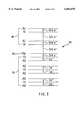
- FIG. 1illustrates an embodiment of a layered structure 10 that can be formed according to an aspect of this invention.
- the structurecomprises a substrate 12, an interlayer 14 formed on the substrate 12, and a group III-V nitride film 16 formed on the interlayer 14.
- the substrate 12is typically a sapphire substrate. Such sapphire substrates are referred to herein as the sapphire substrate 12. Suitable sapphire substrates include A-plane and c-plane oriented sapphire single crystals. The A-plane is the (1120) plane and the c-plane is the (0001) plane.
- the interlayer 14comprises atoms of at least one element selected from group II elements of the periodic table.
- the group II atomshave a valence of two. Suitable group II elements include, but are not limited to, Zn, Mg, Ca and Cd. As described in greater detail below, the group II elements have an electronic configuration that enables them to be used in the structure 10 to achieve local electronic matching and charge neutrality at the interface between the substrate and group III-V nitride films grown on the substrate.
- the group II atoms in the interlayer 14bond ironically both to oxygen atoms in the sapphire substrate 12 and to nitrogen atoms of the group III-V nitride film 16 on the interlayer 14.
- Each nitrogen atom in the group III-V nitride film 16is tetrahedrally coordinated with three neighboring group III elements.
- Each nitrogen atomis also ironically bonded to one neighboring group II atom.
- the ionic bondingis non-directional. Consequently, the interface 14 formed between the sapphire substrate 12 and the group III-V nitride film 16 exerts minimal lateral strain on the sapphire substrate 12 and the group III-V nitride film 16.
- the interface energyis reduced and wetting of the sapphire substrate 12 by the group III-V nitride film 16 is enhanced.
- the interlayer 14can also include, in addition to atoms of group II elements, atoms of group III elements of the periodic table.
- the group III elementshave a valence of three.
- Atoms of one or more group III elementscan be included in the interlayer 14 in combination with atoms of one or more group II elements to provide exact charge neutrality at the interface between the substrate and the group III-V nitride film 16 formed on the interlayer 14.
- Suitable group III elements for the interlayer 14include, but are not limited to, Al, Ga and In.
- the group III-V nitride film 16 deposited on the interlayer 14can comprise various group III-V nitride materials, depending on the specific types of optoelectronic devices fabricated on the structure.
- Suitable group III-V nitride materialsinclude binary compounds such as GaN, ternary alloys such as AlGaN and InGaN, and quaternary alloys.
- FIG. 2illustrates a structure 20 according to another aspect of this invention
- the structure 20comprises a group III-V nitride buffer layer 18 grown on the interlayer 14 and a group III-V nitride film 16 grown on the buffer layer 18.
- the buffer layer 18functions as a substrate for subsequent epitaxial growth and promotes two-dimensional growth of the group III-V nitride film 16 on the buffer layer 18.
- the buffer layer 18improves the quality of the group III-V nitride film 16 by reducing the dislocation density in the group III-V nitride film 16.
- Epitaxial group III-V nitride films grown on buffer layersreplicate the defect structure of the surface of the buffer layer 18, resulting in dislocation densities no higher than in the buffer layer 18. Because the buffer layer 18 has a reduced dislocation density due to the interlayer 14 formed on the sapphire substrate 12, the epitaxial group III-V nitride film 16 also has a reduced dislocation density.
- the buffer layer 18can be a low-temperature AlN or GaN buffer layer.
- the group III-V nitride film 16can be an epitaxial group III-V compound nitride film, or a group III-V alloy nitride film grown on the buffer layer 18.
- a GaN film or an AlGaN or InGaN filmcan be grown on AlN or GaN buffer layers 18 formed on the sapphire substrate 12.
- the atoms in the interlayer 14are preferably deposited as substantially a single layer of atoms on the sapphire substrate 12.
- the interlayer 14comprises a sufficient number of atoms to provide a sufficient number of electrons to the sapphire substrate 12 and to the group III-V nitride film 16 or the buffer layer 18 to achieve approximate or exact local charge neutrality (approximate or exact local charge neutrality means a local electronic charge of approximately, or exactly, zero, respectively) at the interface between the sapphire substrate 12 and the group III-V nitride layer 16, as in FIG. 1, or the buffer layer 18, as in FIG. 2.
- the number of atoms that provides charge neutralityis dependent on the planar area of the surface of the sapphire substrate 12 on which the interlayer 14 is formed, and the planar area of the surface of the group III-V nitride film 16 or the buffer layer 18 facing the interlayer 14.
- FIG. 3schematically illustrates the atomic arrangement at the interface region 30 of an exemplary structure according to an embodiment of this invention.
- the sapphire substrateis c-plane.
- the interface 30includes a sapphire substrate portion 32, a zinc interlayer 34 on the sapphire substrate portion 32, and an AlN buffer layer portion 36 on the zinc interlayer 34.
- the structure of the sapphire substrate portion 32may be described as including alternating layers of aluminum and oxygen atoms arranged in the sequence: --Al--Al--O--Al--Al--O--Al--Al.
- Each aluminum layercontains one-third as many atoms as each oxygen layer.
- each oxygen atom in the oxygen layershas an approximately hexagonal arrangement and an atomic separation of about 2.75 angstroms.
- each oxygen atomreceives one electron from the aluminum layer below it and one electron from the aluminum layer above it, forming a neutral Al--O--Al "sandwich".
- the AlN buffer layer portion 36may be described as including alternating layers of Al and N atoms arranged in the sequence: --Al--N--Al--N--Al--N--Al--.
- Each layercontains equal numbers of aluminum and nitrogen atoms.
- AlNhas a hexagonal crystal structure.
- the lattice constant for AlNis about 3.11 angstroms.
- each nitrogen atomreceives 3/4 of an electron from the aluminum layer that has a greater separation distance, from that nitrogen layer, and 9/4 of an electron from the aluminum layer that has the smallest separation distance from that nitrogen layer.
- GaNcan also be deposited on the sapphire substrate as the buffer layer 16.
- GaNhas a hexagonal crystal structure and a lattice constant of about 3.18 angstroms.
- the interface 30 between the sapphire substrate portion 32 and the AlN buffer layer portion 36 with a zinc interlayer 34may be described by the sequence of layers: Al--Al--O--Al--Al--O--Al--Al--O--Zn--N--Al--N--Al.
- Each oxygen atom at the interface 30receives one electron from the aluminum atoms below the interface 30. Accordingly, each oxygen requires one additional electron from the zinc interlayer 34 to fill its p-shell.
- each zinc atom in the interlayer 34donates 3/4 of an electron to each nitrogen atom to which it is bonded.
- the remaining5/4 of an electron of each zinc atomis donated to oxygen atoms in the sapphire substrate portion 32.
- the zinc atoms in the zinc interlayer 34is equal to 4/5 of the areal density of the oxygen atoms in the oxygen layer, then the zinc atoms contain an effective number of electrons to donate to the oxygen atoms to exactly satisfy the valence of the oxygen atoms.
- the zinc atoms at the interface 30is equal to 5/4 (1.25) of the areal density of the zinc atoms in the zinc interlayer 34, then the zinc atoms contribute an effective number of electrons to exactly satisfy the valence of the oxygen layer.
- the interface 30has a planar lattice constant of about 2.75 angstroms for sapphire and about 3.11 angstroms for AlN. Then, the relative density of oxygen to zinc is 1.28, which is very close to the ideal value of 1.25 that provides exact charge neutrality.
- the interlayer 14 according to this inventionalso enhances lattice matching at the interface, minimizing lateral strain in the substrate and in group III-V nitride films on the substrate.
- exact local charge neutrality at the interface 30is achieved by replacing a small number of the zinc atoms in the interlayer 34 with group III atoms, such as Al or Ga.
- the interface 30can be formed by mating an 8 atom ⁇ 8 atom cell of a group III-V nitride with a 9 atom ⁇ 9 atom cell of sapphire, and forming the interlayer 34 between the sapphire substrate and the group III-V nitride.
- the 81 oxygen atomsrequire 81 electrons for exact charge neutrality.
- the interlayer 34can include, for example, 64 zinc atoms having a total of 80 electrons [64(5/4)] which can be donated to the 81 oxygen atoms of the sapphire.
- the deviation from exact charge neutralityis one electron per 81 oxygen atoms.
- This one electron deficitcan be eliminated by substituting one zinc atom out of the 64 atoms in the interlayer 34 with one group III atom, such as Al or Ga.
- the group III atomhas a valence of three and donates 3/4 of an atom to the nitrogen atom to which it is bonded, and 2.25 electrons to the oxygen layer, thereby providing a total of 81 electrons for exact charge neutrality.
- the interface 30preferably has exact local charge neutrality to optimally reduce the dislocation densities in the group III-V nitride films.
- the number of atoms of the group II (and group III) elements in the interlayercan, however, provide less than or more than the number of electrons needed for exact charge neutrality at the interface and still provide improved epitaxial group III-V nitride films. Even if exact charge neutrality is not achieved in a given structure formed according to this invention, at least approximate charge neutrality is achieved. Approximate charge neutrality at the interface also provides improved group III-V nitride films having reduced dislocation densities due to enhanced wetting by the group III-V nitride films on the interlayer and to the reduced lateral strain at the interface.
- FIG. 4schematically illustrates the atomic arrangement at the interface region 40 of a second exemplary structure according to an embodiment of this invention.
- the sapphire substrateis the A-plane.
- the interface 40includes a sapphire substrate portion 42, a zinc-containing interlayer 44 on the sapphire substrate portion 42, and an AlN buffer layer portion 46 on the zinc-containing interlayer 44.
- the structure of the sapphire substrate portion 42may be described as including alternating layers of aluminum and oxygen atoms arranged in the sequence: Al--O--O---Al--O--O--Al.
- Each aluminum layercontains 4/3 as many atoms as each oxygen layer.
- each oxygen atomreceives one electron from the nearest aluminum layer that is below it and one electron from the nearest aluminum layer that is above it.
- the AlN buffer layer portion 46may be described as including alternating layers of Al and N atoms arranged in the sequence: --Al--N--Al--N--Al--N--Al--.
- Each layercontains equal numbers of aluminum and nitrogen atoms.
- AlNhas a hexagonal crystal structure.
- the lattice constant for AlNis about 3.11 angstroms.
- FIG. 3in bulk AlN, in each nitrogen layer, each nitrogen atom receives 3/4 of an electron from the aluminum layer that has a greater separation distance, from that nitrogen layer, and 9/4 of an electron from the aluminum layer that has the smallest separation distance from that nitrogen layer.
- GaNcan also be deposited on the sapphire substrate as the buffer layer 16.
- GaNhas a hexagonal crystal structure and a lattice constant of about 3.18 angstroms.
- the interface 40 between the sapphire substrate portion 42 and the AlN buffer layer portion 46 with a zinc-containing interlayer 44may be described by the sequence of layers: --Al--O--O--Al--O--O--(Al 1-x Zn x )--N--Al--N--Al.
- the fraction xshould be equal to about 0.70.
- the value of xis determined by use of electron--counting arguments similar to those employed for the c-plane sapphire substrate described above.
- the value of x that gives charge neutralitydepends on the areal density of the N atoms in an (0001) plane 41 of the AlN buffer layer portion 46.
- xshould be equal to about 0.74.
- the zinc-containing interlayer 44it is possible to substitute another group II element such as Mg, Cd, or Ca for the Zn atoms. It is also possible to substitute another element from group III such as Ga or In for the Al atoms in the zinc-containing interlayer 44.
- the exemplary structures 10 and 20 described abovecan be formed using conventional techniques known in the art.
- the interlayer 14can be formed on the sapphire substrate 12 by any conventional deposition technique suitable for depositing atoms of group II and group III elements.
- the interlayercan be formed by a conventional vapor phase deposition process known in the art, such as thermal evaporation, electron beam evaporation, or sputtering.
- thermal evaporatione.g., thermal evaporation, electron beam evaporation, or sputtering.
- the interlayer 14can alternately be formed on the sapphire substrate 12 by depositing atoms of group II and group III elements as ions by a conventional ion implantation process known in the art, followed by annealing to diffuse the deposited elements into the interface region to form ionic bonds with atoms in the sapphire substrate 12 and the group III-V nitride film 16.
- the interlayer 14can be formed by depositing the group II elements in the form of thin oxides of one or more group II elements on the sapphire substrate 12.
- Oxides of group II elementscan be formed on the sapphire substrate 12 in combination with oxide(s) of one or more group III element(s) to include group II and group III atoms in the interlayer 14 for exact local charge neutrality at the interface.
- the oxides of the group II (and possibly group III) elements formed on the sapphire substrate 12are thin films and are preferably deposited as single layers.
- the group III-V nitride film 16can be epitaxially grown on the interlayer 14 or buffer layer 18 using a conventional vapor phase epitaxy process or a molecular beam epitaxy technique known in the art.
- group III-V nitride filmscan be epitaxially grown on the sapphire substrate 12 or buffer layer 18 using a metallo-organic chemical vapor deposition (MOCVD) technique employing suitable precursor gases and process conditions.
- MOCVDmetallo-organic chemical vapor deposition
- the buffer layer 18can be formed on the interlayer 14 using a conventional vapor phase epitaxy technique known in the art.
- the interlayer on the sapphire substrateimproves the quality of group III-V nitride films grown on the substrate.
- the resulting interfacehas approximate, or preferably, exact, charge neutrality.
- the charge neutrality at the interfacepromotes the two-dimensional growth of the group III-V nitride layer.
- the interlayerexerts only a small lateral force on the sapphire substrate and the group III-V nitride films.
- the interfaceis also stable. Consequently, the dislocation density at the interface and in epitaxial films grown on the interface is decreased, which improves the electrical and optical properties of devices formed on the substrates.
Landscapes
- Engineering & Computer Science (AREA)
- Physics & Mathematics (AREA)
- Condensed Matter Physics & Semiconductors (AREA)
- General Physics & Mathematics (AREA)
- Manufacturing & Machinery (AREA)
- Computer Hardware Design (AREA)
- Microelectronics & Electronic Packaging (AREA)
- Power Engineering (AREA)
- Chemical & Material Sciences (AREA)
- Crystallography & Structural Chemistry (AREA)
- Materials Engineering (AREA)
- Led Devices (AREA)
Abstract
Description
Claims (40)
Priority Applications (1)
| Application Number | Priority Date | Filing Date | Title |
|---|---|---|---|
| US09/083,137US6064078A (en) | 1998-05-22 | 1998-05-22 | Formation of group III-V nitride films on sapphire substrates with reduced dislocation densities |
Applications Claiming Priority (1)
| Application Number | Priority Date | Filing Date | Title |
|---|---|---|---|
| US09/083,137US6064078A (en) | 1998-05-22 | 1998-05-22 | Formation of group III-V nitride films on sapphire substrates with reduced dislocation densities |
Publications (1)
| Publication Number | Publication Date |
|---|---|
| US6064078Atrue US6064078A (en) | 2000-05-16 |
Family
ID=22176425
Family Applications (1)
| Application Number | Title | Priority Date | Filing Date |
|---|---|---|---|
| US09/083,137Expired - LifetimeUS6064078A (en) | 1998-05-22 | 1998-05-22 | Formation of group III-V nitride films on sapphire substrates with reduced dislocation densities |
Country Status (1)
| Country | Link |
|---|---|
| US (1) | US6064078A (en) |
Cited By (100)
| Publication number | Priority date | Publication date | Assignee | Title |
|---|---|---|---|---|
| US6288417B1 (en)* | 1999-01-07 | 2001-09-11 | Xerox Corporation | Light-emitting devices including polycrystalline gan layers and method of forming devices |
| WO2002029873A1 (en)* | 2000-10-03 | 2002-04-11 | Texas Tech University | Method of epitaxial growth of high quality nitride layers on silicon substrates |
| US6376339B2 (en) | 1998-11-24 | 2002-04-23 | North Carolina State University | Pendeoepitaxial methods of fabricating gallium nitride semiconductor layers on silicon carbide substrates by lateral growth from sidewalls of masked posts, and gallium nitride semiconductor structures fabricated thereby |
| US6380108B1 (en) | 1999-12-21 | 2002-04-30 | North Carolina State University | Pendeoepitaxial methods of fabricating gallium nitride semiconductor layers on weak posts, and gallium nitride semiconductor structures fabricated thereby |
| US6392257B1 (en) | 2000-02-10 | 2002-05-21 | Motorola Inc. | Semiconductor structure, semiconductor device, communicating device, integrated circuit, and process for fabricating the same |
| US6403451B1 (en) | 2000-02-09 | 2002-06-11 | Noerh Carolina State University | Methods of fabricating gallium nitride semiconductor layers on substrates including non-gallium nitride posts |
| US6410941B1 (en) | 2000-06-30 | 2002-06-25 | Motorola, Inc. | Reconfigurable systems using hybrid integrated circuits with optical ports |
| US6427066B1 (en) | 2000-06-30 | 2002-07-30 | Motorola, Inc. | Apparatus and method for effecting communications among a plurality of remote stations |
| US6462360B1 (en) | 2001-08-06 | 2002-10-08 | Motorola, Inc. | Integrated gallium arsenide communications systems |
| US6472694B1 (en) | 2001-07-23 | 2002-10-29 | Motorola, Inc. | Microprocessor structure having a compound semiconductor layer |
| US6477285B1 (en) | 2000-06-30 | 2002-11-05 | Motorola, Inc. | Integrated circuits with optical signal propagation |
| US20020167985A1 (en)* | 2001-04-18 | 2002-11-14 | Tatsuyuki Shinagawa | Surface emitting semiconductor laser device |
| US6489221B2 (en)* | 1999-11-17 | 2002-12-03 | North Carolina State University | High temperature pendeoepitaxial methods of fabricating gallium nitride semiconductor layers on sapphire substrates |
| US6501973B1 (en) | 2000-06-30 | 2002-12-31 | Motorola, Inc. | Apparatus and method for measuring selected physical condition of an animate subject |
| US6555946B1 (en) | 2000-07-24 | 2003-04-29 | Motorola, Inc. | Acoustic wave device and process for forming the same |
| US6563118B2 (en) | 2000-12-08 | 2003-05-13 | Motorola, Inc. | Pyroelectric device on a monocrystalline semiconductor substrate and process for fabricating same |
| US6570192B1 (en) | 1998-02-27 | 2003-05-27 | North Carolina State University | Gallium nitride semiconductor structures including lateral gallium nitride layers |
| US6576932B2 (en) | 2001-03-01 | 2003-06-10 | Lumileds Lighting, U.S., Llc | Increasing the brightness of III-nitride light emitting devices |
| US6583034B2 (en) | 2000-11-22 | 2003-06-24 | Motorola, Inc. | Semiconductor structure including a compliant substrate having a graded monocrystalline layer and methods for fabricating the structure and semiconductor devices including the structure |
| US6585424B2 (en) | 2001-07-25 | 2003-07-01 | Motorola, Inc. | Structure and method for fabricating an electro-rheological lens |
| US6589856B2 (en) | 2001-08-06 | 2003-07-08 | Motorola, Inc. | Method and apparatus for controlling anti-phase domains in semiconductor structures and devices |
| US6594414B2 (en) | 2001-07-25 | 2003-07-15 | Motorola, Inc. | Structure and method of fabrication for an optical switch |
| US6597023B2 (en)* | 2001-05-24 | 2003-07-22 | Ngk Insulators, Ltd. | Semiconductor light-detecting element |
| US6617060B2 (en) | 2000-12-14 | 2003-09-09 | Nitronex Corporation | Gallium nitride materials and methods |
| US6623877B2 (en)* | 2000-10-13 | 2003-09-23 | Ngk Insulators, Ltd. | III nitride epitaxial wafer and usage of the same |
| US20030194828A1 (en)* | 1998-06-10 | 2003-10-16 | Tsvetanka Zheleva | Methods of fabricating gallium nitride semiconductor layers by lateral growth into trenchers, and gallium nitride semiconductor structures fabricated thereby |
| US6638838B1 (en)* | 2000-10-02 | 2003-10-28 | Motorola, Inc. | Semiconductor structure including a partially annealed layer and method of forming the same |
| US6639249B2 (en) | 2001-08-06 | 2003-10-28 | Motorola, Inc. | Structure and method for fabrication for a solid-state lighting device |
| US6646293B2 (en) | 2001-07-18 | 2003-11-11 | Motorola, Inc. | Structure for fabricating high electron mobility transistors utilizing the formation of complaint substrates |
| US20030213964A1 (en)* | 2000-03-13 | 2003-11-20 | Flynn Jeffrey S. | III-V Nitride homoepitaxial material of improved MOVPE epitaxial quality (surface texture and defect density) formed on free-standing (Al,In,Ga)N substrates, and opto-electronic and electronic devices comprising same |
| US6667196B2 (en) | 2001-07-25 | 2003-12-23 | Motorola, Inc. | Method for real-time monitoring and controlling perovskite oxide film growth and semiconductor structure formed using the method |
| US6673667B2 (en) | 2001-08-15 | 2004-01-06 | Motorola, Inc. | Method for manufacturing a substantially integral monolithic apparatus including a plurality of semiconductor materials |
| US6673646B2 (en) | 2001-02-28 | 2004-01-06 | Motorola, Inc. | Growth of compound semiconductor structures on patterned oxide films and process for fabricating same |
| US6693298B2 (en) | 2001-07-20 | 2004-02-17 | Motorola, Inc. | Structure and method for fabricating epitaxial semiconductor on insulator (SOI) structures and devices utilizing the formation of a compliant substrate for materials used to form same |
| US6693033B2 (en) | 2000-02-10 | 2004-02-17 | Motorola, Inc. | Method of removing an amorphous oxide from a monocrystalline surface |
| US6709989B2 (en) | 2001-06-21 | 2004-03-23 | Motorola, Inc. | Method for fabricating a semiconductor structure including a metal oxide interface with silicon |
| US20040069950A1 (en)* | 2002-07-29 | 2004-04-15 | Toyoda Gosei Co., Ltd. | Scintillator |
| US6768135B2 (en)* | 1999-04-16 | 2004-07-27 | Cbl Technologies, Inc. | Dual process semiconductor heterostructures |
| US6855992B2 (en) | 2001-07-24 | 2005-02-15 | Motorola Inc. | Structure and method for fabricating configurable transistor devices utilizing the formation of a compliant substrate for materials used to form the same |
| US6885065B2 (en) | 2002-11-20 | 2005-04-26 | Freescale Semiconductor, Inc. | Ferromagnetic semiconductor structure and method for forming the same |
| US20050133818A1 (en)* | 2003-12-17 | 2005-06-23 | Johnson Jerry W. | Gallium nitride material devices including an electrode-defining layer and methods of forming the same |
| US20050145851A1 (en)* | 2003-12-17 | 2005-07-07 | Nitronex Corporation | Gallium nitride material structures including isolation regions and methods |
| US6916717B2 (en) | 2002-05-03 | 2005-07-12 | Motorola, Inc. | Method for growing a monocrystalline oxide layer and for fabricating a semiconductor device on a monocrystalline substrate |
| US20050167775A1 (en)* | 2003-08-05 | 2005-08-04 | Nitronex Corporation | Gallium nitride material transistors and methods associated with the same |
| US6965128B2 (en) | 2003-02-03 | 2005-11-15 | Freescale Semiconductor, Inc. | Structure and method for fabricating semiconductor microresonator devices |
| US20050285142A1 (en)* | 2004-06-28 | 2005-12-29 | Nitronex Corporation | Gallium nitride materials and methods associated with the same |
| US20050285155A1 (en)* | 2004-06-28 | 2005-12-29 | Nitronex Corporation | Semiconductor device-based sensors and methods associated with the same |
| US20060006500A1 (en)* | 2004-07-07 | 2006-01-12 | Nitronex Corporation | III-nitride materials including low dislocation densities and methods associated with the same |
| US6992321B2 (en) | 2001-07-13 | 2006-01-31 | Motorola, Inc. | Structure and method for fabricating semiconductor structures and devices utilizing piezoelectric materials |
| US7005717B2 (en) | 2000-05-31 | 2006-02-28 | Freescale Semiconductor, Inc. | Semiconductor device and method |
| US7020374B2 (en) | 2003-02-03 | 2006-03-28 | Freescale Semiconductor, Inc. | Optical waveguide structure and method for fabricating the same |
| US7019332B2 (en) | 2001-07-20 | 2006-03-28 | Freescale Semiconductor, Inc. | Fabrication of a wavelength locker within a semiconductor structure |
| EP1223234A3 (en)* | 2001-01-15 | 2006-04-05 | Ngk Insulators, Ltd. | Epitaxial base substrate and epitaxial substrate |
| US7046719B2 (en) | 2001-03-08 | 2006-05-16 | Motorola, Inc. | Soft handoff between cellular systems employing different encoding rates |
| US7045815B2 (en) | 2001-04-02 | 2006-05-16 | Freescale Semiconductor, Inc. | Semiconductor structure exhibiting reduced leakage current and method of fabricating same |
| EP1320901A4 (en)* | 2000-07-26 | 2006-08-16 | Lumei Optoelectronics Corp | IMPROVED BUFFER FOR GAN'S GROWTH ON SAPPHIRE |
| US7105866B2 (en) | 2000-07-24 | 2006-09-12 | Freescale Semiconductor, Inc. | Heterojunction tunneling diodes and process for fabricating same |
| US20060214289A1 (en)* | 2004-10-28 | 2006-09-28 | Nitronex Corporation | Gallium nitride material-based monolithic microwave integrated circuits |
| US20060249748A1 (en)* | 2005-05-03 | 2006-11-09 | Nitronex Corporation | Gallium nitride material structures including substrates and methods associated with the same |
| US20060270087A1 (en)* | 2005-05-31 | 2006-11-30 | The Regents Of The University Of California | Growth of planar non-polar {1 -1 0 0} m-plane gallium nitride with metalorganic chemical vapor deposition (MOCVD) |
| US20060278865A1 (en)* | 2002-04-15 | 2006-12-14 | Craven Michael D | Non-polar (Al,B,In,Ga)N quantum well and heterostructure materials and devices |
| US7161227B2 (en) | 2001-08-14 | 2007-01-09 | Motorola, Inc. | Structure and method for fabricating semiconductor structures and devices for detecting an object |
| US7169619B2 (en) | 2002-11-19 | 2007-01-30 | Freescale Semiconductor, Inc. | Method for fabricating semiconductor structures on vicinal substrates using a low temperature, low pressure, alkaline earth metal-rich process |
| KR100688148B1 (en)* | 2004-04-14 | 2007-03-02 | 한양대학교 산학협력단 | Method for producing gallium nitride substrate |
| US7211852B2 (en) | 2001-01-19 | 2007-05-01 | Freescale Semiconductor, Inc. | Structure and method for fabricating GaN devices utilizing the formation of a compliant substrate |
| US7247889B2 (en) | 2004-12-03 | 2007-07-24 | Nitronex Corporation | III-nitride material structures including silicon substrates |
| US20070184637A1 (en)* | 2004-06-03 | 2007-08-09 | The Regents Of The University Of California | Growth of planar reduced dislocation density m-plane gallium nitride by hydride vapor phase epitaxy |
| US20070202360A1 (en)* | 2005-10-04 | 2007-08-30 | Nitronex Corporation | Gallium nitride material transistors and methods for wideband applications |
| EP1299900A4 (en)* | 2000-06-28 | 2007-09-26 | Cree Inc | METHOD FOR IMPROVING THE EPITAXY QUALITY (SURFACE STRUCTURE AND MISSING DENSITY) IN FREESTANDING (ALUMINUM, INDIUM, GALLIUM) NITRIDE ((AI, IN, GA) N) SUBSTRATES FOR OPTOELECTRONIC AND ELECTRONIC COMPONENTS |
| US20070272957A1 (en)* | 2005-12-02 | 2007-11-29 | Nitronex Corporation | Gallium nitride material devices and associated methods |
| US20080035143A1 (en)* | 2006-08-14 | 2008-02-14 | Sievers Robert E | Human-powered dry powder inhaler and dry powder inhaler compositions |
| US7342276B2 (en) | 2001-10-17 | 2008-03-11 | Freescale Semiconductor, Inc. | Method and apparatus utilizing monocrystalline insulator |
| US7352008B2 (en)* | 2000-06-02 | 2008-04-01 | Microgan Gmbh | Heterostructure with rear-face donor doping |
| US20080102610A1 (en)* | 2000-08-04 | 2008-05-01 | The Regents Of The University Of California | Method of controlling stress in gallium nitride films deposited on substrates |
| US20080111505A1 (en)* | 2006-11-13 | 2008-05-15 | Polytronics Technology Corporation | Light emitting diode apparatus |
| US20080135853A1 (en)* | 2002-04-15 | 2008-06-12 | The Regents Of The University Of California | Dislocation reduction in non-polar iii-nitride thin films |
| US20080258265A1 (en)* | 2003-03-14 | 2008-10-23 | S.O.I.Tec Silicon On Insulator Technologies | Methods for forming an assembly for transfer of a useful layer |
| US7566913B2 (en) | 2005-12-02 | 2009-07-28 | Nitronex Corporation | Gallium nitride material devices including conductive regions and methods associated with the same |
| US7566580B2 (en) | 2006-11-15 | 2009-07-28 | The Regents Of The University Of California | Method for heteroepitaxial growth of high-quality N-face GaN, InN, and AIN and their alloys by metal organic chemical vapor deposition |
| US20090194773A1 (en)* | 2008-02-05 | 2009-08-06 | Nitronex Corporation | Gallium nitride material devices including diamond regions and methods associated with the same |
| US20090246944A1 (en)* | 2006-11-15 | 2009-10-01 | The Regents Of The University Of California | METHOD FOR HETEROEPITAXIAL GROWTH OF HIGH-QUALITY N-FACE GaN, InN, AND AlN AND THEIR ALLOYS BY METAL ORGANIC CHEMICAL VAPOR DEPOSITION |
| US20090267188A1 (en)* | 2008-04-29 | 2009-10-29 | Nitronex Corporation | Gallium nitride material processing and related device structures |
| US20100012948A1 (en)* | 2008-07-16 | 2010-01-21 | Ostendo Technologies, Inc. | Growth of Planar Non-Polar M-Plane and Semi-Polar Gallium Nitride with Hydride Vapor Phase Epitaxy (HVPE) |
| US7745848B1 (en) | 2007-08-15 | 2010-06-29 | Nitronex Corporation | Gallium nitride material devices and thermal designs thereof |
| US20110108954A1 (en)* | 2009-11-06 | 2011-05-12 | Ostendo Technologies, Inc. | Growth of Planar Non-Polar M-Plane Gallium Nitride With Hydride Vapor Phase Epitaxy (HVPE) |
| CN1663055B (en)* | 2002-05-17 | 2012-05-30 | 大连美明外延片科技有限公司 | Light-emitting diodes with silicon carbide substrates |
| WO2013106411A1 (en)* | 2012-01-13 | 2013-07-18 | Applied Materials, Inc. | Methods for depositing group iii-v layers on substrates |
| CN105633223A (en)* | 2015-12-31 | 2016-06-01 | 华灿光电(苏州)有限公司 | AlGaN template, preparation method of AlGaN template and semiconductor device on AlGaN template |
| US9627473B2 (en) | 2015-09-08 | 2017-04-18 | Macom Technology Solutions Holdings, Inc. | Parasitic channel mitigation in III-nitride material semiconductor structures |
| US9673281B2 (en) | 2015-09-08 | 2017-06-06 | Macom Technology Solutions Holdings, Inc. | Parasitic channel mitigation using rare-earth oxide and/or rare-earth nitride diffusion barrier regions |
| US9704705B2 (en) | 2015-09-08 | 2017-07-11 | Macom Technology Solutions Holdings, Inc. | Parasitic channel mitigation via reaction with active species |
| US9773898B2 (en) | 2015-09-08 | 2017-09-26 | Macom Technology Solutions Holdings, Inc. | III-nitride semiconductor structures comprising spatially patterned implanted species |
| US9799520B2 (en) | 2015-09-08 | 2017-10-24 | Macom Technology Solutions Holdings, Inc. | Parasitic channel mitigation via back side implantation |
| US9806182B2 (en) | 2015-09-08 | 2017-10-31 | Macom Technology Solutions Holdings, Inc. | Parasitic channel mitigation using elemental diboride diffusion barrier regions |
| US10211294B2 (en) | 2015-09-08 | 2019-02-19 | Macom Technology Solutions Holdings, Inc. | III-nitride semiconductor structures comprising low atomic mass species |
| US11038023B2 (en) | 2018-07-19 | 2021-06-15 | Macom Technology Solutions Holdings, Inc. | III-nitride material semiconductor structures on conductive silicon substrates |
| US11264465B2 (en) | 2015-09-08 | 2022-03-01 | Macom Technology Solutions Holdings, Inc. | Parasitic channel mitigation using silicon carbide diffusion barrier regions |
| US20240071756A1 (en)* | 2017-12-19 | 2024-02-29 | Sumco Corporation | Method for manufacturing group iii nitride semiconductor substrate |
| CN119162548A (en)* | 2024-11-25 | 2024-12-20 | 苏州晶歌半导体有限公司 | Aluminum nitride film and preparation method thereof |
| CN119653917A (en)* | 2025-02-14 | 2025-03-18 | 苏州实验室 | A kind of ultraviolet absorption enhanced semiconductor film and its preparation method and application |
Citations (3)
| Publication number | Priority date | Publication date | Assignee | Title |
|---|---|---|---|---|
| US5306386A (en)* | 1993-04-06 | 1994-04-26 | Hughes Aircraft Company | Arsenic passivation for epitaxial deposition of ternary chalcogenide semiconductor films onto silicon substrates |
| US5382542A (en)* | 1993-07-26 | 1995-01-17 | Hughes Aircraft Company | Method of growth of II-VI materials on silicon using As passivation |
| US5670798A (en)* | 1995-03-29 | 1997-09-23 | North Carolina State University | Integrated heterostructures of Group III-V nitride semiconductor materials including epitaxial ohmic contact non-nitride buffer layer and methods of fabricating same |
- 1998
- 1998-05-22USUS09/083,137patent/US6064078A/ennot_activeExpired - Lifetime
Patent Citations (4)
| Publication number | Priority date | Publication date | Assignee | Title |
|---|---|---|---|---|
| US5306386A (en)* | 1993-04-06 | 1994-04-26 | Hughes Aircraft Company | Arsenic passivation for epitaxial deposition of ternary chalcogenide semiconductor films onto silicon substrates |
| US5399206A (en)* | 1993-04-06 | 1995-03-21 | Hughes Aircraft Company | Arsenic passivation for epitaxial deposition of ternary chalcogenide semiconductor films onto silicon substrates |
| US5382542A (en)* | 1993-07-26 | 1995-01-17 | Hughes Aircraft Company | Method of growth of II-VI materials on silicon using As passivation |
| US5670798A (en)* | 1995-03-29 | 1997-09-23 | North Carolina State University | Integrated heterostructures of Group III-V nitride semiconductor materials including epitaxial ohmic contact non-nitride buffer layer and methods of fabricating same |
Non-Patent Citations (6)
| Title |
|---|
| Appl. Phys. Lett. 71(16), Oct. 20, 1997, "Structure of GaN films grown by hydride vapor phase epitaxy", L.T. Romano et al., pp. 2283-2285. |
| Appl. Phys. Lett. 71(16), Oct. 20, 1997, Structure of GaN films grown by hydride vapor phase epitaxy , L.T. Romano et al., pp. 2283 2285.* |
| Nature, International weekly journal of Science, vol. 386, Mar. 27, 1997, "Nitride-based semiconductors for blue and green light-emitting devices", F.A. Ponce et al., pp. 351-359. |
| Nature, International weekly journal of Science, vol. 386, Mar. 27, 1997, Nitride based semiconductors for blue and green light emitting devices , F.A. Ponce et al., pp. 351 359.* |
| Submission to Journal of Crystal Growth, "The Growth of Gallium Nitride by Hydride Vapor Phase Epitaxy", R.J. Molnar; Massachusetts Institute of Technology, Lincoln Laboratory, Lexington, MA 02173-9108; W. Gotz et al., Xerox Palo Alto Research Center, Palo Alto, CA 94304, 12 pages, Jun. 1998. |
| Submission to Journal of Crystal Growth, The Growth of Gallium Nitride by Hydride Vapor Phase Epitaxy , R.J. Molnar; Massachusetts Institute of Technology, Lincoln Laboratory, Lexington, MA 02173 9108; W. Gotz et al., Xerox Palo Alto Research Center, Palo Alto, CA 94304, 12 pages, Jun. 1998.* |
Cited By (179)
| Publication number | Priority date | Publication date | Assignee | Title |
|---|---|---|---|---|
| US6602763B2 (en) | 1998-02-27 | 2003-08-05 | North Carolina State University | Methods of fabricating gallium nitride semiconductor layers by lateral overgrowth |
| US6570192B1 (en) | 1998-02-27 | 2003-05-27 | North Carolina State University | Gallium nitride semiconductor structures including lateral gallium nitride layers |
| US6897483B2 (en) | 1998-06-10 | 2005-05-24 | North Carolina State University | Second gallium nitride layers that extend into trenches in first gallium nitride layers |
| US20030194828A1 (en)* | 1998-06-10 | 2003-10-16 | Tsvetanka Zheleva | Methods of fabricating gallium nitride semiconductor layers by lateral growth into trenchers, and gallium nitride semiconductor structures fabricated thereby |
| US20050009304A1 (en)* | 1998-06-10 | 2005-01-13 | Tsvetanka Zheleva | Methods of fabricating gallium nitride semiconductor layers by lateral growth into trenches |
| US7195993B2 (en) | 1998-06-10 | 2007-03-27 | North Carolina State University | Methods of fabricating gallium nitride semiconductor layers by lateral growth into trenches |
| US6376339B2 (en) | 1998-11-24 | 2002-04-23 | North Carolina State University | Pendeoepitaxial methods of fabricating gallium nitride semiconductor layers on silicon carbide substrates by lateral growth from sidewalls of masked posts, and gallium nitride semiconductor structures fabricated thereby |
| US7378684B2 (en) | 1998-11-24 | 2008-05-27 | North Carolina State University | Pendeoepitaxial gallium nitride semiconductor layers on silicon carbide substrates |
| US6462355B1 (en) | 1998-11-24 | 2002-10-08 | North Carolina State University | Pendeoepitaxial gallium nitride semiconductor layers on silicon carbide substrates |
| US6288417B1 (en)* | 1999-01-07 | 2001-09-11 | Xerox Corporation | Light-emitting devices including polycrystalline gan layers and method of forming devices |
| US6768135B2 (en)* | 1999-04-16 | 2004-07-27 | Cbl Technologies, Inc. | Dual process semiconductor heterostructures |
| US6489221B2 (en)* | 1999-11-17 | 2002-12-03 | North Carolina State University | High temperature pendeoepitaxial methods of fabricating gallium nitride semiconductor layers on sapphire substrates |
| US7217641B2 (en)* | 1999-11-17 | 2007-05-15 | North Carolina State University | Pendeoepitaxial methods of fabricating gallium nitride semiconductor layers on sapphire substrates, and gallium nitride semiconductor structures fabricated thereby |
| US20040152321A1 (en)* | 1999-11-17 | 2004-08-05 | Thomas Gehrke | Pendeoepitaxial methods of fabricating gallium nitride semiconductor layers on sapphire substrates, and gallium nitride semiconductor structures fabricated thereby |
| US6586778B2 (en) | 1999-12-21 | 2003-07-01 | North Carolina State University | Gallium nitride semiconductor structures fabricated by pendeoepitaxial methods of fabricating gallium nitride semiconductor layers on weak posts |
| US6380108B1 (en) | 1999-12-21 | 2002-04-30 | North Carolina State University | Pendeoepitaxial methods of fabricating gallium nitride semiconductor layers on weak posts, and gallium nitride semiconductor structures fabricated thereby |
| US6864160B2 (en) | 2000-02-09 | 2005-03-08 | North Carolina State University | Methods of fabricating gallium nitride semiconductor layers on substrates including non-gallium nitride posts |
| US6621148B2 (en) | 2000-02-09 | 2003-09-16 | North Carolina State University | Methods of fabricating gallium nitride semiconductor layers on substrates including non-gallium nitride posts, and gallium nitride semiconductor structures fabricated thereby |
| US20050161702A1 (en)* | 2000-02-09 | 2005-07-28 | North Carolina State University | Methods of fabricating gallium nitride semiconductor layers on substrates including non-gallium nitride posts, and gallium nitride semiconductor structures fabricated thereby |
| US7095062B2 (en) | 2000-02-09 | 2006-08-22 | North Carolina State University | Methods of fabricating gallium nitride semiconductor layers on substrates including non-gallium nitride posts, and gallium nitride semiconductor structures fabricated thereby |
| US6403451B1 (en) | 2000-02-09 | 2002-06-11 | Noerh Carolina State University | Methods of fabricating gallium nitride semiconductor layers on substrates including non-gallium nitride posts |
| US6693033B2 (en) | 2000-02-10 | 2004-02-17 | Motorola, Inc. | Method of removing an amorphous oxide from a monocrystalline surface |
| US6392257B1 (en) | 2000-02-10 | 2002-05-21 | Motorola Inc. | Semiconductor structure, semiconductor device, communicating device, integrated circuit, and process for fabricating the same |
| US7067856B2 (en) | 2000-02-10 | 2006-06-27 | Freescale Semiconductor, Inc. | Semiconductor structure, semiconductor device, communicating device, integrated circuit, and process for fabricating the same |
| US20030213964A1 (en)* | 2000-03-13 | 2003-11-20 | Flynn Jeffrey S. | III-V Nitride homoepitaxial material of improved MOVPE epitaxial quality (surface texture and defect density) formed on free-standing (Al,In,Ga)N substrates, and opto-electronic and electronic devices comprising same |
| US8212259B2 (en) | 2000-03-13 | 2012-07-03 | Cree, Inc. | III-V nitride homoepitaxial material of improved quality formed on free-standing (Al,In,Ga)N substrates |
| US7005717B2 (en) | 2000-05-31 | 2006-02-28 | Freescale Semiconductor, Inc. | Semiconductor device and method |
| US7352008B2 (en)* | 2000-06-02 | 2008-04-01 | Microgan Gmbh | Heterostructure with rear-face donor doping |
| EP1299900A4 (en)* | 2000-06-28 | 2007-09-26 | Cree Inc | METHOD FOR IMPROVING THE EPITAXY QUALITY (SURFACE STRUCTURE AND MISSING DENSITY) IN FREESTANDING (ALUMINUM, INDIUM, GALLIUM) NITRIDE ((AI, IN, GA) N) SUBSTRATES FOR OPTOELECTRONIC AND ELECTRONIC COMPONENTS |
| EP2284297A1 (en)* | 2000-06-28 | 2011-02-16 | Cree, Inc. | Method for achieving improved epitaxy quality (surface texture and defect density) on free-standing (aluminium, indium, gallium) nitride ((AI, In,Ga)N) substrates for opto-electronic and electronic devices |
| US6410941B1 (en) | 2000-06-30 | 2002-06-25 | Motorola, Inc. | Reconfigurable systems using hybrid integrated circuits with optical ports |
| US6427066B1 (en) | 2000-06-30 | 2002-07-30 | Motorola, Inc. | Apparatus and method for effecting communications among a plurality of remote stations |
| US6477285B1 (en) | 2000-06-30 | 2002-11-05 | Motorola, Inc. | Integrated circuits with optical signal propagation |
| US6501973B1 (en) | 2000-06-30 | 2002-12-31 | Motorola, Inc. | Apparatus and method for measuring selected physical condition of an animate subject |
| US7105866B2 (en) | 2000-07-24 | 2006-09-12 | Freescale Semiconductor, Inc. | Heterojunction tunneling diodes and process for fabricating same |
| US6555946B1 (en) | 2000-07-24 | 2003-04-29 | Motorola, Inc. | Acoustic wave device and process for forming the same |
| EP1320901A4 (en)* | 2000-07-26 | 2006-08-16 | Lumei Optoelectronics Corp | IMPROVED BUFFER FOR GAN'S GROWTH ON SAPPHIRE |
| US7687888B2 (en) | 2000-08-04 | 2010-03-30 | The Regents Of The University Of California | Method of controlling stress in gallium nitride films deposited on substrates |
| US20110108886A1 (en)* | 2000-08-04 | 2011-05-12 | The Regents Of The University Of California | Method of controlling stress in group-iii nitride films deposited on substrates |
| US20080102610A1 (en)* | 2000-08-04 | 2008-05-01 | The Regents Of The University Of California | Method of controlling stress in gallium nitride films deposited on substrates |
| US7816764B2 (en) | 2000-08-04 | 2010-10-19 | The Regents Of The University Of California | Method of controlling stress in gallium nitride films deposited on substrates |
| US9691712B2 (en) | 2000-08-04 | 2017-06-27 | The Regents Of The University Of California | Method of controlling stress in group-III nitride films deposited on substrates |
| US7655090B2 (en) | 2000-08-04 | 2010-02-02 | The Regents Of The University Of California | Method of controlling stress in gallium nitride films deposited on substrates |
| US20090242898A1 (en)* | 2000-08-04 | 2009-10-01 | The Regents Of The University Of California | Method of controlling stress in gallium nitride films deposited on substrates |
| US8525230B2 (en) | 2000-08-04 | 2013-09-03 | The Regents Of The University Of California | Field-effect transistor with compositionally graded nitride layer on a silicaon substrate |
| US9129977B2 (en) | 2000-08-04 | 2015-09-08 | The Regents Of The University Of California | Method of controlling stress in group-III nitride films deposited on substrates |
| US6638838B1 (en)* | 2000-10-02 | 2003-10-28 | Motorola, Inc. | Semiconductor structure including a partially annealed layer and method of forming the same |
| US6391748B1 (en)* | 2000-10-03 | 2002-05-21 | Texas Tech University | Method of epitaxial growth of high quality nitride layers on silicon substrates |
| WO2002029873A1 (en)* | 2000-10-03 | 2002-04-11 | Texas Tech University | Method of epitaxial growth of high quality nitride layers on silicon substrates |
| US6623877B2 (en)* | 2000-10-13 | 2003-09-23 | Ngk Insulators, Ltd. | III nitride epitaxial wafer and usage of the same |
| US6583034B2 (en) | 2000-11-22 | 2003-06-24 | Motorola, Inc. | Semiconductor structure including a compliant substrate having a graded monocrystalline layer and methods for fabricating the structure and semiconductor devices including the structure |
| US6563118B2 (en) | 2000-12-08 | 2003-05-13 | Motorola, Inc. | Pyroelectric device on a monocrystalline semiconductor substrate and process for fabricating same |
| US6617060B2 (en) | 2000-12-14 | 2003-09-09 | Nitronex Corporation | Gallium nitride materials and methods |
| US20040119067A1 (en)* | 2000-12-14 | 2004-06-24 | Nitronex Corporation | Gallium nitride materials and methods |
| US8105921B2 (en) | 2000-12-14 | 2012-01-31 | International Rectifier Corporation | Gallium nitride materials and methods |
| US20090104758A1 (en)* | 2000-12-14 | 2009-04-23 | Nitronex Corporation | Gallium nitride materials and methods |
| US6649287B2 (en) | 2000-12-14 | 2003-11-18 | Nitronex Corporation | Gallium nitride materials and methods |
| EP1223234A3 (en)* | 2001-01-15 | 2006-04-05 | Ngk Insulators, Ltd. | Epitaxial base substrate and epitaxial substrate |
| US7211852B2 (en) | 2001-01-19 | 2007-05-01 | Freescale Semiconductor, Inc. | Structure and method for fabricating GaN devices utilizing the formation of a compliant substrate |
| US6673646B2 (en) | 2001-02-28 | 2004-01-06 | Motorola, Inc. | Growth of compound semiconductor structures on patterned oxide films and process for fabricating same |
| US6576932B2 (en) | 2001-03-01 | 2003-06-10 | Lumileds Lighting, U.S., Llc | Increasing the brightness of III-nitride light emitting devices |
| US7046719B2 (en) | 2001-03-08 | 2006-05-16 | Motorola, Inc. | Soft handoff between cellular systems employing different encoding rates |
| US7045815B2 (en) | 2001-04-02 | 2006-05-16 | Freescale Semiconductor, Inc. | Semiconductor structure exhibiting reduced leakage current and method of fabricating same |
| US20020167985A1 (en)* | 2001-04-18 | 2002-11-14 | Tatsuyuki Shinagawa | Surface emitting semiconductor laser device |
| US6597023B2 (en)* | 2001-05-24 | 2003-07-22 | Ngk Insulators, Ltd. | Semiconductor light-detecting element |
| US6709989B2 (en) | 2001-06-21 | 2004-03-23 | Motorola, Inc. | Method for fabricating a semiconductor structure including a metal oxide interface with silicon |
| US6992321B2 (en) | 2001-07-13 | 2006-01-31 | Motorola, Inc. | Structure and method for fabricating semiconductor structures and devices utilizing piezoelectric materials |
| US6646293B2 (en) | 2001-07-18 | 2003-11-11 | Motorola, Inc. | Structure for fabricating high electron mobility transistors utilizing the formation of complaint substrates |
| US7019332B2 (en) | 2001-07-20 | 2006-03-28 | Freescale Semiconductor, Inc. | Fabrication of a wavelength locker within a semiconductor structure |
| US6693298B2 (en) | 2001-07-20 | 2004-02-17 | Motorola, Inc. | Structure and method for fabricating epitaxial semiconductor on insulator (SOI) structures and devices utilizing the formation of a compliant substrate for materials used to form same |
| US6472694B1 (en) | 2001-07-23 | 2002-10-29 | Motorola, Inc. | Microprocessor structure having a compound semiconductor layer |
| US6855992B2 (en) | 2001-07-24 | 2005-02-15 | Motorola Inc. | Structure and method for fabricating configurable transistor devices utilizing the formation of a compliant substrate for materials used to form the same |
| US6667196B2 (en) | 2001-07-25 | 2003-12-23 | Motorola, Inc. | Method for real-time monitoring and controlling perovskite oxide film growth and semiconductor structure formed using the method |
| US6585424B2 (en) | 2001-07-25 | 2003-07-01 | Motorola, Inc. | Structure and method for fabricating an electro-rheological lens |
| US6594414B2 (en) | 2001-07-25 | 2003-07-15 | Motorola, Inc. | Structure and method of fabrication for an optical switch |
| US6589856B2 (en) | 2001-08-06 | 2003-07-08 | Motorola, Inc. | Method and apparatus for controlling anti-phase domains in semiconductor structures and devices |
| US6639249B2 (en) | 2001-08-06 | 2003-10-28 | Motorola, Inc. | Structure and method for fabrication for a solid-state lighting device |
| US6462360B1 (en) | 2001-08-06 | 2002-10-08 | Motorola, Inc. | Integrated gallium arsenide communications systems |
| US7161227B2 (en) | 2001-08-14 | 2007-01-09 | Motorola, Inc. | Structure and method for fabricating semiconductor structures and devices for detecting an object |
| US6673667B2 (en) | 2001-08-15 | 2004-01-06 | Motorola, Inc. | Method for manufacturing a substantially integral monolithic apparatus including a plurality of semiconductor materials |
| US7342276B2 (en) | 2001-10-17 | 2008-03-11 | Freescale Semiconductor, Inc. | Method and apparatus utilizing monocrystalline insulator |
| US20110229639A1 (en)* | 2002-04-15 | 2011-09-22 | The Regents Of The University Of California | Non-polar gallium nitride thin films grown by metalorganic chemical vapor deposition |
| US8188458B2 (en) | 2002-04-15 | 2012-05-29 | The Regents Of The University Of California | Non-polar (Al,B,In,Ga)N quantum well and heterostructure materials and devices |
| US7982208B2 (en) | 2002-04-15 | 2011-07-19 | The Regents Of The University Of California | Non-polar (Al,B,In,Ga)N quantum well and heterostructure materials and devices |
| US20060278865A1 (en)* | 2002-04-15 | 2006-12-14 | Craven Michael D | Non-polar (Al,B,In,Ga)N quantum well and heterostructure materials and devices |
| US20110204329A1 (en)* | 2002-04-15 | 2011-08-25 | The Regents Of The University Of California | NON-POLAR (Al,B,In,Ga)N QUANTUM WELL AND HETEROSTRUCTURE MATERIALS AND DEVICES |
| US20080135853A1 (en)* | 2002-04-15 | 2008-06-12 | The Regents Of The University Of California | Dislocation reduction in non-polar iii-nitride thin films |
| US9039834B2 (en) | 2002-04-15 | 2015-05-26 | The Regents Of The University Of California | Non-polar gallium nitride thin films grown by metalorganic chemical vapor deposition |
| US8809867B2 (en) | 2002-04-15 | 2014-08-19 | The Regents Of The University Of California | Dislocation reduction in non-polar III-nitride thin films |
| US6916717B2 (en) | 2002-05-03 | 2005-07-12 | Motorola, Inc. | Method for growing a monocrystalline oxide layer and for fabricating a semiconductor device on a monocrystalline substrate |
| CN1663055B (en)* | 2002-05-17 | 2012-05-30 | 大连美明外延片科技有限公司 | Light-emitting diodes with silicon carbide substrates |
| US20040069950A1 (en)* | 2002-07-29 | 2004-04-15 | Toyoda Gosei Co., Ltd. | Scintillator |
| US7053375B2 (en)* | 2002-07-29 | 2006-05-30 | Toyoda Gosei Co., Ltd. | Scintillator including a group III nitride compound semiconductor and a scintillation counter including a scintillator including a group III nitride compound semiconductor |
| US7169619B2 (en) | 2002-11-19 | 2007-01-30 | Freescale Semiconductor, Inc. | Method for fabricating semiconductor structures on vicinal substrates using a low temperature, low pressure, alkaline earth metal-rich process |
| US6885065B2 (en) | 2002-11-20 | 2005-04-26 | Freescale Semiconductor, Inc. | Ferromagnetic semiconductor structure and method for forming the same |
| US6965128B2 (en) | 2003-02-03 | 2005-11-15 | Freescale Semiconductor, Inc. | Structure and method for fabricating semiconductor microresonator devices |
| US7020374B2 (en) | 2003-02-03 | 2006-03-28 | Freescale Semiconductor, Inc. | Optical waveguide structure and method for fabricating the same |
| US20080258265A1 (en)* | 2003-03-14 | 2008-10-23 | S.O.I.Tec Silicon On Insulator Technologies | Methods for forming an assembly for transfer of a useful layer |
| US8093687B2 (en)* | 2003-03-14 | 2012-01-10 | S.O.I.Tec Silicon On Insulator Technologies | Methods for forming an assembly for transfer of a useful layer using a peripheral recess area to facilitate transfer |
| US20050167775A1 (en)* | 2003-08-05 | 2005-08-04 | Nitronex Corporation | Gallium nitride material transistors and methods associated with the same |
| US7569871B2 (en) | 2003-08-05 | 2009-08-04 | Nitronex Corporation | Gallium nitride material transistors and methods associated with the same |
| US7994540B2 (en) | 2003-08-05 | 2011-08-09 | International Rectifier Corporation | Gallium nitride material transistors and methods associated with the same |
| US20080246058A1 (en)* | 2003-08-05 | 2008-10-09 | Nitronex Corporation | Gallium nitride material transistors and methods associated with the same |
| US7135720B2 (en) | 2003-08-05 | 2006-11-14 | Nitronex Corporation | Gallium nitride material transistors and methods associated with the same |
| US20100019850A1 (en)* | 2003-08-05 | 2010-01-28 | Nitronex Corporation | Gallium nitride material transistors and methods associated with the same |
| US20050133818A1 (en)* | 2003-12-17 | 2005-06-23 | Johnson Jerry W. | Gallium nitride material devices including an electrode-defining layer and methods of forming the same |
| US7071498B2 (en) | 2003-12-17 | 2006-07-04 | Nitronex Corporation | Gallium nitride material devices including an electrode-defining layer and methods of forming the same |
| US20060249750A1 (en)* | 2003-12-17 | 2006-11-09 | Nitronex Corporation | Gallium nitride material devices including an electrode-defining layer and methods of forming the same |
| US20050145851A1 (en)* | 2003-12-17 | 2005-07-07 | Nitronex Corporation | Gallium nitride material structures including isolation regions and methods |
| KR100688148B1 (en)* | 2004-04-14 | 2007-03-02 | 한양대학교 산학협력단 | Method for producing gallium nitride substrate |
| US7956360B2 (en) | 2004-06-03 | 2011-06-07 | The Regents Of The University Of California | Growth of planar reduced dislocation density M-plane gallium nitride by hydride vapor phase epitaxy |
| US20070184637A1 (en)* | 2004-06-03 | 2007-08-09 | The Regents Of The University Of California | Growth of planar reduced dislocation density m-plane gallium nitride by hydride vapor phase epitaxy |
| US20110193094A1 (en)* | 2004-06-03 | 2011-08-11 | The Regents Of The University Of California | Growth of planar reduced dislocation density m-plane gallium nitride by hydride vapor phase epitaxy |
| US20050285155A1 (en)* | 2004-06-28 | 2005-12-29 | Nitronex Corporation | Semiconductor device-based sensors and methods associated with the same |
| US20080200013A1 (en)* | 2004-06-28 | 2008-08-21 | Nitronex Corporation | Gallium nitride materials and methods associated with the same |
| US8748298B2 (en) | 2004-06-28 | 2014-06-10 | International Rectifier Corporation | Gallium nitride materials and methods associated with the same |
| US10096701B2 (en) | 2004-06-28 | 2018-10-09 | Infineon Technologies Americas Corp. | Gallium nitride materials and methods associated with the same |
| US7339205B2 (en) | 2004-06-28 | 2008-03-04 | Nitronex Corporation | Gallium nitride materials and methods associated with the same |
| US20050285141A1 (en)* | 2004-06-28 | 2005-12-29 | Piner Edwin L | Gallium nitride materials and methods associated with the same |
| US7361946B2 (en) | 2004-06-28 | 2008-04-22 | Nitronex Corporation | Semiconductor device-based sensors |
| US7352015B2 (en) | 2004-06-28 | 2008-04-01 | Nitronex Corporation | Gallium nitride materials and methods associated with the same |
| US20050285142A1 (en)* | 2004-06-28 | 2005-12-29 | Nitronex Corporation | Gallium nitride materials and methods associated with the same |
| US8368117B2 (en) | 2004-07-07 | 2013-02-05 | International Rectifier Corporation | III-nitride materials including low dislocation densities and methods associated with the same |
| US20100295056A1 (en)* | 2004-07-07 | 2010-11-25 | Nitronex Corporation | Iii-nitride materials including low dislocation densities and methods associated with the same |
| US7687827B2 (en) | 2004-07-07 | 2010-03-30 | Nitronex Corporation | III-nitride materials including low dislocation densities and methods associated with the same |
| US20060006500A1 (en)* | 2004-07-07 | 2006-01-12 | Nitronex Corporation | III-nitride materials including low dislocation densities and methods associated with the same |
| US20060214289A1 (en)* | 2004-10-28 | 2006-09-28 | Nitronex Corporation | Gallium nitride material-based monolithic microwave integrated circuits |
| US7247889B2 (en) | 2004-12-03 | 2007-07-24 | Nitronex Corporation | III-nitride material structures including silicon substrates |
| US7791106B2 (en) | 2005-05-03 | 2010-09-07 | Nitronex Corporation | Gallium nitride material structures including substrates and methods associated with the same |
| US20060249748A1 (en)* | 2005-05-03 | 2006-11-09 | Nitronex Corporation | Gallium nitride material structures including substrates and methods associated with the same |
| US7365374B2 (en) | 2005-05-03 | 2008-04-29 | Nitronex Corporation | Gallium nitride material structures including substrates and methods associated with the same |
| US20080026502A1 (en)* | 2005-05-31 | 2008-01-31 | The Regents Of The University Of California | Growth of non-polar m-plane iii-nitride film using metalorganic chemical vapor deposition (mocvd) |
| US8795440B2 (en) | 2005-05-31 | 2014-08-05 | The Regents Of The University Of California | Growth of non-polar M-plane III-nitride film using metalorganic chemical vapor deposition (MOCVD) |
| US7338828B2 (en) | 2005-05-31 | 2008-03-04 | The Regents Of The University Of California | Growth of planar non-polar {1 -1 0 0} m-plane gallium nitride with metalorganic chemical vapor deposition (MOCVD) |
| US8097481B2 (en) | 2005-05-31 | 2012-01-17 | The Regents Of The University Of California | Growth of non-polar M-plane III-nitride film using metalorganic chemical vapor deposition (MOCVD) |
| US20060270087A1 (en)* | 2005-05-31 | 2006-11-30 | The Regents Of The University Of California | Growth of planar non-polar {1 -1 0 0} m-plane gallium nitride with metalorganic chemical vapor deposition (MOCVD) |
| US20070202360A1 (en)* | 2005-10-04 | 2007-08-30 | Nitronex Corporation | Gallium nitride material transistors and methods for wideband applications |
| US8067786B2 (en) | 2005-12-02 | 2011-11-29 | International Rectifier Corporation | Gallium nitride material devices including conductive regions |
| US20070272957A1 (en)* | 2005-12-02 | 2007-11-29 | Nitronex Corporation | Gallium nitride material devices and associated methods |
| US7566913B2 (en) | 2005-12-02 | 2009-07-28 | Nitronex Corporation | Gallium nitride material devices including conductive regions and methods associated with the same |
| US9608102B2 (en) | 2005-12-02 | 2017-03-28 | Infineon Technologies Americas Corp. | Gallium nitride material devices and associated methods |
| US9978858B2 (en) | 2005-12-02 | 2018-05-22 | Infineon Technologies Americas Corp. | Methods of manufacturing gallium nitride devices |
| US20080035143A1 (en)* | 2006-08-14 | 2008-02-14 | Sievers Robert E | Human-powered dry powder inhaler and dry powder inhaler compositions |
| US20080111505A1 (en)* | 2006-11-13 | 2008-05-15 | Polytronics Technology Corporation | Light emitting diode apparatus |
| US8198642B2 (en)* | 2006-11-13 | 2012-06-12 | Polytronics Technology Corp. | Light emitting diode apparatus |
| US8455885B2 (en) | 2006-11-15 | 2013-06-04 | The Regents Of The University Of California | Method for heteroepitaxial growth of high-quality N-face gallium nitride, indium nitride, and aluminum nitride and their alloys by metal organic chemical vapor deposition |
| US8193020B2 (en) | 2006-11-15 | 2012-06-05 | The Regents Of The University Of California | Method for heteroepitaxial growth of high-quality N-face GaN, InN, and AlN and their alloys by metal organic chemical vapor deposition |
| US20090246944A1 (en)* | 2006-11-15 | 2009-10-01 | The Regents Of The University Of California | METHOD FOR HETEROEPITAXIAL GROWTH OF HIGH-QUALITY N-FACE GaN, InN, AND AlN AND THEIR ALLOYS BY METAL ORGANIC CHEMICAL VAPOR DEPOSITION |
| US7566580B2 (en) | 2006-11-15 | 2009-07-28 | The Regents Of The University Of California | Method for heteroepitaxial growth of high-quality N-face GaN, InN, and AIN and their alloys by metal organic chemical vapor deposition |
| US7745848B1 (en) | 2007-08-15 | 2010-06-29 | Nitronex Corporation | Gallium nitride material devices and thermal designs thereof |
| US20090194773A1 (en)* | 2008-02-05 | 2009-08-06 | Nitronex Corporation | Gallium nitride material devices including diamond regions and methods associated with the same |
| US8026581B2 (en) | 2008-02-05 | 2011-09-27 | International Rectifier Corporation | Gallium nitride material devices including diamond regions and methods associated with the same |
| US8343824B2 (en) | 2008-04-29 | 2013-01-01 | International Rectifier Corporation | Gallium nitride material processing and related device structures |
| US20090267188A1 (en)* | 2008-04-29 | 2009-10-29 | Nitronex Corporation | Gallium nitride material processing and related device structures |
| US20100012948A1 (en)* | 2008-07-16 | 2010-01-21 | Ostendo Technologies, Inc. | Growth of Planar Non-Polar M-Plane and Semi-Polar Gallium Nitride with Hydride Vapor Phase Epitaxy (HVPE) |
| US8673074B2 (en) | 2008-07-16 | 2014-03-18 | Ostendo Technologies, Inc. | Growth of planar non-polar {1 -1 0 0} M-plane and semi-polar {1 1 -2 2} gallium nitride with hydride vapor phase epitaxy (HVPE) |
| US8629065B2 (en) | 2009-11-06 | 2014-01-14 | Ostendo Technologies, Inc. | Growth of planar non-polar {10-10} M-plane gallium nitride with hydride vapor phase epitaxy (HVPE) |
| US20110108954A1 (en)* | 2009-11-06 | 2011-05-12 | Ostendo Technologies, Inc. | Growth of Planar Non-Polar M-Plane Gallium Nitride With Hydride Vapor Phase Epitaxy (HVPE) |
| US9299560B2 (en) | 2012-01-13 | 2016-03-29 | Applied Materials, Inc. | Methods for depositing group III-V layers on substrates |
| TWI566277B (en)* | 2012-01-13 | 2017-01-11 | 應用材料股份有限公司 | Method for depositing a III-V layer on a substrate |
| WO2013106411A1 (en)* | 2012-01-13 | 2013-07-18 | Applied Materials, Inc. | Methods for depositing group iii-v layers on substrates |
| US9806182B2 (en) | 2015-09-08 | 2017-10-31 | Macom Technology Solutions Holdings, Inc. | Parasitic channel mitigation using elemental diboride diffusion barrier regions |
| US9773898B2 (en) | 2015-09-08 | 2017-09-26 | Macom Technology Solutions Holdings, Inc. | III-nitride semiconductor structures comprising spatially patterned implanted species |
| US9799520B2 (en) | 2015-09-08 | 2017-10-24 | Macom Technology Solutions Holdings, Inc. | Parasitic channel mitigation via back side implantation |
| US9673281B2 (en) | 2015-09-08 | 2017-06-06 | Macom Technology Solutions Holdings, Inc. | Parasitic channel mitigation using rare-earth oxide and/or rare-earth nitride diffusion barrier regions |
| US9627473B2 (en) | 2015-09-08 | 2017-04-18 | Macom Technology Solutions Holdings, Inc. | Parasitic channel mitigation in III-nitride material semiconductor structures |
| US10211294B2 (en) | 2015-09-08 | 2019-02-19 | Macom Technology Solutions Holdings, Inc. | III-nitride semiconductor structures comprising low atomic mass species |
| US9704705B2 (en) | 2015-09-08 | 2017-07-11 | Macom Technology Solutions Holdings, Inc. | Parasitic channel mitigation via reaction with active species |
| US11264465B2 (en) | 2015-09-08 | 2022-03-01 | Macom Technology Solutions Holdings, Inc. | Parasitic channel mitigation using silicon carbide diffusion barrier regions |
| US11810955B2 (en) | 2015-09-08 | 2023-11-07 | Macom Technology Solutions Holdings, Inc. | Parasitic channel mitigation using silicon carbide diffusion barrier regions |
| CN105633223A (en)* | 2015-12-31 | 2016-06-01 | 华灿光电(苏州)有限公司 | AlGaN template, preparation method of AlGaN template and semiconductor device on AlGaN template |
| CN105633223B (en)* | 2015-12-31 | 2018-10-09 | 华灿光电(苏州)有限公司 | Semiconductor devices in AlGaN templates, the preparation method of AlGaN templates and AlGaN templates |
| US20240071756A1 (en)* | 2017-12-19 | 2024-02-29 | Sumco Corporation | Method for manufacturing group iii nitride semiconductor substrate |
| US11038023B2 (en) | 2018-07-19 | 2021-06-15 | Macom Technology Solutions Holdings, Inc. | III-nitride material semiconductor structures on conductive silicon substrates |
| US11942518B2 (en) | 2018-07-19 | 2024-03-26 | Macom Technology Solutions Holdings, Inc. | Reduced interfacial area III-nitride material semiconductor structures |
| CN119162548A (en)* | 2024-11-25 | 2024-12-20 | 苏州晶歌半导体有限公司 | Aluminum nitride film and preparation method thereof |
| CN119162548B (en)* | 2024-11-25 | 2025-04-25 | 苏州晶歌半导体有限公司 | Aluminum nitride film and preparation method thereof |
| CN119653917A (en)* | 2025-02-14 | 2025-03-18 | 苏州实验室 | A kind of ultraviolet absorption enhanced semiconductor film and its preparation method and application |
| CN119653917B (en)* | 2025-02-14 | 2025-06-13 | 苏州实验室 | A kind of ultraviolet absorption enhanced semiconductor film and its preparation method and application |
Similar Documents
| Publication | Publication Date | Title |
|---|---|---|
| US6064078A (en) | Formation of group III-V nitride films on sapphire substrates with reduced dislocation densities | |
| EP1041609B1 (en) | Method of producing a Group III nitride compound semiconductor device | |
| US5237182A (en) | Electroluminescent device of compound semiconductor with buffer layer | |
| US5442203A (en) | Semiconductor light emitting device having AlGaAsP light reflecting layers | |
| EP0551721B1 (en) | Gallium nitride base semiconductor device and method of fabricating the same | |
| US5103271A (en) | Semiconductor light emitting device and method of fabricating the same | |
| US6593016B1 (en) | Group III nitride compound semiconductor device and producing method thereof | |
| US8198179B2 (en) | Method for producing group III nitride semiconductor light-emitting device | |
| US7968363B2 (en) | Manufacture method for ZnO based semiconductor crystal and light emitting device using same | |
| US7018915B2 (en) | Group III nitride compound semiconductor device and method for forming an electrode | |
| US7741637B2 (en) | ZnO-based semiconductor device | |
| EP1391941A1 (en) | Production method for light emitting element absract: | |
| WO2002007231A1 (en) | Semiconductor light-emitting device and method for manufacturing semiconductor light-emitting device | |
| JP2006108585A (en) | Group III nitride compound semiconductor light emitting device | |
| WO2008029915A1 (en) | Semiconductor light emitting device and process for producing the same | |
| US6239005B1 (en) | Method of forming epitaxially grown semiconductor layer on metal layer and light emitting semiconductor device comprising said semiconductor layer | |
| JP3713118B2 (en) | Manufacturing method of semiconductor light emitting device | |
| JPH11135889A (en) | Crystal growth substrate and light emitting device using the same | |
| US7855386B2 (en) | N-type group III nitride semiconductor layered structure | |
| JP2009016505A (en) | Group iii nitride compound semiconductor light emitting element | |
| US5235194A (en) | Semiconductor light-emitting device with InGaAlP | |
| GB2250635A (en) | Light emitting semiconductor device | |
| JPH0964419A (en) | Group 3-5 compound semiconductor and light emitting device | |
| JP3344189B2 (en) | Semiconductor device having distributed Bragg reflection mirror multilayer film | |
| JPH09148626A (en) | Method for producing group 3-5 compound semiconductor |
Legal Events
| Date | Code | Title | Description |
|---|---|---|---|
| AS | Assignment | Owner name:XEROX CORPORATION, CONNECTICUT Free format text:ASSIGNMENT OF ASSIGNORS INTEREST;ASSIGNORS:NORTHRUP, JOHN E.;ROMANO, LINDA T.;BRINGANS, ROSS D.;REEL/FRAME:009224/0124 Effective date:19980521 | |
| STCF | Information on status: patent grant | Free format text:PATENTED CASE | |
| AS | Assignment | Owner name:BANK ONE, NA, AS ADMINISTRATIVE AGENT, ILLINOIS Free format text:SECURITY INTEREST;ASSIGNOR:XEROX CORPORATION;REEL/FRAME:013153/0001 Effective date:20020621 | |
| FPAY | Fee payment | Year of fee payment:4 | |
| AS | Assignment | Owner name:JPMORGAN CHASE BANK, AS COLLATERAL AGENT, TEXAS Free format text:SECURITY AGREEMENT;ASSIGNOR:XEROX CORPORATION;REEL/FRAME:015134/0476 Effective date:20030625 Owner name:JPMORGAN CHASE BANK, AS COLLATERAL AGENT,TEXAS Free format text:SECURITY AGREEMENT;ASSIGNOR:XEROX CORPORATION;REEL/FRAME:015134/0476 Effective date:20030625 | |
| AS | Assignment | Owner name:DARPA, VIRGINIA Free format text:CONFIRMATORY LICENSE;ASSIGNOR:XEROX CORPORATION;REEL/FRAME:017982/0352 Effective date:20060606 | |
| CC | Certificate of correction | ||
| FPAY | Fee payment | Year of fee payment:8 | |
| AS | Assignment | Owner name:XEROX CORPORATION, NEW YORK Free format text:RELEASE BY SECURED PARTY;ASSIGNOR:BANK ONE, NA;REEL/FRAME:023607/0796 Effective date:20030625 Owner name:XEROX CORPORATION, NEW YORK Free format text:RELEASE BY SECURED PARTY;ASSIGNOR:JP MORGAN CHASE BANK, NA;REEL/FRAME:023607/0911 Effective date:20061204 | |
| FPAY | Fee payment | Year of fee payment:12 | |
| AS | Assignment | Owner name:XEROX CORPORATION, CONNECTICUT Free format text:RELEASE BY SECURED PARTY;ASSIGNOR:JPMORGAN CHASE BANK, N.A. AS SUCCESSOR-IN-INTEREST ADMINISTRATIVE AGENT AND COLLATERAL AGENT TO JPMORGAN CHASE BANK;REEL/FRAME:066728/0193 Effective date:20220822 |