US6063672A - NMOS electrostatic discharge protection device and method for CMOS integrated circuit - Google Patents
NMOS electrostatic discharge protection device and method for CMOS integrated circuitDownload PDFInfo
- Publication number
- US6063672A US6063672AUS09/245,193US24519399AUS6063672AUS 6063672 AUS6063672 AUS 6063672AUS 24519399 AUS24519399 AUS 24519399AUS 6063672 AUS6063672 AUS 6063672A
- Authority
- US
- United States
- Prior art keywords
- substrate
- area
- metal oxide
- protection device
- oxide semiconductors
- Prior art date
- Legal status (The legal status is an assumption and is not a legal conclusion. Google has not performed a legal analysis and makes no representation as to the accuracy of the status listed.)
- Expired - Lifetime
Links
Images

Classifications
- H—ELECTRICITY
- H10—SEMICONDUCTOR DEVICES; ELECTRIC SOLID-STATE DEVICES NOT OTHERWISE PROVIDED FOR
- H10D—INORGANIC ELECTRIC SEMICONDUCTOR DEVICES
- H10D89/00—Aspects of integrated devices not covered by groups H10D84/00 - H10D88/00
- H10D89/60—Integrated devices comprising arrangements for electrical or thermal protection, e.g. protection circuits against electrostatic discharge [ESD]
- H10D89/601—Integrated devices comprising arrangements for electrical or thermal protection, e.g. protection circuits against electrostatic discharge [ESD] for devices having insulated gate electrodes, e.g. for IGFETs or IGBTs
- H10D89/811—Integrated devices comprising arrangements for electrical or thermal protection, e.g. protection circuits against electrostatic discharge [ESD] for devices having insulated gate electrodes, e.g. for IGFETs or IGBTs using FETs as protective elements
- H—ELECTRICITY
- H10—SEMICONDUCTOR DEVICES; ELECTRIC SOLID-STATE DEVICES NOT OTHERWISE PROVIDED FOR
- H10D—INORGANIC ELECTRIC SEMICONDUCTOR DEVICES
- H10D84/00—Integrated devices formed in or on semiconductor substrates that comprise only semiconducting layers, e.g. on Si wafers or on GaAs-on-Si wafers
- H10D84/01—Manufacture or treatment
- H10D84/0123—Integrating together multiple components covered by H10D12/00 or H10D30/00, e.g. integrating multiple IGBTs
- H10D84/0126—Integrating together multiple components covered by H10D12/00 or H10D30/00, e.g. integrating multiple IGBTs the components including insulated gates, e.g. IGFETs
- H10D84/013—Manufacturing their source or drain regions, e.g. silicided source or drain regions
- H10D84/0133—Manufacturing common source or drain regions between multiple IGFETs
- H—ELECTRICITY
- H10—SEMICONDUCTOR DEVICES; ELECTRIC SOLID-STATE DEVICES NOT OTHERWISE PROVIDED FOR
- H10D—INORGANIC ELECTRIC SEMICONDUCTOR DEVICES
- H10D84/00—Integrated devices formed in or on semiconductor substrates that comprise only semiconducting layers, e.g. on Si wafers or on GaAs-on-Si wafers
- H10D84/01—Manufacture or treatment
- H10D84/02—Manufacture or treatment characterised by using material-based technologies
- H10D84/03—Manufacture or treatment characterised by using material-based technologies using Group IV technology, e.g. silicon technology or silicon-carbide [SiC] technology
- H10D84/038—Manufacture or treatment characterised by using material-based technologies using Group IV technology, e.g. silicon technology or silicon-carbide [SiC] technology using silicon technology, e.g. SiGe
- H—ELECTRICITY
- H10—SEMICONDUCTOR DEVICES; ELECTRIC SOLID-STATE DEVICES NOT OTHERWISE PROVIDED FOR
- H10D—INORGANIC ELECTRIC SEMICONDUCTOR DEVICES
- H10D84/00—Integrated devices formed in or on semiconductor substrates that comprise only semiconducting layers, e.g. on Si wafers or on GaAs-on-Si wafers
- H10D84/80—Integrated devices formed in or on semiconductor substrates that comprise only semiconducting layers, e.g. on Si wafers or on GaAs-on-Si wafers characterised by the integration of at least one component covered by groups H10D12/00 or H10D30/00, e.g. integration of IGFETs
- H10D84/82—Integrated devices formed in or on semiconductor substrates that comprise only semiconducting layers, e.g. on Si wafers or on GaAs-on-Si wafers characterised by the integration of at least one component covered by groups H10D12/00 or H10D30/00, e.g. integration of IGFETs of only field-effect components
- H10D84/83—Integrated devices formed in or on semiconductor substrates that comprise only semiconducting layers, e.g. on Si wafers or on GaAs-on-Si wafers characterised by the integration of at least one component covered by groups H10D12/00 or H10D30/00, e.g. integration of IGFETs of only field-effect components of only insulated-gate FETs [IGFET]
- H10D84/85—Complementary IGFETs, e.g. CMOS
- H10D84/854—Complementary IGFETs, e.g. CMOS comprising arrangements for preventing bipolar actions between the different IGFET regions, e.g. arrangements for latchup prevention
Definitions
- the present inventionrelates to improvements in electrostatic discharge (ESD) protection devices for complimentary metal-oxide semiconductor (CMOS) integrated circuits (ICs.) More particularly, the present invention relates to a new and improved NMOS ESD protection device with decreased snapback holding voltage performance in an IC having a buried layer implant, and to a new and improved method of fabricating an IC having an ESD protection device and a buried layer implant.
- ESDelectrostatic discharge
- CMOScomplimentary metal-oxide semiconductor
- CMOS devicescombine NMOS and PMOS (n-channel metal-oxide semiconductors and p-channel metal-oxide semiconductors) transistors to achieve low power consumption and high device densities. These and other beneficial properties associated with CMOS devices have made them the preferred technology in many aspects of integrated circuit design. CMOS designs have, however, been susceptible to two common problems, latch-up caused by parasitic bipolar transistor effects and damage due to electrostatic discharge.
- One way of preventing latch-upis to provide a low-resistance layer below the transistors.
- the low-resistance layeris achieved by a buried layer implant. Since the substrate below the NMOS and PMOS transistors serves as the base region of the parasitic bipolar transistors, providing a low-resistance substrate makes it difficult to establish a sufficient voltage at the base (substrate) to forward-bias the pn junction between the base (substrate) and the emitter (source). The low resistance decouples the bipolar transistors, decreases the possibility of latch-up, and allows the NMOS and PMOS transistors to function as intended.
- a low-resistance epitaxial layer in the substrate of a CMOSwill also decouple the parasitic bipolar transistors and thereby improve latch-up performance, in much the same manner as an implanted low-resistance layer.
- the price of epitaxial layer substratesmay be prohibitive.
- a more cost-effective alternative to obtaining similar benefitsis to incorporate the low-resistance buried layer implant beneath the CMOS transistors in a bulk silicon substrate.
- the second common CMOS problemrelates to the high voltages which are present in the device during an ESD event.
- the pn junctions of the CMOS structureare subject to a number of voltage limitations including avalanche breakdown and punch-through.
- Punch-throughrefers to the condition where the drain voltage is increased to the point that the depletion region surrounding the drain region extends to and forward biases the source. The drain current then rises rapidly. Punch-through is generally not destructive, but control over the transistor operating characteristics is no longer possible during punch-through.
- Breakdown voltagesoccur typically when the gate-to-source voltage reaches about 50 volts. At this high voltage level, the gate oxide is destroyed, causing permanent damage to the transistor. While the voltage required to cause breakdown is relatively high, MOS transistors have very high impedance and thus small amounts of static charge accumulated at the gate can cause breakdown voltage conditions to be exceeded. To prevent this type of damage, an ESD protection device is often used to clamp the voltage at the input of the CMOS device to a non-destructive level and to shunt the charge created during the ESD event to ground and away from the other components of the CMOS device.
- a common technique of providing ESD protection in CMOS circuitsinvolves utilizing the generally undesirable parasitic bipolar transistor action discussed above to form an ESD protection device.
- the ESD protection deviceuses one or more NMOS transistors as bipolar npn transistors with the drain functioning as the collector, the substrate functioning as the base, and the grounded source functioning as the emitter.
- NMOS transistorsas bipolar npn transistors with the drain functioning as the collector, the substrate functioning as the base, and the grounded source functioning as the emitter.
- sufficient voltageis developed at the collector (drain) and subsequently at the base (substrate) to forward bias the base and turn on the parasitic bipolar transistors. Current begins to flow through the bipolar transistors and the voltage at the collector (drain) quickly drops and is clamped at a level known as the snapback holding voltage.
- the collector (drain)is held at the snapback holding voltage and the current associated with the ESD is shunted to ground.
- the parasitic bipolar transistorcontinues in a conductive state until the current flow and associated voltage at the base are no longer sufficient to forward bias the base.
- the parasitic bipolar transistors of the ESD protection deviceshould "turn on” quickly and the collector (drain) voltage should be clamped at a level below the transistor breakdown voltage.
- One method of increasing the effectiveness of the ESD protection circuitinvolves increasing the resistance of the substrate below the NMOS transistor. Increased resistance in the substrate allows easier turn-on of the parasitic bipolar transistor action which causes the ESD protection. Ideally, it is desired to have all of the current flow associated with the ESD event discharge through the protection circuit to ground.
- the disadvantage of a high resistance substrateis that it promotes the occurrence of the latch-up problem described above.
- One of the aspects of the present inventionis to achieve improved ESD protection in CMOS ICs which incorporate ESD protection devices, while retaining the benefits of superior latch-up performance associated with the use of a low-resistance buried layer in the CMOS substrate.
- Another aspect of the inventionis to achieve the benefits of improved ESD protection in a CMOS IC, without incurring any of the disadvantages associated with a low-resistance buried layer.
- an improved ESD protection device of the present inventioncomprises a CMOS IC having a number of MOS functional devices and electrostatic discharge protection devices formed on a substrate.
- the substratehas a relatively low-resistance area beneath the functional devices to inhibit latch-up of the functional devices.
- the substratealso has a relatively high resistance area beneath each electrostatic protection device to reduce the snapback holding voltage of each electrostatic discharge protection device.
- Another aspect of the present inventionrelates to a method of fabricating a CMOS IC which incorporates ESD protection circuitry, while retaining the benefits of superior latch-up performance associated with the use of a low-resistance buried layer in the CMOS substrate.
- the methodinvolves the steps of locating a first area on a substrate in which to form the metal oxide semiconductors of the functional devices, locating a second area on a substrate in which to form the metal oxide semiconductors of each electrostatic discharge protection device, and forming a low-resistance layer within the substrate only in the first area and not the second area.
- FIG. 1is a plan view illustration, not necessarily to scale or in proportion, of a typical CMOS IC which incorporates the present invention.
- FIG. 2is a partial vertical cross-sectional view of a typical prior art NMOS transistor used as an ESD protection device formed on a silicon substrate in a CMOS IC.
- FIG. 3is a partial vertical cross-sectional view of an NMOS transistor used as an ESD protection device in the IC shown in FIG. 1, taken in the plane of line 3--3.
- FIG. 4is a cross-sectional view of the IC shown in FIG. 1 during a fabrication step in which a buried layer is formed in locations other than those locations where ESD protection devices are to be formed.
- CMOS device 10which incorporates the present invention is shown in FIG. 1.
- the CMOS device 10is conventional.
- the CMOS device 10is formed as an integral unit on a die or chip 12.
- Pads 14are formed around the exterior periphery of the chip 12 and are connected to the external electrical conductors (not shown) once the chip has been packaged in a standard IC package (also not shown).
- the pads 14are connected to the ESD protection devices 16 by internal conductors 18 formed on the chip 12.
- the ESD protection devices 16are then connected to typical functional components 20 which contain NMOS and PMOS transistors (not shown).
- An ESD protection device 16is preferably connected to every input pad 14 of the CMOS IC 10.
- a static or other unintended high voltage chargeis applied to an input pad 14 of the CMOS IC 10
- the pn junctions between the substrate (bases) and the sources (emitters) of the NMOS transistors of the ESD protection device 16become forward biased, forming a pair of parasitic bipolar transistors.
- the current associated with the static or high voltage chargeis then shunted away from the functional components 20 through the parasitic bipolar transistors of the ESD protection device 16.
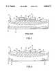
- the ESD protection device 16is formed by parallel NMOS transistors 22 and 24 located on the chip 12.
- the NMOS transistors 22 and 24are fabricated in a P-well 26 which is formed in an N-substrate 28.
- the transistors 22 and 24include sources 30a and 30b and gates 32a and 32b, respectively, as well as a common drain 34.
- a buried layer implant 36which forms a low current, low resistance path within the substrate 28.
- the buried layer implant 36extends throughout the entire substrate 28 of the CMOS IC below all active devices and components, including the ESD protection devices 16.
- a low-resistance buried layer implant 36inhibits the formation of parasitic bipolar transistors in all NMOS and PMOS transistors in all of the components of the CMOS device.
- the buried layer implant 36reduces the occurrence of latch-up within the device but, as the present invention recognizes, also inhibits the desired formation of parasitic bipolar transistors within the ESD protection device.
- the buried layer implant 36is absent beneath the ESD protection device 16.
- the absence of the buried layer implant 36 beneath the ESD protection device 16creates a relatively high resistance in the substrate 28 under the P-well 26 beneath the parallel transistors 22 and 24.
- a sufficiently high resistance in the substrate 28 below the NMOS transistors 22 and 24allows the pn junctions of the transistors 22 and 24 to become forward biased and parasitic bipolar transistors to be turned on more easily.
- the parasitic bipolar transistorsthen clamp the voltage at the drain 34 to a level below the breakdown voltage and shunt excess current away from the functional components 20 to ground.
- FIG. 4shows steps in forming the buried layer implant 36 within the substrate 28 of the CMOS IC 10, but not in an area 40 beneath each ESD protection device (not shown in FIG. 4).
- the area 40 on the substrate 28 upon which the ESD protection device will be formedis covered with a relatively thick layer of photoresist. (Not shown).
- the layer of photoresistis then patterned with typical photolythographic techniques and etched, leaving a mask 42.
- the mask 42 and the layer of photoresist from which it was patternedmust have physical properties sufficient to completely block the implant ions of the beam 38 (typically boron ions) from reaching the substrate 28 and from becoming implanted in the areas where the ESD protection devices will be formed. In many cases, a mask of approximately 6 micrometers is considered sufficient for blocking purposes.
- the buried layer 36is then formed by subjecting the entire substrate 28, including those areas 40 covered by the mask 42, to a high energy ion implantation beam 38.
- the ion beam 38implants a layer of ions throughout the substrate 28, creating a low resistance conductive region 36 everywhere except in those areas 40 covered by the mask 42.
- the mask 42is then removed and ESD protection devices are formed on the substrate 28 in those areas 40 formerly covered by the mask.
- the depth of the buried layer 36, as well as the concentration of the ions within the buried layer 36,is a function of the method and energy of the beam 38 used to implant the ions.
- Utilizing the ion beam masking method of the present inventionallows for the manufacture of a CMOS devices that simultaneously achieve improved latch-up performance and a lower snap-back voltage in the ESD protection device.
Landscapes
- Semiconductor Integrated Circuits (AREA)
- Metal-Oxide And Bipolar Metal-Oxide Semiconductor Integrated Circuits (AREA)
Abstract
Description
Claims (11)
Priority Applications (1)
| Application Number | Priority Date | Filing Date | Title |
|---|---|---|---|
| US09/245,193US6063672A (en) | 1999-02-05 | 1999-02-05 | NMOS electrostatic discharge protection device and method for CMOS integrated circuit |
Applications Claiming Priority (1)
| Application Number | Priority Date | Filing Date | Title |
|---|---|---|---|
| US09/245,193US6063672A (en) | 1999-02-05 | 1999-02-05 | NMOS electrostatic discharge protection device and method for CMOS integrated circuit |
Publications (1)
| Publication Number | Publication Date |
|---|---|
| US6063672Atrue US6063672A (en) | 2000-05-16 |
Family
ID=22925682
Family Applications (1)
| Application Number | Title | Priority Date | Filing Date |
|---|---|---|---|
| US09/245,193Expired - LifetimeUS6063672A (en) | 1999-02-05 | 1999-02-05 | NMOS electrostatic discharge protection device and method for CMOS integrated circuit |
Country Status (1)
| Country | Link |
|---|---|
| US (1) | US6063672A (en) |
Cited By (11)
| Publication number | Priority date | Publication date | Assignee | Title |
|---|---|---|---|---|
| US6281530B1 (en)* | 1998-11-05 | 2001-08-28 | Texas Instruments Incorporated | LPNP utilizing base ballast resistor |
| US20030085429A1 (en)* | 2001-11-02 | 2003-05-08 | Hulfachor Ronald B. | Triggering of an ESD NMOS through the use of an N-type buried layer |
| US6800516B2 (en) | 2003-01-21 | 2004-10-05 | Taiwan Semiconductor Manufacturing Company, Ltd. | Electrostatic discharge device protection structure |
| US20050179093A1 (en)* | 2004-02-17 | 2005-08-18 | Silicon Space Technology Corporation | Buried guard ring and radiation hardened isolation structures and fabrication methods |
| US20060259892A1 (en)* | 2005-05-11 | 2006-11-16 | Lsi Logic Corporation | R-cells containing CDM clamps |
| US20070141794A1 (en)* | 2005-10-14 | 2007-06-21 | Silicon Space Technology Corporation | Radiation hardened isolation structures and fabrication methods |
| US20080142899A1 (en)* | 2006-08-04 | 2008-06-19 | Silicon Space Technology Corporation | Radiation immunity of integrated circuits using backside die contact and electrically conductive layers |
| US7718480B1 (en)* | 2005-05-26 | 2010-05-18 | National Semiconductor Corporation | ESD clamps and NMOS arrays with increased electrical overstress robustness |
| US10038058B2 (en) | 2016-05-07 | 2018-07-31 | Silicon Space Technology Corporation | FinFET device structure and method for forming same |
| US20180247929A1 (en)* | 2017-02-25 | 2018-08-30 | Indian Institute Of Science | Semiconductor devices and methods to enhance electrostatic discharge (esd) robustness, latch-up, and hot carrier immunity |
| US20200066723A1 (en)* | 2018-08-24 | 2020-02-27 | Samsung Electro-Mechanics Co., Ltd. | Layout structure of cmos transistor with improved insertion loss |
Citations (26)
| Publication number | Priority date | Publication date | Assignee | Title |
|---|---|---|---|---|
| US4400711A (en)* | 1981-03-31 | 1983-08-23 | Rca Corporation | Integrated circuit protection device |
| JPS58162067A (en)* | 1982-03-23 | 1983-09-26 | Nec Corp | Manufacture of insulated gate field effect transistor |
| US4470191A (en)* | 1982-12-09 | 1984-09-11 | International Business Machines Corporation | Process for making complementary transistors by sequential implantations using oxidation barrier masking layer |
| JPH02184802A (en)* | 1989-01-11 | 1990-07-19 | Fuji Photo Film Co Ltd | Color separation filter |
| US4972247A (en)* | 1985-10-28 | 1990-11-20 | Silicon Systems, Inc. | High energy event protection for semiconductor devices |
| JPH0536909A (en)* | 1991-07-29 | 1993-02-12 | Nec Corp | Semiconductor integrated circuit |
| US5262344A (en)* | 1990-04-27 | 1993-11-16 | Digital Equipment Corporation | N-channel clamp for ESD protection in self-aligned silicided CMOS process |
| US5416351A (en)* | 1991-10-30 | 1995-05-16 | Harris Corporation | Electrostatic discharge protection |
| US5440163A (en)* | 1992-09-01 | 1995-08-08 | Nec Corporation | CMOS ESD protection structure |
| US5504362A (en)* | 1992-12-22 | 1996-04-02 | International Business Machines Corporation | Electrostatic discharge protection device |
| US5517049A (en)* | 1994-09-30 | 1996-05-14 | Vlsi Technology, Inc. | CMOS output buffer with enhanced ESD resistance |
| US5535086A (en)* | 1994-09-22 | 1996-07-09 | National Semiconductor Corp. | ESD protection circuit and method for BICMOS devices |
| US5545572A (en)* | 1993-10-21 | 1996-08-13 | Hyundai Electronics Industries Co., Ltd. | Method for fabricating electrostatic discharge protecting transistor |
| US5572394A (en)* | 1995-04-06 | 1996-11-05 | Industrial Technology Research Institute | CMOS on-chip four-LVTSCR ESD protection scheme |
| US5589415A (en)* | 1995-06-07 | 1996-12-31 | Sgs-Thomson Microelectronics, Inc. | Method for forming a semiconductor structure with self-aligned contacts |
| US5620920A (en)* | 1995-03-24 | 1997-04-15 | Deutsche Itt Industries Gmbh | Process for fabricating a CMOS structure with ESD protection |
| US5631793A (en)* | 1995-09-05 | 1997-05-20 | Winbond Electronics Corporation | Capacitor-couple electrostatic discharge protection circuit |
| US5637900A (en)* | 1995-04-06 | 1997-06-10 | Industrial Technology Research Institute | Latchup-free fully-protected CMOS on-chip ESD protection circuit |
| US5734186A (en)* | 1996-09-16 | 1998-03-31 | Delco Electronics Corporation | CMOS voltage clamp |
| US5814538A (en)* | 1996-03-19 | 1998-09-29 | Samsung Electronics Co., Ltd. | Methods of forming BiCMOS devices having dual-layer emitter electrodes and thin-film transistors therein |
| US5814866A (en)* | 1994-11-22 | 1998-09-29 | Genus, Inc. | Semiconductor device having at least one field oxide area and CMOS vertically modulated wells (VMW) with a buried implanted layer for lateral isolation having a first portion below a well, a second portion forming another, adjacent well, and a vertical po |
| US5838033A (en)* | 1993-09-08 | 1998-11-17 | Lucent Technologies Inc. | Integrated circuit with gate conductor defined resistor |
| US5841169A (en)* | 1996-06-27 | 1998-11-24 | Harris Corporation | Integrated circuit containing devices dielectrically isolated and junction isolated from a substrate |
| US5891792A (en)* | 1998-08-14 | 1999-04-06 | Taiwan Semiconductor Manufacturing Company, Ltd. | ESD device protection structure and process with high tilt angle GE implant |
| US5918127A (en)* | 1996-05-20 | 1999-06-29 | United Microelectronics Corp. | Method of enhancing electrostatic discharge (ESD) protection capability in integrated circuits |
| US5982003A (en)* | 1994-04-07 | 1999-11-09 | The Regents Of The University Of California | Silicon-on-insulator transistors having improved current characteristics and reduced electrostatic discharge susceptibility |
- 1999
- 1999-02-05USUS09/245,193patent/US6063672A/ennot_activeExpired - Lifetime
Patent Citations (27)
| Publication number | Priority date | Publication date | Assignee | Title |
|---|---|---|---|---|
| US4400711A (en)* | 1981-03-31 | 1983-08-23 | Rca Corporation | Integrated circuit protection device |
| JPS58162067A (en)* | 1982-03-23 | 1983-09-26 | Nec Corp | Manufacture of insulated gate field effect transistor |
| US4470191A (en)* | 1982-12-09 | 1984-09-11 | International Business Machines Corporation | Process for making complementary transistors by sequential implantations using oxidation barrier masking layer |
| US4972247A (en)* | 1985-10-28 | 1990-11-20 | Silicon Systems, Inc. | High energy event protection for semiconductor devices |
| JPH02184802A (en)* | 1989-01-11 | 1990-07-19 | Fuji Photo Film Co Ltd | Color separation filter |
| US5262344A (en)* | 1990-04-27 | 1993-11-16 | Digital Equipment Corporation | N-channel clamp for ESD protection in self-aligned silicided CMOS process |
| JPH0536909A (en)* | 1991-07-29 | 1993-02-12 | Nec Corp | Semiconductor integrated circuit |
| US5416351A (en)* | 1991-10-30 | 1995-05-16 | Harris Corporation | Electrostatic discharge protection |
| US5440163A (en)* | 1992-09-01 | 1995-08-08 | Nec Corporation | CMOS ESD protection structure |
| US5504362A (en)* | 1992-12-22 | 1996-04-02 | International Business Machines Corporation | Electrostatic discharge protection device |
| US5838033A (en)* | 1993-09-08 | 1998-11-17 | Lucent Technologies Inc. | Integrated circuit with gate conductor defined resistor |
| US5545572A (en)* | 1993-10-21 | 1996-08-13 | Hyundai Electronics Industries Co., Ltd. | Method for fabricating electrostatic discharge protecting transistor |
| US5907174A (en)* | 1993-10-21 | 1999-05-25 | Hyundai Electronics Industries Co., Ltd. | Electrostatic discharge protecting transistor |
| US5982003A (en)* | 1994-04-07 | 1999-11-09 | The Regents Of The University Of California | Silicon-on-insulator transistors having improved current characteristics and reduced electrostatic discharge susceptibility |
| US5535086A (en)* | 1994-09-22 | 1996-07-09 | National Semiconductor Corp. | ESD protection circuit and method for BICMOS devices |
| US5517049A (en)* | 1994-09-30 | 1996-05-14 | Vlsi Technology, Inc. | CMOS output buffer with enhanced ESD resistance |
| US5814866A (en)* | 1994-11-22 | 1998-09-29 | Genus, Inc. | Semiconductor device having at least one field oxide area and CMOS vertically modulated wells (VMW) with a buried implanted layer for lateral isolation having a first portion below a well, a second portion forming another, adjacent well, and a vertical po |
| US5620920A (en)* | 1995-03-24 | 1997-04-15 | Deutsche Itt Industries Gmbh | Process for fabricating a CMOS structure with ESD protection |
| US5637900A (en)* | 1995-04-06 | 1997-06-10 | Industrial Technology Research Institute | Latchup-free fully-protected CMOS on-chip ESD protection circuit |
| US5572394A (en)* | 1995-04-06 | 1996-11-05 | Industrial Technology Research Institute | CMOS on-chip four-LVTSCR ESD protection scheme |
| US5589415A (en)* | 1995-06-07 | 1996-12-31 | Sgs-Thomson Microelectronics, Inc. | Method for forming a semiconductor structure with self-aligned contacts |
| US5631793A (en)* | 1995-09-05 | 1997-05-20 | Winbond Electronics Corporation | Capacitor-couple electrostatic discharge protection circuit |
| US5814538A (en)* | 1996-03-19 | 1998-09-29 | Samsung Electronics Co., Ltd. | Methods of forming BiCMOS devices having dual-layer emitter electrodes and thin-film transistors therein |
| US5918127A (en)* | 1996-05-20 | 1999-06-29 | United Microelectronics Corp. | Method of enhancing electrostatic discharge (ESD) protection capability in integrated circuits |
| US5841169A (en)* | 1996-06-27 | 1998-11-24 | Harris Corporation | Integrated circuit containing devices dielectrically isolated and junction isolated from a substrate |
| US5734186A (en)* | 1996-09-16 | 1998-03-31 | Delco Electronics Corporation | CMOS voltage clamp |
| US5891792A (en)* | 1998-08-14 | 1999-04-06 | Taiwan Semiconductor Manufacturing Company, Ltd. | ESD device protection structure and process with high tilt angle GE implant |
Cited By (31)
| Publication number | Priority date | Publication date | Assignee | Title |
|---|---|---|---|---|
| US6281530B1 (en)* | 1998-11-05 | 2001-08-28 | Texas Instruments Incorporated | LPNP utilizing base ballast resistor |
| US20030085429A1 (en)* | 2001-11-02 | 2003-05-08 | Hulfachor Ronald B. | Triggering of an ESD NMOS through the use of an N-type buried layer |
| WO2003096418A1 (en)* | 2001-11-02 | 2003-11-20 | Fairchild Semiconductor Corporation | Improving the triggering of an esd nmos through the use of an n-type buried layer |
| US6855964B2 (en) | 2001-11-02 | 2005-02-15 | Farichild Semiconductor Corporation | Triggering of an ESD NMOS through the use of an N-type buried layer |
| KR100954471B1 (en) | 2001-11-02 | 2010-04-22 | 페어차일드 세미컨덕터 코포레이션 | ESD NMOS devices and formation methods, and systems including the same |
| CN100347855C (en)* | 2001-11-02 | 2007-11-07 | 快捷半导体有限公司 | Triggering of an ESD NMOS through the use of an n-type buried layer |
| US6800516B2 (en) | 2003-01-21 | 2004-10-05 | Taiwan Semiconductor Manufacturing Company, Ltd. | Electrostatic discharge device protection structure |
| US8729640B2 (en) | 2004-02-17 | 2014-05-20 | Silicon Space Technology Corporation | Method and structure for radiation hardening a semiconductor device |
| US7804138B2 (en) | 2004-02-17 | 2010-09-28 | Silicon Space Technology Corp. | Buried guard ring and radiation hardened isolation structures and fabrication methods |
| US8497195B2 (en) | 2004-02-17 | 2013-07-30 | Silicon Space Technology Corporation | Method for radiation hardening a semiconductor device |
| US20060249759A1 (en)* | 2004-02-17 | 2006-11-09 | Morris Wesley H | Buried guard ring and radiation hardened isolation structures and fabrication methods |
| US7304354B2 (en) | 2004-02-17 | 2007-12-04 | Silicon Space Technology Corp. | Buried guard ring and radiation hardened isolation structures and fabrication methods |
| US20080073725A1 (en)* | 2004-02-17 | 2008-03-27 | Morris Wesley H | Buried guard ring structures and fabrication methods |
| US8093145B2 (en) | 2004-02-17 | 2012-01-10 | Silicon Space Technology Corp. | Methods for operating and fabricating a semiconductor device having a buried guard ring structure |
| US20080188045A1 (en)* | 2004-02-17 | 2008-08-07 | Morris Wesley H | Methods for operating and fabricating a semiconductor device having a buried guard ring structure |
| US7629654B2 (en) | 2004-02-17 | 2009-12-08 | Silicon Space Technology Corp. | Buried guard ring structures and fabrication methods |
| US20050179093A1 (en)* | 2004-02-17 | 2005-08-18 | Silicon Space Technology Corporation | Buried guard ring and radiation hardened isolation structures and fabrication methods |
| US20060259892A1 (en)* | 2005-05-11 | 2006-11-16 | Lsi Logic Corporation | R-cells containing CDM clamps |
| US7272802B2 (en)* | 2005-05-11 | 2007-09-18 | Lsi Corporation | R-cells containing CDM clamps |
| US7718480B1 (en)* | 2005-05-26 | 2010-05-18 | National Semiconductor Corporation | ESD clamps and NMOS arrays with increased electrical overstress robustness |
| US20070141794A1 (en)* | 2005-10-14 | 2007-06-21 | Silicon Space Technology Corporation | Radiation hardened isolation structures and fabrication methods |
| US8252642B2 (en) | 2005-10-14 | 2012-08-28 | Silicon Space Technology Corp. | Fabrication methods for radiation hardened isolation structures |
| US8278719B2 (en) | 2005-10-14 | 2012-10-02 | Silicon Space Technology Corp. | Radiation hardened isolation structures and fabrication methods |
| US20100267212A1 (en)* | 2005-10-14 | 2010-10-21 | Morris Wesley H | Fabrication methods for radiation hardened isolation structures |
| US20080142899A1 (en)* | 2006-08-04 | 2008-06-19 | Silicon Space Technology Corporation | Radiation immunity of integrated circuits using backside die contact and electrically conductive layers |
| US10038058B2 (en) | 2016-05-07 | 2018-07-31 | Silicon Space Technology Corporation | FinFET device structure and method for forming same |
| US10615260B1 (en) | 2016-05-07 | 2020-04-07 | Silicon Space Technology Corporation | Method for forming FinFET device structure |
| US20180247929A1 (en)* | 2017-02-25 | 2018-08-30 | Indian Institute Of Science | Semiconductor devices and methods to enhance electrostatic discharge (esd) robustness, latch-up, and hot carrier immunity |
| US10483258B2 (en)* | 2017-02-25 | 2019-11-19 | Indian Institute Of Science | Semiconductor devices and methods to enhance electrostatic discharge (ESD) robustness, latch-up, and hot carrier immunity |
| US20200066723A1 (en)* | 2018-08-24 | 2020-02-27 | Samsung Electro-Mechanics Co., Ltd. | Layout structure of cmos transistor with improved insertion loss |
| US10868010B2 (en)* | 2018-08-24 | 2020-12-15 | Samsung Electro-Mechanics Co., Ltd. | Layout structure of CMOS transistor with improved insertion loss |
Similar Documents
| Publication | Publication Date | Title |
|---|---|---|
| US7429774B2 (en) | Electrostatic discharge (ESD) protection MOS device and ESD circuitry thereof | |
| US5272371A (en) | Electrostatic discharge protection structure | |
| US5728612A (en) | Method for forming minimum area structures for sub-micron CMOS ESD protection in integrated circuit structures without extra implant and mask steps, and articles formed thereby | |
| US7372083B2 (en) | Embedded silicon-controlled rectifier (SCR) for HVPMOS ESD protection | |
| US7384802B2 (en) | ESD protection device for high voltage | |
| US7709896B2 (en) | ESD protection device and method | |
| US6420761B1 (en) | Asymmetrical semiconductor device for ESD protection | |
| US5883414A (en) | Electrostatic discharge protection device | |
| JPH06196634A (en) | Depletion control type separation stage | |
| US7462885B2 (en) | ESD structure for high voltage ESD protection | |
| JPH10256393A (en) | Semiconductor device | |
| US6767810B2 (en) | Method to increase substrate potential in MOS transistors used in ESD protection circuits | |
| US6063672A (en) | NMOS electrostatic discharge protection device and method for CMOS integrated circuit | |
| US6323522B1 (en) | Silicon on insulator thick oxide structure and process of manufacture | |
| JP2002324847A (en) | Semiconductor device and manufacturing method thereof | |
| US7202527B2 (en) | MOS transistor and ESD protective device each having a settable voltage ratio of the lateral breakdown voltage to the vertical breakdown voltage | |
| US7955923B1 (en) | I/O ESD protection device for high performance circuits | |
| US5607867A (en) | Method of forming a controlled low collector breakdown voltage transistor for ESD protection circuits | |
| US6169001B1 (en) | CMOS device with deep current path for ESD protection | |
| KR100504203B1 (en) | Protecting device of semiconductor device | |
| US5539233A (en) | Controlled low collector breakdown voltage vertical transistor for ESD protection circuits | |
| CN111725206A (en) | SCR device triggered by PMOS, manufacturing method of SCR device and SCR electrostatic protection circuit | |
| US6225662B1 (en) | Semiconductor structure with heavily doped buried breakdown region | |
| US6987301B1 (en) | Electrostatic discharge protection | |
| KR19980041852A (en) | A ground-gate transistor having a reduced breakdown voltage |
Legal Events
| Date | Code | Title | Description |
|---|---|---|---|
| AS | Assignment | Owner name:LSI LOGIC CORPORATION, CALIFORNIA Free format text:ASSIGNMENT OF ASSIGNORS INTEREST;ASSIGNORS:MILLER, GAYLE W.;GIOIA, SAMUEL C.;RANDAZZO, TODD A.;REEL/FRAME:009933/0323;SIGNING DATES FROM 19990406 TO 19990422 | |
| STCF | Information on status: patent grant | Free format text:PATENTED CASE | |
| FPAY | Fee payment | Year of fee payment:4 | |
| FPAY | Fee payment | Year of fee payment:8 | |
| FEPP | Fee payment procedure | Free format text:PAYOR NUMBER ASSIGNED (ORIGINAL EVENT CODE: ASPN); ENTITY STATUS OF PATENT OWNER: LARGE ENTITY Free format text:PAYER NUMBER DE-ASSIGNED (ORIGINAL EVENT CODE: RMPN); ENTITY STATUS OF PATENT OWNER: LARGE ENTITY | |
| FPAY | Fee payment | Year of fee payment:12 | |
| AS | Assignment | Owner name:DEUTSCHE BANK AG NEW YORK BRANCH, AS COLLATERAL AG Free format text:PATENT SECURITY AGREEMENT;ASSIGNORS:LSI CORPORATION;AGERE SYSTEMS LLC;REEL/FRAME:032856/0031 Effective date:20140506 | |
| AS | Assignment | Owner name:LSI CORPORATION, CALIFORNIA Free format text:CHANGE OF NAME;ASSIGNOR:LSI LOGIC CORPORATION;REEL/FRAME:033102/0270 Effective date:20070406 | |
| AS | Assignment | Owner name:AVAGO TECHNOLOGIES GENERAL IP (SINGAPORE) PTE. LTD Free format text:ASSIGNMENT OF ASSIGNORS INTEREST;ASSIGNOR:LSI CORPORATION;REEL/FRAME:035390/0388 Effective date:20140814 | |
| AS | Assignment | Owner name:AGERE SYSTEMS LLC, PENNSYLVANIA Free format text:TERMINATION AND RELEASE OF SECURITY INTEREST IN PATENT RIGHTS (RELEASES RF 032856-0031);ASSIGNOR:DEUTSCHE BANK AG NEW YORK BRANCH, AS COLLATERAL AGENT;REEL/FRAME:037684/0039 Effective date:20160201 Owner name:LSI CORPORATION, CALIFORNIA Free format text:TERMINATION AND RELEASE OF SECURITY INTEREST IN PATENT RIGHTS (RELEASES RF 032856-0031);ASSIGNOR:DEUTSCHE BANK AG NEW YORK BRANCH, AS COLLATERAL AGENT;REEL/FRAME:037684/0039 Effective date:20160201 | |
| AS | Assignment | Owner name:BANK OF AMERICA, N.A., AS COLLATERAL AGENT, NORTH CAROLINA Free format text:PATENT SECURITY AGREEMENT;ASSIGNOR:AVAGO TECHNOLOGIES GENERAL IP (SINGAPORE) PTE. LTD.;REEL/FRAME:037808/0001 Effective date:20160201 Owner name:BANK OF AMERICA, N.A., AS COLLATERAL AGENT, NORTH Free format text:PATENT SECURITY AGREEMENT;ASSIGNOR:AVAGO TECHNOLOGIES GENERAL IP (SINGAPORE) PTE. LTD.;REEL/FRAME:037808/0001 Effective date:20160201 | |
| AS | Assignment | Owner name:AVAGO TECHNOLOGIES GENERAL IP (SINGAPORE) PTE. LTD., SINGAPORE Free format text:TERMINATION AND RELEASE OF SECURITY INTEREST IN PATENTS;ASSIGNOR:BANK OF AMERICA, N.A., AS COLLATERAL AGENT;REEL/FRAME:041710/0001 Effective date:20170119 Owner name:AVAGO TECHNOLOGIES GENERAL IP (SINGAPORE) PTE. LTD Free format text:TERMINATION AND RELEASE OF SECURITY INTEREST IN PATENTS;ASSIGNOR:BANK OF AMERICA, N.A., AS COLLATERAL AGENT;REEL/FRAME:041710/0001 Effective date:20170119 | |
| AS | Assignment | Owner name:BELL SEMICONDUCTOR, LLC, ILLINOIS Free format text:ASSIGNMENT OF ASSIGNORS INTEREST;ASSIGNORS:AVAGO TECHNOLOGIES GENERAL IP (SINGAPORE) PTE. LTD.;BROADCOM CORPORATION;REEL/FRAME:044886/0001 Effective date:20171208 | |
| AS | Assignment | Owner name:CORTLAND CAPITAL MARKET SERVICES LLC, AS COLLATERA Free format text:SECURITY INTEREST;ASSIGNORS:HILCO PATENT ACQUISITION 56, LLC;BELL SEMICONDUCTOR, LLC;BELL NORTHERN RESEARCH, LLC;REEL/FRAME:045216/0020 Effective date:20180124 | |
| AS | Assignment | Owner name:BELL NORTHERN RESEARCH, LLC, ILLINOIS Free format text:SECURITY INTEREST;ASSIGNOR:CORTLAND CAPITAL MARKET SERVICES LLC;REEL/FRAME:060885/0001 Effective date:20220401 Owner name:BELL SEMICONDUCTOR, LLC, ILLINOIS Free format text:SECURITY INTEREST;ASSIGNOR:CORTLAND CAPITAL MARKET SERVICES LLC;REEL/FRAME:060885/0001 Effective date:20220401 Owner name:HILCO PATENT ACQUISITION 56, LLC, ILLINOIS Free format text:SECURITY INTEREST;ASSIGNOR:CORTLAND CAPITAL MARKET SERVICES LLC;REEL/FRAME:060885/0001 Effective date:20220401 |