US6061242A - Die paddle heat sink with thermal posts - Google Patents
Die paddle heat sink with thermal postsDownload PDFInfo
- Publication number
- US6061242A US6061242AUS09/257,567US25756799AUS6061242AUS 6061242 AUS6061242 AUS 6061242AUS 25756799 AUS25756799 AUS 25756799AUS 6061242 AUS6061242 AUS 6061242A
- Authority
- US
- United States
- Prior art keywords
- die paddle
- die
- recited
- semiconductor device
- semiconductor
- Prior art date
- Legal status (The legal status is an assumption and is not a legal conclusion. Google has not performed a legal analysis and makes no representation as to the accuracy of the status listed.)
- Expired - Lifetime
Links
- 239000004065semiconductorSubstances0.000claimsabstractdescription142
- 230000017525heat dissipationEffects0.000claimsabstractdescription16
- 238000000034methodMethods0.000claimsdescription25
- 238000001816coolingMethods0.000claimsdescription6
- 239000004020conductorSubstances0.000claimsdescription5
- 238000005530etchingMethods0.000claims1
- 238000000465mouldingMethods0.000claims1
- 239000000463materialSubstances0.000description7
- 241000237858GastropodaSpecies0.000description2
- 239000007788liquidSubstances0.000description2
- 239000002184metalSubstances0.000description2
- 239000012811non-conductive materialSubstances0.000description2
- 238000004806packaging method and processMethods0.000description2
- 229910000679solderInorganic materials0.000description2
- 230000008878couplingEffects0.000description1
- 238000010168coupling processMethods0.000description1
- 238000005859coupling reactionMethods0.000description1
- 238000005336crackingMethods0.000description1
- 238000000354decomposition reactionMethods0.000description1
- 230000003467diminishing effectEffects0.000description1
- 238000004519manufacturing processMethods0.000description1
- 239000005022packaging materialSubstances0.000description1
- 230000002459sustained effectEffects0.000description1
Images


Classifications
- H—ELECTRICITY
- H05—ELECTRIC TECHNIQUES NOT OTHERWISE PROVIDED FOR
- H05K—PRINTED CIRCUITS; CASINGS OR CONSTRUCTIONAL DETAILS OF ELECTRIC APPARATUS; MANUFACTURE OF ASSEMBLAGES OF ELECTRICAL COMPONENTS
- H05K3/00—Apparatus or processes for manufacturing printed circuits
- H05K3/30—Assembling printed circuits with electric components, e.g. with resistor
- H05K3/303—Surface mounted components, e.g. affixing before soldering, aligning means, spacing means
- H—ELECTRICITY
- H01—ELECTRIC ELEMENTS
- H01L—SEMICONDUCTOR DEVICES NOT COVERED BY CLASS H10
- H01L23/00—Details of semiconductor or other solid state devices
- H01L23/48—Arrangements for conducting electric current to or from the solid state body in operation, e.g. leads, terminal arrangements ; Selection of materials therefor
- H01L23/488—Arrangements for conducting electric current to or from the solid state body in operation, e.g. leads, terminal arrangements ; Selection of materials therefor consisting of soldered or bonded constructions
- H01L23/495—Lead-frames or other flat leads
- H01L23/49568—Lead-frames or other flat leads specifically adapted to facilitate heat dissipation
- H—ELECTRICITY
- H01—ELECTRIC ELEMENTS
- H01L—SEMICONDUCTOR DEVICES NOT COVERED BY CLASS H10
- H01L2924/00—Indexing scheme for arrangements or methods for connecting or disconnecting semiconductor or solid-state bodies as covered by H01L24/00
- H01L2924/0001—Technical content checked by a classifier
- H01L2924/0002—Not covered by any one of groups H01L24/00, H01L24/00 and H01L2224/00
- H—ELECTRICITY
- H05—ELECTRIC TECHNIQUES NOT OTHERWISE PROVIDED FOR
- H05K—PRINTED CIRCUITS; CASINGS OR CONSTRUCTIONAL DETAILS OF ELECTRIC APPARATUS; MANUFACTURE OF ASSEMBLAGES OF ELECTRICAL COMPONENTS
- H05K2201/00—Indexing scheme relating to printed circuits covered by H05K1/00
- H05K2201/10—Details of components or other objects attached to or integrated in a printed circuit board
- H05K2201/10431—Details of mounted components
- H05K2201/10439—Position of a single component
- H05K2201/10454—Vertically mounted
- H—ELECTRICITY
- H05—ELECTRIC TECHNIQUES NOT OTHERWISE PROVIDED FOR
- H05K—PRINTED CIRCUITS; CASINGS OR CONSTRUCTIONAL DETAILS OF ELECTRIC APPARATUS; MANUFACTURE OF ASSEMBLAGES OF ELECTRICAL COMPONENTS
- H05K2201/00—Indexing scheme relating to printed circuits covered by H05K1/00
- H05K2201/10—Details of components or other objects attached to or integrated in a printed circuit board
- H05K2201/10613—Details of electrical connections of non-printed components, e.g. special leads
- H05K2201/10621—Components characterised by their electrical contacts
- H05K2201/10659—Different types of terminals for the same component, e.g. solder balls combined with leads
- H—ELECTRICITY
- H05—ELECTRIC TECHNIQUES NOT OTHERWISE PROVIDED FOR
- H05K—PRINTED CIRCUITS; CASINGS OR CONSTRUCTIONAL DETAILS OF ELECTRIC APPARATUS; MANUFACTURE OF ASSEMBLAGES OF ELECTRICAL COMPONENTS
- H05K2201/00—Indexing scheme relating to printed circuits covered by H05K1/00
- H05K2201/10—Details of components or other objects attached to or integrated in a printed circuit board
- H05K2201/10613—Details of electrical connections of non-printed components, e.g. special leads
- H05K2201/10621—Components characterised by their electrical contacts
- H05K2201/10696—Single-in-line [SIL] package
- H—ELECTRICITY
- H05—ELECTRIC TECHNIQUES NOT OTHERWISE PROVIDED FOR
- H05K—PRINTED CIRCUITS; CASINGS OR CONSTRUCTIONAL DETAILS OF ELECTRIC APPARATUS; MANUFACTURE OF ASSEMBLAGES OF ELECTRICAL COMPONENTS
- H05K2203/00—Indexing scheme relating to apparatus or processes for manufacturing printed circuits covered by H05K3/00
- H05K2203/16—Inspection; Monitoring; Aligning
- H05K2203/167—Using mechanical means for positioning, alignment or registration, e.g. using rod-in-hole alignment
- Y—GENERAL TAGGING OF NEW TECHNOLOGICAL DEVELOPMENTS; GENERAL TAGGING OF CROSS-SECTIONAL TECHNOLOGIES SPANNING OVER SEVERAL SECTIONS OF THE IPC; TECHNICAL SUBJECTS COVERED BY FORMER USPC CROSS-REFERENCE ART COLLECTIONS [XRACs] AND DIGESTS
- Y02—TECHNOLOGIES OR APPLICATIONS FOR MITIGATION OR ADAPTATION AGAINST CLIMATE CHANGE
- Y02P—CLIMATE CHANGE MITIGATION TECHNOLOGIES IN THE PRODUCTION OR PROCESSING OF GOODS
- Y02P70/00—Climate change mitigation technologies in the production process for final industrial or consumer products
- Y02P70/50—Manufacturing or production processes characterised by the final manufactured product
Definitions
- the present inventionrelates generally to semiconductor packaging mounting packages. More particularly, it pertains to heat dissipation for a semiconductor packaging mounting package.
- Integrated circuitsare being produced with diminishing geometries and increasing densities. Associated with the increase in density is an increase in the amount of heat generated by a semiconductor die per square unit of area, and also increased power consumption.
- Increased semiconductor device power consumption and increased densitytranslates into increased semiconductor device operating temperatures.
- Heat generated by a semiconductor devicemigrates through the plastic packaging material and can reach damaging temperatures, where sustained high operating temperatures can result in a decrease in performance of the semiconductor device or even semiconductor device failure.
- the high temperaturescan result in a process of decomposition resulting in package cracking and eventual device failure.
- a semiconductor device which is capable of dissipating heatincludes a die paddle including an integral heat dissipation device and a semiconductor die, which is thermally coupled with the die paddle.
- the semiconductor dieis coupled with the die paddle with a thermally conductive paste, a non-conductive paste, or double-sided tape, or other equivalent methods or materials.
- a package of plastic or other suitable materialencompasses at least a portion of, or optionally fully, the semiconductor die and the die paddle.
- the packageencompasses about 50% of the die paddle. In another embodiment, the package encompasses about 80% of the die paddle. In yet another embodiment, the package encompasses about 95% of the die paddle. Alternatively, the package encompasses about 50%-95% of the die paddle.
- the die paddlehas a front surface and a rear surface, and, in one embodiment, the semiconductor die is disposed on the front surface and the rear surface exposed to an environment. In another embodiment, the package encompasses side surfaces of the die paddle, and the rear surface is exposed to an environment.
- the die paddleis defined in part by a first surface area and the package is defined by a second surface area.
- the first surface area of the die paddleis maximized relative to the second surface area of the package.
- the semiconductorfurther includes thermal posts which extend from with the die paddle.
- the thermal postsare adapted for attaching and aligning the semiconductor device with a printed circuit board and assist in directing heat from the semiconductor device to a printed circuit board.
- the semiconductor deviceoptionally includes a lead electrically coupled with the semiconductor die, and the package encompasses a portion of the lead.
- the die paddlecomprises a ground plane.
- the semiconductor deviceallows for increased heat dissipation therefrom without requiring additional heat sinks or heat slugs to be attached thereto. This reduces the overall cost of the semiconductor device since fewer parts are required and assembly time is thereby reduced. Furthermore, cycle time to produce the semiconductor device can be reduced since fewer parts are assembled.
- Using the die paddle as the heat dissipatorprovides for improved thermal performance and package reliability. Having the die paddle partially exposed facilitates improved heat dissipation through convection.
- the electrical performance of the semiconductor deviceis increased by reducing the loop inductance.
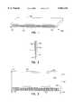
- FIG. 1is a perspective view illustrating a semiconductor device.
- FIG. 2is a side cut-away view illustrating a semiconductor device.
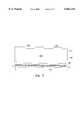
- FIG. 3is a front elevation illustrating the semiconductor device.
- FIG. 4is a front elevation illustrating a circuit board assembly.
- FIG. 5is a perspective view illustrating a semiconductor device.
- FIG. 5Ais a perspective view illustrating a semiconductor device.
- FIG. 5Bis a perspective view illustrating a semiconductor device.
- FIG. 6is a side cut-away view illustrating a semiconductor device.
- FIG. 6Ais a cut-away view illustrating a semiconductor device.
- FIG. 7is rear elevation illustrating a circuit board assembly.
- FIGS. 1 and 2illustrate a first embodiment of a semiconductor device 100.
- the semiconductor deviceincludes a die paddle 110 a semiconductor die 120, and a package body 130.
- the semiconductor device 100further includes a plurality of vertical surface mount gull-wing zig-zag package leads 112 extending therefrom.
- the leads 112extend from the die paddle 110 as will be further described below.
- the semiconductor die 120includes circuitry formed thereon.
- the semiconductor die 120is attached to the die paddle 110 for example, by conductive paste.
- the semiconductor die 120can be attached to the die paddle 110 using other methods or materials such as non-conductive paste or double sided tape.
- a pocketcan be etched on the die paddle 110.
- the die paddle 110is defined by a front surface 115, a rear surface 116, side surfaces 117, a top surface 118, and a bottom surface 119.
- the semiconductor side 120is coupled with the front surface 115 of the die paddle 110 by methods or materials, as mentioned above.
- the die paddle 110is coupled with a printed circuit board 180, where the bottom surface 119 is disposed proximate to the printed circuit board 180, as shown in FIG. 4.
- the die paddle 110includes leads 112 extending therefrom.
- the leads 112extend out through the package body 130 and can be formed to accommodate a variety of mounting styles.
- the leads 112allow for the electrical connection between the semiconductor device 100 and for instance, a printed circuit board 180, as shown in FIG. 4.
- the die paddle 110further includes thermal posts 114 extending therefrom, and are adapted to attach to a printed circuit board 180.
- the thermal posts 114provide a thermal path from the die paddle 110 and the semiconductor device 100 to the printed circuit board 180, which directs heat away from the semiconductor device 100.
- the thermal posts 114further provide alignment of the semiconductor device 100 while it is being installed on the printed circuit board 180.
- the thermal posts 114further allow for mechanical support during placement of the semiconductor device 100 on the printed circuit board 180 and during the solder reflow operation, where the leads 112 are connected with the printed circuit board 180.
- the thermal posts 114are connected to a ground on a printed circuit board, which allows for the die paddle 110 to serve as a ground.
- the semiconductor device 100further includes a package body 130, which completely encapsulates the die paddle 110 and the semiconductor die 120.
- the leads 112 and the thermal posts 114extend outside of the package body 130 so as to allow connection with the printed circuit board 180.
- the package body 130is formed of plastic. Alternatively, other electrically non-conductive materials can be used as well.
- the package body 130in one embodiment, is molded over the die paddle 110, thereby encapsulating the die paddle 110.
- the package body 130protects the semiconductor die 120 from the surrounding environment, and seals the die 120 therein. However, the package body 130 does not efficiently dissipate heat from the semiconductor device 100.
- the die paddle 110is increased in size relative to the package body 130 to serve as a heat dissipation device.
- the die paddlehas substantially the same size as the package body 130.
- the heat dissipation devicewhich is directly and thermally coupled with the semiconductor die 120 and the printed circuit board 180 allows for heat to be more efficiently dissipated from the semiconductor device 100.
- the die paddle 110is formed of a metal, which is a thermally conductive material.
- the die paddle 110can be formed, for example, by stamping.
- FIGS. 5-7illustrate another embodiment of a semiconductor device 200.
- the semiconductor deviceincludes a die paddle 210, a semiconductor die 220, and a package body 230.
- the semiconductor device 200further includes a plurality of vertical surface mount gull-wing zig-zag package leads 212 extending therefrom.
- the leads 212extend from the die paddle 210 as will be further described below.
- the semiconductor die 220includes circuitry formed thereon.
- the semiconductor die 220is attached to the die paddle 210 for example, by conductive paste.
- the semiconductor die 220can be attached to the die paddle 210 using other methods or materials such as non-conductive paste or double sided tape.
- a pocket 211(FIG. 6A) can be etched on the die paddle 210.
- the semiconductor die 220is mounted to the die paddle 210 using leads over chip (LOC) methods, as is known in the art. Wire bonding or an equivalent is used to connect selected bond pads on the die 220 to selected leads 212 or conductors of a lead frame.
- LOCleads over chip
- the die paddle 210is defined by a front surface 215, a rear surface 216, side surfaces 217, a top surface 218, and a bottom surface 219.
- the semiconductor side 220is coupled with the front surface 215 of the die paddle 210 by methods or materials, as mentioned above.
- the die paddle 210is coupled with a printed circuit board 280, where the bottom surface 219 is disposed proximate to the printed circuit board 280, as shown in FIG. 7.
- the die paddle 210includes leads 212 extending therefrom.
- the leads 212extend out through the package body 230 and can be formed to accommodate a variety of mounting styles.
- the leads 212allow for the electrical connection between the semiconductor device 200 and for instance, a printed circuit board 280, as shown in FIG. 7.
- the die paddle 210further includes thermal posts 214 extending therefrom, and are adapted to attach to a printed circuit board 280.
- the thermal posts 214provide a thermal path from the die paddle 210 and the semiconductor device 200 to the printed circuit board 280, which directs heat away from the semiconductor device 200.
- the thermal posts 214further provide alignment of the semiconductor device 200 while it is being installed on the printed circuit board 280.
- the thermal posts 214further allow for mechanical support during placement of the semiconductor device 200 on the printed circuit board 280 and during the solder reflow operation, where the leads 212 are connected with the printed circuit board 280.
- the semiconductor device 200further includes a package body 230, which in one embodiment, at least partially encapsulates the die paddle 210 and the semiconductor die 220, where the rear surface 216 of the die paddle 210 is partially or fully exposed to the environment.
- the front surface 215, on which the semiconductor die 220 is disposed,is encapsulated by the package body 230.
- the side surfaces 217 of the die paddle 210are encompassed by the package body 230.
- the package body 230encompasses at least 50% of the die paddle 210 (FIG. 5A).
- the package body 230in another embodiment, encompasses at least 80% of the die paddle 210 (FIG. 5). In yet another embodiment, the die paddle 210 is encompassed at least 95% by the package body 230 (FIG. 5B). Alternatively, the die paddle 210 is encompassed between 50% and 95% by the package body. Having the die paddle 210 partially exposed to the environment aids in the dissipation of heat, and the semiconductor die 220 is protected from the environment. Heat dissipation can be further facilitated by drawing air, or another medium, over the exposed surface of the die paddle 210.
- the leads 212 and the thermal posts 214extend outside of the package body 230 so as to allow connection with the printed circuit board 280.
- the package body 230is formed of plastic. Alternatively, other electrically non-conductive materials can be used as well.
- the package body 230in one embodiment, is molded over the die paddle 210, thereby encapsulating the die paddle 210.
- the package body 230protects the semiconductor die 220 from the surrounding environment, and seals the die 220 therein. However, the package body 230 does not efficiently dissipate heat from the semiconductor device 200.
- the die paddle 210is increased in size relative to the package body 230 to serve as a heat dissipation device.
- the die paddlehas substantially the same size as the package body 230.
- the heat dissipation devicewhich is directly and thermally coupled with the semiconductor die 220 and the printed circuit board 280 allows for heat to be more efficiently dissipated from the semiconductor device 200.
- the die paddle 210is formed of a metal, which is a thermally conductive material.
- the die paddle 210can be formed, for example, by stamping or other equivalent methods.
- the semiconductor deviceallows for increased heat dissipation therefrom without requiring additional heat sinks or heat slugs to be attached thereto. This reduces the overall cost of the semiconductor device since fewer parts are required and assembly time is thereby reduced. Furthermore, cycle time to produce the semiconductor device can be reduced since fewer parts are assembled.
- Using the die paddle as the heat dissipatorprovides for improved thermal performance and package reliability. Having the die paddle partially exposed facilitates improved heat dissipation through convection.
- the electrical performance of the semiconductor deviceis increased by reducing the loop inductance.
Landscapes
- Engineering & Computer Science (AREA)
- Microelectronics & Electronic Packaging (AREA)
- Physics & Mathematics (AREA)
- Condensed Matter Physics & Semiconductors (AREA)
- General Physics & Mathematics (AREA)
- Computer Hardware Design (AREA)
- Power Engineering (AREA)
- Manufacturing & Machinery (AREA)
- Cooling Or The Like Of Semiconductors Or Solid State Devices (AREA)
Abstract
Description
Claims (50)
Priority Applications (1)
| Application Number | Priority Date | Filing Date | Title |
|---|---|---|---|
| US09/257,567US6061242A (en) | 1999-02-25 | 1999-02-25 | Die paddle heat sink with thermal posts |
Applications Claiming Priority (1)
| Application Number | Priority Date | Filing Date | Title |
|---|---|---|---|
| US09/257,567US6061242A (en) | 1999-02-25 | 1999-02-25 | Die paddle heat sink with thermal posts |
Publications (1)
| Publication Number | Publication Date |
|---|---|
| US6061242Atrue US6061242A (en) | 2000-05-09 |
Family
ID=22976814
Family Applications (1)
| Application Number | Title | Priority Date | Filing Date |
|---|---|---|---|
| US09/257,567Expired - LifetimeUS6061242A (en) | 1999-02-25 | 1999-02-25 | Die paddle heat sink with thermal posts |
Country Status (1)
| Country | Link |
|---|---|
| US (1) | US6061242A (en) |
Cited By (3)
| Publication number | Priority date | Publication date | Assignee | Title |
|---|---|---|---|---|
| US6518098B2 (en)* | 1998-09-01 | 2003-02-11 | Micron Technology, Inc. | IC package with dual heat spreaders |
| US8017445B1 (en) | 2006-05-23 | 2011-09-13 | Cypress Semiconductor Corporation | Warpage-compensating die paddle design for high thermal-mismatched package construction |
| US9324643B1 (en) | 2014-12-11 | 2016-04-26 | Stmicroelectronics, Inc. | Integrated circuit device having exposed contact pads and leads supporting the integrated circuit die and method of forming the device |
Citations (10)
| Publication number | Priority date | Publication date | Assignee | Title |
|---|---|---|---|---|
| US5305179A (en)* | 1991-06-17 | 1994-04-19 | Fujitsu Limited | Surface-mounting type semiconductor package having an improved efficiency for heat dissipation |
| US5359493A (en)* | 1993-07-09 | 1994-10-25 | Texas Instruments Incorporated | Three dimensional multi-chip module with integral heat sink |
| US5394607A (en)* | 1993-05-20 | 1995-03-07 | Texas Instruments Incorporated | Method of providing low cost heat sink |
| US5402006A (en)* | 1992-11-10 | 1995-03-28 | Texas Instruments Incorporated | Semiconductor device with enhanced adhesion between heat spreader and leads and plastic mold compound |
| US5432678A (en)* | 1994-05-12 | 1995-07-11 | Texas Instruments Incorporated | High power dissipation vertical mounted package for surface mount application |
| US5458716A (en)* | 1994-05-25 | 1995-10-17 | Texas Instruments Incorporated | Methods for manufacturing a thermally enhanced molded cavity package having a parallel lid |
| US5605863A (en)* | 1990-08-31 | 1997-02-25 | Texas Instruments Incorporated | Device packaging using heat spreaders and assisted deposition of wire bonds |
| US5708567A (en)* | 1995-11-15 | 1998-01-13 | Anam Industrial Co., Ltd. | Ball grid array semiconductor package with ring-type heat sink |
| US5798570A (en)* | 1996-06-28 | 1998-08-25 | Kabushiki Kaisha Gotoh Seisakusho | Plastic molded semiconductor package with thermal dissipation means |
| US5827999A (en)* | 1994-05-26 | 1998-10-27 | Amkor Electronics, Inc. | Homogeneous chip carrier package |
- 1999
- 1999-02-25USUS09/257,567patent/US6061242A/ennot_activeExpired - Lifetime
Patent Citations (11)
| Publication number | Priority date | Publication date | Assignee | Title |
|---|---|---|---|---|
| US5605863A (en)* | 1990-08-31 | 1997-02-25 | Texas Instruments Incorporated | Device packaging using heat spreaders and assisted deposition of wire bonds |
| US5305179A (en)* | 1991-06-17 | 1994-04-19 | Fujitsu Limited | Surface-mounting type semiconductor package having an improved efficiency for heat dissipation |
| US5402006A (en)* | 1992-11-10 | 1995-03-28 | Texas Instruments Incorporated | Semiconductor device with enhanced adhesion between heat spreader and leads and plastic mold compound |
| US5394607A (en)* | 1993-05-20 | 1995-03-07 | Texas Instruments Incorporated | Method of providing low cost heat sink |
| US5359493A (en)* | 1993-07-09 | 1994-10-25 | Texas Instruments Incorporated | Three dimensional multi-chip module with integral heat sink |
| US5432678A (en)* | 1994-05-12 | 1995-07-11 | Texas Instruments Incorporated | High power dissipation vertical mounted package for surface mount application |
| US5458716A (en)* | 1994-05-25 | 1995-10-17 | Texas Instruments Incorporated | Methods for manufacturing a thermally enhanced molded cavity package having a parallel lid |
| US5650915A (en)* | 1994-05-25 | 1997-07-22 | Texas Instruments Incorporated | Thermally enhanced molded cavity package having a parallel lid |
| US5827999A (en)* | 1994-05-26 | 1998-10-27 | Amkor Electronics, Inc. | Homogeneous chip carrier package |
| US5708567A (en)* | 1995-11-15 | 1998-01-13 | Anam Industrial Co., Ltd. | Ball grid array semiconductor package with ring-type heat sink |
| US5798570A (en)* | 1996-06-28 | 1998-08-25 | Kabushiki Kaisha Gotoh Seisakusho | Plastic molded semiconductor package with thermal dissipation means |
Cited By (5)
| Publication number | Priority date | Publication date | Assignee | Title |
|---|---|---|---|---|
| US6518098B2 (en)* | 1998-09-01 | 2003-02-11 | Micron Technology, Inc. | IC package with dual heat spreaders |
| US6765291B2 (en) | 1998-09-01 | 2004-07-20 | Micron Technology, Inc. | IC package with dual heat spreaders |
| US6920688B2 (en) | 1998-09-01 | 2005-07-26 | Micron Technology, Inc. | Method for a semiconductor assembly having a semiconductor die with dual heat spreaders |
| US8017445B1 (en) | 2006-05-23 | 2011-09-13 | Cypress Semiconductor Corporation | Warpage-compensating die paddle design for high thermal-mismatched package construction |
| US9324643B1 (en) | 2014-12-11 | 2016-04-26 | Stmicroelectronics, Inc. | Integrated circuit device having exposed contact pads and leads supporting the integrated circuit die and method of forming the device |
Similar Documents
| Publication | Publication Date | Title |
|---|---|---|
| US6777819B2 (en) | Semiconductor package with flash-proof device | |
| US6559525B2 (en) | Semiconductor package having heat sink at the outer surface | |
| US6853070B2 (en) | Die-down ball grid array package with die-attached heat spreader and method for making the same | |
| KR100632459B1 (en) | Heat-dissipating semiconductor package and manufacturing method | |
| US7312525B2 (en) | Thermally enhanced package for an integrated circuit | |
| US6271581B2 (en) | Semiconductor package structure having universal lead frame and heat sink | |
| JPH08130273A (en) | Semiconductor device and manufacturing method thereof | |
| JPH08213536A (en) | Down set lead-frame having semiconductor-die attaching pad exposed to one-surface of package,and its manufacture | |
| US5683944A (en) | Method of fabricating a thermally enhanced lead frame | |
| US6396699B1 (en) | Heat sink with chip die EMC ground interconnect | |
| CN113707624A (en) | Gallium nitride power device and packaging method thereof | |
| CN216054669U (en) | Gallium nitride power device convenient to heat dissipation | |
| US4947237A (en) | Lead frame assembly for integrated circuits having improved heat sinking capabilities and method | |
| US6061242A (en) | Die paddle heat sink with thermal posts | |
| US6876067B2 (en) | Semiconductor device | |
| JP2651427B2 (en) | Method for manufacturing semiconductor device | |
| JPH02129951A (en) | Manufacturing method of semiconductor device | |
| JPH02310954A (en) | Lead frame and semiconductor device using same | |
| JP2612455B2 (en) | Substrate for mounting semiconductor elements | |
| JPH1012788A (en) | Semiconductor device, manufacture thereof and lead frame for the semiconductor device | |
| JP2660732B2 (en) | Semiconductor device | |
| JPH09312372A (en) | Method for manufacturing semiconductor device | |
| JPH03286558A (en) | Semiconductor device, its manufacturing method, and lead frame used therein | |
| KR0156513B1 (en) | Semiconductor package | |
| CN201122590Y (en) | Electronic device with heat sink |
Legal Events
| Date | Code | Title | Description |
|---|---|---|---|
| AS | Assignment | Owner name:MICRON TECHNOLOGY, INC., IDAHO Free format text:ASSIGNMENT OF ASSIGNORS INTEREST;ASSIGNORS:CORISIS, DAVID J.;MODEN, WALTER L.;REEL/FRAME:009916/0380 Effective date:19990409 | |
| STCF | Information on status: patent grant | Free format text:PATENTED CASE | |
| FPAY | Fee payment | Year of fee payment:4 | |
| FPAY | Fee payment | Year of fee payment:8 | |
| FPAY | Fee payment | Year of fee payment:12 | |
| AS | Assignment | Owner name:U.S. BANK NATIONAL ASSOCIATION, AS COLLATERAL AGENT, CALIFORNIA Free format text:SECURITY INTEREST;ASSIGNOR:MICRON TECHNOLOGY, INC.;REEL/FRAME:038669/0001 Effective date:20160426 Owner name:U.S. BANK NATIONAL ASSOCIATION, AS COLLATERAL AGEN Free format text:SECURITY INTEREST;ASSIGNOR:MICRON TECHNOLOGY, INC.;REEL/FRAME:038669/0001 Effective date:20160426 | |
| AS | Assignment | Owner name:MORGAN STANLEY SENIOR FUNDING, INC., AS COLLATERAL AGENT, MARYLAND Free format text:PATENT SECURITY AGREEMENT;ASSIGNOR:MICRON TECHNOLOGY, INC.;REEL/FRAME:038954/0001 Effective date:20160426 Owner name:MORGAN STANLEY SENIOR FUNDING, INC., AS COLLATERAL Free format text:PATENT SECURITY AGREEMENT;ASSIGNOR:MICRON TECHNOLOGY, INC.;REEL/FRAME:038954/0001 Effective date:20160426 | |
| AS | Assignment | Owner name:U.S. BANK NATIONAL ASSOCIATION, AS COLLATERAL AGENT, CALIFORNIA Free format text:CORRECTIVE ASSIGNMENT TO CORRECT THE REPLACE ERRONEOUSLY FILED PATENT #7358718 WITH THE CORRECT PATENT #7358178 PREVIOUSLY RECORDED ON REEL 038669 FRAME 0001. ASSIGNOR(S) HEREBY CONFIRMS THE SECURITY INTEREST;ASSIGNOR:MICRON TECHNOLOGY, INC.;REEL/FRAME:043079/0001 Effective date:20160426 Owner name:U.S. BANK NATIONAL ASSOCIATION, AS COLLATERAL AGEN Free format text:CORRECTIVE ASSIGNMENT TO CORRECT THE REPLACE ERRONEOUSLY FILED PATENT #7358718 WITH THE CORRECT PATENT #7358178 PREVIOUSLY RECORDED ON REEL 038669 FRAME 0001. ASSIGNOR(S) HEREBY CONFIRMS THE SECURITY INTEREST;ASSIGNOR:MICRON TECHNOLOGY, INC.;REEL/FRAME:043079/0001 Effective date:20160426 | |
| AS | Assignment | Owner name:JPMORGAN CHASE BANK, N.A., AS COLLATERAL AGENT, ILLINOIS Free format text:SECURITY INTEREST;ASSIGNORS:MICRON TECHNOLOGY, INC.;MICRON SEMICONDUCTOR PRODUCTS, INC.;REEL/FRAME:047540/0001 Effective date:20180703 Owner name:JPMORGAN CHASE BANK, N.A., AS COLLATERAL AGENT, IL Free format text:SECURITY INTEREST;ASSIGNORS:MICRON TECHNOLOGY, INC.;MICRON SEMICONDUCTOR PRODUCTS, INC.;REEL/FRAME:047540/0001 Effective date:20180703 | |
| AS | Assignment | Owner name:MICRON TECHNOLOGY, INC., IDAHO Free format text:RELEASE BY SECURED PARTY;ASSIGNOR:U.S. BANK NATIONAL ASSOCIATION, AS COLLATERAL AGENT;REEL/FRAME:047243/0001 Effective date:20180629 | |
| AS | Assignment | Owner name:MICRON TECHNOLOGY, INC., IDAHO Free format text:RELEASE BY SECURED PARTY;ASSIGNOR:MORGAN STANLEY SENIOR FUNDING, INC., AS COLLATERAL AGENT;REEL/FRAME:050937/0001 Effective date:20190731 | |
| AS | Assignment | Owner name:MICRON TECHNOLOGY, INC., IDAHO Free format text:RELEASE BY SECURED PARTY;ASSIGNOR:JPMORGAN CHASE BANK, N.A., AS COLLATERAL AGENT;REEL/FRAME:051028/0001 Effective date:20190731 Owner name:MICRON SEMICONDUCTOR PRODUCTS, INC., IDAHO Free format text:RELEASE BY SECURED PARTY;ASSIGNOR:JPMORGAN CHASE BANK, N.A., AS COLLATERAL AGENT;REEL/FRAME:051028/0001 Effective date:20190731 |