US6060778A - Ball grid array package - Google Patents
Ball grid array packageDownload PDFInfo
- Publication number
- US6060778A US6060778AUS09/060,981US6098198AUS6060778AUS 6060778 AUS6060778 AUS 6060778AUS 6098198 AUS6098198 AUS 6098198AUS 6060778 AUS6060778 AUS 6060778A
- Authority
- US
- United States
- Prior art keywords
- integrated circuit
- circuit chip
- package
- thermal conductive
- layer
- Prior art date
- Legal status (The legal status is an assumption and is not a legal conclusion. Google has not performed a legal analysis and makes no representation as to the accuracy of the status listed.)
- Expired - Lifetime
Links
Images


Classifications
- H—ELECTRICITY
- H01—ELECTRIC ELEMENTS
- H01L—SEMICONDUCTOR DEVICES NOT COVERED BY CLASS H10
- H01L23/00—Details of semiconductor or other solid state devices
- H01L23/28—Encapsulations, e.g. encapsulating layers, coatings, e.g. for protection
- H01L23/31—Encapsulations, e.g. encapsulating layers, coatings, e.g. for protection characterised by the arrangement or shape
- H01L23/3107—Encapsulations, e.g. encapsulating layers, coatings, e.g. for protection characterised by the arrangement or shape the device being completely enclosed
- H01L23/3121—Encapsulations, e.g. encapsulating layers, coatings, e.g. for protection characterised by the arrangement or shape the device being completely enclosed a substrate forming part of the encapsulation
- H01L23/3128—Encapsulations, e.g. encapsulating layers, coatings, e.g. for protection characterised by the arrangement or shape the device being completely enclosed a substrate forming part of the encapsulation the substrate having spherical bumps for external connection
- H—ELECTRICITY
- H01—ELECTRIC ELEMENTS
- H01L—SEMICONDUCTOR DEVICES NOT COVERED BY CLASS H10
- H01L23/00—Details of semiconductor or other solid state devices
- H01L23/12—Mountings, e.g. non-detachable insulating substrates
- H01L23/13—Mountings, e.g. non-detachable insulating substrates characterised by the shape
- H—ELECTRICITY
- H01—ELECTRIC ELEMENTS
- H01L—SEMICONDUCTOR DEVICES NOT COVERED BY CLASS H10
- H01L23/00—Details of semiconductor or other solid state devices
- H01L23/34—Arrangements for cooling, heating, ventilating or temperature compensation ; Temperature sensing arrangements
- H01L23/36—Selection of materials, or shaping, to facilitate cooling or heating, e.g. heatsinks
- H—ELECTRICITY
- H01—ELECTRIC ELEMENTS
- H01L—SEMICONDUCTOR DEVICES NOT COVERED BY CLASS H10
- H01L2224/00—Indexing scheme for arrangements for connecting or disconnecting semiconductor or solid-state bodies and methods related thereto as covered by H01L24/00
- H01L2224/01—Means for bonding being attached to, or being formed on, the surface to be connected, e.g. chip-to-package, die-attach, "first-level" interconnects; Manufacturing methods related thereto
- H01L2224/26—Layer connectors, e.g. plate connectors, solder or adhesive layers; Manufacturing methods related thereto
- H01L2224/31—Structure, shape, material or disposition of the layer connectors after the connecting process
- H01L2224/32—Structure, shape, material or disposition of the layer connectors after the connecting process of an individual layer connector
- H01L2224/321—Disposition
- H01L2224/32151—Disposition the layer connector connecting between a semiconductor or solid-state body and an item not being a semiconductor or solid-state body, e.g. chip-to-substrate, chip-to-passive
- H01L2224/32221—Disposition the layer connector connecting between a semiconductor or solid-state body and an item not being a semiconductor or solid-state body, e.g. chip-to-substrate, chip-to-passive the body and the item being stacked
- H01L2224/32225—Disposition the layer connector connecting between a semiconductor or solid-state body and an item not being a semiconductor or solid-state body, e.g. chip-to-substrate, chip-to-passive the body and the item being stacked the item being non-metallic, e.g. insulating substrate with or without metallisation
- H—ELECTRICITY
- H01—ELECTRIC ELEMENTS
- H01L—SEMICONDUCTOR DEVICES NOT COVERED BY CLASS H10
- H01L2224/00—Indexing scheme for arrangements for connecting or disconnecting semiconductor or solid-state bodies and methods related thereto as covered by H01L24/00
- H01L2224/01—Means for bonding being attached to, or being formed on, the surface to be connected, e.g. chip-to-package, die-attach, "first-level" interconnects; Manufacturing methods related thereto
- H01L2224/26—Layer connectors, e.g. plate connectors, solder or adhesive layers; Manufacturing methods related thereto
- H01L2224/31—Structure, shape, material or disposition of the layer connectors after the connecting process
- H01L2224/32—Structure, shape, material or disposition of the layer connectors after the connecting process of an individual layer connector
- H01L2224/321—Disposition
- H01L2224/32151—Disposition the layer connector connecting between a semiconductor or solid-state body and an item not being a semiconductor or solid-state body, e.g. chip-to-substrate, chip-to-passive
- H01L2224/32221—Disposition the layer connector connecting between a semiconductor or solid-state body and an item not being a semiconductor or solid-state body, e.g. chip-to-substrate, chip-to-passive the body and the item being stacked
- H01L2224/32245—Disposition the layer connector connecting between a semiconductor or solid-state body and an item not being a semiconductor or solid-state body, e.g. chip-to-substrate, chip-to-passive the body and the item being stacked the item being metallic
- H—ELECTRICITY
- H01—ELECTRIC ELEMENTS
- H01L—SEMICONDUCTOR DEVICES NOT COVERED BY CLASS H10
- H01L2224/00—Indexing scheme for arrangements for connecting or disconnecting semiconductor or solid-state bodies and methods related thereto as covered by H01L24/00
- H01L2224/01—Means for bonding being attached to, or being formed on, the surface to be connected, e.g. chip-to-package, die-attach, "first-level" interconnects; Manufacturing methods related thereto
- H01L2224/42—Wire connectors; Manufacturing methods related thereto
- H01L2224/44—Structure, shape, material or disposition of the wire connectors prior to the connecting process
- H01L2224/45—Structure, shape, material or disposition of the wire connectors prior to the connecting process of an individual wire connector
- H01L2224/45001—Core members of the connector
- H01L2224/4501—Shape
- H01L2224/45012—Cross-sectional shape
- H01L2224/45015—Cross-sectional shape being circular
- H—ELECTRICITY
- H01—ELECTRIC ELEMENTS
- H01L—SEMICONDUCTOR DEVICES NOT COVERED BY CLASS H10
- H01L2224/00—Indexing scheme for arrangements for connecting or disconnecting semiconductor or solid-state bodies and methods related thereto as covered by H01L24/00
- H01L2224/01—Means for bonding being attached to, or being formed on, the surface to be connected, e.g. chip-to-package, die-attach, "first-level" interconnects; Manufacturing methods related thereto
- H01L2224/42—Wire connectors; Manufacturing methods related thereto
- H01L2224/44—Structure, shape, material or disposition of the wire connectors prior to the connecting process
- H01L2224/45—Structure, shape, material or disposition of the wire connectors prior to the connecting process of an individual wire connector
- H01L2224/45001—Core members of the connector
- H01L2224/45099—Material
- H01L2224/451—Material with a principal constituent of the material being a metal or a metalloid, e.g. boron (B), silicon (Si), germanium (Ge), arsenic (As), antimony (Sb), tellurium (Te) and polonium (Po), and alloys thereof
- H01L2224/45138—Material with a principal constituent of the material being a metal or a metalloid, e.g. boron (B), silicon (Si), germanium (Ge), arsenic (As), antimony (Sb), tellurium (Te) and polonium (Po), and alloys thereof the principal constituent melting at a temperature of greater than or equal to 950°C and less than 1550°C
- H01L2224/45144—Gold (Au) as principal constituent
- H—ELECTRICITY
- H01—ELECTRIC ELEMENTS
- H01L—SEMICONDUCTOR DEVICES NOT COVERED BY CLASS H10
- H01L2224/00—Indexing scheme for arrangements for connecting or disconnecting semiconductor or solid-state bodies and methods related thereto as covered by H01L24/00
- H01L2224/01—Means for bonding being attached to, or being formed on, the surface to be connected, e.g. chip-to-package, die-attach, "first-level" interconnects; Manufacturing methods related thereto
- H01L2224/42—Wire connectors; Manufacturing methods related thereto
- H01L2224/47—Structure, shape, material or disposition of the wire connectors after the connecting process
- H01L2224/48—Structure, shape, material or disposition of the wire connectors after the connecting process of an individual wire connector
- H01L2224/4805—Shape
- H01L2224/4809—Loop shape
- H01L2224/48091—Arched
- H—ELECTRICITY
- H01—ELECTRIC ELEMENTS
- H01L—SEMICONDUCTOR DEVICES NOT COVERED BY CLASS H10
- H01L2224/00—Indexing scheme for arrangements for connecting or disconnecting semiconductor or solid-state bodies and methods related thereto as covered by H01L24/00
- H01L2224/01—Means for bonding being attached to, or being formed on, the surface to be connected, e.g. chip-to-package, die-attach, "first-level" interconnects; Manufacturing methods related thereto
- H01L2224/42—Wire connectors; Manufacturing methods related thereto
- H01L2224/47—Structure, shape, material or disposition of the wire connectors after the connecting process
- H01L2224/48—Structure, shape, material or disposition of the wire connectors after the connecting process of an individual wire connector
- H01L2224/481—Disposition
- H01L2224/48151—Connecting between a semiconductor or solid-state body and an item not being a semiconductor or solid-state body, e.g. chip-to-substrate, chip-to-passive
- H01L2224/48221—Connecting between a semiconductor or solid-state body and an item not being a semiconductor or solid-state body, e.g. chip-to-substrate, chip-to-passive the body and the item being stacked
- H01L2224/48225—Connecting between a semiconductor or solid-state body and an item not being a semiconductor or solid-state body, e.g. chip-to-substrate, chip-to-passive the body and the item being stacked the item being non-metallic, e.g. insulating substrate with or without metallisation
- H01L2224/48227—Connecting between a semiconductor or solid-state body and an item not being a semiconductor or solid-state body, e.g. chip-to-substrate, chip-to-passive the body and the item being stacked the item being non-metallic, e.g. insulating substrate with or without metallisation connecting the wire to a bond pad of the item
- H—ELECTRICITY
- H01—ELECTRIC ELEMENTS
- H01L—SEMICONDUCTOR DEVICES NOT COVERED BY CLASS H10
- H01L2224/00—Indexing scheme for arrangements for connecting or disconnecting semiconductor or solid-state bodies and methods related thereto as covered by H01L24/00
- H01L2224/01—Means for bonding being attached to, or being formed on, the surface to be connected, e.g. chip-to-package, die-attach, "first-level" interconnects; Manufacturing methods related thereto
- H01L2224/42—Wire connectors; Manufacturing methods related thereto
- H01L2224/47—Structure, shape, material or disposition of the wire connectors after the connecting process
- H01L2224/49—Structure, shape, material or disposition of the wire connectors after the connecting process of a plurality of wire connectors
- H01L2224/491—Disposition
- H01L2224/49105—Connecting at different heights
- H01L2224/49109—Connecting at different heights outside the semiconductor or solid-state body
- H—ELECTRICITY
- H01—ELECTRIC ELEMENTS
- H01L—SEMICONDUCTOR DEVICES NOT COVERED BY CLASS H10
- H01L2224/00—Indexing scheme for arrangements for connecting or disconnecting semiconductor or solid-state bodies and methods related thereto as covered by H01L24/00
- H01L2224/73—Means for bonding being of different types provided for in two or more of groups H01L2224/10, H01L2224/18, H01L2224/26, H01L2224/34, H01L2224/42, H01L2224/50, H01L2224/63, H01L2224/71
- H01L2224/732—Location after the connecting process
- H01L2224/73251—Location after the connecting process on different surfaces
- H01L2224/73265—Layer and wire connectors
- H—ELECTRICITY
- H01—ELECTRIC ELEMENTS
- H01L—SEMICONDUCTOR DEVICES NOT COVERED BY CLASS H10
- H01L24/00—Arrangements for connecting or disconnecting semiconductor or solid-state bodies; Methods or apparatus related thereto
- H01L24/01—Means for bonding being attached to, or being formed on, the surface to be connected, e.g. chip-to-package, die-attach, "first-level" interconnects; Manufacturing methods related thereto
- H01L24/42—Wire connectors; Manufacturing methods related thereto
- H01L24/44—Structure, shape, material or disposition of the wire connectors prior to the connecting process
- H01L24/45—Structure, shape, material or disposition of the wire connectors prior to the connecting process of an individual wire connector
- H—ELECTRICITY
- H01—ELECTRIC ELEMENTS
- H01L—SEMICONDUCTOR DEVICES NOT COVERED BY CLASS H10
- H01L24/00—Arrangements for connecting or disconnecting semiconductor or solid-state bodies; Methods or apparatus related thereto
- H01L24/01—Means for bonding being attached to, or being formed on, the surface to be connected, e.g. chip-to-package, die-attach, "first-level" interconnects; Manufacturing methods related thereto
- H01L24/42—Wire connectors; Manufacturing methods related thereto
- H01L24/47—Structure, shape, material or disposition of the wire connectors after the connecting process
- H01L24/48—Structure, shape, material or disposition of the wire connectors after the connecting process of an individual wire connector
- H—ELECTRICITY
- H01—ELECTRIC ELEMENTS
- H01L—SEMICONDUCTOR DEVICES NOT COVERED BY CLASS H10
- H01L24/00—Arrangements for connecting or disconnecting semiconductor or solid-state bodies; Methods or apparatus related thereto
- H01L24/01—Means for bonding being attached to, or being formed on, the surface to be connected, e.g. chip-to-package, die-attach, "first-level" interconnects; Manufacturing methods related thereto
- H01L24/42—Wire connectors; Manufacturing methods related thereto
- H01L24/47—Structure, shape, material or disposition of the wire connectors after the connecting process
- H01L24/49—Structure, shape, material or disposition of the wire connectors after the connecting process of a plurality of wire connectors
- H—ELECTRICITY
- H01—ELECTRIC ELEMENTS
- H01L—SEMICONDUCTOR DEVICES NOT COVERED BY CLASS H10
- H01L24/00—Arrangements for connecting or disconnecting semiconductor or solid-state bodies; Methods or apparatus related thereto
- H01L24/73—Means for bonding being of different types provided for in two or more of groups H01L24/10, H01L24/18, H01L24/26, H01L24/34, H01L24/42, H01L24/50, H01L24/63, H01L24/71
- H—ELECTRICITY
- H01—ELECTRIC ELEMENTS
- H01L—SEMICONDUCTOR DEVICES NOT COVERED BY CLASS H10
- H01L2924/00—Indexing scheme for arrangements or methods for connecting or disconnecting semiconductor or solid-state bodies as covered by H01L24/00
- H01L2924/01—Chemical elements
- H01L2924/01004—Beryllium [Be]
- H—ELECTRICITY
- H01—ELECTRIC ELEMENTS
- H01L—SEMICONDUCTOR DEVICES NOT COVERED BY CLASS H10
- H01L2924/00—Indexing scheme for arrangements or methods for connecting or disconnecting semiconductor or solid-state bodies as covered by H01L24/00
- H01L2924/01—Chemical elements
- H01L2924/01013—Aluminum [Al]
- H—ELECTRICITY
- H01—ELECTRIC ELEMENTS
- H01L—SEMICONDUCTOR DEVICES NOT COVERED BY CLASS H10
- H01L2924/00—Indexing scheme for arrangements or methods for connecting or disconnecting semiconductor or solid-state bodies as covered by H01L24/00
- H01L2924/01—Chemical elements
- H01L2924/01019—Potassium [K]
- H—ELECTRICITY
- H01—ELECTRIC ELEMENTS
- H01L—SEMICONDUCTOR DEVICES NOT COVERED BY CLASS H10
- H01L2924/00—Indexing scheme for arrangements or methods for connecting or disconnecting semiconductor or solid-state bodies as covered by H01L24/00
- H01L2924/01—Chemical elements
- H01L2924/01028—Nickel [Ni]
- H—ELECTRICITY
- H01—ELECTRIC ELEMENTS
- H01L—SEMICONDUCTOR DEVICES NOT COVERED BY CLASS H10
- H01L2924/00—Indexing scheme for arrangements or methods for connecting or disconnecting semiconductor or solid-state bodies as covered by H01L24/00
- H01L2924/01—Chemical elements
- H01L2924/01039—Yttrium [Y]
- H—ELECTRICITY
- H01—ELECTRIC ELEMENTS
- H01L—SEMICONDUCTOR DEVICES NOT COVERED BY CLASS H10
- H01L2924/00—Indexing scheme for arrangements or methods for connecting or disconnecting semiconductor or solid-state bodies as covered by H01L24/00
- H01L2924/01—Chemical elements
- H01L2924/0105—Tin [Sn]
- H—ELECTRICITY
- H01—ELECTRIC ELEMENTS
- H01L—SEMICONDUCTOR DEVICES NOT COVERED BY CLASS H10
- H01L2924/00—Indexing scheme for arrangements or methods for connecting or disconnecting semiconductor or solid-state bodies as covered by H01L24/00
- H01L2924/01—Chemical elements
- H01L2924/01078—Platinum [Pt]
- H—ELECTRICITY
- H01—ELECTRIC ELEMENTS
- H01L—SEMICONDUCTOR DEVICES NOT COVERED BY CLASS H10
- H01L2924/00—Indexing scheme for arrangements or methods for connecting or disconnecting semiconductor or solid-state bodies as covered by H01L24/00
- H01L2924/01—Chemical elements
- H01L2924/01079—Gold [Au]
- H—ELECTRICITY
- H01—ELECTRIC ELEMENTS
- H01L—SEMICONDUCTOR DEVICES NOT COVERED BY CLASS H10
- H01L2924/00—Indexing scheme for arrangements or methods for connecting or disconnecting semiconductor or solid-state bodies as covered by H01L24/00
- H01L2924/10—Details of semiconductor or other solid state devices to be connected
- H01L2924/11—Device type
- H01L2924/12—Passive devices, e.g. 2 terminal devices
- H01L2924/1204—Optical Diode
- H01L2924/12041—LED
- H—ELECTRICITY
- H01—ELECTRIC ELEMENTS
- H01L—SEMICONDUCTOR DEVICES NOT COVERED BY CLASS H10
- H01L2924/00—Indexing scheme for arrangements or methods for connecting or disconnecting semiconductor or solid-state bodies as covered by H01L24/00
- H01L2924/10—Details of semiconductor or other solid state devices to be connected
- H01L2924/11—Device type
- H01L2924/14—Integrated circuits
- H—ELECTRICITY
- H01—ELECTRIC ELEMENTS
- H01L—SEMICONDUCTOR DEVICES NOT COVERED BY CLASS H10
- H01L2924/00—Indexing scheme for arrangements or methods for connecting or disconnecting semiconductor or solid-state bodies as covered by H01L24/00
- H01L2924/15—Details of package parts other than the semiconductor or other solid state devices to be connected
- H01L2924/151—Die mounting substrate
- H01L2924/1515—Shape
- H01L2924/15151—Shape the die mounting substrate comprising an aperture, e.g. for underfilling, outgassing, window type wire connections
- H—ELECTRICITY
- H01—ELECTRIC ELEMENTS
- H01L—SEMICONDUCTOR DEVICES NOT COVERED BY CLASS H10
- H01L2924/00—Indexing scheme for arrangements or methods for connecting or disconnecting semiconductor or solid-state bodies as covered by H01L24/00
- H01L2924/15—Details of package parts other than the semiconductor or other solid state devices to be connected
- H01L2924/151—Die mounting substrate
- H01L2924/1515—Shape
- H01L2924/15153—Shape the die mounting substrate comprising a recess for hosting the device
- H01L2924/15155—Shape the die mounting substrate comprising a recess for hosting the device the shape of the recess being other than a cuboid
- H01L2924/15156—Side view
- H—ELECTRICITY
- H01—ELECTRIC ELEMENTS
- H01L—SEMICONDUCTOR DEVICES NOT COVERED BY CLASS H10
- H01L2924/00—Indexing scheme for arrangements or methods for connecting or disconnecting semiconductor or solid-state bodies as covered by H01L24/00
- H01L2924/15—Details of package parts other than the semiconductor or other solid state devices to be connected
- H01L2924/151—Die mounting substrate
- H01L2924/1517—Multilayer substrate
- H—ELECTRICITY
- H01—ELECTRIC ELEMENTS
- H01L—SEMICONDUCTOR DEVICES NOT COVERED BY CLASS H10
- H01L2924/00—Indexing scheme for arrangements or methods for connecting or disconnecting semiconductor or solid-state bodies as covered by H01L24/00
- H01L2924/15—Details of package parts other than the semiconductor or other solid state devices to be connected
- H01L2924/151—Die mounting substrate
- H01L2924/153—Connection portion
- H01L2924/1531—Connection portion the connection portion being formed only on the surface of the substrate opposite to the die mounting surface
- H01L2924/15311—Connection portion the connection portion being formed only on the surface of the substrate opposite to the die mounting surface being a ball array, e.g. BGA
- H—ELECTRICITY
- H01—ELECTRIC ELEMENTS
- H01L—SEMICONDUCTOR DEVICES NOT COVERED BY CLASS H10
- H01L2924/00—Indexing scheme for arrangements or methods for connecting or disconnecting semiconductor or solid-state bodies as covered by H01L24/00
- H01L2924/15—Details of package parts other than the semiconductor or other solid state devices to be connected
- H01L2924/151—Die mounting substrate
- H01L2924/153—Connection portion
- H01L2924/1532—Connection portion the connection portion being formed on the die mounting surface of the substrate
- H—ELECTRICITY
- H01—ELECTRIC ELEMENTS
- H01L—SEMICONDUCTOR DEVICES NOT COVERED BY CLASS H10
- H01L2924/00—Indexing scheme for arrangements or methods for connecting or disconnecting semiconductor or solid-state bodies as covered by H01L24/00
- H01L2924/15—Details of package parts other than the semiconductor or other solid state devices to be connected
- H01L2924/181—Encapsulation
- H01L2924/1815—Shape
- H01L2924/1816—Exposing the passive side of the semiconductor or solid-state body
- H01L2924/18165—Exposing the passive side of the semiconductor or solid-state body of a wire bonded chip
- H—ELECTRICITY
- H01—ELECTRIC ELEMENTS
- H01L—SEMICONDUCTOR DEVICES NOT COVERED BY CLASS H10
- H01L2924/00—Indexing scheme for arrangements or methods for connecting or disconnecting semiconductor or solid-state bodies as covered by H01L24/00
- H01L2924/20—Parameters
- H01L2924/207—Diameter ranges
- H01L2924/20753—Diameter ranges larger or equal to 30 microns less than 40 microns
- H—ELECTRICITY
- H01—ELECTRIC ELEMENTS
- H01L—SEMICONDUCTOR DEVICES NOT COVERED BY CLASS H10
- H01L2924/00—Indexing scheme for arrangements or methods for connecting or disconnecting semiconductor or solid-state bodies as covered by H01L24/00
- H01L2924/30—Technical effects
- H01L2924/301—Electrical effects
- H01L2924/3025—Electromagnetic shielding
Definitions
- This inventionrelates to a package having electronic devices such as integrated circuit chips, and in particular to a ball grid array package with reduced weight and low manufacturing cost and a method of fabricating the same.
- a method for forming a semiconductor package by a metal or a ceramichas an excellent thermal properties.
- ithas shortcomings such as high manufacturing cost and time consuming manufacturing techniques.
- a plastic molded packageobviates a difficulty in surface mounting prior art fine pitch plastic packages.
- the plastic molded ball grid array packagesalso eliminate the need to route packages leads to the outer edges of the integrated circuit package.
- the plastic molded ball grid array packagesalso allow for smaller package and very close spacing of packages mounted to the same printed circuit board.
- ball grid array packagesprovide shorter interconnection lengths which results in improved electrical performance.
- FIG. 1shows a cross-sectional view of a prior art ball grid array package.
- the ball grid array package shown in FIG. 1includes an interconnection substrate 1 with integrated circuit pattern and an integrated circuit chip 2 attached to the substrate 1 by adhesive preform 3 and having a plurality of bond pads 2a on the upper surface thereof.
- the circuit pattern of the substrate 1 and the bond pad 2a on the integrated circuit chip 2are also connected to each other.
- a wire bonding portion of the substrate 1 and the integrated circuit chip 2are encapsulated by an epoxy resin 5.
- On the lower surface of the substrate 1are attached a plurality of solder balls 6 for making electrical connection with power supply terminals formed on a mother board(not shown).
- the ball grid array package shown in FIG. 1lowers the reliability of the integrated circuit chip and still more has relatively bad heat dissipation characteristics which incur a breakdown of the integrated circuit chip. So as to dissipate the heat generated from such integrated circuit chip into the exterior of the package, there is a problem in that still more power is consumed. Also, the overall thickness of such package is very thick.
- FIG. 2is a cross-sectional view showing the super ball grid array package having a heat sink.
- the super ball grid array packageincludes an interconnection substrate 11 comprised of a conductive trace layer 22 and an insulating layer 23, and a copper layer 19 on one surface of which is attached to the insulating layer 23 of the interconnection substrate 11 by means of an adhesive preform 18.
- an openingOn the respective central portions of the interconnection substrate 11 and the copper layer 19 are formed an opening so that the opening forms a well region 14 through the interconnection substrate 11 and the copper layer 19.
- a heat sink 20for improving the heat dissipation characteristics of the package via the adhesive layer 18a.
- the heat sink 20is thick such that it can resist a stress generated during an attachment of the integrated circuit chip to the heat sink 20, a wire bonding, and an encapsulation, which are carried out in a condition where the heat sink 20 is attached to the copper layer 19.
- the integrated circuit chip 12having a plurality of bond pads 12a on the surface thereof is disposed and the integrated circuit chip 12 is attached to the heat sink 20 through the adhesive preform 18b.
- the bond pads 12aare electrically connected to a conductive trace layer 23 via bond wires 15.
- a wire-bonded portion of the substrate 11 and the integrated circuit chip 12is encapsulated via insulating encapsulant material and on the surface of the substrate 11 is attached a plurality of solder balls 17 for making electrical connection of the package with a mother board(not shown).
- the super ball grid array package shown in FIG. 2has excellent heat dissipation characteristics, compared with the package shown in FIG. 1.
- the super ball grid array package of FIG. 2has the heavy weight, there is a problem in that the super ball grid array package can not be applied to the notebook, the pocket computer, the cellular phone, etc., in which the light weight is required. Since the expensive two or more copper layers are stacked, there is a drawback in which the cost is expensive and the thickness of the package is still thick.
- one object of this inventionis to provide a packaged integrated circuit device having an excellent heat dissipation capability, a low weight, a thinner thickness and a low manufacturing cost.
- Another object of this inventionis to provide a method of manufacturing the same capable of reducing the manufacturing time, an apparatus investment cost and a manufacturing cost.
- a packaged integrated circuit deviceincludes an interconnection substrate having one or more conductive trace layers and one or more insulating layers and also having a first surface and a second surface with a plurality of electrical contacts, opposite to the first surface.
- One or more metal thermal conductive layershaving a first surface and a second surface opposite the first surface and exposed to an exterior are attached to the first surface of the interconnection substrate via the first surface of the metal thermal conductive layers.
- a through hole regionis formed at the interconnection substrate and at the metal thermal conductive layers.
- the integrated circuit chiphas a first surface exposed to an exterior of the package and a second surface opposite to the first surface of the integrated circuit chip with a plurality of bond pads and is also disposed within the through hole region.
- a plurality of bond wiresmake an electrical connection of the bond pads with the conductive trace layers.
- An encapsulant materialencloses the bond wires and the integrated circuit chip. The through hole region is also filled with the encapsulant material.
- a packaged integrated circuit deviceincludes an interconnection substrate having one or more conductive trace layers and one or more insulating layers and also having a first surface and a second surface with a plurality of electrical contacts, opposite to the first surface.
- One or more first metal thermal conductive layershaving a first surface and a second surface opposite the first surface are attached to the first surface of the interconnection substrate by the first surface of the first metal thermal conductive layers.
- a second metal thermal conductive layerhas a first surface which is attached to the second surface of the first metal thermal conductive layers and a second surface which is exposed to an exterior of the package, and is opposite to the first surface of the second metal thermal conductive layers.
- a hole region which exposes the second surface of the second metal thermal conductive layeris formed at the interconnection substrate and at the first metal thermal conductive layers. Disposed within the hole region is the integrated circuit chip having a first surface attached to the first surface of the second metal thermal conductive layer and a second surface opposite to the first surface of the integrated circuit chip with a plurality of bond pads. The bond pads are electrically connected with the conductive trace layers via a plurality of bond wires. The bond wires and the integrated circuit chip are enclosed with encapsulant material. The hole region is also filled with the encapsulant material.
- a packaged integrated circuit deviceincludes an interconnection substrate having a first surface and a second surface with a plurality of electrical contacts opposite to the first surface of the interconnection substrate; one or more first metal thermal conductive layers having a first surface attached to the first surface of the interconnection substrate and a second surface opposite to the first surface of the first metal thermal conductive layers; a second metal thermal conductive layer with a opening at the central portion thereof, having a first surface attached to the second surface of the first metal thermal conductive layers and a second surface exposed to an exterior of the package and opposite to the first surface of the second metal thermal conductive layer; a hole region which is formed in the interconnection substrate and the first metal thermal conductive layers and which exposes the first surface of the second metal thermal conductive layer; an integrated circuit chip disposed within a central portion of the hole region and having a first surface and a second surface with a plurality of bond pads formed thereon, opposite the first surface, the first surface of the chip being in contact with the second metal thermal conductive layer and
- a packaged integrated circuit deviceincludes an interconnection substrate having at least one conductive trace layer and at least one insulating layer and also having a first surface and a second surface having a plurality of electrical contacts thereon, opposite to the first surface of the interconnection substrate;
- a metal thermal conductive layerhaving a first surface and a second surface opposite to the first surface thereof, the first surface of the thermal conductive layer being attached to an internal portion of the first surface of the interconnection substrate and also contacted with the internal end portion of the dielectric layer;
- the integrated circuit chipdisposed within the hole reglon, the integrated circuit chip having a first surface attached the first surface of the interconnection substrate and a second surface opposite to the first surface of the integrated circuit chip, the second surface of the integrated circuit chip having a plurality of bonding pads formed thereon;
- an encapsulant materialenclosing the bond wires and the integrated circuit chip, the hole region being filled with the encapsulant material.
- the present inventionprovides a method of manufacturing a packaged integrated circuit device according to other aspect thereof including the steps of:
- a heater blockwithin which an evacuating hole is formed, with the evacuating hole being connected to a vacuum generating means so as to form a vacuum within the evacuating hole; loading on the heater block an assembly which comprises an interconnection substrate and a metal thermal conductive layer attached to the substrate and in which a hole region is formed at a central portion, such that the evacuating hole is aligned with the central portion of the hole region; attaching the integrated circuit chip on the heater block within the hole region by vacuum formed within the evacuating hole; electrically connecting the interconnection substrate with the integrated circuit chip on the heater block by bond wires; and encapsulating the bond wires and the integrated circuit chip, with filling the hole region with an encapsulant material.
- Another method of fabricating a packaged integrated circuit device according to this inventioncomprises:
- a heat blockwhich has an evacuating hole for forming a vacuum, the evacuating hole of the heater block being connected with a vacuum generating means; loading on the heater block an assembly which comprises an interconnection substrate, a first metal thermal conductive layer attached to the back surface of the substrate, and a second metal thermal conductive layer attached to the back surface of the first metal thermal conductive layer and having an opening and in which a hole region connected with the opening of the second metal thermal conductive layer and exposing a part of the surface of the second metal thermal conductive layer is formed at a central portion of the substrate and at a central portion of the first metal thermal conductive layer, such that the second metal thermal conductive layer is in contact with the surface of the heater block while the opening of the second metal thermal conductive layer and the evacuating hole are communicated to each other;
- FIG. 1shows a cross-sectional view of a prior art ball grid array package.
- FIG. 2is a cross-sectional view showing the super ball grid array package having a heat sink.
- FIG. 3is a cross-sectional view showing a ball grid array package according to a first embodiment of this invention.
- FIG. 4is a plan view showing a hole region formed in a package according to the present invention.
- FIG. 5is a perspective view showing a heater block used in fabricating a package according to the present invention.
- FIG. 6is a cross sectional view showing a ball grid array package in accordance with a second embodiment of the present invention.
- FIG. 7is a cross sectional view showing a ball grid array package in accordance with a third embodiment of the present invention.
- FIG. 8is a cross sectional view showing a ball grid array package in accordance with a fourth embodiment of the present invention.
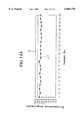
- FIG. 9shows graphs indicating a simulation test result for evaluating the thermal dissipation characteristics of packages according to the first to fourth embodiments of the present invention.
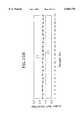
- FIG. 10shows graphs indicating the thermal resistance values shown in FIG. 9 in terms of the power dissipation values.
- FIGS. 11A to 11Care graphs showing the properties of bonding wires in the package according to the first embodiment of the present invention.
- FIGS. 12A to 12Care graphs showing the encapsulation property of the package according to the first embodiment of the present invention.
- FIGS. 13A to 13Care graphs showing the properties of bonding wires in the package according to the second embodiment of the present invention.
- FIGS. 14A to 14Care graphs showing the encapsulation property of the package according to the second embodiment of the present invention.
- FIGS. 15A to 15Care graphs showing the ball mount property of the package according to the second embodiment of the present invention.
- FIG. 3is a cross-sectional view showing a ball grid array package according to a first embodiment of this invention.
- the ball grid array package 100includes an interconnection substrate 50 comprising a first conductive trace layer 31a, a second conductive trace layer 31b, and an insulating layer 32 disposed between those layers 31a and 31b.
- Each of the first and second conductive trace layers 31a and 31bis comprised of many elements disposed in parallel to each other with a selected distance. The respective spaces between two of the many elements are filled with the insulating layer 32.
- the first and second conductive trace layersare preferably formed of copper.
- the interconnection substrate 50includes a first surface 50a exposed to the exterior of the package 100 and including one surface of the first conductive trace layer 31a and a second surface 50b opposed to the first surface 50a, including one surface of the second conductive trace layer 31b.
- the first surface 50a of the interconnection substrate 50includes one surface of the first conductive trace layer 31a and one surface of an insulating solder mask layer 33 formed such that the one surface of the first conductive trace layer 31a is exposed.
- On the first surface 50a of the interconnection substrate 50are attached a plurality of solder balls 34 serving as electrical contacts for making electrical connection of the interconnection substrate 50 with the exterior terminal (not shown) of the package 100.
- a metal thermal conductive layer 35serving as the heat sink through the adhesive preform 38. It is preferable to use as the adhesive preform 38 an adhesive tape having adhesive material at both surfaces although the liquid phase adhesive can be applied.
- the metal thermal conductive layer 35has a first surface 35a attached to the second surface 50b of the interconnection substrate 50, and a second surface 35b opposite the first surface 35a and exposed to the exterior of the package 100.
- the metal thermal conductive layer 35may, preferably, be made of copper, aluminum or silver.
- a hole region 36extending through them in a vertical direction.
- the hole region 36preferably, has a squared cross sectional shape along with circular shapes 37 at four corners thereof shown in FIG. 4 which is a plane view of the package 100.
- the hole region 36may have a rectangular, a circular, a diamond-like or a star-like shape in a cross sectional view and one of these shapes may have at edges thereof tetragonal shapes such as rectangular and diamond-like shapes, or at edges thereof triangular shapes.
- an integrated circuit chip 40having a first surface 40a exposed to the exterior of the package 100 and a second surface 40b opposite thereto.
- On the second surface 40b of the integrated circuit chip 40are formed a plurality of bond pads 41 and the bond pads 41 are electrically connected to the conductive trace layers 31a and 31b via bond wires 39.
- the heater block 61 shown in FIG.5is loaded on an assembly which comprises the interconnection substrate 50 and the metal thermal conductive layer 35 attached to the second surface 50b of the substrate 50 and in which the through hole region is formed at a central portion.
- the assemblyis formed as an unit.
- the second surface 35b of the metal thermal conductive layer 35faces the surface of the heater block 61.
- the process performed in such unitmay omit a siglulation step in the further process.
- the heater block 61has an evacuating hole 62 within the heater block 61.
- the evacuating hole 62serves as a vacuum chamber which is evacuated by a vacuum generating means (not shown).
- a person having an ordinary skill in the artcan easily think out various methods for forming a vacuum utilizing the evacuating hole in the heater block 61.
- a method of connecting the evacuating hole 62 via a hose to a vacuum generating means (not shown) which is disposed at an exterior of the heater block 61may be used.
- the evacuating hole 36is disposed within the hole region 36 with the second surface 35b of the metal thermal conductive layer 35 facing the surface of the heater block 61.
- an integrated circuit chip 40 sawed in an unitis disposed within the hole region 36 of the interconnection substrate 50, with the first surface 40a thereof covering the evacuating hole 62.
- the integrated circuit chip 40is aligned on the surface of the heater block 61, and thus is held on the surface thereof by a sucking force of vacuum acting on the first surface 40a via the evacuating hole from the vacuum generating means. Since the integrated circuit chip is held by such sucking force of vacuum, any die attachment process in the prior art is not required. Therefore, the package 100 according to this invention has thinner thickness and lower weight since die pads for the die attachment process are obviated from the package structure. Further, the method of manufacturing the package 100 has a benefit of reduced manufacturing cost since the die attachment process is obviated.
- a wire bonding step for making electrical connection of a plurality of bond pads 41 of the integrated circuit chip 40 with the interconnection substrate 50 via bond wires 39is carried out.
- the integrated circuit chip 40 and the bond wiresare then encapsulated by an epoxy-based encapsulant material 42 with filling the hole region 36, in a state in which the integrated circuit chip 40 is held on the surface of the heater block 61 by a sucking force of vacuum.
- the step of curing the encapsulant material 42is performed.
- solder balls 34are attached on the first surface 50a of the interconnection substrate 50 and a reflow process is then carried out.
- the second surface 40a of the integrated circuit chip 40is exposed to the exterior of the package 100, the heat created from the integrated circuit chip 40 can be easily dissipated into the exterior of the package 100.
- the package shown in FIG. 3shows a thermal resistance of 15.8° C./W in an air flow of 2 m/sec as the result of a simulation test for evaluating the heat dissipation characteristics of the package.
- the package according to this inventionhas a lower weight and a thinner thickness than in the prior art.
- the package shown in FIG. 3has a thickness of 1.0 mm and also has about 55% of the weight of the package shown in FIG. 2.
- the method according to the inventionhas various benefits such as reduced manufacturing time, reduced investment cost and reduced manufacturing cost.
- FIG. 6is a cross sectional view showing a ball grid array package 200 according to a second embodiment of this invention. Refer to an explanation of the components in FIG. 3 regarding the components not explained in FIG. 6.
- a ball grid array package 200includes a first metal thermal conductive layer 70 having a first surface 70a attached to the second surface 50b of the interconnection substrate 50 via an adhesive material 38 and a second surface 70b opposite to the first surface 70a, serving as a heat sink; and a second metal thermal conductive layer 73 attached to the first metal thermal conductive layer 70 via an adhesive material 72.
- the adhesive materials 38 and 72is a tape with adhesives at the both surface thereof.
- the second metal thermal conductive layer 73has a first surface 73a attached to the second surface 70b of the first metal thermal conductive layer 70 and a second surface 73b opposite to the first surface 73a, exposed to the exterior of the package 200.
- the second thermal conductive layer 73is shown in the foil shape in the drawings, the second thermal conductive layer may also be formed of a plurality of pins attached to the first metal thermal conductive layer 70 via the adhesive material 72. Further, at the central portion of the interconnection substrate 50 and the first metal thermal conductive layer 70 is formed a hole region 36 exposing the first surface 73a of the second metal thermal conductive layer 73.
- the integrated circuit chip 40having a first surface 40a attached to the first surface 73a of the second metal thermal conductive layer 73 via an adhesive 72 and a second surface opposite to the first surface 40a of the integrated circuit chip 40.
- the package 200 shown in FIG. 6may be manufactured by the same method as that of manufacturing the package 100 shown in FIG. 3, as described above. However, so as to manufacture the package 200, the method of manufacturing the package 200 further comprises the step of attaching the second metal thermal conductive layer 73 on the second surface 70b of the first metal thermal conductive layer 70 and the first surface 40a of the integrated circuit chip 40 by the adhesive 72 after the formation of the encapsulant material 42.
- the package 200 shown in FIG. 6has almost the same effect as the package 100 shown in FIG. 2.
- the package 200since the package 200 has the adhesive 72 formed all over the first surface of the second metal thermal conductive layer 73, the package 200 can more easily dissipate the heat created from the integrated circuit chip than the package shown in FIG. 2.
- the package 200 shown in FIG. 6has a thermal resistance of 6.3° C./W in an air flow of 2 m/sec, as the result of the simulation test for evaluating the heat dissipation characteristics of the package shown in FIG. 6.
- the second metal thermal conductive layer 73 in the package 200 shown in FIG. 6 as a heat sinkhas a thinner thickness since it is attached after forming the encapsulation 42.
- Such thin thickness of the second metal thermal conductive layeris highly contributed to the reduction of the total thickness and weight of the package 200.
- the package 200has a thickness of about 1.1 mm and has about 65% of the weight of the package shown in FIG. 2.
- FIG. 7is a cross sectional view showing a ball grid array package according to a third embodiment of this invention. Refer to the description of the package shown in FIG. 3 regarding the numerals not described in FIG. 7.
- a ball grid array package 300includes a second metal thermal conductive layer 83 attached to the second surface 70b of the first metal thermal conductive layer 70 by an adhesive 82.
- the adhesive 82is a tape with adhesives at both surfaces thereof.
- the second metal thermal conductive layer 83has a first surface 83a attached to the second surface 70b of the first metal thermal conductive layer 70 and a second 83b exposed to the exterior of the package 300 and also has a opening 84 at a central portion thereof.
- the second metal thermal conductive layer 83is shown in a shape of a foil, the second metal thermal conductive layer 83 may be made of a plurality of pins attached to the first metal thermal conductive layer 70 by the adhesive 82. At a central portion of the hole region 36 is disposed the integrated circuit chip 40 and the first surface 40a of the integrated circuit chip 40 is also in direct contact with the first surface 83a of the second metal thermal conductive layer 83.
- the package 300 shown in FIG. 7may be manufactured by almost the same method as that of manufacturing the package 100 shown in FIG. 3, as described above.
- the assembly in which the first and second metal conductive layers 70 and 83 are attached onto the interconnection substrate 50is loaded on the heater block 61, such that the second surface 83b of the second metal conductive layer 83 faces the surface of the heater block 61.
- the interconnection substrate 50 and the first metal conductive layer 70have the respective hole region 36 connected to each other.
- the integrated circuit chip 40is aligned and held on the hole region 36.
- the first surface 40a of the integrated circuit chip 40is in direct contact with the first surface 83a of the second metal conductive layer 83 by a sucking force of vacuum via the evacuating hole 62 and the opening 84 from the vacuum generating means.
- wire bonding, encapsulation and solder ball attachment processesare performed as described above regarding the manufacture of the package 100 shown in FIG. 3.
- the package 300 shown in FIG. 7has almost the same effects as the package 100 shown in FIG. 3. However, since the package 300 has a heat sink 83 of a shape such as a foil or a pin, the package 300 can more easily dissipate the heat created from the integrated circuit chip than the package 100.
- the package 300shows a thermal resistance of 7.8° C./W under an air flow of 2 m/sec as the result of simulation test for evaluating heat dissipation characteristics of the package.
- the package shown in FIG. 7has a thickness of 1.2 mm and has about 80% of the weight which the package shown in FIG. 2 has.
- FIG. 8is a cross-sectional view showing a ball grid array package 400 according to a fourth embodiment of this invention.
- the ball grid array package 400includes a metal thermal conductive metal layer 93 attached to an internal portion of the second surface 50b of the interconnection substrate 50 of the ball grid array package 400 by adhesive 92.
- the metal thermal conductive metal layer 93has a first surface 93a attached to the second surface of the interconnection substrate 50, and a second surface 93b which is exposed to an exterior and is opposite to the first surface 93a.
- the metal thermal conductive metal layer 93is preferable to be made of copper, silver or aluminum.
- the metal thermal conductive metal layer 93is copper, so as to prevent the corrosion the second surface 93b is plated with the material such as nickel. In the case that the metal thermal conductive layer 93 is aluminum, the second surface 93b is black-anodized.
- a hole region 36exposing the first surface 93a of the metal thermal conductive layer 93.
- an integrated circuit chip 40On a central portion of the hole region 36 is disposed an integrated circuit chip 40.
- the first surface 40a of the integrated circuit chip 40is attached to a first surface 93a of the metal thermal conductive layer 93 by an adhesive 95.
- the adhesive 95is preferable to contain silver so as to enhance the heat dissipation from the integrated circuit chip 40.
- a dielectric layer 96so as to prevent cracking and delamination of the package from moisture ingress through the metal thermal conductive layer 93 and the adhesive 92.
- An internal end portion of the dielectric layer 96is in contact with an end portion of the metal thermal conductive layer 93.
- the dielectric layer 96is preferable to be made of solder resist, polyimide or epoxy.
- the heater block 61 shown in FIG. 5is also used. Referring to FIG. 8 along with FIG. 5, the assembly in which the metal thermal conductive layer 93 and the dielectric layer 96 are attached onto the second surface 50b of the integrated circuit chip 50 is loaded on the heater block 61 such that the metal thermal conductive layer 93 and the dielectric layer 96 faces the surface of the heater block 61 equipped with the evacuating hole 62.
- the interconnection substrate 50 at its central portionhas a hole region 36.
- the second surface 93b of the metal thermal conductive layer 93is disposed on the heater block 61 with the perfect airtightness of the evacuating hole 62.
- a vacuum suctioning force generated by an operation of the vacuum apparatus connected to a heater block 61is applied to the second surface 93a of the metal thermal conductive layer 93 through the evacuating hole 62, so that the interconnection substrate 50 is held on the surface of the heater block 61.
- the bonding, encapsulation and solder ball attach processesare performed.
- the package 400 shown in FIG. 8has still thinner thickness and lower weight since the package 400 does not have a thermal conductive metal layer at a side portion of the integrated circuit chip 40. Also, since the thin thermal conductive layer 93 is attached as a heat sink to the first surface 40a of the integrated circuit chip 40, the package 400 is estimated to be as good as the packages shown in FIGS. 3, 6 and 7 in terms of heat dissipation performance. Unlike the packages 100, 200 and 300 shown in FIGS. 3, 6 and 7, in fabricating the package 400 after the attachment of the integrated circuit chip 40 to the metal thermal conductive layer 93 by the adhesives 95, a wire bonding process and an encapsulation process are performed on the heater block 61.
- the ball grid array package 400has benefits such as a reduced fabricating time, a reduced investment cost and a manufacturing cost since there is no need to carry out a molding process and a singulation process in fabricating the ball grid array package 400.
- the package shown in FIG. 7has a thickness of about 1.2 mm and has about 90% of the weight which the package shown in FIG. 2 has.
- FIG. 9is a graph showing the result of simulation test for evaluating heat dissipation characteristics of the packages according to the first to third embodiments of this invention.
- graph Ais a test result of the package according to the first embodiment of this invention
- graph Bis a test result of the package according to the second embodiment thereof
- graph Cis a test result of the package according to the third embodiment thereof
- the graph Dis a test result of the package according to the fourth embodiment thereof.
- the package according to the first embodimentshow excellent thermal resistances of 15.8° C./W at an air flow of 2 m/sec. , although it does not have the heat sink which is attached to the backside of the integrated circuit chip.
- Such the thermal resistance of the package according to the first embodimentis sufficient to dissipate the heat generated from the integrated chip.
- the package according to the second embodimentshows the most excellent thermal resistance of about 6.3° C./W at the air flow of 2 m/sec.
- the package according to the third embodimentshows the thermal resistance of about 7.8° C./W at the air flow of 2 m/sec.
- the package according to the fourth embodiment of this inventionshows the thermal resistance of about 6.5° C./W at the air flow of 2 m/sec.
- FIG. 10is a graph showing a conversion value of the thermal resistance values of FIG. 9 to power dissipation values.
- the axis of ordinatesshows power dispersion values in Watts
- the axis of abscissashows air flows in m/sec.
- graph Eshows power dissipation characteristic of the package according to the first embodiment of this invention
- graph Fshows that of the package according to the second embodiment thereof
- graph Gshows that of the package according to the third embodiment thereof
- graph Hshows that of the package according to the fourth embodiment of this invention.
- the packages according to this inventionshow excellent power dispersion characteristics of 3.2 Watts or more under an air flow of 2 m/sec.
- FIGS. 11(A) to (C)are graphs showing characteristics of the bond wire in the package according to the first embodiment of this invention.
- FIG. 11(A)shows the result of the bond pull test.
- FIG. 11(B)shows the result of ball shear test.
- FIG. 11(C)shows the result of measuring a loop height.
- K & S 1488 Turbo wire bonder manufactured by K & S company, Koreagold wire of 1.3 mils thickness manufactured by Mikyeong Sa, Korea and a capillary sold in the trademark of Micro Swiss 6 mil Tip were used.
- a wire bonding temperatureis 180° C.
- the timeis 25 msec for the first wire and the second wire, respectively
- the poweris 60 mW for the first wire and 120 mw for the second wire
- the forceis 45 g for the first wire and 110 g for the second wire.
- FIG. 11Ashows that as indicated in a graph I, 21 samples all have higher values than a reference value of more than 5 g (indicated in a graph J) in a bond pull test. Therefore, it is noted that strong wire-bonding is made.
- FIG. 11Bshows that as indicated in a graph K, 21 samples all have higher values than a reference value of more than 30 g in a ball shear test.
- 22 wire samplesall passed a reference value of less than 10 mils.
- FIGS. 12A to 12Care graphs showing the encapsulant characteristics of the package according to the first embodiment of this invention.
- FIG. 12Ashows the measurement result of the encapsulation height.
- FIG. 12Bshows the measurement result of a wire sweeping.
- FIG. 12Cis a measurement result of the void.
- a dispense systemsold in the trademark of CAMALO5000 and dam/fill material sold in the trademark of Hysol 4451/4450 were used.
- the encapsulation temperatureis 80° C. and the encapsulation pressure is 1.4 bar. As known from FIG.
- 22 samplespassed an encapsulation height reference value of less than 16 mils(indicated in a graph P).
- 22 samplespassed a reference value of less than 5.0% (indicated in a graph R) in a wire sweeping test.
- 22 samplespassed an encapsulation void ratio reference value of less than 5.0% (indicated in a graph T) in an encapsulation void ratio test.
- FIGS. 13A to 13Care graphs showing a bonding wire characteristic of the package according to the second embodiment of this invention.
- FIG. 13Ashows the result of a bond pull test.
- FIG. 13Bshows a result of a ball shear test.
- FIG. 13Cshows the result of a loop height test.
- K & S 1488 Turbo wire bondermanufactured by K & S company, Korea, gold wire of 1.3 mils diameter manufactured by Mikyeong Sa, Korea and a capillary sold in the trademark of STP were used.
- a wire bonding temperatureis 220° C.
- the timeis 25 msec for the first wire and is 30 msec for the second wire
- the poweris 60 mW for the first wire and for the second wire
- the forceis 45 g for the first wire and 55 g for the second wire.
- FIG. 13Ashows that as indicated in a graph U, 21 samples have a higher value than a reference value of more than 5 g(indicated in a graph V) in the bond pull test. Therefore, it is confirmed that a strong wire bonding is obtained.
- FIG. 13Bshows that as indicated in a graph W, all 21 samples pass over a reference value of more than 30 g (indicated in a graph X) in a ball shear test.
- FIG. 13Cshows that, as indicated in a graph Y, 22 wire samples all pass a reference value of 10 mils(indicated in a graph Z). From the above results, it is confirmed that a wire bonding work in a state in which the integrated circuit chip is attached on the heater block of FIG. 5 by a vacuum pressure can guarantee a successful wire bonding result.
- FIGS. 14A to 14Care graphs showing the encapsulation characteristic of the package according to a second embodiment of this invention wherein FIG. 14A shows the measured result of the encapsulation height, FIG. 4B shows the measured result of the wire sweeping and FIG. 4C shows the measured result of the encapsulation void.
- a dispense system sold in the trademark of CAMALO5000 and dam/fill material sold in the trademark of Hysol 4451/4450were used.
- the encapsulation temperatureis 80° C. and the encapsulation pressure is 1.5 bar.
- 22 samplespassed an encapsulation height reference value of 16 mils (indicated in a graph B1).
- 22 samplespassed a reference value of 5.0% (indicated in a graph D1) in a wire sweeping test.
- FIGS. 15A to 15Care graphs showing a ball mount characteristic of the package according to the second embodiment of this invention wherein FIG. 15A shows the measured result of a package warpage, FIG. 15B shows the measured result of a solder ball shear test and FIG. 15C shows the measured result of coplanarity.
- a ball mountersold in the trademark of SHIBUYA SBM-230, a furnace sold in the trademark of VITRONICS SMD-522N, a flux cleaner sold in the trademark of ACCEL MICROCEL 2 and a solder ball sold in the trademark of SENJU 63Sn/37Pb were used.
- FIG. 15Ashows that, as indicated in a graph G1, 12 samples all passed over a package warpage reference value of 5.0 mils(indicated in a graph H1). Furthermore, FIG. 15B shows that as indicated in a graph J1, 22 solder ball samples pass under a shear force reference value of less than 1 Kg(indicated in a graph K1). FIG. 15C shows that as indicated in graphs L1 and L2, 48 samples for 2 coplanarity tests where 24 samples are used for 1 coplanarity test pass under a coplanarity reference value of less than 6 mils(indicated in a graph M1). As known from the results of FIGS. 14A to 14C, it is confirmed that solder balls are mounted successfully in the package according to a second embodiment of this invention.
- the packages according to a third embodiment and a fourth embodiment of this inventiontests about a wire bonding characteristic, an encapsulant characteristic and a solder ball mount characteristic was not performed. However, though such tests are not carried out in this invention these inventors can anticipate that the packages according to the third embodiment and the fourth embodiment will have similar wire bonding characteristic, encapsulant characteristic, and solder ball mount characteristic as those according to the second embodiment of this invention since the packages according to the third embodiment and the fourth embodiment has a structural similarity to the package according to the second embodiment of this invention in that they each has a heat sink attached to the second surface of the integrated circuit chip.
- the ball grid array package according to this inventionhas the integrated circuit chip exposed to the exterior of the package or has a shallow pin or foil attached on the surface of the exposed integrated circuit chip. Therefore, the package according to this invention has benefits of excellent heat dissipation characteristic, low weight, a thin thickness and low manufacturing cost.
Landscapes
- Engineering & Computer Science (AREA)
- Microelectronics & Electronic Packaging (AREA)
- Physics & Mathematics (AREA)
- Condensed Matter Physics & Semiconductors (AREA)
- General Physics & Mathematics (AREA)
- Computer Hardware Design (AREA)
- Power Engineering (AREA)
- Chemical & Material Sciences (AREA)
- Materials Engineering (AREA)
- Cooling Or The Like Of Semiconductors Or Solid State Devices (AREA)
- Structures Or Materials For Encapsulating Or Coating Semiconductor Devices Or Solid State Devices (AREA)
Abstract
Description
Claims (8)
Applications Claiming Priority (4)
| Application Number | Priority Date | Filing Date | Title |
|---|---|---|---|
| KR97-19144 | 1997-05-17 | ||
| KR1019970019144AKR100220249B1 (en) | 1997-05-17 | 1997-05-17 | Thermally enhanced thin ball grid array package |
| KR1019970019145AKR19980083734A (en) | 1997-05-17 | 1997-05-17 | Thin Film Ball Grid Array Package with Improved Thermal Dissipation |
| KR97-19145 | 1997-07-21 |
Publications (1)
| Publication Number | Publication Date |
|---|---|
| US6060778Atrue US6060778A (en) | 2000-05-09 |
Family
ID=26632739
Family Applications (1)
| Application Number | Title | Priority Date | Filing Date |
|---|---|---|---|
| US09/060,981Expired - LifetimeUS6060778A (en) | 1997-05-17 | 1998-04-15 | Ball grid array package |
Country Status (6)
| Country | Link |
|---|---|
| US (1) | US6060778A (en) |
| JP (1) | JP3407184B2 (en) |
| CN (1) | CN100365804C (en) |
| DE (1) | DE19821715B4 (en) |
| GB (2) | GB2325340B (en) |
| TW (1) | TW449844B (en) |
Cited By (126)
| Publication number | Priority date | Publication date | Assignee | Title |
|---|---|---|---|---|
| US6196002B1 (en)* | 1999-06-24 | 2001-03-06 | Advanced Micro Devices, Inc. | Ball grid array package having thermoelectric cooler |
| WO2001037337A1 (en)* | 1999-11-15 | 2001-05-25 | Substrate Technologies, Inc. | Ball grid substrate for lead-on-chip semiconductor package |
| US6365967B1 (en)* | 1999-05-25 | 2002-04-02 | Micron Technology, Inc. | Interconnect structure |
| US6372539B1 (en) | 2000-03-20 | 2002-04-16 | National Semiconductor Corporation | Leadless packaging process using a conductive substrate |
| US6384471B1 (en)* | 1999-05-10 | 2002-05-07 | Bull S.A. | Pbga package with integrated ball grid |
| US6399415B1 (en) | 2000-03-20 | 2002-06-04 | National Semiconductor Corporation | Electrical isolation in panels of leadless IC packages |
| US6433360B1 (en)* | 1999-01-15 | 2002-08-13 | Xilinx, Inc. | Structure and method of testing failed or returned die to determine failure location and type |
| US20020127769A1 (en)* | 2000-10-18 | 2002-09-12 | Qing Ma | Method to protect an encapsulated die package during back grinding with a solder metallization layer and devices formed thereby |
| US6452278B1 (en) | 2000-06-30 | 2002-09-17 | Amkor Technology, Inc. | Low profile package for plural semiconductor dies |
| US6452255B1 (en)* | 2000-03-20 | 2002-09-17 | National Semiconductor, Corp. | Low inductance leadless package |
| US6459163B1 (en)* | 2001-03-21 | 2002-10-01 | United Test Center, Inc. | Semiconductor device and method for fabricating the same |
| US20020140085A1 (en)* | 2001-04-02 | 2002-10-03 | Lee Sang Ho | Semiconductor package including passive elements and method of manufacture |
| US6469258B1 (en) | 1999-08-24 | 2002-10-22 | Amkor Technology, Inc. | Circuit board for semiconductor package |
| US6475327B2 (en)* | 2001-04-05 | 2002-11-05 | Phoenix Precision Technology Corporation | Attachment of a stiff heat spreader for fabricating a cavity down plastic chip carrier |
| US6486537B1 (en)* | 2001-03-19 | 2002-11-26 | Amkor Technology, Inc. | Semiconductor package with warpage resistant substrate |
| US6501184B1 (en)* | 1999-05-20 | 2002-12-31 | Amkor Technology, Inc. | Semiconductor package and method for manufacturing the same |
| US6515356B1 (en) | 1999-05-07 | 2003-02-04 | Amkor Technology, Inc. | Semiconductor package and method for fabricating the same |
| US20030042581A1 (en)* | 2001-08-29 | 2003-03-06 | Fee Setho Sing | Packaged microelectronic devices and methods of forming same |
| US6541854B2 (en)* | 2000-12-01 | 2003-04-01 | Siliconware Precision Industries Co., Ltd. | Super low profile package with high efficiency of heat dissipation |
| US6555917B1 (en) | 2001-10-09 | 2003-04-29 | Amkor Technology, Inc. | Semiconductor package having stacked semiconductor chips and method of making the same |
| US6564454B1 (en) | 2000-12-28 | 2003-05-20 | Amkor Technology, Inc. | Method of making and stacking a semiconductor package |
| US20030104654A1 (en)* | 2000-06-28 | 2003-06-05 | Farnworth Warren M. | Recessed encapsulated microelectronic devices and methods for formation |
| US6576998B1 (en) | 2002-02-28 | 2003-06-10 | Amkor Technology, Inc. | Thin semiconductor package with semiconductor chip and electronic discrete device |
| US6624005B1 (en) | 2000-09-06 | 2003-09-23 | Amkor Technology, Inc. | Semiconductor memory cards and method of making same |
| US6651869B2 (en)* | 2001-09-21 | 2003-11-25 | Intel Corporation | Methods and electronic board products utilizing endothermic material for filling vias to absorb heat during wave soldering |
| US20040007771A1 (en)* | 1999-08-24 | 2004-01-15 | Amkor Technology, Inc. | Semiconductor package and method for fabricating the smae |
| US20040014258A1 (en)* | 1999-03-26 | 2004-01-22 | Akio Nakamura | Semiconductor device and method of fabricating the same |
| US6683795B1 (en) | 2002-04-10 | 2004-01-27 | Amkor Technology, Inc. | Shield cap and semiconductor package including shield cap |
| US6686652B1 (en) | 2000-03-20 | 2004-02-03 | National Semiconductor | Locking lead tips and die attach pad for a leadless package apparatus and method |
| US20040041166A1 (en)* | 2002-08-28 | 2004-03-04 | Morrison Michael W. | Ball grid array structures and tape-based method of manufacturing same |
| SG102640A1 (en)* | 2001-10-11 | 2004-03-26 | Ultratera Corp | Semiconductor device and method for fabricating the same |
| US20040100772A1 (en)* | 2002-11-22 | 2004-05-27 | Chye Lim Thiam | Packaged microelectronic component assemblies |
| US6747352B1 (en) | 2002-08-19 | 2004-06-08 | Amkor Technology, Inc. | Integrated circuit having multiple power/ground connections to a single external terminal |
| US6762489B2 (en) | 2001-11-20 | 2004-07-13 | International Business Machines Corporation | Jogging structure for wiring translation between grids with non-integral pitch ratios in chip carrier modules |
| US6784534B1 (en) | 2002-02-06 | 2004-08-31 | Amkor Technology, Inc. | Thin integrated circuit package having an optically transparent window |
| US20040173903A1 (en)* | 2003-03-06 | 2004-09-09 | Advanced Semiconductor Engineering Inc. | Thin type ball grid array package |
| US20040175916A1 (en)* | 1999-05-20 | 2004-09-09 | Amkor Technology, Inc. | Stackable semiconductor package having semiconductor chip within central through hole of substrate |
| US6833619B1 (en)* | 2003-04-28 | 2004-12-21 | Amkor Technology, Inc. | Thin profile semiconductor package which reduces warpage and damage during laser markings |
| US20050026325A1 (en)* | 2002-08-08 | 2005-02-03 | Koon Eng Meow | Packaged microelectronic components |
| US20050041398A1 (en)* | 2002-05-01 | 2005-02-24 | Huemoeller Ronald Patrick | Integrated circuit substrate having embedded back-side access conductors and vias |
| US20050051893A1 (en)* | 2003-09-05 | 2005-03-10 | Taiwan Semiconductor Manufacturing Co. | SBGA design for low-k integrated circuits (IC) |
| US20050082686A1 (en)* | 2003-10-17 | 2005-04-21 | Advanced Semiconductor Engineering, Inc. | Circuitized substrate for fixing solder beads on pads |
| US20050087864A1 (en)* | 2003-09-12 | 2005-04-28 | Advanced Semiconductor Engineering, Inc. | Cavity-down semiconductor package with heat spreader |
| US6936922B1 (en) | 2003-09-26 | 2005-08-30 | Amkor Technology, Inc. | Semiconductor package structure reducing warpage and manufacturing method thereof |
| US6967124B1 (en) | 2001-06-19 | 2005-11-22 | Amkor Technology, Inc. | Imprinted integrated circuit substrate and method for imprinting an integrated circuit substrate |
| US6982485B1 (en) | 2002-02-13 | 2006-01-03 | Amkor Technology, Inc. | Stacking structure for semiconductor chips and a semiconductor package using it |
| US20060035503A1 (en)* | 2003-08-29 | 2006-02-16 | Seng Eric T S | Invertible microfeature device packages and associated methods |
| US20060043600A1 (en)* | 2004-08-30 | 2006-03-02 | Masanori Onodera | Carrier structure for stacked-type semiconductor device, method of producing the same, and method of fabricating stacked-type semiconductor device |
| US7009296B1 (en) | 2004-01-15 | 2006-03-07 | Amkor Technology, Inc. | Semiconductor package with substrate coupled to a peripheral side surface of a semiconductor die |
| US7033664B2 (en) | 2002-10-22 | 2006-04-25 | Tessera Technologies Hungary Kft | Methods for producing packaged integrated circuit devices and packaged integrated circuit devices produced thereby |
| US7042072B1 (en) | 2002-08-02 | 2006-05-09 | Amkor Technology, Inc. | Semiconductor package and method of manufacturing the same which reduces warpage |
| US7145238B1 (en) | 2004-05-05 | 2006-12-05 | Amkor Technology, Inc. | Semiconductor package and substrate having multi-level vias |
| US7185426B1 (en) | 2002-05-01 | 2007-03-06 | Amkor Technology, Inc. | Method of manufacturing a semiconductor package |
| US20070145548A1 (en)* | 2003-12-22 | 2007-06-28 | Amkor Technology, Inc. | Stack-type semiconductor package and manufacturing method thereof |
| US20070158102A1 (en)* | 2006-01-12 | 2007-07-12 | Samsung Electronics Co., Ltd. | Method of attaching a high power surface mount transistor to a printed circuit board |
| US20070181989A1 (en)* | 2006-02-08 | 2007-08-09 | Micron Technology, Inc. | Microelectronic devices, stacked microelectronic devices, and methods for manufacturing such devices |
| US20070258215A1 (en)* | 2002-06-12 | 2007-11-08 | Samsung Electronics Co., Ltd. | High-power ball grid array package, heat spreader used in the bga package and method for manufacturing the same |
| US20080006928A1 (en)* | 2002-05-30 | 2008-01-10 | Taiyo Yuden Co., Ltd. | Composite multi-layer substrate and module using the substrate |
| CN100369243C (en)* | 2003-08-22 | 2008-02-13 | 矽品精密工业股份有限公司 | Semiconductor package with heat dissipation structure |
| US20080043447A1 (en)* | 2002-05-01 | 2008-02-21 | Amkor Technology, Inc. | Semiconductor package having laser-embedded terminals |
| USRE40112E1 (en) | 1999-05-20 | 2008-02-26 | Amkor Technology, Inc. | Semiconductor package and method for fabricating the same |
| US7334326B1 (en) | 2001-06-19 | 2008-02-26 | Amkor Technology, Inc. | Method for making an integrated circuit substrate having embedded passive components |
| US20080083981A1 (en)* | 2006-06-07 | 2008-04-10 | Romig Matthew D | Thermally Enhanced BGA Packages and Methods |
| US20080198552A1 (en)* | 2007-02-15 | 2008-08-21 | Samsung Electro-Mechanics Co., Ltd. | Package board and method for manufacturing thereof |
| US7429799B1 (en) | 2005-07-27 | 2008-09-30 | Amkor Technology, Inc. | Land patterns for a semiconductor stacking structure and method therefor |
| US20080237589A1 (en)* | 2007-03-29 | 2008-10-02 | Casio Computer Co. Ltd. | Semiconductor device comprising circuit substrate with inspection connection pads and manufacturing method thereof |
| US7501338B1 (en) | 2001-06-19 | 2009-03-10 | Amkor Technology, Inc. | Semiconductor package substrate fabrication method |
| US20090096076A1 (en)* | 2007-10-16 | 2009-04-16 | Jung Young Hy | Stacked semiconductor package without reduction in stata storage capacity and method for manufacturing the same |
| US7548430B1 (en) | 2002-05-01 | 2009-06-16 | Amkor Technology, Inc. | Buildup dielectric and metallization process and semiconductor package |
| US7550857B1 (en) | 2006-11-16 | 2009-06-23 | Amkor Technology, Inc. | Stacked redistribution layer (RDL) die assembly package |
| US7589398B1 (en) | 2006-10-04 | 2009-09-15 | Amkor Technology, Inc. | Embedded metal features structure |
| US20090269891A1 (en)* | 2006-01-30 | 2009-10-29 | Marvel World Trade Ltd. | Thermal enhanced package |
| US20090306811A1 (en)* | 2008-06-06 | 2009-12-10 | Raytheon Company | Ball grid array cleaning system |
| US7633765B1 (en) | 2004-03-23 | 2009-12-15 | Amkor Technology, Inc. | Semiconductor package including a top-surface metal layer for implementing circuit features |
| US20100006332A1 (en)* | 2007-02-09 | 2010-01-14 | Panasonic Corporation | Circuit board, laminating circuit board and electronic apparatus |
| US7670962B2 (en) | 2002-05-01 | 2010-03-02 | Amkor Technology, Inc. | Substrate having stiffener fabrication method |
| US20100120206A1 (en)* | 2006-12-12 | 2010-05-13 | Agere Systems, Inc. | Integrated circuit package and a method for dissipating heat in an integrated circuit package |
| AU2007203504B2 (en)* | 2001-03-21 | 2010-05-27 | United Test Center Inc | Semi Conductor Device and Method for Fabricating The Same |
| US7750250B1 (en) | 2006-12-22 | 2010-07-06 | Amkor Technology, Inc. | Blind via capture pad structure |
| US7752752B1 (en) | 2007-01-09 | 2010-07-13 | Amkor Technology, Inc. | Method of fabricating an embedded circuit pattern |
| US7960827B1 (en) | 2009-04-09 | 2011-06-14 | Amkor Technology, Inc. | Thermal via heat spreader package and method |
| US20110215444A1 (en)* | 2010-03-08 | 2011-09-08 | Samsung Electronics Co., Ltd | Package substrates, semiconductor packages having the same, and methods of fabricating the semiconductor packages |
| US8222538B1 (en) | 2009-06-12 | 2012-07-17 | Amkor Technology, Inc. | Stackable via package and method |
| US8294276B1 (en) | 2010-05-27 | 2012-10-23 | Amkor Technology, Inc. | Semiconductor device and fabricating method thereof |
| US8300423B1 (en) | 2010-05-25 | 2012-10-30 | Amkor Technology, Inc. | Stackable treated via package and method |
| US8323771B1 (en) | 2007-08-15 | 2012-12-04 | Amkor Technology, Inc. | Straight conductor blind via capture pad structure and fabrication method |
| US8338229B1 (en) | 2010-07-30 | 2012-12-25 | Amkor Technology, Inc. | Stackable plasma cleaned via package and method |
| US8337657B1 (en) | 2010-10-27 | 2012-12-25 | Amkor Technology, Inc. | Mechanical tape separation package and method |
| US8471154B1 (en) | 2009-08-06 | 2013-06-25 | Amkor Technology, Inc. | Stackable variable height via package and method |
| US8482134B1 (en) | 2010-11-01 | 2013-07-09 | Amkor Technology, Inc. | Stackable package and method |
| US8525318B1 (en) | 2010-11-10 | 2013-09-03 | Amkor Technology, Inc. | Semiconductor device and fabricating method thereof |
| US8535961B1 (en) | 2010-12-09 | 2013-09-17 | Amkor Technology, Inc. | Light emitting diode (LED) package and method |
| US8536462B1 (en) | 2010-01-22 | 2013-09-17 | Amkor Technology, Inc. | Flex circuit package and method |
| US8557629B1 (en) | 2010-12-03 | 2013-10-15 | Amkor Technology, Inc. | Semiconductor device having overlapped via apertures |
| US8623753B1 (en) | 2009-05-28 | 2014-01-07 | Amkor Technology, Inc. | Stackable protruding via package and method |
| US8633598B1 (en) | 2011-09-20 | 2014-01-21 | Amkor Technology, Inc. | Underfill contacting stacking balls package fabrication method and structure |
| US20140027051A1 (en)* | 2011-09-29 | 2014-01-30 | Viking Tech Corporation | Method of Fabricating a Light Emitting Diode Packaging Structure |
| US8653674B1 (en) | 2011-09-15 | 2014-02-18 | Amkor Technology, Inc. | Electronic component package fabrication method and structure |
| US8717775B1 (en) | 2010-08-02 | 2014-05-06 | Amkor Technology, Inc. | Fingerprint sensor package and method |
| US20140133119A1 (en)* | 2010-03-30 | 2014-05-15 | Ibiden Co., Ltd. | Wiring board and method for manufacturing the same |
| CN103887278A (en)* | 2012-12-19 | 2014-06-25 | 英特尔公司 | Encapsulation and Dielectric or Anisotropically Conductive (ACF) Construction Layers |
| US8796561B1 (en) | 2009-10-05 | 2014-08-05 | Amkor Technology, Inc. | Fan out build up substrate stackable package and method |
| US8826531B1 (en) | 2005-04-05 | 2014-09-09 | Amkor Technology, Inc. | Method for making an integrated circuit substrate having laminated laser-embedded circuit layers |
| US8872329B1 (en) | 2009-01-09 | 2014-10-28 | Amkor Technology, Inc. | Extended landing pad substrate package structure and method |
| US8890329B2 (en) | 2011-04-26 | 2014-11-18 | Amkor Technology, Inc. | Semiconductor device |
| US20150004748A1 (en)* | 2013-06-27 | 2015-01-01 | Stats Chippac, Ltd. | Methods of Forming Conductive Jumper Traces |
| US8937381B1 (en) | 2009-12-03 | 2015-01-20 | Amkor Technology, Inc. | Thin stackable package and method |
| US9013011B1 (en) | 2011-03-11 | 2015-04-21 | Amkor Technology, Inc. | Stacked and staggered die MEMS package and method |
| US9029962B1 (en) | 2011-10-12 | 2015-05-12 | Amkor Technology, Inc. | Molded cavity substrate MEMS package fabrication method and structure |
| US9391043B2 (en) | 2012-11-20 | 2016-07-12 | Amkor Technology, Inc. | Semiconductor device and manufacturing method thereof |
| US9466545B1 (en) | 2007-02-21 | 2016-10-11 | Amkor Technology, Inc. | Semiconductor package in package |
| US9543242B1 (en) | 2013-01-29 | 2017-01-10 | Amkor Technology, Inc. | Semiconductor package and fabricating method thereof |
| US9691635B1 (en) | 2002-05-01 | 2017-06-27 | Amkor Technology, Inc. | Buildup dielectric layer having metallization pattern semiconductor package fabrication method |
| US9691734B1 (en) | 2009-12-07 | 2017-06-27 | Amkor Technology, Inc. | Method of forming a plurality of electronic component packages |
| US9704747B2 (en) | 2013-03-29 | 2017-07-11 | Amkor Technology, Inc. | Semiconductor device and manufacturing method thereof |
| US9704842B2 (en) | 2013-11-04 | 2017-07-11 | Amkor Technology, Inc. | Interposer, manufacturing method thereof, semiconductor package using the same, and method for fabricating the semiconductor package |
| US20170207205A1 (en)* | 2016-01-14 | 2017-07-20 | Jichul Kim | Semiconductor packages |
| US9721872B1 (en) | 2011-02-18 | 2017-08-01 | Amkor Technology, Inc. | Methods and structures for increasing the allowable die size in TMV packages |
| US9748154B1 (en) | 2010-11-04 | 2017-08-29 | Amkor Technology, Inc. | Wafer level fan out semiconductor device and manufacturing method thereof |
| US9960328B2 (en) | 2016-09-06 | 2018-05-01 | Amkor Technology, Inc. | Semiconductor device and manufacturing method thereof |
| US10811277B2 (en) | 2004-03-23 | 2020-10-20 | Amkor Technology, Inc. | Encapsulated semiconductor package |
| US10832991B1 (en)* | 2019-05-07 | 2020-11-10 | Texas Instruments Incorporated | Leadless packaged device with metal die attach |
| CN112307710A (en)* | 2020-12-21 | 2021-02-02 | 北京智芯仿真科技有限公司 | Direct current voltage drop analysis method and system of system-level integrated circuit |
| US10937771B2 (en) | 2016-01-14 | 2021-03-02 | Samsung Electronics Co., Ltd. | Semiconductor packages |
| US11081370B2 (en) | 2004-03-23 | 2021-08-03 | Amkor Technology Singapore Holding Pte. Ltd. | Methods of manufacturing an encapsulated semiconductor device |
| US11545448B2 (en)* | 2019-07-11 | 2023-01-03 | Thales | Moisture-resistant electronic component and process for producing such a component |
Families Citing this family (18)
| Publication number | Priority date | Publication date | Assignee | Title |
|---|---|---|---|---|
| JP2000150730A (en)* | 1998-11-17 | 2000-05-30 | Fujitsu Ltd | Semiconductor device and manufacturing method thereof |
| DE10042839B4 (en)* | 2000-08-30 | 2009-01-29 | Infineon Technologies Ag | Electronic component with heat sink and method for its production |
| JP4085788B2 (en)* | 2002-08-30 | 2008-05-14 | 日本電気株式会社 | SEMICONDUCTOR DEVICE AND ITS MANUFACTURING METHOD, CIRCUIT BOARD, ELECTRONIC DEVICE |
| CN100364074C (en)* | 2003-04-29 | 2008-01-23 | 半导体元件工业有限责任公司 | Method of making a low profile highly-packaged semiconductor device |
| CN1327514C (en)* | 2003-10-01 | 2007-07-18 | 松下电器产业株式会社 | Wiring substrate and method of manufacturing the same |
| CN100433278C (en)* | 2004-10-29 | 2008-11-12 | 矽品精密工业股份有限公司 | Heat dissipation type packaging structure and manufacturing method thereof |
| CN1319139C (en)* | 2004-12-01 | 2007-05-30 | 中国电子科技集团公司第二十四研究所 | Production of local vacuum sealing protective structure of silicon based sensor flexible piece |
| CN100446200C (en)* | 2005-02-28 | 2008-12-24 | 矽品精密工业股份有限公司 | Heat dissipation type package structure and manufacturing method thereof |
| CN100481420C (en)* | 2005-09-08 | 2009-04-22 | 南茂科技股份有限公司 | Stacked chip packaging structure, chip packaging body and manufacturing method thereof |
| CN101494205B (en)* | 2008-01-23 | 2011-02-02 | 瑞鼎科技股份有限公司 | Integrated circuit package and manufacturing method thereof |
| KR101481405B1 (en)* | 2008-06-12 | 2015-01-22 | 삼성전자주식회사 | semiconductor apparatus and manufacturing method of the same |
| JPWO2010095367A1 (en)* | 2009-02-19 | 2012-08-23 | 日本電気株式会社 | Vacuum sealed package, printed circuit board having vacuum sealed package, electronic device, and manufacturing method of vacuum sealed package |
| US8097956B2 (en)* | 2009-03-12 | 2012-01-17 | Apple Inc. | Flexible packaging for chip-on-chip and package-on-package technologies |
| CN102867814A (en)* | 2011-07-06 | 2013-01-09 | 鸿富锦精密工业(深圳)有限公司 | Chip packaging body |
| EP2881986A3 (en)* | 2013-12-06 | 2015-08-12 | Ka Wa Cheung | System and method for manufacturing a cavity down fabricated carrier |
| SG10201400390YA (en)* | 2014-03-05 | 2015-10-29 | Delta Electronics Int L Singapore Pte Ltd | Package structure |
| CN105070694A (en)* | 2015-08-24 | 2015-11-18 | 中国科学院国家空间科学中心 | A packaging method for exposing chip substrate surface |
| CN106298696B (en)* | 2016-08-22 | 2018-10-09 | 陶乐敏 | A kind of integrated antenna package mechanism of suspension-type |
Citations (17)
| Publication number | Priority date | Publication date | Assignee | Title |
|---|---|---|---|---|
| GB2136205A (en)* | 1983-03-09 | 1984-09-12 | Printed Circuits Int | Semiconductor chip carrier and contact array package and method of construction |
| GB2189084A (en)* | 1986-04-10 | 1987-10-14 | Stc Plc | Integrated circuit packaging |
| US4835598A (en)* | 1985-06-13 | 1989-05-30 | Matsushita Electric Works, Ltd. | Wiring board |
| US4897508A (en)* | 1988-02-10 | 1990-01-30 | Olin Corporation | Metal electronic package |
| US5105259A (en)* | 1990-09-28 | 1992-04-14 | Motorola, Inc. | Thermally enhanced semiconductor device utilizing a vacuum to ultimately enhance thermal dissipation |
| JPH04119653A (en)* | 1990-09-11 | 1992-04-21 | Toppan Printing Co Ltd | Integrated circuit element |
| US5147821A (en)* | 1990-09-28 | 1992-09-15 | Motorola, Inc. | Method for making a thermally enhanced semiconductor device by holding a leadframe against a heatsink through vacuum suction in a molding operation |
| US5404273A (en)* | 1993-03-23 | 1995-04-04 | Shinko Electric Industries Co., Ltd. | Semiconductor-device package and semiconductor device |
| US5583378A (en)* | 1994-05-16 | 1996-12-10 | Amkor Electronics, Inc. | Ball grid array integrated circuit package with thermal conductor |
| KR970013234A (en)* | 1995-08-07 | 1997-03-29 | 원본미기재 | Packaged integrated circuit device and its manufacturing method |
| US5672909A (en)* | 1995-02-07 | 1997-09-30 | Amkor Electronics, Inc. | Interdigitated wirebond programmable fixed voltage planes |
| US5689091A (en)* | 1996-09-19 | 1997-11-18 | Vlsi Technology, Inc. | Multi-layer substrate structure |
| US5708567A (en)* | 1995-11-15 | 1998-01-13 | Anam Industrial Co., Ltd. | Ball grid array semiconductor package with ring-type heat sink |
| US5777387A (en)* | 1995-09-29 | 1998-07-07 | Nec Corporation | Semiconductor device constructed by mounting a semiconductor chip on a film carrier tape |
| US5796170A (en)* | 1996-02-15 | 1998-08-18 | Northern Telecom Limited | Ball grid array (BGA) integrated circuit packages |
| US5814883A (en)* | 1995-10-04 | 1998-09-29 | Mitsubishi Denki Kabushiki Kaisha | Packaged semiconductor chip |
| US5844168A (en)* | 1995-08-01 | 1998-12-01 | Minnesota Mining And Manufacturing Company | Multi-layer interconnect sutructure for ball grid arrays |
Family Cites Families (5)
| Publication number | Priority date | Publication date | Assignee | Title |
|---|---|---|---|---|
| JPH05102212A (en)* | 1991-10-04 | 1993-04-23 | Seiko Epson Corp | Wiring board |
| JPH05283553A (en)* | 1992-03-30 | 1993-10-29 | Nec Corp | Hybrid integrated circuit device |
| US5291062A (en)* | 1993-03-01 | 1994-03-01 | Motorola, Inc. | Area array semiconductor device having a lid with functional contacts |
| US5572405A (en)* | 1995-06-07 | 1996-11-05 | International Business Machines Corporation (Ibm) | Thermally enhanced ball grid array package |
| JPH09129784A (en)* | 1995-10-27 | 1997-05-16 | Fuji Xerox Co Ltd | Semiconductor device and manufacture thereof |
- 1998
- 1998-03-12TWTW087103626Apatent/TW449844B/ennot_activeIP Right Cessation
- 1998-03-20GBGB9806078Apatent/GB2325340B/ennot_activeExpired - Fee Related
- 1998-03-27JPJP10042898Apatent/JP3407184B2/ennot_activeExpired - Fee Related
- 1998-04-15USUS09/060,981patent/US6060778A/ennot_activeExpired - Lifetime
- 1998-05-06CNCNB981079326Apatent/CN100365804C/ennot_activeExpired - Fee Related
- 1998-05-14DEDE19821715Apatent/DE19821715B4/ennot_activeExpired - Fee Related
- 2002
- 2002-06-05GBGBGB0212903.9Apatent/GB0212903D0/ennot_activeCeased
Patent Citations (17)
| Publication number | Priority date | Publication date | Assignee | Title |
|---|---|---|---|---|
| GB2136205A (en)* | 1983-03-09 | 1984-09-12 | Printed Circuits Int | Semiconductor chip carrier and contact array package and method of construction |
| US4835598A (en)* | 1985-06-13 | 1989-05-30 | Matsushita Electric Works, Ltd. | Wiring board |
| GB2189084A (en)* | 1986-04-10 | 1987-10-14 | Stc Plc | Integrated circuit packaging |
| US4897508A (en)* | 1988-02-10 | 1990-01-30 | Olin Corporation | Metal electronic package |
| JPH04119653A (en)* | 1990-09-11 | 1992-04-21 | Toppan Printing Co Ltd | Integrated circuit element |
| US5105259A (en)* | 1990-09-28 | 1992-04-14 | Motorola, Inc. | Thermally enhanced semiconductor device utilizing a vacuum to ultimately enhance thermal dissipation |
| US5147821A (en)* | 1990-09-28 | 1992-09-15 | Motorola, Inc. | Method for making a thermally enhanced semiconductor device by holding a leadframe against a heatsink through vacuum suction in a molding operation |
| US5404273A (en)* | 1993-03-23 | 1995-04-04 | Shinko Electric Industries Co., Ltd. | Semiconductor-device package and semiconductor device |
| US5583378A (en)* | 1994-05-16 | 1996-12-10 | Amkor Electronics, Inc. | Ball grid array integrated circuit package with thermal conductor |
| US5672909A (en)* | 1995-02-07 | 1997-09-30 | Amkor Electronics, Inc. | Interdigitated wirebond programmable fixed voltage planes |
| US5844168A (en)* | 1995-08-01 | 1998-12-01 | Minnesota Mining And Manufacturing Company | Multi-layer interconnect sutructure for ball grid arrays |
| KR970013234A (en)* | 1995-08-07 | 1997-03-29 | 원본미기재 | Packaged integrated circuit device and its manufacturing method |
| US5777387A (en)* | 1995-09-29 | 1998-07-07 | Nec Corporation | Semiconductor device constructed by mounting a semiconductor chip on a film carrier tape |
| US5814883A (en)* | 1995-10-04 | 1998-09-29 | Mitsubishi Denki Kabushiki Kaisha | Packaged semiconductor chip |
| US5708567A (en)* | 1995-11-15 | 1998-01-13 | Anam Industrial Co., Ltd. | Ball grid array semiconductor package with ring-type heat sink |
| US5796170A (en)* | 1996-02-15 | 1998-08-18 | Northern Telecom Limited | Ball grid array (BGA) integrated circuit packages |
| US5689091A (en)* | 1996-09-19 | 1997-11-18 | Vlsi Technology, Inc. | Multi-layer substrate structure |
Non-Patent Citations (4)
| Title |
|---|
| English translation of Purpose and Constitution for JP 4119653 A (Apr. 21, 1992).* |
| English translation of Purpose and Constitution for JP4-119653 (Apr. 21, 1992). |
| English translation of Purpose and Constitution for KR 97013234 A (Mar. 29, 1997).* |
| English translation of Purpose and Constitution for KR97-13234 (Mar. 29, 1997). |
Cited By (252)
| Publication number | Priority date | Publication date | Assignee | Title |
|---|---|---|---|---|
| US6768329B1 (en) | 1999-01-15 | 2004-07-27 | Xilinx Inc. | Structure and method of testing failed or returned die to determine failure location and type |
| US6433360B1 (en)* | 1999-01-15 | 2002-08-13 | Xilinx, Inc. | Structure and method of testing failed or returned die to determine failure location and type |
| US20040014258A1 (en)* | 1999-03-26 | 2004-01-22 | Akio Nakamura | Semiconductor device and method of fabricating the same |
| US6982478B2 (en)* | 1999-03-26 | 2006-01-03 | Oki Electric Industry Co., Ltd. | Semiconductor device and method of fabricating the same |
| US6717248B2 (en) | 1999-05-07 | 2004-04-06 | Amkor Technology, Inc. | Semiconductor package and method for fabricating the same |
| US6515356B1 (en) | 1999-05-07 | 2003-02-04 | Amkor Technology, Inc. | Semiconductor package and method for fabricating the same |
| US7190071B2 (en) | 1999-05-07 | 2007-03-13 | Amkor Technology, Inc. | Semiconductor package and method for fabricating the same |
| US6384471B1 (en)* | 1999-05-10 | 2002-05-07 | Bull S.A. | Pbga package with integrated ball grid |
| US7061120B2 (en) | 1999-05-20 | 2006-06-13 | Amkor Technology, Inc. | Stackable semiconductor package having semiconductor chip within central through hole of substrate |
| US6830955B2 (en)* | 1999-05-20 | 2004-12-14 | Amkor Technology, Inc. | Semiconductor package and method for manufacturing the same |
| USRE40112E1 (en) | 1999-05-20 | 2008-02-26 | Amkor Technology, Inc. | Semiconductor package and method for fabricating the same |
| US20040175916A1 (en)* | 1999-05-20 | 2004-09-09 | Amkor Technology, Inc. | Stackable semiconductor package having semiconductor chip within central through hole of substrate |
| US20030001285A1 (en)* | 1999-05-20 | 2003-01-02 | Amkor Technology, Inc. | Semiconductor package and method for manufacturing the same |
| US6501184B1 (en)* | 1999-05-20 | 2002-12-31 | Amkor Technology, Inc. | Semiconductor package and method for manufacturing the same |
| US6365967B1 (en)* | 1999-05-25 | 2002-04-02 | Micron Technology, Inc. | Interconnect structure |
| US6196002B1 (en)* | 1999-06-24 | 2001-03-06 | Advanced Micro Devices, Inc. | Ball grid array package having thermoelectric cooler |
| US20050205979A1 (en)* | 1999-08-24 | 2005-09-22 | Shin Won S | Semiconductor package and method for fabricating the same |
| US6798049B1 (en) | 1999-08-24 | 2004-09-28 | Amkor Technology Inc. | Semiconductor package and method for fabricating the same |
| US6469258B1 (en) | 1999-08-24 | 2002-10-22 | Amkor Technology, Inc. | Circuit board for semiconductor package |
| US7211900B2 (en) | 1999-08-24 | 2007-05-01 | Amkor Technology, Inc. | Thin semiconductor package including stacked dies |
| US20040007771A1 (en)* | 1999-08-24 | 2004-01-15 | Amkor Technology, Inc. | Semiconductor package and method for fabricating the smae |
| US6982488B2 (en) | 1999-08-24 | 2006-01-03 | Amkor Technology, Inc. | Semiconductor package and method for fabricating the same |
| US6534861B1 (en)* | 1999-11-15 | 2003-03-18 | Substrate Technologies Incorporated | Ball grid substrate for lead-on-chip semiconductor package |
| US20030132518A1 (en)* | 1999-11-15 | 2003-07-17 | Castro Abram M. | Ball grid substrate for lead-on-chip semiconductor package |
| WO2001037337A1 (en)* | 1999-11-15 | 2001-05-25 | Substrate Technologies, Inc. | Ball grid substrate for lead-on-chip semiconductor package |
| US6372539B1 (en) | 2000-03-20 | 2002-04-16 | National Semiconductor Corporation | Leadless packaging process using a conductive substrate |
| US6399415B1 (en) | 2000-03-20 | 2002-06-04 | National Semiconductor Corporation | Electrical isolation in panels of leadless IC packages |
| US6686652B1 (en) | 2000-03-20 | 2004-02-03 | National Semiconductor | Locking lead tips and die attach pad for a leadless package apparatus and method |
| US6452255B1 (en)* | 2000-03-20 | 2002-09-17 | National Semiconductor, Corp. | Low inductance leadless package |
| US6841423B2 (en)* | 2000-06-28 | 2005-01-11 | Micron Technology, Inc. | Methods for formation of recessed encapsulated microelectronic devices |
| US20030104654A1 (en)* | 2000-06-28 | 2003-06-05 | Farnworth Warren M. | Recessed encapsulated microelectronic devices and methods for formation |
| US6819003B2 (en) | 2000-06-28 | 2004-11-16 | Micron Technology Inc. | Recessed encapsulated microelectronic devices and methods for formation |
| US6452278B1 (en) | 2000-06-30 | 2002-09-17 | Amkor Technology, Inc. | Low profile package for plural semiconductor dies |
| US8258613B1 (en) | 2000-09-06 | 2012-09-04 | Amkor Technology, Inc. | Semiconductor memory card |
| US6624005B1 (en) | 2000-09-06 | 2003-09-23 | Amkor Technology, Inc. | Semiconductor memory cards and method of making same |
| US6964889B2 (en) | 2000-10-18 | 2005-11-15 | Intel Corporation | Method to protect an encapsulated die package during back grinding with a solder metallization layer and devices formed thereby |
| US6902950B2 (en)* | 2000-10-18 | 2005-06-07 | Intel Corporation | Method to protect an encapsulated die package during back grinding with a solder metallization layer and devices formed thereby |
| US20020127780A1 (en)* | 2000-10-18 | 2002-09-12 | Qing Ma | Method to protect an encapsulated die package during back grinding with a solder metallization layer and devices formed thereby |
| US20020127769A1 (en)* | 2000-10-18 | 2002-09-12 | Qing Ma | Method to protect an encapsulated die package during back grinding with a solder metallization layer and devices formed thereby |
| US6713321B2 (en)* | 2000-12-01 | 2004-03-30 | Siliconware Precision Industries Co. Ltd. | Super low profile package with high efficiency of heat dissipation |
| US20030092221A1 (en)* | 2000-12-01 | 2003-05-15 | Chien-Ping Huang | Super low profile package with high efficiency of heat dissipation |
| US6541854B2 (en)* | 2000-12-01 | 2003-04-01 | Siliconware Precision Industries Co., Ltd. | Super low profile package with high efficiency of heat dissipation |
| US6564454B1 (en) | 2000-12-28 | 2003-05-20 | Amkor Technology, Inc. | Method of making and stacking a semiconductor package |
| US6486537B1 (en)* | 2001-03-19 | 2002-11-26 | Amkor Technology, Inc. | Semiconductor package with warpage resistant substrate |
| US6964888B2 (en)* | 2001-03-21 | 2005-11-15 | Ultratera Corporation | Semiconductor device and method for fabricating the same |
| US6790712B2 (en) | 2001-03-21 | 2004-09-14 | United Test Center, Inc. | Semiconductor device and method for fabricating the same |
| US6459163B1 (en)* | 2001-03-21 | 2002-10-01 | United Test Center, Inc. | Semiconductor device and method for fabricating the same |
| AU2007203504B2 (en)* | 2001-03-21 | 2010-05-27 | United Test Center Inc | Semi Conductor Device and Method for Fabricating The Same |
| US20020192860A1 (en)* | 2001-03-21 | 2002-12-19 | Jin-Chuan Bai | Semiconductor device and method for fabricating the same |
| US6995448B2 (en) | 2001-04-02 | 2006-02-07 | Amkor Technology, Inc. | Semiconductor package including passive elements and method of manufacture |
| US20020140085A1 (en)* | 2001-04-02 | 2002-10-03 | Lee Sang Ho | Semiconductor package including passive elements and method of manufacture |
| US6475327B2 (en)* | 2001-04-05 | 2002-11-05 | Phoenix Precision Technology Corporation | Attachment of a stiff heat spreader for fabricating a cavity down plastic chip carrier |
| US6967124B1 (en) | 2001-06-19 | 2005-11-22 | Amkor Technology, Inc. | Imprinted integrated circuit substrate and method for imprinting an integrated circuit substrate |
| US7334326B1 (en) | 2001-06-19 | 2008-02-26 | Amkor Technology, Inc. | Method for making an integrated circuit substrate having embedded passive components |
| US7501338B1 (en) | 2001-06-19 | 2009-03-10 | Amkor Technology, Inc. | Semiconductor package substrate fabrication method |
| US6943450B2 (en) | 2001-08-29 | 2005-09-13 | Micron Technology, Inc. | Packaged microelectronic devices and methods of forming same |
| US20050023655A1 (en)* | 2001-08-29 | 2005-02-03 | Fee Setho Sing | Packaged microelectronic devices and methods of forming same |
| US20030042581A1 (en)* | 2001-08-29 | 2003-03-06 | Fee Setho Sing | Packaged microelectronic devices and methods of forming same |
| US6876066B2 (en) | 2001-08-29 | 2005-04-05 | Micron Technology, Inc. | Packaged microelectronic devices and methods of forming same |
| US6651869B2 (en)* | 2001-09-21 | 2003-11-25 | Intel Corporation | Methods and electronic board products utilizing endothermic material for filling vias to absorb heat during wave soldering |
| US6555917B1 (en) | 2001-10-09 | 2003-04-29 | Amkor Technology, Inc. | Semiconductor package having stacked semiconductor chips and method of making the same |
| SG102640A1 (en)* | 2001-10-11 | 2004-03-26 | Ultratera Corp | Semiconductor device and method for fabricating the same |
| US6762489B2 (en) | 2001-11-20 | 2004-07-13 | International Business Machines Corporation | Jogging structure for wiring translation between grids with non-integral pitch ratios in chip carrier modules |
| US6784534B1 (en) | 2002-02-06 | 2004-08-31 | Amkor Technology, Inc. | Thin integrated circuit package having an optically transparent window |
| US6982485B1 (en) | 2002-02-13 | 2006-01-03 | Amkor Technology, Inc. | Stacking structure for semiconductor chips and a semiconductor package using it |
| US6576998B1 (en) | 2002-02-28 | 2003-06-10 | Amkor Technology, Inc. | Thin semiconductor package with semiconductor chip and electronic discrete device |
| US6683795B1 (en) | 2002-04-10 | 2004-01-27 | Amkor Technology, Inc. | Shield cap and semiconductor package including shield cap |
| US7185426B1 (en) | 2002-05-01 | 2007-03-06 | Amkor Technology, Inc. | Method of manufacturing a semiconductor package |
| US7670962B2 (en) | 2002-05-01 | 2010-03-02 | Amkor Technology, Inc. | Substrate having stiffener fabrication method |
| US10461006B1 (en) | 2002-05-01 | 2019-10-29 | Amkor Technology, Inc. | Encapsulated semiconductor package |
| US7297562B1 (en) | 2002-05-01 | 2007-11-20 | Amkor Technology, Inc. | Circuit-on-foil process for manufacturing a laminated semiconductor package substrate having embedded conductive patterns |
| US9812386B1 (en) | 2002-05-01 | 2017-11-07 | Amkor Technology, Inc. | Encapsulated semiconductor package |
| US7312103B1 (en) | 2002-05-01 | 2007-12-25 | Amkor Technology, Inc. | Method for making an integrated circuit substrate having laser-embedded conductive patterns |
| US8341835B1 (en) | 2002-05-01 | 2013-01-01 | Amkor Technology, Inc. | Buildup dielectric layer having metallization pattern semiconductor package fabrication method |
| US8026587B1 (en) | 2002-05-01 | 2011-09-27 | Amkor Technology, Inc. | Semiconductor package including top-surface terminals for mounting another semiconductor package |
| US20050041398A1 (en)* | 2002-05-01 | 2005-02-24 | Huemoeller Ronald Patrick | Integrated circuit substrate having embedded back-side access conductors and vias |
| US20080043447A1 (en)* | 2002-05-01 | 2008-02-21 | Amkor Technology, Inc. | Semiconductor package having laser-embedded terminals |
| US8322030B1 (en)* | 2002-05-01 | 2012-12-04 | Amkor Technology, Inc. | Circuit-on-foil process for manufacturing a laminated semiconductor package substrate having embedded conductive patterns |
| US7548430B1 (en) | 2002-05-01 | 2009-06-16 | Amkor Technology, Inc. | Buildup dielectric and metallization process and semiconductor package |
| US8316536B1 (en) | 2002-05-01 | 2012-11-27 | Amkor Technology, Inc. | Multi-level circuit substrate fabrication method |
| US7399661B2 (en) | 2002-05-01 | 2008-07-15 | Amkor Technology, Inc. | Method for making an integrated circuit substrate having embedded back-side access conductors and vias |
| US8110909B1 (en) | 2002-05-01 | 2012-02-07 | Amkor Technology, Inc. | Semiconductor package including top-surface terminals for mounting another semiconductor package |
| US9691635B1 (en) | 2002-05-01 | 2017-06-27 | Amkor Technology, Inc. | Buildup dielectric layer having metallization pattern semiconductor package fabrication method |
| US7671457B1 (en) | 2002-05-01 | 2010-03-02 | Amkor Technology, Inc. | Semiconductor package including top-surface terminals for mounting another semiconductor package |
| US20080006928A1 (en)* | 2002-05-30 | 2008-01-10 | Taiyo Yuden Co., Ltd. | Composite multi-layer substrate and module using the substrate |
| US7745926B2 (en)* | 2002-05-30 | 2010-06-29 | Taiyo Yuden Co., Ltd. | Composite multi-layer substrate and module using the substrate |
| USRE45146E1 (en) | 2002-05-30 | 2014-09-23 | Taiyo Yuden Co., Ltd | Composite multi-layer substrate and module using the substrate |
| US20100300736A1 (en)* | 2002-05-30 | 2010-12-02 | Taiyo Yuden Co., Ltd. | Composite multi-layer substrate and module using the substrate |
| US7928560B2 (en) | 2002-05-30 | 2011-04-19 | Taiyo Yuden Co., Ltd. | Composite multi-layer substrate and module using the substrate |
| US20070258215A1 (en)* | 2002-06-12 | 2007-11-08 | Samsung Electronics Co., Ltd. | High-power ball grid array package, heat spreader used in the bga package and method for manufacturing the same |
| US7812442B2 (en)* | 2002-06-12 | 2010-10-12 | Samsung Electronics Co., Ltd. | High-power ball grid array package, heat spreader used in the BGA package and method for manufacturing the same |
| US7042072B1 (en) | 2002-08-02 | 2006-05-09 | Amkor Technology, Inc. | Semiconductor package and method of manufacturing the same which reduces warpage |
| US9418872B2 (en) | 2002-08-08 | 2016-08-16 | Micron Technology, Inc. | Packaged microelectronic components |
| US7195957B2 (en) | 2002-08-08 | 2007-03-27 | Micron Technology, Inc. | Packaged microelectronic components |
| US20050026325A1 (en)* | 2002-08-08 | 2005-02-03 | Koon Eng Meow | Packaged microelectronic components |
| US8637973B2 (en) | 2002-08-08 | 2014-01-28 | Micron Technology, Inc. | Packaged microelectronic components with terminals exposed through encapsulant |
| US20080067642A1 (en)* | 2002-08-08 | 2008-03-20 | Micron Technology, Inc. | Packaged microelectronic components |
| US6747352B1 (en) | 2002-08-19 | 2004-06-08 | Amkor Technology, Inc. | Integrated circuit having multiple power/ground connections to a single external terminal |
| US7804168B2 (en) | 2002-08-28 | 2010-09-28 | Micron Technology, Inc. | Ball grid array structures having tape-based circuitry |
| US20050017342A1 (en)* | 2002-08-28 | 2005-01-27 | Morrison Michael W. | Ball grid array structures having tape-based circuitry |
| US20040041166A1 (en)* | 2002-08-28 | 2004-03-04 | Morrison Michael W. | Ball grid array structures and tape-based method of manufacturing same |
| US7378736B2 (en)* | 2002-08-28 | 2008-05-27 | Micron Technology, Inc. | Ball grid array structures having tape-based circuitry |
| US20080164600A1 (en)* | 2002-08-28 | 2008-07-10 | Micron Technology, Inc. | Ball grid array structures having tape-based circuitry |
| US7323772B2 (en) | 2002-08-28 | 2008-01-29 | Micron Technology, Inc. | Ball grid array structures and tape-based method of manufacturing same |
| US7033664B2 (en) | 2002-10-22 | 2006-04-25 | Tessera Technologies Hungary Kft | Methods for producing packaged integrated circuit devices and packaged integrated circuit devices produced thereby |
| US20040100772A1 (en)* | 2002-11-22 | 2004-05-27 | Chye Lim Thiam | Packaged microelectronic component assemblies |
| US6951982B2 (en) | 2002-11-22 | 2005-10-04 | Micron Technology, Inc. | Packaged microelectronic component assemblies |
| US20040173903A1 (en)* | 2003-03-06 | 2004-09-09 | Advanced Semiconductor Engineering Inc. | Thin type ball grid array package |
| US6833619B1 (en)* | 2003-04-28 | 2004-12-21 | Amkor Technology, Inc. | Thin profile semiconductor package which reduces warpage and damage during laser markings |
| CN100369243C (en)* | 2003-08-22 | 2008-02-13 | 矽品精密工业股份有限公司 | Semiconductor package with heat dissipation structure |
| US7259451B2 (en) | 2003-08-29 | 2007-08-21 | Micron Technology, Inc. | Invertible microfeature device packages |
| US20060035503A1 (en)* | 2003-08-29 | 2006-02-16 | Seng Eric T S | Invertible microfeature device packages and associated methods |
| US7368810B2 (en) | 2003-08-29 | 2008-05-06 | Micron Technology, Inc. | Invertible microfeature device packages |
| US20050051893A1 (en)* | 2003-09-05 | 2005-03-10 | Taiwan Semiconductor Manufacturing Co. | SBGA design for low-k integrated circuits (IC) |
| US20050087864A1 (en)* | 2003-09-12 | 2005-04-28 | Advanced Semiconductor Engineering, Inc. | Cavity-down semiconductor package with heat spreader |
| US6936922B1 (en) | 2003-09-26 | 2005-08-30 | Amkor Technology, Inc. | Semiconductor package structure reducing warpage and manufacturing method thereof |
| US7045902B2 (en)* | 2003-10-17 | 2006-05-16 | Advanced Semiconductor Engineering, Inc. | Circuitized substrate for fixing solder beads on pads |
| US20050082686A1 (en)* | 2003-10-17 | 2005-04-21 | Advanced Semiconductor Engineering, Inc. | Circuitized substrate for fixing solder beads on pads |
| US20070145548A1 (en)* | 2003-12-22 | 2007-06-28 | Amkor Technology, Inc. | Stack-type semiconductor package and manufacturing method thereof |
| US7009296B1 (en) | 2004-01-15 | 2006-03-07 | Amkor Technology, Inc. | Semiconductor package with substrate coupled to a peripheral side surface of a semiconductor die |
| US11081370B2 (en) | 2004-03-23 | 2021-08-03 | Amkor Technology Singapore Holding Pte. Ltd. | Methods of manufacturing an encapsulated semiconductor device |
| US8227338B1 (en) | 2004-03-23 | 2012-07-24 | Amkor Technology, Inc. | Semiconductor package including a top-surface metal layer for implementing circuit features |
| US7633765B1 (en) | 2004-03-23 | 2009-12-15 | Amkor Technology, Inc. | Semiconductor package including a top-surface metal layer for implementing circuit features |
| US10811277B2 (en) | 2004-03-23 | 2020-10-20 | Amkor Technology, Inc. | Encapsulated semiconductor package |
| US11094560B1 (en) | 2004-03-23 | 2021-08-17 | Amkor Technology Singapore Holding Pte. Ltd. | Encapsulated semiconductor package |
| US8018068B1 (en) | 2004-03-23 | 2011-09-13 | Amkor Technology, Inc. | Semiconductor package including a top-surface metal layer for implementing circuit features |
| US7365006B1 (en) | 2004-05-05 | 2008-04-29 | Amkor Technology, Inc. | Semiconductor package and substrate having multi-level vias fabrication method |
| US7145238B1 (en) | 2004-05-05 | 2006-12-05 | Amkor Technology, Inc. | Semiconductor package and substrate having multi-level vias |
| US9142440B2 (en)* | 2004-08-30 | 2015-09-22 | Cypess Semiconductor Corporation | Carrier structure for stacked-type semiconductor device, method of producing the same, and method of fabricating stacked-type semiconductor device |
| US20060043600A1 (en)* | 2004-08-30 | 2006-03-02 | Masanori Onodera | Carrier structure for stacked-type semiconductor device, method of producing the same, and method of fabricating stacked-type semiconductor device |
| US20090093085A1 (en)* | 2004-08-30 | 2009-04-09 | Masanori Onodera | Carrier Structure for stacked-type semiconductor device, method of producing the same, and method of fabricating stacked-type semiconductor device |
| US7489029B2 (en) | 2004-08-30 | 2009-02-10 | Spansion Llc | Carrier structure for stacked-type semiconductor device, method of producing the same, and method of fabricating stacked-type semiconductor device |
| US8826531B1 (en) | 2005-04-05 | 2014-09-09 | Amkor Technology, Inc. | Method for making an integrated circuit substrate having laminated laser-embedded circuit layers |
| US7691745B1 (en) | 2005-07-27 | 2010-04-06 | Amkor Technology, Inc. | Land patterns for a semiconductor stacking structure and method therefor |
| US7429799B1 (en) | 2005-07-27 | 2008-09-30 | Amkor Technology, Inc. | Land patterns for a semiconductor stacking structure and method therefor |
| US8624129B2 (en)* | 2006-01-12 | 2014-01-07 | Samsung Electronics Co., Ltd. | Method of attaching a high power surface mount transistor to a printed circuit board |
| US20070158102A1 (en)* | 2006-01-12 | 2007-07-12 | Samsung Electronics Co., Ltd. | Method of attaching a high power surface mount transistor to a printed circuit board |
| US8357568B2 (en)* | 2006-01-30 | 2013-01-22 | Marvell International Technology Ltd. | Thermal enhanced package |
| US8900932B2 (en) | 2006-01-30 | 2014-12-02 | Marvell World Trade Ltd. | Thermal enhanced package |
| US20090269891A1 (en)* | 2006-01-30 | 2009-10-29 | Marvel World Trade Ltd. | Thermal enhanced package |
| US20070181989A1 (en)* | 2006-02-08 | 2007-08-09 | Micron Technology, Inc. | Microelectronic devices, stacked microelectronic devices, and methods for manufacturing such devices |
| US7671459B2 (en) | 2006-02-08 | 2010-03-02 | Micron Technologies, Inc. | Microelectronic devices, stacked microelectronic devices, and methods for manufacturing such devices |
| US10211114B2 (en) | 2006-02-28 | 2019-02-19 | Micron Technology, Inc. | Microelectronic devices, stacked microelectronic devices, and methods for manufacturing such devices |
| US9768121B2 (en) | 2006-02-28 | 2017-09-19 | Micron Technology, Inc. | Microelectronic devices, stacked microelectronic devices, and methods for manufacturing such devices |
| US8450839B2 (en) | 2006-02-28 | 2013-05-28 | Micron Technology, Inc. | Microelectronic devices, stacked microelectronic devices, and methods for manufacturing such devices |
| US9362141B2 (en) | 2006-02-28 | 2016-06-07 | Micron Technology, Inc. | Microelectronic devices, stacked microelectronic devices, and methods for manufacturing such devices |
| WO2007143661A3 (en)* | 2006-06-07 | 2008-12-24 | Texas Instruments Inc | Thermally enchanced bga packages and methods |
| US20080083981A1 (en)* | 2006-06-07 | 2008-04-10 | Romig Matthew D | Thermally Enhanced BGA Packages and Methods |
| US11848214B2 (en) | 2006-08-01 | 2023-12-19 | Amkor Technology Singapore Holding Pte. Ltd. | Encapsulated semiconductor package |
| US7589398B1 (en) | 2006-10-04 | 2009-09-15 | Amkor Technology, Inc. | Embedded metal features structure |
| US7911037B1 (en) | 2006-10-04 | 2011-03-22 | Amkor Technology, Inc. | Method and structure for creating embedded metal features |
| US7550857B1 (en) | 2006-11-16 | 2009-06-23 | Amkor Technology, Inc. | Stacked redistribution layer (RDL) die assembly package |
| US7825520B1 (en) | 2006-11-16 | 2010-11-02 | Amkor Technology, Inc. | Stacked redistribution layer (RDL) die assembly package |
| US8203203B1 (en) | 2006-11-16 | 2012-06-19 | Amkor Technology, Inc. | Stacked redistribution layer (RDL) die assembly package |
| US8629546B1 (en) | 2006-11-16 | 2014-01-14 | Amkor Technology, Inc. | Stacked redistribution layer (RDL) die assembly package |
| US20100120206A1 (en)* | 2006-12-12 | 2010-05-13 | Agere Systems, Inc. | Integrated circuit package and a method for dissipating heat in an integrated circuit package |
| US8859333B2 (en)* | 2006-12-12 | 2014-10-14 | Lsi Corporation | Integrated circuit package and a method for dissipating heat in an integrated circuit package |
| US7750250B1 (en) | 2006-12-22 | 2010-07-06 | Amkor Technology, Inc. | Blind via capture pad structure |
| US8671565B1 (en) | 2006-12-22 | 2014-03-18 | Amkor Technology, Inc. | Blind via capture pad structure fabrication method |
| US7752752B1 (en) | 2007-01-09 | 2010-07-13 | Amkor Technology, Inc. | Method of fabricating an embedded circuit pattern |
| US20100006332A1 (en)* | 2007-02-09 | 2010-01-14 | Panasonic Corporation | Circuit board, laminating circuit board and electronic apparatus |
| US7903410B2 (en)* | 2007-02-15 | 2011-03-08 | Samsung Electro-Mechanics Co., Ltd. | Package board and method for manufacturing thereof |
| US20080198552A1 (en)* | 2007-02-15 | 2008-08-21 | Samsung Electro-Mechanics Co., Ltd. | Package board and method for manufacturing thereof |
| US9768124B2 (en) | 2007-02-21 | 2017-09-19 | Amkor Technology, Inc. | Semiconductor package in package |
| US9466545B1 (en) | 2007-02-21 | 2016-10-11 | Amkor Technology, Inc. | Semiconductor package in package |
| US7932517B2 (en)* | 2007-03-29 | 2011-04-26 | Casio Computer Co., Ltd. | Semiconductor device comprising circuit substrate with inspection connection pads and manufacturing method thereof |
| US20080237589A1 (en)* | 2007-03-29 | 2008-10-02 | Casio Computer Co. Ltd. | Semiconductor device comprising circuit substrate with inspection connection pads and manufacturing method thereof |
| US8323771B1 (en) | 2007-08-15 | 2012-12-04 | Amkor Technology, Inc. | Straight conductor blind via capture pad structure and fabrication method |
| US20090096076A1 (en)* | 2007-10-16 | 2009-04-16 | Jung Young Hy | Stacked semiconductor package without reduction in stata storage capacity and method for manufacturing the same |
| US20090306811A1 (en)* | 2008-06-06 | 2009-12-10 | Raytheon Company | Ball grid array cleaning system |
| US9462704B1 (en) | 2009-01-09 | 2016-10-04 | Amkor Technology, Inc. | Extended landing pad substrate package structure and method |
| US8872329B1 (en) | 2009-01-09 | 2014-10-28 | Amkor Technology, Inc. | Extended landing pad substrate package structure and method |
| US7960827B1 (en) | 2009-04-09 | 2011-06-14 | Amkor Technology, Inc. | Thermal via heat spreader package and method |
| US8623753B1 (en) | 2009-05-28 | 2014-01-07 | Amkor Technology, Inc. | Stackable protruding via package and method |
| US10034372B1 (en) | 2009-06-12 | 2018-07-24 | Amkor Technology, Inc. | Stackable via package and method |
| US11700692B2 (en) | 2009-06-12 | 2023-07-11 | Amkor Technology Singapore Holding Pte. Ltd. | Stackable via package and method |
| US10206285B1 (en) | 2009-06-12 | 2019-02-12 | Amkor Technology, Inc. | Stackable via package and method |
| US8222538B1 (en) | 2009-06-12 | 2012-07-17 | Amkor Technology, Inc. | Stackable via package and method |
| US12035472B2 (en) | 2009-06-12 | 2024-07-09 | Amkor Technology Singapore Holding Ptd. Ltd. | Stackable via package and method |
| US9730327B1 (en) | 2009-06-12 | 2017-08-08 | Amkor Technology, Inc. | Stackable via package and method |
| US11089685B2 (en) | 2009-06-12 | 2021-08-10 | Amkor Technology Singapore Holding Pte. Ltd. | Stackable via package and method |
| US10548221B1 (en) | 2009-06-12 | 2020-01-28 | Amkor Technology, Inc. | Stackable via package and method |
| US9012789B1 (en) | 2009-06-12 | 2015-04-21 | Amkor Technology, Inc. | Stackable via package and method |
| US8704368B1 (en) | 2009-06-12 | 2014-04-22 | Amkor Technology, Inc. | Stackable via package and method |
| US8471154B1 (en) | 2009-08-06 | 2013-06-25 | Amkor Technology, Inc. | Stackable variable height via package and method |
| US10257942B1 (en) | 2009-08-06 | 2019-04-09 | Amkor Technology, Inc. | Stackable variable height via package and method |
| US8796561B1 (en) | 2009-10-05 | 2014-08-05 | Amkor Technology, Inc. | Fan out build up substrate stackable package and method |
| US8937381B1 (en) | 2009-12-03 | 2015-01-20 | Amkor Technology, Inc. | Thin stackable package and method |
| US9691734B1 (en) | 2009-12-07 | 2017-06-27 | Amkor Technology, Inc. | Method of forming a plurality of electronic component packages |
| US10546833B2 (en) | 2009-12-07 | 2020-01-28 | Amkor Technology, Inc. | Method of forming a plurality of electronic component packages |
| US8536462B1 (en) | 2010-01-22 | 2013-09-17 | Amkor Technology, Inc. | Flex circuit package and method |
| US8497569B2 (en)* | 2010-03-08 | 2013-07-30 | Samsung Electronics Co., Ltd. | Package substrates and semiconductor packages having the same |
| US20110215444A1 (en)* | 2010-03-08 | 2011-09-08 | Samsung Electronics Co., Ltd | Package substrates, semiconductor packages having the same, and methods of fabricating the semiconductor packages |
| US8971053B2 (en)* | 2010-03-30 | 2015-03-03 | Ibiden Co., Ltd. | Wiring board and method for manufacturing the same |
| US20140133119A1 (en)* | 2010-03-30 | 2014-05-15 | Ibiden Co., Ltd. | Wiring board and method for manufacturing the same |
| US8300423B1 (en) | 2010-05-25 | 2012-10-30 | Amkor Technology, Inc. | Stackable treated via package and method |
| US8294276B1 (en) | 2010-05-27 | 2012-10-23 | Amkor Technology, Inc. | Semiconductor device and fabricating method thereof |
| US8338229B1 (en) | 2010-07-30 | 2012-12-25 | Amkor Technology, Inc. | Stackable plasma cleaned via package and method |
| US8717775B1 (en) | 2010-08-02 | 2014-05-06 | Amkor Technology, Inc. | Fingerprint sensor package and method |
| US8753730B1 (en) | 2010-10-27 | 2014-06-17 | Amkor Technology, Inc. | Mechanical tape separation package |
| US8337657B1 (en) | 2010-10-27 | 2012-12-25 | Amkor Technology, Inc. | Mechanical tape separation package and method |
| US8482134B1 (en) | 2010-11-01 | 2013-07-09 | Amkor Technology, Inc. | Stackable package and method |
| US9496210B1 (en) | 2010-11-01 | 2016-11-15 | Amkor Technology, Inc. | Stackable package and method |
| US12009343B1 (en) | 2010-11-01 | 2024-06-11 | Amkor Technology Singapore Holding Pte. Ltd. | Stackable package and method |
| US10903181B2 (en) | 2010-11-04 | 2021-01-26 | Amkor Technology Singapore Holding Pte. Ltd. | Wafer level fan out semiconductor device and manufacturing method thereof |
| US9748154B1 (en) | 2010-11-04 | 2017-08-29 | Amkor Technology, Inc. | Wafer level fan out semiconductor device and manufacturing method thereof |
| US11855023B2 (en) | 2010-11-04 | 2023-12-26 | Amkor Technology Singapore Holding Pte. Ltd. | Wafer level fan out semiconductor device and manufacturing method thereof |
| US8525318B1 (en) | 2010-11-10 | 2013-09-03 | Amkor Technology, Inc. | Semiconductor device and fabricating method thereof |
| US9837331B1 (en) | 2010-12-03 | 2017-12-05 | Amkor Technology, Inc. | Semiconductor device having overlapped via apertures |
| US8557629B1 (en) | 2010-12-03 | 2013-10-15 | Amkor Technology, Inc. | Semiconductor device having overlapped via apertures |
| US9177932B1 (en) | 2010-12-03 | 2015-11-03 | Amkor Technology, Inc. | Semiconductor device having overlapped via apertures |
| US8535961B1 (en) | 2010-12-09 | 2013-09-17 | Amkor Technology, Inc. | Light emitting diode (LED) package and method |
| US10347562B1 (en) | 2011-02-18 | 2019-07-09 | Amkor Technology, Inc. | Methods and structures for increasing the allowable die size in TMV packages |
| US11488892B2 (en) | 2011-02-18 | 2022-11-01 | Amkor Technology Singapore Holding Pte. Ltd. | Methods and structures for increasing the allowable die size in TMV packages |
| US9721872B1 (en) | 2011-02-18 | 2017-08-01 | Amkor Technology, Inc. | Methods and structures for increasing the allowable die size in TMV packages |
| US9013011B1 (en) | 2011-03-11 | 2015-04-21 | Amkor Technology, Inc. | Stacked and staggered die MEMS package and method |
| US8890329B2 (en) | 2011-04-26 | 2014-11-18 | Amkor Technology, Inc. | Semiconductor device |
| US8941250B1 (en) | 2011-09-15 | 2015-01-27 | Amkor Technology, Inc. | Electronic component package fabrication method and structure |
| US8653674B1 (en) | 2011-09-15 | 2014-02-18 | Amkor Technology, Inc. | Electronic component package fabrication method and structure |
| US8633598B1 (en) | 2011-09-20 | 2014-01-21 | Amkor Technology, Inc. | Underfill contacting stacking balls package fabrication method and structure |
| US8890337B1 (en) | 2011-09-20 | 2014-11-18 | Amkor Technology, Inc. | Column and stacking balls package fabrication method and structure |
| US20140027051A1 (en)* | 2011-09-29 | 2014-01-30 | Viking Tech Corporation | Method of Fabricating a Light Emitting Diode Packaging Structure |
| US9029962B1 (en) | 2011-10-12 | 2015-05-12 | Amkor Technology, Inc. | Molded cavity substrate MEMS package fabrication method and structure |
| US10679952B2 (en) | 2012-11-20 | 2020-06-09 | Amkor Technology, Inc. | Semiconductor device having an encapsulated front side and interposer and manufacturing method thereof |
| US9728514B2 (en) | 2012-11-20 | 2017-08-08 | Amkor Technology, Inc. | Semiconductor device and manufacturing method thereof |
| US9391043B2 (en) | 2012-11-20 | 2016-07-12 | Amkor Technology, Inc. | Semiconductor device and manufacturing method thereof |
| US11527496B2 (en) | 2012-11-20 | 2022-12-13 | Amkor Technology Singapore Holding Pte. Ltd. | Semiconductor device comprising semiconductor die and interposer and manufacturing method thereof |
| CN103887278A (en)* | 2012-12-19 | 2014-06-25 | 英特尔公司 | Encapsulation and Dielectric or Anisotropically Conductive (ACF) Construction Layers |
| US9543197B2 (en) | 2012-12-19 | 2017-01-10 | Intel Corporation | Package with dielectric or anisotropic conductive (ACF) buildup layer |
| US9543242B1 (en) | 2013-01-29 | 2017-01-10 | Amkor Technology, Inc. | Semiconductor package and fabricating method thereof |
| US9852976B2 (en) | 2013-01-29 | 2017-12-26 | Amkor Technology, Inc. | Semiconductor package and fabricating method thereof |
| US9704747B2 (en) | 2013-03-29 | 2017-07-11 | Amkor Technology, Inc. | Semiconductor device and manufacturing method thereof |
| US20150004748A1 (en)* | 2013-06-27 | 2015-01-01 | Stats Chippac, Ltd. | Methods of Forming Conductive Jumper Traces |
| US9508635B2 (en)* | 2013-06-27 | 2016-11-29 | STATS ChipPAC Pte. Ltd. | Methods of forming conductive jumper traces |
| US9704842B2 (en) | 2013-11-04 | 2017-07-11 | Amkor Technology, Inc. | Interposer, manufacturing method thereof, semiconductor package using the same, and method for fabricating the semiconductor package |
| US11652038B2 (en) | 2013-11-19 | 2023-05-16 | Amkor Technology Singapore Holding Pte. Ltd. | Semiconductor package with front side and back side redistribution structures and fabricating method thereof |
| US12159823B2 (en) | 2013-11-19 | 2024-12-03 | Amkor Technology Singapore Holding Pte. Ltd. | Semiconductor package with front side and back side redistribution structures and fabricating method thereof |
| US10943858B2 (en) | 2013-11-19 | 2021-03-09 | Amkor Technology Singapore Holding Pte. Ltd. | Semiconductor package and fabricating method thereof |
| US10192816B2 (en) | 2013-11-19 | 2019-01-29 | Amkor Technology, Inc. | Semiconductor package and fabricating method thereof |
| US10937771B2 (en) | 2016-01-14 | 2021-03-02 | Samsung Electronics Co., Ltd. | Semiconductor packages |
| US10347611B2 (en)* | 2016-01-14 | 2019-07-09 | Samsung Electronics Co., Ltd. | Semiconductor packages having redistribution substrate |
| US20170207205A1 (en)* | 2016-01-14 | 2017-07-20 | Jichul Kim | Semiconductor packages |
| US10490716B2 (en) | 2016-09-06 | 2019-11-26 | Amkor Technology, Inc. | Semiconductor device with optically-transmissive layer and manufacturing method thereof |
| US9960328B2 (en) | 2016-09-06 | 2018-05-01 | Amkor Technology, Inc. | Semiconductor device and manufacturing method thereof |
| US10784422B2 (en) | 2016-09-06 | 2020-09-22 | Amkor Technology, Inc. | Semiconductor device with optically-transmissive layer and manufacturing method thereof |
| US11437552B2 (en) | 2016-09-06 | 2022-09-06 | Amkor Technology Singapore Holding Pte. Ltd. | Semiconductor device with transmissive layer and manufacturing method thereof |
| US11942581B2 (en) | 2016-09-06 | 2024-03-26 | Amkor Technology Singapore Holding Pte. Ltd. | Semiconductor device with transmissive layer and manufacturing method thereof |
| US10832991B1 (en)* | 2019-05-07 | 2020-11-10 | Texas Instruments Incorporated | Leadless packaged device with metal die attach |
| US11282770B2 (en) | 2019-05-07 | 2022-03-22 | Texas Instruments Incorporated | Leadless packaged device with metal die attach |
| US11545448B2 (en)* | 2019-07-11 | 2023-01-03 | Thales | Moisture-resistant electronic component and process for producing such a component |
| CN112307710B (en)* | 2020-12-21 | 2021-04-02 | 北京智芯仿真科技有限公司 | Direct current voltage drop analysis method and system of system-level integrated circuit |
| CN112307710A (en)* | 2020-12-21 | 2021-02-02 | 北京智芯仿真科技有限公司 | Direct current voltage drop analysis method and system of system-level integrated circuit |
Also Published As
| Publication number | Publication date |
|---|---|
| GB2325340B (en) | 2002-09-11 |
| DE19821715A1 (en) | 1999-01-28 |
| CN100365804C (en) | 2008-01-30 |
| DE19821715B4 (en) | 2005-12-29 |
| GB0212903D0 (en) | 2002-07-17 |
| GB9806078D0 (en) | 1998-05-20 |
| TW449844B (en) | 2001-08-11 |
| JP3407184B2 (en) | 2003-05-19 |
| JPH1145956A (en) | 1999-02-16 |
| GB2325340A (en) | 1998-11-18 |
| CN1199927A (en) | 1998-11-25 |
Similar Documents
| Publication | Publication Date | Title |
|---|---|---|
| US6060778A (en) | Ball grid array package | |
| US6734552B2 (en) | Enhanced thermal dissipation integrated circuit package | |
| US7015072B2 (en) | Method of manufacturing an enhanced thermal dissipation integrated circuit package | |
| US6404049B1 (en) | Semiconductor device, manufacturing method thereof and mounting board | |
| US6781242B1 (en) | Thin ball grid array package | |
| US6323066B2 (en) | Heat-dissipating structure for integrated circuit package | |
| US7915077B2 (en) | Methods of making metal core foldover package structures | |
| US7927918B2 (en) | Packaged products, including stacked package modules, and methods of forming same | |
| JP5227501B2 (en) | Stack die package and method of manufacturing the same | |
| KR100302537B1 (en) | Semiconductor device | |
| US20030178719A1 (en) | Enhanced thermal dissipation integrated circuit package and method of manufacturing enhanced thermal dissipation integrated circuit package | |
| CN102341899A (en) | Leadless array plastic package with multiple IC package structures | |
| CN100378972C (en) | Heat sink and package using the same | |
| US20220013471A1 (en) | Ic package | |
| US5757068A (en) | Carrier film with peripheral slits | |
| US5808872A (en) | Semiconductor package and method of mounting the same on circuit board | |
| US6075281A (en) | Modified lead finger for wire bonding | |
| JP2003243565A (en) | Packaged semiconductor device and its manufacturing method | |
| GB2373924A (en) | IC device with a metal thermal conductive layer having an opening for evacuating air | |
| KR100203932B1 (en) | BGA package having thermal emissive substrate attached to chip | |
| CN201229938Y (en) | Chip packaging structure | |
| KR100390453B1 (en) | semiconductor package with such circuit board and method for fabricating the same | |
| JPH07326690A (en) | Package for semiconductor device and semiconductor device | |
| KR100308393B1 (en) | Semiconductor Package and Manufacturing Method | |
| TWI416698B (en) | Semiconductor package structure |
Legal Events
| Date | Code | Title | Description |
|---|---|---|---|
| AS | Assignment | Owner name:HYUNDAI ELECTRONICS INDUSTRIES CO., LTD., KOREA, R Free format text:ASSIGNMENT OF ASSIGNORS INTEREST;ASSIGNORS:JEONG, TAE SUNG;RYU, KI TAE;LEE, TAE KEUN;AND OTHERS;REEL/FRAME:009108/0120 Effective date:19980202 | |
| STCF | Information on status: patent grant | Free format text:PATENTED CASE | |
| FEPP | Fee payment procedure | Free format text:PAYOR NUMBER ASSIGNED (ORIGINAL EVENT CODE: ASPN); ENTITY STATUS OF PATENT OWNER: LARGE ENTITY | |
| CC | Certificate of correction | ||
| FPAY | Fee payment | Year of fee payment:4 | |
| FPAY | Fee payment | Year of fee payment:8 | |
| FEPP | Fee payment procedure | Free format text:PAYER NUMBER DE-ASSIGNED (ORIGINAL EVENT CODE: RMPN); ENTITY STATUS OF PATENT OWNER: LARGE ENTITY Free format text:PAYOR NUMBER ASSIGNED (ORIGINAL EVENT CODE: ASPN); ENTITY STATUS OF PATENT OWNER: LARGE ENTITY | |
| AS | Assignment | Owner name:HYNIX SEMICONDUCTOR INC., KOREA, REPUBLIC OF Free format text:CHANGE OF NAME;ASSIGNOR:HYUNDAI ELECTRONICS INDUSTRIES CO., LTD.;REEL/FRAME:026828/0688 Effective date:20010329 | |
| FPAY | Fee payment | Year of fee payment:12 | |
| AS | Assignment | Owner name:658868 N.B. INC., CANADA Free format text:ASSIGNMENT OF ASSIGNORS INTEREST;ASSIGNOR:HYNIX SEMICONDUCTOR INC.;REEL/FRAME:027234/0483 Effective date:20110822 | |
| AS | Assignment | Owner name:ROYAL BANK OF CANADA, CANADA Free format text:U.S. INTELLECTUAL PROPERTY SECURITY AGREEMENT (FOR NON-U.S. GRANTORS) - SHORT FORM;ASSIGNORS:658276 N.B. LTD.;658868 N.B. INC.;MOSAID TECHNOLOGIES INCORPORATED;REEL/FRAME:027512/0196 Effective date:20111223 | |
| AS | Assignment | Owner name:CONVERSANT IP N.B. 868 INC., CANADA Free format text:CHANGE OF NAME;ASSIGNOR:658868 N.B. INC.;REEL/FRAME:032439/0547 Effective date:20140101 | |
| AS | Assignment | Owner name:CONVERSANT IP N.B. 276 INC., CANADA Free format text:RELEASE OF SECURITY INTEREST;ASSIGNOR:ROYAL BANK OF CANADA;REEL/FRAME:033484/0344 Effective date:20140611 Owner name:CONVERSANT IP N.B. 868 INC., CANADA Free format text:RELEASE OF SECURITY INTEREST;ASSIGNOR:ROYAL BANK OF CANADA;REEL/FRAME:033484/0344 Effective date:20140611 Owner name:CONVERSANT INTELLECTUAL PROPERTY MANAGEMENT INC., Free format text:RELEASE OF SECURITY INTEREST;ASSIGNOR:ROYAL BANK OF CANADA;REEL/FRAME:033484/0344 Effective date:20140611 | |
| AS | Assignment | Owner name:ROYAL BANK OF CANADA, AS LENDER, CANADA Free format text:U.S. PATENT SECURITY AGREEMENT (FOR NON-U.S. GRANTORS);ASSIGNOR:CONVERSANT IP N.B. 868 INC.;REEL/FRAME:033707/0001 Effective date:20140611 Owner name:CPPIB CREDIT INVESTMENTS INC., AS LENDER, CANADA Free format text:U.S. PATENT SECURITY AGREEMENT (FOR NON-U.S. GRANTORS);ASSIGNOR:CONVERSANT IP N.B. 868 INC.;REEL/FRAME:033707/0001 Effective date:20140611 | |
| AS | Assignment | Owner name:CONVERSANT INTELLECTUAL PROPERTY MANAGEMENT INC., Free format text:ASSIGNMENT OF ASSIGNORS INTEREST;ASSIGNOR:CONVERSANT IP N.B. 868 INC.;REEL/FRAME:036159/0386 Effective date:20150514 | |
| AS | Assignment | Owner name:CONVERSANT INTELLECTUAL PROPERTY MANAGEMENT INC., CANADA Free format text:RELEASE OF U.S. PATENT AGREEMENT (FOR NON-U.S. GRANTORS);ASSIGNOR:ROYAL BANK OF CANADA, AS LENDER;REEL/FRAME:047645/0424 Effective date:20180731 Owner name:CONVERSANT INTELLECTUAL PROPERTY MANAGEMENT INC., Free format text:RELEASE OF U.S. PATENT AGREEMENT (FOR NON-U.S. GRANTORS);ASSIGNOR:ROYAL BANK OF CANADA, AS LENDER;REEL/FRAME:047645/0424 Effective date:20180731 |