US6060121A - Microcontact printing of catalytic colloids - Google Patents
Microcontact printing of catalytic colloidsDownload PDFInfo
- Publication number
- US6060121A US6060121AUS08/616,692US61669296AUS6060121AUS 6060121 AUS6060121 AUS 6060121AUS 61669296 AUS61669296 AUS 61669296AUS 6060121 AUS6060121 AUS 6060121A
- Authority
- US
- United States
- Prior art keywords
- activating agent
- metal
- pattern
- region
- application
- Prior art date
- Legal status (The legal status is an assumption and is not a legal conclusion. Google has not performed a legal analysis and makes no representation as to the accuracy of the status listed.)
- Expired - Lifetime
Links
Images


Classifications
- G—PHYSICS
- G03—PHOTOGRAPHY; CINEMATOGRAPHY; ANALOGOUS TECHNIQUES USING WAVES OTHER THAN OPTICAL WAVES; ELECTROGRAPHY; HOLOGRAPHY
- G03F—PHOTOMECHANICAL PRODUCTION OF TEXTURED OR PATTERNED SURFACES, e.g. FOR PRINTING, FOR PROCESSING OF SEMICONDUCTOR DEVICES; MATERIALS THEREFOR; ORIGINALS THEREFOR; APPARATUS SPECIALLY ADAPTED THEREFOR
- G03F7/00—Photomechanical, e.g. photolithographic, production of textured or patterned surfaces, e.g. printing surfaces; Materials therefor, e.g. comprising photoresists; Apparatus specially adapted therefor
- G03F7/0002—Lithographic processes using patterning methods other than those involving the exposure to radiation, e.g. by stamping
- B—PERFORMING OPERATIONS; TRANSPORTING
- B82—NANOTECHNOLOGY
- B82Y—SPECIFIC USES OR APPLICATIONS OF NANOSTRUCTURES; MEASUREMENT OR ANALYSIS OF NANOSTRUCTURES; MANUFACTURE OR TREATMENT OF NANOSTRUCTURES
- B82Y10/00—Nanotechnology for information processing, storage or transmission, e.g. quantum computing or single electron logic
- B—PERFORMING OPERATIONS; TRANSPORTING
- B82—NANOTECHNOLOGY
- B82Y—SPECIFIC USES OR APPLICATIONS OF NANOSTRUCTURES; MEASUREMENT OR ANALYSIS OF NANOSTRUCTURES; MANUFACTURE OR TREATMENT OF NANOSTRUCTURES
- B82Y30/00—Nanotechnology for materials or surface science, e.g. nanocomposites
- B—PERFORMING OPERATIONS; TRANSPORTING
- B82—NANOTECHNOLOGY
- B82Y—SPECIFIC USES OR APPLICATIONS OF NANOSTRUCTURES; MEASUREMENT OR ANALYSIS OF NANOSTRUCTURES; MANUFACTURE OR TREATMENT OF NANOSTRUCTURES
- B82Y40/00—Manufacture or treatment of nanostructures
- C—CHEMISTRY; METALLURGY
- C23—COATING METALLIC MATERIAL; COATING MATERIAL WITH METALLIC MATERIAL; CHEMICAL SURFACE TREATMENT; DIFFUSION TREATMENT OF METALLIC MATERIAL; COATING BY VACUUM EVAPORATION, BY SPUTTERING, BY ION IMPLANTATION OR BY CHEMICAL VAPOUR DEPOSITION, IN GENERAL; INHIBITING CORROSION OF METALLIC MATERIAL OR INCRUSTATION IN GENERAL
- C23C—COATING METALLIC MATERIAL; COATING MATERIAL WITH METALLIC MATERIAL; SURFACE TREATMENT OF METALLIC MATERIAL BY DIFFUSION INTO THE SURFACE, BY CHEMICAL CONVERSION OR SUBSTITUTION; COATING BY VACUUM EVAPORATION, BY SPUTTERING, BY ION IMPLANTATION OR BY CHEMICAL VAPOUR DEPOSITION, IN GENERAL
- C23C18/00—Chemical coating by decomposition of either liquid compounds or solutions of the coating forming compounds, without leaving reaction products of surface material in the coating; Contact plating
- C23C18/16—Chemical coating by decomposition of either liquid compounds or solutions of the coating forming compounds, without leaving reaction products of surface material in the coating; Contact plating by reduction or substitution, e.g. electroless plating
- C23C18/1601—Process or apparatus
- C23C18/1603—Process or apparatus coating on selected surface areas
- C23C18/1607—Process or apparatus coating on selected surface areas by direct patterning
- C23C18/1608—Process or apparatus coating on selected surface areas by direct patterning from pretreatment step, i.e. selective pre-treatment
- H—ELECTRICITY
- H05—ELECTRIC TECHNIQUES NOT OTHERWISE PROVIDED FOR
- H05K—PRINTED CIRCUITS; CASINGS OR CONSTRUCTIONAL DETAILS OF ELECTRIC APPARATUS; MANUFACTURE OF ASSEMBLAGES OF ELECTRICAL COMPONENTS
- H05K3/00—Apparatus or processes for manufacturing printed circuits
- H05K3/10—Apparatus or processes for manufacturing printed circuits in which conductive material is applied to the insulating support in such a manner as to form the desired conductive pattern
- H05K3/18—Apparatus or processes for manufacturing printed circuits in which conductive material is applied to the insulating support in such a manner as to form the desired conductive pattern using precipitation techniques to apply the conductive material
- H05K3/181—Apparatus or processes for manufacturing printed circuits in which conductive material is applied to the insulating support in such a manner as to form the desired conductive pattern using precipitation techniques to apply the conductive material by electroless plating
- H05K3/182—Apparatus or processes for manufacturing printed circuits in which conductive material is applied to the insulating support in such a manner as to form the desired conductive pattern using precipitation techniques to apply the conductive material by electroless plating characterised by the patterning method
- B—PERFORMING OPERATIONS; TRANSPORTING
- B41—PRINTING; LINING MACHINES; TYPEWRITERS; STAMPS
- B41M—PRINTING, DUPLICATING, MARKING, OR COPYING PROCESSES; COLOUR PRINTING
- B41M1/00—Inking and printing with a printer's forme
- B41M1/02—Letterpress printing, e.g. book printing
- B41M1/04—Flexographic printing
- B—PERFORMING OPERATIONS; TRANSPORTING
- B41—PRINTING; LINING MACHINES; TYPEWRITERS; STAMPS
- B41M—PRINTING, DUPLICATING, MARKING, OR COPYING PROCESSES; COLOUR PRINTING
- B41M1/00—Inking and printing with a printer's forme
- B41M1/40—Printing on bodies of particular shapes, e.g. golf balls, candles, wine corks
- B—PERFORMING OPERATIONS; TRANSPORTING
- B41—PRINTING; LINING MACHINES; TYPEWRITERS; STAMPS
- B41M—PRINTING, DUPLICATING, MARKING, OR COPYING PROCESSES; COLOUR PRINTING
- B41M3/00—Printing processes to produce particular kinds of printed work, e.g. patterns
- B41M3/006—Patterns of chemical products used for a specific purpose, e.g. pesticides, perfumes, adhesive patterns; use of microencapsulated material; Printing on smoking articles
Definitions
- the present inventionrelates generally to the application of a chemical activating agent such as a catalyst to a surface, and more particularly to the patterning of a metal on a surface via application to the surface of a colloid that catalyzes metal deposition in the pattern, followed by deposition of the metal.
- a chemical activating agentsuch as a catalyst
- a metal filmcan be laminated to a non-conductive substrate, a photoresist applied to the metal laminate layer and exposed to light through a mask in a pattern corresponding to the desired pathway, the non-irradiated portion of the photoresist removed, newly-exposed portions of the metal laminate layer etched, and the photoresist removed to expose a metal pathway corresponding to the pattern of irradiation applied to the photoresist.
- Electroless depositionis a process widely used for the application of metals such as copper, gold, silver, nickel, rhodium, cobalt, and others to substrates. Electroless deposition occurs by an autocatalytic redox process, in which the cation of the metal to be deposited is reduced by a soluble reductant at the surface of a catalyst used to initiate the deposition, and subsequently at the surface of the metal feature being formed.
- This redox processgenerally takes place only on catalytic surfaces, that is, surfaces that inherently are catalytic to the redox process or surfaces that first are activated with a catalyst.
- Several methodsare known for patterning a catalyst on a non-catalytic substrate.
- U.S. Pat. No. 4,322,457(Baron et al.) describes patterned metal deposition that involves applying a surfactant to a substrate in a pattern (via, for example, conventional printing techniques) applying a precursor of a catalytic agent to the surface (e.g. Pd 2+ ), allowing the precursor to be "buried” such that the surfactant covers the precursor in the originally-applied pattern, rinsing the surface, exposing the surface to an agent to convert the precursor to a catalyst (e.g. Pd), and plating a metal at the surface in a pattern complementary to the original pattern.
- a precursor of a catalytic agente.g. Pd 2+
- U.S. Pat. No. 4,192,762(Madsen) describes patterned metal deposition that involves coating a surface with a reducible salt of a non-noble metal and a radiation-sensitive reducing agent, irradiating the surface in a pattern to reduce the metal salt to a reduced catalyst in a pattern corresponding to the pattern of irradiation, and plating a metal at the pattern exposing the catalyst.
- U.S. Pat. Nos. 3,873,359, 3,873,360, and 3,900,614describe patterned metal deposition involving, according to a first embodiment, coating a substrate with a colloidal wetting solution capable of converting a catalyst precursor, such as palladium chloride, to a catalyst, using a stamp having a raised pattern to transfer to the surface the catalyst precursor so that the precursor reacts at the surface to form the catalyst in the pattern, and plating metal at the surface at the patterned catalytic region.
- a catalyst precursorsuch as palladium chloride
- the methodinvolves coating the surface with a catalyst precursor such as palladium chloride, using a stamp to transfer to the surface a reducing agent that converts the precursor to the catalyst in a pattern corresponding to the stamp pattern thereby reacting the precursor, in the patterned region, to produce the catalyst, and plating the metal at the surface in the pattern.
- the methodinvolves transferring to the surface, in a pattern, a reducing agent capable of reacting with a catalyst precursor to form a catalyst, exposing the surface to a catalyst precursor whereby a reaction occurs forming the catalyst in the pattern, and plating metal on the surface in the pattern.
- Dressick et al., Chem. Mater., 5, 148-150 (1993)describe chemisorption of ligand-bearing organosilanes onto a surface, deep UV irradiation through a patterned mask to selectively remove the organosilane in the pattern, application to the surface of a Pd(II) solution to immobilize the Pd(II) species at the regions at which the ligand remains, and electroless deposition of a metal at those regions.
- the above-described methodstypically are relatively time-consuming and expensive in that they involve several steps including, for example, prior to plating a metal in a pattern on a surface, carrying out a chemical reaction at the surface to convert a precursor to a reactant needed in the plating reaction, and/or involve relatively expensive equipment such as photolithographic apparatus, and/or involve the consumption of chemical reactants and generation of corresponding chemical waste to an undesirable extent.
- a general purpose of the present inventionis to provide a method of conveniently, quickly, inexpensively, and reproducibly applying to a surface a chemical activating agent in a manner that renders unnecessary at least some of the above-described procedural steps, reactants, waste products, time, and expense.
- Another purpose of the inventionis to produce a variety of metal patterns on surfaces without these complications.
- Another purpose of the inventionis to provide a convenient method for producing a metal pattern on a nonplanar surface.
- Another purpose of the inventionis to provide metal pathways on substrates that are conveniently and inexpensively manufactured.
- a methodthat involves applying a chemical activating agent able to effect a chemical reaction to a surface.
- a chemical activating agent in colloidal formis applied, essentially instantaneously, to a region of the surface having an area of at least 10 square microns.
- the colloidal activating agentis in a form in which it is capable of effecting a desired chemical reaction at the surface without first, in a separate step, being converted into a chemical form different from the form in which it was applied to the surface.
- the present inventionalso provides a method of depositing a metal on a surface.
- the methodinvolves transferring an activating agent capable of promoting deposition of a metal from an application surface of an applicator to a substrate surface, and depositing the metal, via a reaction involving the activating agent, at the surface.
- the present inventionalso provides a method of depositing a metal that involves providing an applicator having a contoured surface including at least one protrusion having an outward-facing application surface defining an application pattern.
- An activating agent capable of promoting deposition of a metalis applied to a region of a substrate surface in a pattern corresponding to the application pattern. Then, a metal is deposited, via reaction involving the activating agent, at the region of a substrate surface to which the activating agent was applied.
- the present inventionalso provides a method that involves applying essentially instantaneously to one region of a substrate surface an activating agent capable of promoting deposition of a metal, while leaving another region of the surface, contiguous with the first region, free of the activating agent. Then, a metal is deposited at the first region of the surface via a reaction involving the activating agent.
- the present inventionalso provides a method that involves applying to a substrate surface a colloidal activating agent capable of promoting deposition of a metal and depositing, via a reaction involving the activating agent, the metal at the surface.
- the metalcan be deposited in the form of a pathway delineating a pattern including at least one portion having a dimension parallel to the substrate (a lateral dimension) of less than about one mm.
- the method according to this embodimentinvolves providing an applicator having a contoured surface including at least one protrusion having an outward-facing application surface defining an application pattern, and applying to the at least one protrusion of the applicator a colloidal activating agent capable of promoting deposition of a metal.
- the colloidal activating agentthen is transferred, essentially instantaneously, to a first region of a substrate surface in a pattern corresponding to the protrusion pattern by bringing the at least one protrusion into contact with the first region of the substrate surface.
- a metalthen is deposited, via a reaction involving the colloidal activating agent, at the surface in the form of a pathway delineating a pattern including at least one portion having a dimension parallel to the substrate of less than about one mm.
- an article of the inventionincludes a substrate and a metal pathway on the substrate that delineates a pattern on a first region of the substrate.
- the patternincludes at least one region defining a continuous, essentially linear portion of metal deposited on the substrate via a reaction involving an activating agent promoting deposition of the metal transferred to the substrate from an applicator.
- the linear portion of the metalhas a dimension parallel to the substrate of less than about one mm.
- an applicatorthat is a stamp, for example a stamp having an elastomeric application surface (e.g. an elastomeric stamp), including a stamping surface selected in conjunction with an activating agent such that the activating agent can be applied to the stamping surface, carried by the stamping surface, and transferred from the stamping surface to a region of a substrate surface.
- the stampcan be re-applied to the substrate surface any number of times in any number of orientations relative to the substrate surface, and/or a plurality of different stamping surfaces can be brought into contact with a substrate surface to form a pattern created by the combination of stamping surfaces.
- the inventionprovides, according to one embodiment, metal features on a surface that have a dimension perpendicular to the surface of at least 0.2 micron, and can produce a metal in a pattern having a portion with an edge resolution on the order of at least about 100 nm.
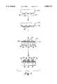
- FIG. 1illustrates schematically a process of microcontact printing of a chemical activating agent at defined regions of a substrate, followed by deposition of metal at the defined regions;
- FIGS. 2a, 2b and 2care photocopies of scanning electron micrograph (SEM) images of micrometallic structures fabricated on substrates in accordance with the invention
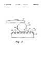
- FIG. 3illustrates schematically the application of an activating agent from an article having a patterned, contoured surface to a nonplanar surface of an article
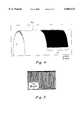
- FIG. 4is a photocopy of a photograph of a glass article having a non-planar surface including a region patterned with copper after microcontact printing of a chemical activating agent;
- FIG. 5is a photocopy of an optical micrograph of the copper pattern on the curved substrate of FIG. 4;
- FIG. 6ais a photocopy of an SEM image of a free-standing metal microstructure removed from a substrate to which it had been deposited after application of a chemical activating agent to the substrate;
- FIG. 6bis a photocopy of the structure of FIG. 6a at higher magnification.
- FIGS. 7a and 7bare photocopies of atomic force microscopy (AFM) images of a grid of lines of metal deposited in accordance with the present invention.
- AFMatomic force microscopy
- the present inventionprovides a strategy for applying to a surface a chemical activating agent, such as a catalyst, quickly, cleanly, and efficiently.
- the inventioninvolves metal plating on a substrate by direct application onto the substrate of an activating agent that promotes deposition of the metal followed by deposition of the metal on the substrate.
- an activating agentthat promotes deposition of the metal followed by deposition of the metal on the substrate.
- Edge resolutionis meant to define that an intended linear portion of a patterned metal feature will deviate from a straight line in an amount less than or equal to about 100 nm.
- Devices fabricated in accordance with the inventioncan be used for a variety of purposes that will be apparent to those of ordinary skill in the art, for example microelectronics, optics, antennas, and the like.
- FIG. 1is a schematic illustration of a method of depositing a metal on a substrate surface.
- an applicatorin particular a stamp 20
- a surface 22 including indentations 24 formed therein and defining an indentation patternthe indentations contiguous with an application surface 26 defining an application pattern.
- surface 22includes protrusions 26, each having an outward-facing surface defining an application pattern.
- indentations 24may be interconnected to form a single, continuous, patterned indentation and/or protrusions 26 may be interconnected to form a single, continuous, patterned protrusion.
- protrusions 26may define a patterned application surface, including a plurality of application regions isolated by an intervening indentation(s), or a patterned stamping surface that is a single, continuous region contiguous with a continuous indentation or indentations.
- the inventionprovides for deposition of metal on a substrate surface in a manner such that the metal so formed has a lateral dimension, or dimension parallel to the substrate surface (width) of less than about 1 mm.
- thisis achieved by providing a stamp 20 having a protrusion, or stamping surface 26, having a lateral dimension, or dimension generally parallel to surface 22, of less than about 1 mm.
- the lateral dimension of protrusion or stamping surface 26is less than about 500 mm or 100 mm, more preferably less than about 50 mm, 20 mm, or 10 mm, most preferably less than about 5 mm or 1 mm.
- the inventionprovides for essentially instantaneous transfer, to a region of a substrate surface having an area of at least ten square microns, a chemical activating agent.
- the activating agentcan be in collidal form.
- the activating agentis applied essentially instantaneously to a region of the substrate surface having an area of at least about 50 square microns, preferably, at least about 100 square microns, more preferably, at least about 200 or about 500 square microns, and most preferably, at least about 1,000 square microns.
- the inventioninvolves essentially instantaneous transfer of a chemical activating agent to a substrate surface in an area of less than about ten square microns, preferably less than about five square microns, more preferably less than about two square microns and most preferably, less than about one square micron.
- an applicator including a plurality of protrusionsFor purposes of illustration, a preferred embodiment of an applicator including a plurality of protrusions is described and illustrated. It is to be understood, however, that any applicator that is capable of carrying a chemical activating agent and transferring the chemical activating agent to a substrate surface finds use in the invention.
- a flat applicator to which a pattern of a chemical activating agent is applied(for example using techniques as described in the present invention or other techniques) can be used to transfer the chemical activating agent, in the pattern, to a substrate surface.
- the shapes of the protrusions described and illustratedneed not be of essentially rectangular cross section, but can be of any shape.
- protrusions having more pointed featuressuch as those molded in anisotropically-etched molds as described in co-pending, commonly owned U.S. application Ser. No. 08/397,635, incorporated herein by reference, may be used to form particularly fine features on a substrate surface.
- FIG. 1will be further described, for purposes of example only, in terms of a metal deposition or plating reaction using a stamp as an applicator.
- an activating agent 28 that promotes deposition of a metalis applied to surface 22, notably application or stamping surface 26.
- Stamp 20is placed in proximity of a substrate 30 that includes a surface 32 facing the stamp.
- the stampis positioned in a first orientation, proximate surface 32, such that activating agent 28 is transferred to regions 34 of surface 32 from stamping surface 26.
- Second portions 36 of surface 32, contiguous with first portions 34remain free of activating agent 28.
- regions 34 of substrate surface 32 that correspond to the stamping pattern 26receive the activating agent.
- the pattern of activating agent 28 applied to surface 32can be a continuous region or can be a plurality of isolated regions.
- an adhesion promoter 38can be applied to surface 32 prior to application of the activating agent 28 thereto, or activating agent 28 can be applied directly to surface 32 in the absence of adhesion promoter 38 under certain circumstances.
- a description of activating agents 28 and substrates 30 amenable to the process of the invention with, and without, adhesion promoteris described more fully below. It is to be understood that, when an adhesion promoter is required, it is needed only at those regions of substrate 30 at which activating agent 28 is to be applied, but can be applied to any region of the surface.
- adhesion promotersuch as a self-assembled monolayer
- description of the invention that involves transfer or application of a chemical activating agent to the surface, or depositing a species on a surfaceis meant to include transfer or deposition on an adhesion promoter that is, in turn, on a surface.
- a metal 40is deposited at regions 34 of surface 30 to which activating agent 28 has been applied, via a reaction effected by the activating agent.
- the metalis formed at surface 30 in the form of a pattern corresponding to the pattern in which activating agent 28 is applied.
- the metalthus can be deposited in the form of isolated regions, or in the form of a single continuous region that, according to one embodiment, is in the form of a pathway delineating a pattern.
- the term "pattern"is meant to define a predetermined, planned shape that can effectively be created on a substrate surface.
- Such a predetermined patterncan include a plurality of isolated, non-interconnected regions such as an array or grid of dots or squares, a single region that includes linear and non-linear portions such as an electronic circuit, or a combination. While a random pattern can be generated, one advantage of the invention is that a pattern can be pre-designed and then created on a surface in accordance with the invention.
- stamp surface 26is removed from the proximity of surface 32, optionally re-coated with activating agent 28, is positioned in a second orientation different from the first stamping orientation, and is again brought into proximity of surface 32 thereby applying activating agent 28 to portions of surface 32 different from and/or in addition to those portions to which agent 28 had been applied during the original application step.
- activating agent 28can be used in the various steps. For example (not shown in FIG.
- a pattern of activating agent 28can first be formed on surface 32 via transfer from stamping surface 26 positioned in a first orientation, the first pattern including at least one essentially linear portion, followed by positioning of stamping surface 26 in a second orientation such that a second linear portion of activating agent 28 is formed that intersects the first essentially linear portion.
- Any other set of first and second orientations of stamp 20, resulting in a variety of patterns of activating agent 28 on surface 32,can be formed.
- a second stamp having a similar or different stamping patterncan be used to transfer a similar or different pattern of activating agent 28 in a similar or different orientation to surface 32 of substrate 30.
- successive transfer of different activating agents to surface 32 from one or more applicators in similar or dissimilar orientationscan take place. The same or different activating agents can be used in the various transfer steps.
- metal 40can be deposited at surface 32 at a region or regions to which activating agent 28 had been applied, forming a pattern corresponding to the pattern of activating agent 28.
- stamp 20Following plating of metal 40 at surface 32, stamp 20, or a different stamp, can be applied to surface 32 in an orientation the same or different from that of the orientation of the first stamping procedure to deposit an activating agent (the same as or different from the original agent) onto at least one portion of deposited metal 40, onto at least one portion of surface 32 not covered by metal 40, or both. Then, a second depositing step can be carried out in which metal is deposited at surface 32 via activating agent 28 and, in the case of autocatalytic deposition, metal 40 can plate at regions where the metal had previously been deposited.
- an activating agentthe same as or different from the original agent
- the techniques of the inventioncan employ any applicator capable of transferring an activating agent to a substrate surface.
- the applicatormay comprise one or more generally aligned fluid outlets fluidly connected to one or more reservoirs of activating agent that, when brought into proximity of the substrate surface, could deliver to the substrate surface the activating agent.
- the applicatoris capable of applying the activating agent essentially instantaneously to the substrate surface. This generally is achieved in an applicator having application regions aligned essentially in a plane and defining an application surface.
- an applicator having a plurality of regions, optionally isolated from each other, that together can be aligned essentially in a plane, and that together can define an application surface carrying a chemical activating agentwould be suitable for applying the activating agent essentially instantaneously to an essentially planar surface.
- the plurality of regions that together define the application surfacecan be made to form a shape corresponding to the shape of a nonplanar substrate surface the applicator is suitable for applying the activating agent to the nonplanar surface essentially instantaneously.
- the inventionprovides for an efficient method of transferring an activating agent to a surface that involves simply applying the activating agent to the surface from an applicator.
- an applicatorhaving a surface that faces the substrate surface and carries the activating agent
- the activating agentcan be transferred essentially instantaneously, i.e. by stamping, to the substrate surface. The need to carry out a chemical reaction at the surface to convert a precursor to an activating agent is avoided.
- the activating agentis selected as one capable of being carried by an applicator, transferred from the applicator to a surface in a form in which it can effect a chemical reaction (such as a metal deposition reaction), and immobilized at the surface with a degree of adhesion and for a period of time sufficient to participate in the desired chemical reaction.
- the activating agentcan be a transition metal such as palladium, a transition metal colloid, or other agent that can be so transferred. Activating agents are discussed in greater detail below.
- Those of ordinary skill in the artcan formulate or modify a surface of an applicator that is used to transfer an activating agent to a substrate surface, and/or the substrate surface, and/or the activating agent or its carrier, so that transfer from the applicator to the substrate surface can be easily carried out.
- adhesion promoter 38promotes adhesion of activating agent 28 to surface 32 of substrate 30.
- any adhesion promoter that increases the interaction between the activating agent 28 and surface 32is suitable, and its selection will depend somewhat upon the characteristics of surface 32 and the characteristics of activating agent 28.
- adhesion promoter 38can be formed of a silane layer having a variety of terminal groups such as CH 3 , CN, SH, NH 2 , NHCH 2 CH 2 NH 2 , etc.
- Adhesionalso can be achieved by treatment of the substrate with a self-assembled monolayer (SAM) exposing away from the substrate surface a chemical functionality conducive to activating agent adhesion.
- SAM-forming speciesin connection with a variety of substrates, and exposing away from the substrate surface a variety of chemical functionalities, such as hydrophobic or hydrophilic functionalities, etc, are described in commonly-owned copending U.S. patent application Ser. No. 08/131,841 to Kumar et al., incorporated herein by reference.
- silane functionalizationis a preferred method of adhesion promotion.
- Amine-functionalization of a surfacealso can promote adhesion, and surfactants also can be adhesion promoters.
- Oxidizing a surfacealso will promote adhesion to a reasonable extent and this technique, without the use of any adhesion promoter, will be suitable for preparing a surface to receive many activating agents.
- Many surfacesfor example a silicon wafer with a native oxide layer, exhibit good adhesion without use of an adhesion promoter.
- Substrate 30can be an electrical conductor, non-conductor, or semiconductor and can be made of glass, silicon (including a native oxide layer), a polymer, ceramic, or the like. Any substrate can be used that is capable of adhering an active agent 28 to the extent that the active agent can participate in a reaction proximate the substrate surface and, as discussed, the nature of substrate 30 and the nature of activating agent 28 will dictate to some extent the need for, and characteristics of, an adhesion promoter 38.
- a single admixture of adhesion promoter and activating agent 28can be applied to stamping surface 26 and the admixture applied to regions 34 of surface 32 of substrate 30, followed by plating of metal 40 at regions 34.
- the stampcan be made of any material including a stamping surface 26 that can carry activating agent 28 and transfer activating agent 28 to substrate surface 32. Accordingly, the chemical nature of stamping surface 26, activating agent 28, and/or any carrier of activating agent 28 can be together selected such that the activating agent can be effectively transferred from surface 26 to surface 32, as discussed above. Where the chemical nature desired in the stamping surface results in inconvenience or excess expense in the fabrication of the entire stamp from that material, the stamp can be fabricated from any material, and coated at stamping, or application surface 26 with a suitable material. Stamp 20 can be rigid or flexible and, according to a preferred embodiment, stamp 20 is an elastomer such as is described in U.S. patent application Ser. No.
- stamping surfacecan be used to "write" on a surface, as described in application Ser. No. 08/485,457.
- writeis meant to define contacting substrate surface 32 with stamping surface 26 and moving stamping surface 26 laterally relative to substrate surface 32 to apply activating species 28 to surface 32 in a pattern corresponding to movement of the stamp, and in particular application surface 26, relative to surface 32.
- the dimensions of the regions 34 of substrate 32 to which activating agent 28 is appliedcan be altered by, as described in application Ser. No. 08/485,457, referenced above, deforming the stamp prior to and/or during transfer of the activating agent to the substrate surface.
- the stampcan be deformed by compression along any of its axes relative to the substrate, for example compression laterally (in a direction parallel to the substrate), and/or vertically (in a direction parallel to the substrate surface). Such deformation can increase or decrease the lateral dimensions of regions 34 to which activating agent 28 is applied.
- FIG. 2aillustrates a series of copper features (light regions) deposited onto a glass substrate (dark background) following application of a palladium colloidal activating agent to the glass substrate using a stamp in accordance with the invention having a stamping, or application surface 26 (with reference to FIG. 1) corresponding to the pattern of deposited metal shown.
- Copper lines with a width, that is, a dimension parallel to the surface of the substrate, of between about 0.5 micron and 1.5 micronsare shown.
- FIG. 2bis a photocopy of an SEM image of a polyimide substrate (dark background) similarly patterned with deposited copper (light lines) following application of a palladium colloidal activating agent to the substrate via a stamp.
- FIG. 2cis a photocopy of an SEM image of copper deposited on polyimide, as described above, followed by annealing with a propane flame for about 3 seconds.
- the fracture profile of the copper lineshows edge resolution of about 100 nm.
- good edge resolutionis achieved via the methods of the invention and deposition of metals at surfaces of substrates can be carried out so as to result in metal features having an essentially rectangular cross-section, with relatively sharp features. Addition of tensides to a solution from which a metal is plated can assist in formation of an essentially rectangular cross-sectional metal structure.
- an article 42 that has a nonplanar surface 44is shown during a process of transferring to nonplanar surface 44 a pattern of activating agent 28.
- An applicator 46is provided that has a application surface 48 including indentations 50 that are contiguous with application surface 48.
- Application surface 48thus defines a pattern that can be a continuous region including portions isolated by intervening portions of indentation(s) 50, or can be a plurality of separate regions isolated from each other by indentation(s) 50.
- the application surface 48(along with indentations 50, typically) is coated with activating agent 28.
- Article 42is caused to roll over application surface 48, for example by placing article 42 between stamping surface 48 and a member 52 and moving applicator 46 and member 52 relative to each other along parallel planes in opposite directions.
- Member 52can be made of any material that will not disrupt or contaminate surface 44 unacceptably, and preferably a material that will not disrupt activating agent 28 formed on surface 44 to the extent that activating 28 loses its ability to facilitate deposition of metal at surface 44.
- the term "roll”refers to action in which a first surface is maintained in constant contact with a second surface (for example, surface 44 of article 42 and application surface 48, respectively), but only a portion of each surface is in contact with only a portion of the other surface at any given time, and the portion of each surface that is in contact with the portion of the other surface changes continuously.
- article 42is illustrated after having been rotated through approximately 80° of rotation on application surface 48.
- a pattern of activating agent 28 on a surface 44 of article 42is formed around approximately 80° of the surface.
- article 42can be rolled relative to applicator 46 through any desired degree of rotation to form a pattern as desired.
- a metalcan be deposited at regions at which activating agent 28 is deposited.
- FIG. 4a photocopy of a photograph of a glass article 54 having a radius of curvature of approximately 1.25 centimeters is shown.
- a region 56 of the surface of the articlewas patterned with a palladium colloidal activating agent using the technique described above in connection with FIG. 3, followed by electroless deposition of copper.
- FIG. 5is a photocopy of an optical micrograph of a portion of patterned region 56 of FIG. 4, showing resolution of metal features on the nonplanar substrate similar to those achieved on planar substrates as described and shown above.
- articles having a variety of radii of curvaturecan be patterned.
- a wide variety of articles including, for example, optical fibers,can be patterned in accordance with the invention.
- patterns of chemically active agentcan be printed on non-planar articles, at the micron range, the articles having radii of curvature of less than about one centimeter, preferably less than abpit one millimeter, more preferably less than about 500 microns, more preferably less than about 100 microns, more preferably less than about 50 microns, and according to a particularly preferred embodiment printing can occur on substrates with radii of curvature on the order of about 25 microns or less.
- FIG. 6ais a photocopy of an SEM image of a free-standing copper structure made by first applying to a glass substrate a palladium colloidal activating agent using a stamp having a patterned stamping surface, followed by electroless deposition of copper at regions of the surface carrying the activating agent, followed by dissolution of the glass in a dilute aqueous solution of HF.
- the resulting flexible, free-standing, metallic structurehas a pattern corresponding to the pattern of the stamping surface of the stamp.
- FIG. 6bis a photocopy of the SEM image of FIG. 6a at higher resolution.
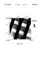
- FIG. 7ais a top view of an atomic force microscopy (AFM) image
- FIG. 7bis a side view AFM image of a grid of 10 micron lines produced by a double stamping technique.
- a stamp having a stamping pattern defined by linear regions interspersed by indentationswas coated with an activating agent, positioned in a first orientation and brought into contact with a substrate and removed, and the substrate subjected to metal deposition. Deposition occurred at regions 58, corresponding to regions to which the activating agent was applied.
- the stampwas oriented above the substrate in a 90° rotation, parallel to the surface, relative to the first orientation and reapplied to the substrate.
- the substratethen was subjected to further metal deposition, resulting in deposition at regions 60 corresponding to the second stamping application of activating agent.
- Regions 62representing regions to which activating agent was applied during the first stamping procedure but to which activating agent was not applied during the second stamping procedure show the greatest amount of metal deposition. This is because the autocatalytic nature of the deposition of copper is favored over deposition of copper initiated by the activating agent.
- the activating agentis selected as one capable of being carried by an applicator, transferred from the applicator to a surface in a form in which it can effect a chemical reaction (such as a metal deposition reaction), and immobilized at the surface with a degree of adhesion and for a period of time sufficient to participate in the desired chemical reaction.
- a chemical reactionsuch as a metal deposition reaction
- one class of activating agents provided in accordance with the inventionare distinguished from prior art agents applied with an applicator such as a stamp, for example as disclosed by Lando (U.S. Pat. Nos. 3,873,359, 3,873,360, and 3,900,614), in that the activating agent of the present invention is in a form suitable for effecting reaction such as metal plating or catalytic action when transferred to the surface.
- further chemical reaction at the surface to convert a precursor to a suitable agentis not required.
- Metal deposition reactions contemplatedinclude electrochemical deposition and electroless deposition, generally involving reduction of a metal cation to create the metal, facilitated in part by the lowering of the electrochemical potential involved in the deposition.
- Activating agents that are finely distributed metal particles and clusterssuch as conventional metal powders, including substrate-fixed metal clusters or multimetallic clusters are suitable for use as activating agents in accordance with the invention, and are well known as valuable heterogeneous and homogeneous catalysts in organic, inorganic, and electrochemistry.
- exemplary activating agentsinclude one or more metals of periodic table groups Ib, IIb, III, IV, V, VI, Vllb, VIII, lanthanides, and actinides, preferably copper and any metal more noble than copper, in particular Pd, Au, Ag, Pt, and Cu.
- Hydrogenation catalystsfor example those effective in hydrogenating olefins or aromatics, as in the partial hydrogenation of benzene to form cyclohexene, with a substrate-fixed ruthenium activating agent or bimetallic activating agent (e.g. Ru/Sn) are contemplated.
- ruthenium activating agent or bimetallic activating agente.g. Ru/Sn
- Zirconium and titanium catalystsare suitable for use in the invention that catalyze polymerization, such as polymerization of olefins such as ethylene, and these are intended to form part of the invention.
- Other examples of catalytic activating agentsinclude those used in Heck reactions, e.g. in the Pd-catalyzed reaction of bromobenzene and styrene to form stilbene.
- Activating agents that are heterogeneous catalystsare also useful as electrocatalysts in fuel cells (in particular substrate-fixed Pt and Pt/Ru clusters).
- Activating agents prepared according to the inventioncan be homogeneous catalysts, such as those used in two phase systems (for instance H 2 O/toluene), such as e.g. betaine-stabilized Pd clusters soluble in H 2 0.
- Activating agents that are embedded in polymerscan be used to prepare materials for electronic, optical and magnetic applications.
- Suitable embedding polymersinclude organic polymers, such as poly-p-phenylene-vinylene, polymethyl methacrylate, polysilanes, and polystyrene, or inorganic polymers, such as zeolites, silicates, and metal oxides.
- organic polymerssuch as poly-p-phenylene-vinylene, polymethyl methacrylate, polysilanes, and polystyrene
- inorganic polymerssuch as zeolites, silicates, and metal oxides.
- solgel processcan be used to incorporate metal clusters in amorphous metal oxide materials (e.g. SiO 2 ) as activating agents.
- Soluble metal clusters that are activating agentscan also be surface-deposited to prepare novel materials for applications in optics and electronics, e.g. Pd on HOPG (highly oriented pyrolytic graphite).
- HOPGhighly oriented pyrolytic graphite
- Particulate activating agents having particle sizes on the order of nanometersare preferred, for example particulate matter having particle size of less than about 100 nm, preferably less than about 50 nm, more preferably less than about 25 nm, and most preferably from about 2 to about 20 nm.
- the size of the particlesis not critical except to the extent that where excellent edge resolution of a structure deposited in a reaction involving the particle is desired, the upper limit in size of the particle is reduced.
- colloidal activating agentsare colloidal activating agents.
- colloidal activating agentis meant to define particulate matter capable of being involved in a desired chemical reaction, such as a catalytic reaction and including plating of metal at surfaces, that is carried or surrounded by molecules that prevent agglomeration of the individual particles and that render the particulate soluble in, or at least able to be carried in, an organic or aqueous liquid.
- a desired chemical reactionsuch as a catalytic reaction and including plating of metal at surfaces
- Suitable colloid-forming species and colloidsare described in European patent publication no. 672765 by Reetz et al., published Sep. 20, 1995, and incorporated herein by reference.
- the activating agentcomprises one or more metals of groups Ib, IIb, III, IV, V, VI, Vllb, VIII, lanthanides, and/or actinides of the periodic table prepared by cathodic reduction in the presence of a stabilizer.
- One method of preparation of such colloidsis reduction, optionally with a supporting electrolyte, in organic solvents or in solvent mixtures of organic solvents and/or water within a temperature range of between about -78° C. and about 120° C. to form metal colloidal solutions or redispersible metal colloid powders, optionally in the presence of inert substrates and/or soluble metal salts of the respective metals.
- colloidsare soluble or redispersible in a suitable fluid that facilitates their application to an applicator such as a stamp.
- an applicatorsuch as a stamp.
- Vargo, et al."Adhesive Electroless Metallization of Fluoropolymeric Substrates” Science, 262, 1711-1712 (Dec. 10, 1993); Bonnemann, et al., “Preparation and Catalytic Properties of NR 4 + Stabilized Palladium Colloids", Applied Organometallic Chemistry 8, 361-378 (1994); Reetz, et al., “Size-Selective Synthesis of Nanostructured Transition Metal Clusters” J. Am. Chem. Soc.
- Electrochemical methodsare described in EP 672765, referenced above, for synthesis of soluble metal colloids by operating in an inert organic, aprotic solvent, with surface-active colloid stabilizers being added as the supporting electrolyte which will both prevent plating of the metal and protect, or stabilize, small metal nuclei in the cluster stage.
- a metal sheetserves as the anode to be dissolved and a metal or glassy carbon electrode serves as the cathode. After dissolution at the anode, the released metal salts are reduced again at the cathode, with tetraalkylammonium salts serving as stabilizers. Standard organic solvents can be employed.
- Suitable exemplary stabilizers, or carriers, for the colloids, and at the same time as the supporting electrolyte,are quaternary ammonium or phosphonium salts R 1 R 2 R 3 R 4 N + X - and R 1 R 2 R 3 R 4 P + X - , respectively.
- R 1 , R 2 , R 3 and R 4are possible.
- Aryltrialkylammonium saltsmay also be used.
- Suitable counter ionsinclude various anions, e.g.
- halogenidesCl - , Br - , I -
- PF 6 -hexafluorophosphate
- phosphonium saltsincluding tetraarylphosphonium salts, such as tetraphenylphosphonium bromide.
- tetrabutylammonium chloridebromide or hexafluorophosphate, tetraoctylammonium bromide, or tributylhexadecylphosphonium bromide
- metalsany of those listed above, in particular transition metals such as Fe, Co, Ni, Pd, Pt, Ir, Rh, Cu, Ag, or Au, are suitable.
- Suitable solventsare aprotic organic solvents, such as tetrahydrofuran (THF), toluene, acetonitrile (ACN), or mixtures thereof.
- the temperature in the electrolytic cellmay be in the range between -78° C. and +120° C., preferably 15-30° C. or room temperature.
- metal colloids of various metals and metal alloys having various sizes and being stabilized by quaternary ammonium or phosphonium saltscan be synthesized for use as activating agents in accordance with the invention.
- the size of the metal colloidsis determined by varying the current density which immediately affects the reduction potential of the cathode. The higher the overvoltage, which is defined as the deviation of the reduction potential from the equilibrium potential, the smaller the maximum size of the metal nuclei in the electrolytic boundary layer. Nuclei are trapped since the surface-active agents used as supporting electrolytes form a surrounding protective shell that prevents further growth. Thus, the size of the metal colloids can be controlled.
- soluble Pd colloids stabilized by tetraoctylammonium bromidecan be prepared with selected diameters of about 2 nm, 5 nm, or 10 nm, depending on the current density applied, i.e. 3.4, 1 and 0.4 mA/cm 2 , respectively, at the same concentration of the stabilizer.
- R 4 N + X - stabilized metal colloidscan be formed in accordance with this embodiment of the invention with the use of solubilized metal stock or metal salts.
- RCH 3 , CF 3 , CH 3 C 6 H 4 ), and of acetylacetonates.
- Mrepresents according to this technique main group elements, for instance Ga, In or TI, as well as transition metals, for instance Fe, Co, Ni, Cu, Mo, Ru, Rh, Pd, Ag, Os, Pt, or Au.
- transition metalsfor instance Fe, Co, Ni, Cu, Mo, Ru, Rh, Pd, Ag, Os, Pt, or Au.
- the above-mentioned ammonium or phosphonium saltsserve as stabilizers for the colloids.
- Solventssuch as those mentioned above, for example THF, toluene, propylene carbonate, acetonitrile, or mixtures thereof as well as mixtures of THF and H 2 O or of ACN and H 2 O, serve as solvents.
- THF and alcoholssuch as methanol or ethanol, or of ACN and alcohols may also be used.
- the temperature in the electrolytic cellmay be within the above-mentioned range.
- inert electrode materialsconventionally used in electrochemistry, e.g. Pt sheets or graphite, can be used.
- water solubilitycan be achieved by using ionic (cationic, anionic, zwitterionic) or nonionic stabilizers which are readily soluble in water, optionally in the presence of a supporting electrolyte, e.g. lithium chloride, lithium acetate, or tetramethylammonium acetate.
- ioniccationic, anionic, zwitterionic
- nonionic stabilizerswhich are readily soluble in water, optionally in the presence of a supporting electrolyte, e.g. lithium chloride, lithium acetate, or tetramethylammonium acetate.
- Anionic stabilizersinclude e.g. alkali metal salts of amino acid derivatives, such as e.g. sodium alkylamido-N-hydroxyethyl-glycinates or succinates.
- Suitable zwitterionic stabilizersinclude e.g.
- Suitable non-ionic stabilizersinclude e.g. sugar derivatives, such as the commercially available substances of the TWEEN® group, modified cyclodextrines, polyglycosides, octanoyl-N-methylglucamide (MEGA-8), heptylglucopyranoside, poly(vinyl alcohol), and also polyoxyethylene alkyl ethers (BRIJ 35). Variation in size of the colloid can be controlled by varying the current density which immediately affects the reduction potential of the cathode. The higher the overvoltage, the smaller the particle size.
- Multimetallic metal colloidscan be prepared using mixtures of two or more different metal salts, or by using as electrodes a readily dissolved metal anode (sheets of e.g. Al, Ti, Sn, Ni, Cu, Pd, Ag, or Au) and an inert cathode (e.g. a platinum sheet) with addition of a metal salt MX n in a common solvent.
- a readily dissolved metal anodesheets of e.g. Al, Ti, Sn, Ni, Cu, Pd, Ag, or Au
- an inert cathodee.g. a platinum sheet
- the electrochemical processinvolved oxidative dissolution of the anode to form a second metal salt, and both metal salts are concurrently reduced at the cathode to form bimetallic stabilized colloids.
- the water soluble colloids prepared according to the inventioncan be used for the preparation of stable aqueous solutions with metal contents of above 4 mmol of metal per liter. Also possible is the preparation of aqueous solutions acidified with hydrochloric or sulfuric acid such as those used in electroplating and electroforming technology, e.g. in electroless plating (See, for example, O. J. Murphy et al., "Electrochemistry in transition: From the 20 th to the 21 st century", Plenum Press, New York, 1992, page 39, incorporated herein by reference).
- Activating agents suitable for use in the inventionalso include carrier-fixed metal clusters, in which an undoped or doped carrier is covered with a solution in H 2 O of a water soluble colloid, and the water is separated.
- Suitable carriersinclude, e.g., activated charcoal, metal oxides such as TiO 2 , SiO 2 , Al 2 O 3 , MgO, or insoluble organic polymers (for example a polyamide, such as Kevlar®).
- An immobilized metal clusteris thus obtained in a simple manner.
- a slurry of the carrier in an electrolytemay be formed and electrolysis performed in the presence of the carrier.
- the metal clusters generatedare fixed in situ on the carrier.
- Chemically active or biochemically active agents and species and precursors of structuresare suitable for use as species transferred from an applicator to a substrate surface in accordance with the invention as described with respect to activating agents herein.
- the success of the inventionis due in part to control of the chemical and physical relationship between the activating agent, and/or any carrier in which it is provided, and the application surface of the applicator, and between the activating agent and/or carrier and the surface of the substrate to which the activating agent is applied, and in part to stabilization and solubilization of activating agents in suitable solvents.
- the exposed chemical functionality of the activating agentthat is, the chemical nature (e.g., the chemical nature (e.g.
- the degree of polarity, hydrophobicity, hydrophilicity, et al.) of the portion of the activating agent or stabilizer or carrier that comes into contact with its surroundingsshould be selected in conjunction with the chemical functionality of the application surface such that the activating agent will adhere to the application surface to an extent needed for the applicator to carry the activating agent to the substrate surface, but not to an extent that the activating agent will not be readily transferred from the application surface to the substrate surface when the applicator is brought into contact with the substrate. That is, the wetting properties of the stamp should be somewhat matched to the chemical functionality of the activating agent.
- the activating agentshould be selected in conjunction with the substrate such that it will adhere to the substrate to an extent necessary for it to participate in a desired chemical reaction, such as metal plating, at the surface.
- a desired chemical reactionsuch as metal plating
- the selection of material for fabrication of the applicator, at least portions of the applicator defining the application surface,should be carried out with the chemical functionality of the activating agent in mind.
- the substrate, at least that portion which will receive the activating agent,should be similarly selected. In many instances it will be desirable to use a particular material for a substrate, and a particular activating agent, and the chemical nature of the activating agent will not be particularly suited for adhesion at the substrate, or suited for transport from the application surface to the substrate surface.
- an ionic, nonionic, or zwitterionic surfactant or other surface-active agentsuch as a fluorocarbon, perfluoropolyacrylate, silicone, siloxane such as dimethoxypolysiloxane, diol such as 2, 4, 7, 9-tetramethyl-5-decyn-4,7-diol, diol obtained by reacting ethylene oxide with acetylenic glyco, 2, 4, 7, 9-tetramethyl-5-decyne-4, 7 diol, and the like can be used to stabilize or carry the particle.
- an ionic, nonionic, or zwitterionic surfactant or other surface-active agentsuch as a fluorocarbon, perfluoropolyacrylate, silicone, siloxane such as dimethoxypolysiloxane, diol such as 2, 4, 7, 9-tetramethyl-5-decyn-4,7-diol, diol obtained by reacting ethylene oxide with acety
- Glass, silicon, and polystyrene substrateswere selected for application of an active agent and subsequent deposition of metal in accordance with the invention.
- Silicon substrateswere n-type semiconductor grade silicon ⁇ 100> wafers (2 inch diameter) from Silicon Sense Inc. They were immersed immediately before use in a freshly prepared "piranha” solution for 30 min. The substrates then were rinsed thoroughly with deionized H 2 O and dried under a stream of nitrogen.
- PolystyrenePolystyrene (2 mm thick sheets, crystalline) and polyethylene (0.5 mm thick sheets; Goodfellow) were oxidized by soaking in CrO 3 /H 2 SO 4 for 1 min. The oxidized substrates were rinsed thoroughly with deionized H 2 O and dried under a stream of nitrogen.
- Polyvinylidene chloridePolyvinylidene chloride (Saran Wrap, Dow Chemical) was treated with a low-power, radio-frequency oxygen plasma in a Harrick plasma cleaner (Model PDC-23G) for 5 min at a oxygen pressure of 30 mbar.
- the substrateswere immersed in a solution of organosilanes (50 mM) in heptane, as an adhesion promoter, for 1 hour. After rinsing with heptane and drying under a stream of nitrogen, the substrates were used for the procedure described below for application of active agent followed by metal deposition. Only freshly prepared substrates were used.
- An active agentin particular a palladium colloidal active agent was prepared.
- Tetraoctadecylammonium bromide-stabilized palladium colloidPd/[C 18 H 37 ] 4 N + Br -
- Palladium(II) acetateFluka, 4 g, 17.8 mmol
- tetraoctadecylammonium bromideFluka, 5 g, 4.5 mmol
- the solventswere THF for the synthesis of (Pd/[C 4 H 9 ]N + Br - ) and (Pd/[C 8 H 17 ] 4 N + Br - ) and a 1/1 (v/v) mixture of toluene and THF for the synthesis of (Pd/[C 12 H 25 ] y N+Br - ).
- the suspensions of colloidal palladium(Pd/[C 18 H 37 ] 4 N + Br - ) were prepared by dissolution of 0.3 g of the powder in 200 mL of toluene and sonication in an ultrasound bath for 5 min.
- (Pd/[C 4 H 9 ] 4 N + Br - )was soluble in DMF, (Pd/[C 8 H 17 ] 4 N + Br - ) in THF and (Pd/[C 12 H 25 ] 4 N + Br - ) in toluene.
- the brown solutionswere stable and active for months while in solution and could be handled in air.
- An applicator having a contoured surface defined by an application surface and intervening indentationswas prepared.
- the applicatorwas made in the form of a polydimethyl siloxane stamp.
- SylgardTM 184 silicone elastomer, parts "A” and "B” (10/1 by weight, Dow Corning)was mixed in a plastic cup; trapped air was removed under vacuum.
- the mixturewas poured over a master as described by Kumar, et al., Langmuir, 10, 1498-1511 (1994).
- the masterwas held in a polystyrene petri dish and left at room temperature for approximately two hours. It was cured by heating in an oven at 60° C. for approximately two hours.
- the polydimethyl siloxane stamp fabricated as described in Example 4was "linked" with the active agent as described in Example 3 immersing the surface of the stamp including the stamping surface into the colloidal suspension for 2 s, removing it and drying it under a stream of nitrogen. This procedure was repeated two to three times. The stamp then was placed in contact with a pretreated substrate for 15 min.
- Each of the substrates as described in Example 1glass, silicon, polystyrene, polyvinylidene chloride
- the contact timewas only a few seconds, but still long enough to allow the transfer of the colloid onto the substrate (FIGS. 3-5).
- a copper plating bathincluded: solution A containing 3 g of CuSO 4 , 14 g of sodium potassium tartrate (Rochelle salt), and 4 g of NaOH in 100 mL of distilled water, and solution B including an aqueous formaldehyde solution (37.2 wt %). Solutions A and B were mixed in a 10/1 (v/v) ratio just before the bath was used. To deposit copper, the patterned substrate was immersed into the mixture for 30 s-600 s at room temperature. The plating time to achieve a certain film thickness depended on the age of the plating bath and the type of the substrate. The plating process could be stopped by removing the sample and rinsing it with distilled water.
- the articles resulting from the procedures described in the above examplesincluded a substrate (glass, polymer, or silicon) including a copper pathway delineating a pattern on one region of the substrate, another region of the substrate remaining free of copper.
- the patternsincluded continuous, essentially linear portions of metal having dimensions parallel to the substrate, as illustrated in FIGS. 2a-c, 5, and 6b, of the dimensions described above that can be achieved in accordance with the invention, in particular less than about 1 micron in some cases.
Landscapes
- Engineering & Computer Science (AREA)
- Chemical & Material Sciences (AREA)
- Nanotechnology (AREA)
- Physics & Mathematics (AREA)
- General Physics & Mathematics (AREA)
- Crystallography & Structural Chemistry (AREA)
- Materials Engineering (AREA)
- Condensed Matter Physics & Semiconductors (AREA)
- Manufacturing & Machinery (AREA)
- Composite Materials (AREA)
- Mathematical Physics (AREA)
- Theoretical Computer Science (AREA)
- Microelectronics & Electronic Packaging (AREA)
- General Chemical & Material Sciences (AREA)
- Chemical Kinetics & Catalysis (AREA)
- Mechanical Engineering (AREA)
- Metallurgy (AREA)
- Organic Chemistry (AREA)
- Chemically Coating (AREA)
Abstract
Description
Claims (68)
Priority Applications (3)
| Application Number | Priority Date | Filing Date | Title |
|---|---|---|---|
| US08/616,692US6060121A (en) | 1996-03-15 | 1996-03-15 | Microcontact printing of catalytic colloids |
| PCT/US1997/004237WO1997034025A1 (en) | 1996-03-15 | 1997-03-14 | Microcontact printing of catalytic colloids |
| AU25324/97AAU2532497A (en) | 1996-03-15 | 1997-03-14 | Microcontact printing of catalytic colloids |
Applications Claiming Priority (1)
| Application Number | Priority Date | Filing Date | Title |
|---|---|---|---|
| US08/616,692US6060121A (en) | 1996-03-15 | 1996-03-15 | Microcontact printing of catalytic colloids |
Publications (1)
| Publication Number | Publication Date |
|---|---|
| US6060121Atrue US6060121A (en) | 2000-05-09 |
Family
ID=24470582
Family Applications (1)
| Application Number | Title | Priority Date | Filing Date |
|---|---|---|---|
| US08/616,692Expired - LifetimeUS6060121A (en) | 1996-03-15 | 1996-03-15 | Microcontact printing of catalytic colloids |
Country Status (3)
| Country | Link |
|---|---|
| US (1) | US6060121A (en) |
| AU (1) | AU2532497A (en) |
| WO (1) | WO1997034025A1 (en) |
Cited By (62)
| Publication number | Priority date | Publication date | Assignee | Title |
|---|---|---|---|---|
| US6403397B1 (en) | 2000-06-28 | 2002-06-11 | Agere Systems Guardian Corp. | Process for fabricating organic semiconductor device involving selective patterning |
| US20020117659A1 (en)* | 2000-12-11 | 2002-08-29 | Lieber Charles M. | Nanosensors |
| US20020119251A1 (en)* | 2001-02-23 | 2002-08-29 | Chen William T. | Method and apparatus for forming a metallic feature on a substrate |
| US6444254B1 (en)* | 2000-03-03 | 2002-09-03 | Duke University | Microstamping activated polymer surfaces |
| US20020130311A1 (en)* | 2000-08-22 | 2002-09-19 | Lieber Charles M. | Doped elongated semiconductors, growing such semiconductors, devices including such semiconductors and fabricating such devices |
| WO2003002710A2 (en) | 2001-06-29 | 2003-01-09 | The Board Of Trustees Of Leland Stanford Jr. University | Artificial synapse chip interface for electronic prosthetic retina |
| US6531983B1 (en)* | 1999-07-16 | 2003-03-11 | Mitsubishi Materials Corporation | Method for antenna assembly and an antenna assembly with a conductive film formed on convex portions |
| WO2002056650A3 (en)* | 2001-01-16 | 2003-03-13 | Yissum Res Dev Co | Forming a conducor circuit on a substrate |
| US20030059537A1 (en)* | 2000-03-03 | 2003-03-27 | Ashutosh Chilkoti | Microstamping activated polymer surfaces |
| US20030089899A1 (en)* | 2000-08-22 | 2003-05-15 | Lieber Charles M. | Nanoscale wires and related devices |
| US20030132121A1 (en)* | 2001-11-29 | 2003-07-17 | International Business Machines Corporation | Materials and methods for immobilization of catalysts on surfaces and for selective electroless metallization |
| US6599824B1 (en)* | 2001-02-26 | 2003-07-29 | Advanced Micro Devices, Inc. | System for and method of forming local interconnect using microcontact printing |
| US20030168639A1 (en)* | 2001-12-29 | 2003-09-11 | Cheon Jin Woo | Metallic nanoparticle cluster ink and method for forming metal pattern using the same |
| US6623803B1 (en) | 2000-11-14 | 2003-09-23 | Advanced Micro Devices, Inc. | Copper interconnect stamping |
| US20030213382A1 (en)* | 2002-01-11 | 2003-11-20 | Massachusetts Institute Of Technology | Microcontact printing |
| US20030235930A1 (en)* | 2002-06-25 | 2003-12-25 | Lucent Technologies Inc. | Multi-impression nanofeature production |
| US20040003734A1 (en)* | 2002-07-02 | 2004-01-08 | Shively J. Thomas | Method and apparatus for printing using an electrically conductive ink |
| US20040058067A1 (en)* | 2002-09-19 | 2004-03-25 | Law Kam S. | Method and apparatus for metallization of large area substrates |
| US6770721B1 (en) | 2000-11-02 | 2004-08-03 | Surface Logix, Inc. | Polymer gel contact masks and methods and molds for making same |
| US6776864B2 (en)* | 2001-08-04 | 2004-08-17 | Postech Foundation | Process-for forming metal micro-patterns on plastic substrate |
| US6798464B2 (en) | 2001-05-11 | 2004-09-28 | International Business Machines Corporation | Liquid crystal display |
| US20050064158A1 (en)* | 2003-09-19 | 2005-03-24 | Hyungsoo Choi | Nanostructures including a metal |
| US20050120902A1 (en)* | 2001-04-25 | 2005-06-09 | David Adams | Edge transfer lithography |
| US20060006580A1 (en)* | 2002-08-27 | 2006-01-12 | Obducat Ab | Device for transferring a pattern to an object |
| US20060046203A1 (en)* | 2004-08-31 | 2006-03-02 | Lin-En Chou | Method for producing a thin film transistor and a device of the same |
| US20060116741A1 (en)* | 2001-06-29 | 2006-06-01 | Palanker Daniel V | Optically controlled microfluidic chip |
| US20060169160A1 (en)* | 2005-01-28 | 2006-08-03 | Pavel Kornilovich | Method of forming a contact printing stamp |
| US20060175601A1 (en)* | 2000-08-22 | 2006-08-10 | President And Fellows Of Harvard College | Nanoscale wires and related devices |
| US20060185540A1 (en)* | 2005-01-28 | 2006-08-24 | Pavel Kornilovich | Method of utilizing a contact printning stamp |
| WO2006119716A1 (en)* | 2005-05-09 | 2006-11-16 | Bvt Technologies A.S. | Nanostructured working electrode of an electrochemical sensor, method of manufacturing thereof and sensor containing this working electrode |
| US20060263580A1 (en)* | 2001-11-29 | 2006-11-23 | International Business Machines Corp. | Materials and methods for immobilization of catalysts on surfaces and for selective electroless metallization |
| US20070026565A1 (en)* | 2003-03-06 | 2007-02-01 | National Chiao Tung University | Selective area growth carbon nanotubes by metal imprint method |
| CN1301198C (en)* | 2004-09-08 | 2007-02-21 | 吉林大学 | Method of Microcontact Printing Using Colloidal Crystals as Ink |
| JP2007100139A (en)* | 2005-09-30 | 2007-04-19 | Tdk Corp | Method for forming electroless-plated film, and device for forming catalyst pattern |
| EP1793273A1 (en)* | 2005-12-02 | 2007-06-06 | University of Twente | Method of direct microcontact printing of a pattern on a substrate, the substrate obtainable and the use of such substrate |
| US7254151B2 (en) | 2002-07-19 | 2007-08-07 | President & Fellows Of Harvard College | Nanoscale coherent optical components |
| US20070191651A1 (en)* | 2005-02-25 | 2007-08-16 | Vincent Coupard | Process for the preparation of multimetallic catalysts that can be used in reactions for transformation of hydrocarbons |
| US20070264623A1 (en)* | 2004-06-15 | 2007-11-15 | President And Fellows Of Harvard College | Nanosensors |
| US20080008824A1 (en)* | 2006-07-10 | 2008-01-10 | Samsung Electro-Mechanics Co., Ltd. | Method for manufacturing printed circuit board using imprinting |
| US20080014356A1 (en)* | 2006-06-16 | 2008-01-17 | Ilsoon Lee | Selective metal patterns using polyelect rolyte multilayer coatings |
| US20080069957A1 (en)* | 2006-09-15 | 2008-03-20 | Samsung Electro-Mechanics Co., Ltd. | Method of manufacturing metal film pattern forming body |
| US20080191196A1 (en)* | 2005-06-06 | 2008-08-14 | Wei Lu | Nanowire heterostructures |
| US20080206555A1 (en)* | 2003-09-19 | 2008-08-28 | Hyungsoo Choi | Metallic nanostructures |
| US7476523B2 (en) | 2000-08-14 | 2009-01-13 | Surface Logix, Inc. | Method of patterning a surface using a deformable stamp |
| US20090020910A1 (en)* | 2007-02-27 | 2009-01-22 | Stephen Forrest | System and method for depositing thin layers on non-planar substrates by stamping |
| US20090095950A1 (en)* | 2004-12-06 | 2009-04-16 | President And Fellows Of Harvard College | Nanoscale Wire-Based Data Storage |
| US20090224431A1 (en)* | 2005-03-15 | 2009-09-10 | Inmold Biosystems A/S | Transferring materials to polymer surfaces |
| US20100087013A1 (en)* | 2006-06-12 | 2010-04-08 | President And Fellows Of Harvard College | Nanosensors and related technologies |
| US20100152057A1 (en)* | 2006-11-22 | 2010-06-17 | President And Fellows Of Havard College | High-sensitivity nanoscale wire sensors |
| US20100227382A1 (en)* | 2005-05-25 | 2010-09-09 | President And Fellows Of Harvard College | Nanoscale sensors |
| US20110015089A1 (en)* | 2009-07-14 | 2011-01-20 | Colen Chaim Benjoseph | Methods and apparatus for the detection and differentiation of non-sialated proteins from sialated proteins in a fluid sample |
| US7968474B2 (en) | 2006-11-09 | 2011-06-28 | Nanosys, Inc. | Methods for nanowire alignment and deposition |
| US20110165337A1 (en)* | 2007-05-07 | 2011-07-07 | Nanosys, Inc. | Method and system for printing aligned nanowires and other electrical devices |
| US8058640B2 (en) | 2006-09-11 | 2011-11-15 | President And Fellows Of Harvard College | Branched nanoscale wires |
| US8268538B2 (en) | 2004-08-31 | 2012-09-18 | Taiwan Tft Lcd Association | Method for producing a thin film transistor |
| US20120244279A1 (en)* | 2007-10-29 | 2012-09-27 | Sony Corporation | Polarizer, method of manufacturing polarizer and liquid crystal projector |
| US20120288697A1 (en)* | 2011-05-13 | 2012-11-15 | Xerox Corporation | Coating methods using silver nanoparticles |
| DE10240401B4 (en)* | 2001-09-14 | 2013-08-29 | Qimonda Ag | Method of forming structures on a wafer |
| WO2014180723A3 (en)* | 2013-05-07 | 2014-12-31 | Helmholtz-Zentrum Dresden - Rossendorf E. V. | Component having a metal-containing self-organized layer, method for production thereof and use |
| US9297796B2 (en) | 2009-09-24 | 2016-03-29 | President And Fellows Of Harvard College | Bent nanowires and related probing of species |
| US9390951B2 (en) | 2009-05-26 | 2016-07-12 | Sharp Kabushiki Kaisha | Methods and systems for electric field deposition of nanowires and other devices |
| US20230151492A1 (en)* | 2021-11-16 | 2023-05-18 | Science Applications International Corporation | Direct Printing of Catalyst Inks |
Families Citing this family (10)
| Publication number | Priority date | Publication date | Assignee | Title |
|---|---|---|---|---|
| TW539763B (en)* | 1999-06-18 | 2003-07-01 | Ibm | Method for printing a catalyst on substrates for electroless deposition |
| EP2224508B1 (en) | 1999-07-02 | 2016-01-06 | President and Fellows of Harvard College | Method of separating metallic and semiconducting nanoscopic wires |
| AU2006202493B2 (en)* | 1999-07-02 | 2008-05-22 | President And Fellows Of Harvard College | Nanoscopic wire-based devices, arrays, and methods of their manufacture |
| KR100338329B1 (en)* | 2000-02-25 | 2002-05-27 | 백승준 | Method for forming metal line semiconductor |
| EP1736760A3 (en) | 2000-12-11 | 2008-06-18 | President And Fellows Of Harvard College | Nanosensors |
| DE602004014002D1 (en) | 2004-12-10 | 2008-07-03 | Essilor Int | Stamp for applying a motif, method for making a stamp and method for producing an object based on this stamp |
| US7871670B2 (en)* | 2005-08-10 | 2011-01-18 | 3M Innovative Properties Company | Microfabrication using replicated patterned topography and self-assembled monolayers |
| US8764996B2 (en) | 2006-10-18 | 2014-07-01 | 3M Innovative Properties Company | Methods of patterning a material on polymeric substrates |
| US20080095988A1 (en)* | 2006-10-18 | 2008-04-24 | 3M Innovative Properties Company | Methods of patterning a deposit metal on a polymeric substrate |
| US7968804B2 (en) | 2006-12-20 | 2011-06-28 | 3M Innovative Properties Company | Methods of patterning a deposit metal on a substrate |
Citations (20)
| Publication number | Priority date | Publication date | Assignee | Title |
|---|---|---|---|---|
| US3873360A (en)* | 1971-11-26 | 1975-03-25 | Western Electric Co | Method of depositing a metal on a surface of a substrate |
| US3873359A (en)* | 1971-11-26 | 1975-03-25 | Western Electric Co | Method of depositing a metal on a surface of a substrate |
| US3900614A (en)* | 1971-11-26 | 1975-08-19 | Western Electric Co | Method of depositing a metal on a surface of a substrate |
| US4073981A (en)* | 1977-03-11 | 1978-02-14 | Western Electric Company, Inc. | Method of selectively depositing metal on a surface |
| US4098922A (en)* | 1976-06-07 | 1978-07-04 | Western Electric Company, Inc. | Method for depositing a metal on a surface |
| US4100037A (en)* | 1976-03-08 | 1978-07-11 | Western Electric Company, Inc. | Method of depositing a metal on a surface |
| US4192764A (en)* | 1977-11-03 | 1980-03-11 | Western Electric Company, Inc. | Stabilizing composition for a metal deposition process |
| US4322457A (en)* | 1978-01-25 | 1982-03-30 | Western Electric Co., Inc. | Method of selectively depositing a metal on a surface |
| US4472458A (en)* | 1982-01-27 | 1984-09-18 | Bayer Aktiengesellschaft | Process for the production of metallized semiconductors |
| US4508755A (en)* | 1983-03-30 | 1985-04-02 | Northern Telecom Limited | Method of applying a layer of conductive ink |
| US4555414A (en)* | 1983-04-15 | 1985-11-26 | Polyonics Corporation | Process for producing composite product having patterned metal layer |
| US4690715A (en)* | 1982-06-18 | 1987-09-01 | American Telephone And Telegraph Company, At&T Bell Laboratories | Modification of the properties of metals |
| US4728591A (en)* | 1986-03-07 | 1988-03-01 | Trustees Of Boston University | Self-assembled nanometer lithographic masks and templates and method for parallel fabrication of nanometer scale multi-device structures |
| US4802951A (en)* | 1986-03-07 | 1989-02-07 | Trustees Of Boston University | Method for parallel fabrication of nanometer scale multi-device structures |
| US5009965A (en)* | 1974-10-04 | 1991-04-23 | Nathan Feldstein | Colloidal compositions for electroless deposition |
| US5079600A (en)* | 1987-03-06 | 1992-01-07 | Schnur Joel M | High resolution patterning on solid substrates |
| US5087510A (en)* | 1990-03-22 | 1992-02-11 | Monsanto Company | Electrolessly deposited metal holograms |
| EP0672765A1 (en)* | 1994-03-14 | 1995-09-20 | Studiengesellschaft Kohle mbH | Electrochemical reduction of metal salts as a method of preparing highly dispersed metal colloids and substrate fixed metal clusters by electrochemical reduction of metal salts |
| US5512131A (en)* | 1993-10-04 | 1996-04-30 | President And Fellows Of Harvard College | Formation of microstamped patterns on surfaces and derivative articles |
| WO1997007429A1 (en)* | 1995-08-18 | 1997-02-27 | President And Fellows Of Harvard College | Self-assembled monolayer directed patterning of surfaces |
- 1996
- 1996-03-15USUS08/616,692patent/US6060121A/ennot_activeExpired - Lifetime
- 1997
- 1997-03-14AUAU25324/97Apatent/AU2532497A/ennot_activeAbandoned
- 1997-03-14WOPCT/US1997/004237patent/WO1997034025A1/enactiveApplication Filing
Patent Citations (20)
| Publication number | Priority date | Publication date | Assignee | Title |
|---|---|---|---|---|
| US3873359A (en)* | 1971-11-26 | 1975-03-25 | Western Electric Co | Method of depositing a metal on a surface of a substrate |
| US3900614A (en)* | 1971-11-26 | 1975-08-19 | Western Electric Co | Method of depositing a metal on a surface of a substrate |
| US3873360A (en)* | 1971-11-26 | 1975-03-25 | Western Electric Co | Method of depositing a metal on a surface of a substrate |
| US5009965A (en)* | 1974-10-04 | 1991-04-23 | Nathan Feldstein | Colloidal compositions for electroless deposition |
| US4100037A (en)* | 1976-03-08 | 1978-07-11 | Western Electric Company, Inc. | Method of depositing a metal on a surface |
| US4098922A (en)* | 1976-06-07 | 1978-07-04 | Western Electric Company, Inc. | Method for depositing a metal on a surface |
| US4073981A (en)* | 1977-03-11 | 1978-02-14 | Western Electric Company, Inc. | Method of selectively depositing metal on a surface |
| US4192764A (en)* | 1977-11-03 | 1980-03-11 | Western Electric Company, Inc. | Stabilizing composition for a metal deposition process |
| US4322457A (en)* | 1978-01-25 | 1982-03-30 | Western Electric Co., Inc. | Method of selectively depositing a metal on a surface |
| US4472458A (en)* | 1982-01-27 | 1984-09-18 | Bayer Aktiengesellschaft | Process for the production of metallized semiconductors |
| US4690715A (en)* | 1982-06-18 | 1987-09-01 | American Telephone And Telegraph Company, At&T Bell Laboratories | Modification of the properties of metals |
| US4508755A (en)* | 1983-03-30 | 1985-04-02 | Northern Telecom Limited | Method of applying a layer of conductive ink |
| US4555414A (en)* | 1983-04-15 | 1985-11-26 | Polyonics Corporation | Process for producing composite product having patterned metal layer |
| US4802951A (en)* | 1986-03-07 | 1989-02-07 | Trustees Of Boston University | Method for parallel fabrication of nanometer scale multi-device structures |
| US4728591A (en)* | 1986-03-07 | 1988-03-01 | Trustees Of Boston University | Self-assembled nanometer lithographic masks and templates and method for parallel fabrication of nanometer scale multi-device structures |
| US5079600A (en)* | 1987-03-06 | 1992-01-07 | Schnur Joel M | High resolution patterning on solid substrates |
| US5087510A (en)* | 1990-03-22 | 1992-02-11 | Monsanto Company | Electrolessly deposited metal holograms |
| US5512131A (en)* | 1993-10-04 | 1996-04-30 | President And Fellows Of Harvard College | Formation of microstamped patterns on surfaces and derivative articles |
| EP0672765A1 (en)* | 1994-03-14 | 1995-09-20 | Studiengesellschaft Kohle mbH | Electrochemical reduction of metal salts as a method of preparing highly dispersed metal colloids and substrate fixed metal clusters by electrochemical reduction of metal salts |
| WO1997007429A1 (en)* | 1995-08-18 | 1997-02-27 | President And Fellows Of Harvard College | Self-assembled monolayer directed patterning of surfaces |
Non-Patent Citations (78)
| Title |
|---|
| Amit Kumar, Hans A. Biebuyck, and George M. Whitesides, "Patterning Self-Assembled Monolayers: Applications in Material Science", Langmuir, 10, (1994), pp. 1498-1511. (No mo.). |
| Amit Kumar, Hans A. Biebuyck, and George M. Whitesides, Patterning Self Assembled Monolayers: Applications in Material Science , Langmuir, 10, (1994), pp. 1498 1511. (No mo.).* |
| Andre M. T. van der Putten and Jan Willem G. de Bakker, Anisotropic Deposition of Electroless Nickel , J. Electrochem. Soc., vol. 140, No. 8, pp. 2229 2235. Aug. 1993.* |
| Andre M. T. van der Putten and Jan-Willem G. de Bakker, "Anisotropic Deposition of Electroless Nickel", J. Electrochem. Soc., vol. 140, No. 8, pp. 2229-2235. Aug. 1993. |
| Andre M. T. van der Putten, "Controlled Mechanical Adhesion of Electroless Cu Patterns", J. Electrochem. Soc., vol. 140, No. 8, pp. 2376-2378. Aug. 1993. |
| Andre M. T. van der Putten, Controlled Mechanical Adhesion of Electroless Cu Patterns , J. Electrochem. Soc., vol. 140, No. 8, pp. 2376 2378. Aug. 1993.* |
| Andre M.T. van der Putten, Jan Willem G. De Bakker, and Lambertus G.J. Fokkink, Electrochemistry of Colloidal Palladium , J. Electrochem. Soc., vol. 139, No. 12, pp. 3475 3480. Dec. 1992.* |
| Andre M.T. van der Putten, Jan-Willem G. De Bakker, and Lambertus G.J. Fokkink, "Electrochemistry of Colloidal Palladium", J. Electrochem. Soc., vol. 139, No. 12, pp. 3475-3480. Dec. 1992. |
| Cecelia Y. Mak, "Electroless Copper Deposition on Metals and Metal Silicides", MRS Bulletin, pp. 55-62. Aug. 1994. |
| Cecelia Y. Mak, Electroless Copper Deposition on Metals and Metal Silicides , MRS Bulletin, pp. 55 62. Aug. 1994.* |
| Chiu H. Ting and M. Paunovic, Selective Electroless Metal Deposition of Integrated Circuit Fabrication, J. Electrochem. Socl., vol. 136, No. 2, pp. 456 462. Feb. 1989.* |
| Chiu H. Ting and M. Paunovic, Selective Electroless Metal Deposition of Integrated Circuit Fabrication, J. Electrochem. Socl., vol. 136, No. 2, pp. 456-462. Feb. 1989. |
| Christopher B. Gorman, Hans A. Biebuyck, and George M. Whitesides, "Fabrication of Patterned, Electrically Conducting Polypyrrole Using a Self-Assembled Monolayer: A Route to All-Organic Circuits", Chem. Mater. 7, (1995), pp. 526-629. (No. mo.). |
| Christopher B. Gorman, Hans A. Biebuyck, and George M. Whitesides, Fabrication of Patterned, Electrically Conducting Polypyrrole Using a Self Assembled Monolayer: A Route to All Organic Circuits , Chem. Mater. 7, (1995), pp. 526 629. (No. mo.).* |
| David John Pritchard, Hywel Morgan, and Jonathan Mark Cooper, "Micron-Scale Patterning of Biological Molecules", Angew. Chem. Int. Ed. Engl. 34, No. 1 (1995), pp. 91-93. (No mo.). |
| David John Pritchard, Hywel Morgan, and Jonathan Mark Cooper, Micron Scale Patterning of Biological Molecules , Angew. Chem. Int. Ed. Engl. 34, No. 1 (1995), pp. 91 93. (No mo.).* |
| E. Kim et al., "Combining Patterned Self-Assembled Monolayers of Alkanethiolates on Gold with Anisotropic Etching of Silicon to Generate Controlled Surface Morphologies", J. Electrochem. Soc., vol. 142, No. 2, Feb. 1995. |
| E. Kim et al., Combining Patterned Self Assembled Monolayers of Alkanethiolates on Gold with Anisotropic Etching of Silicon to Generate Controlled Surface Morphologies , J. Electrochem. Soc., vol. 142, No. 2, Feb. 1995.* |
| E.A. Dobisz et al., "Self-Assembled Monolayer Films for Nanofabrication", Mat. Res. Soc. Symp. Proc., vol. 380, 1995. (No mo). |
| E.A. Dobisz et al., Self Assembled Monolayer Films for Nanofabrication , Mat. Res. Soc. Symp. Proc., vol. 380, 1995. (No mo).* |
| Enoch Kim, Younan Xia, and George M. Whitesides, "Polymer microstructures formed by moulding in in capillaries", Nature, vol. 376, pp. 581-584. Aug. 1995. |
| Enoch Kim, Younan Xia, and George M. Whitesides, Polymer microstructures formed by moulding in in capillaries , Nature, vol. 376, pp. 581 584. Aug. 1995.* |
| Fiona C. Meldrum, Nicholas A. Kotov, and Janos H. Fendler, "Formation of Thin Films of Platinum, Palladium, and Mixed Platinum: Palladium Nanocrystallites by the Langmuir Monolayer Technique", Chem. Mater. 7, (1995), pp. 1112-1116. (No mo.). |
| Fiona C. Meldrum, Nicholas A. Kotov, and Janos H. Fendler, Formation of Thin Films of Platinum, Palladium, and Mixed Platinum: Palladium Nanocrystallites by the Langmuir Monolayer Technique , Chem. Mater. 7, (1995), pp. 1112 1116. (No mo.).* |
| G.D. Wolf et al., "Neues Verfahren zur ganzflachigen und partiellen Metallisierung von Kunststoffen", Galvanotechnik, vol. 84, No. 7., pp. 2218-2226, 1993. |
| G.D. Wolf et al., Neues Verfahren zur ganzfl a chigen und partiellen Metallisierung von Kunststoffen , Galvanotechnik, vol. 84, No. 7., pp. 2218 2226, 1993.* |
| Genady S. Lazarov, Nikolal D. Kenkov, Orlin D. Veley and Peter A. Kralchevsky, and Kuniaki Nagayama, "Formation of Two-dimensional Structures from Colloidal Particles on Fluorinated Oil Substrate", J. Chem. Soc. Faraday Trans. 90 (14), (1994), pp. 2077-2083, (No mo). |
| Genady S. Lazarov, Nikolal D. Kenkov, Orlin D. Veley and Peter A. Kralchevsky, and Kuniaki Nagayama, Formation of Two dimensional Structures from Colloidal Particles on Fluorinated Oil Substrate , J. Chem. Soc. Faraday Trans. 90 (14), (1994), pp. 2077 2083, (No mo).* |
| Helmut B o nnemann, Rainier Brinkmann and Peter Neiteler, Preparation and Catalytic Properties of NR 4 Stabilized Palladium Colloids , Applied Organometallic Chemistry, vol. 8, (1994), pp. 361 378. (No mo.).* |
| Helmut Bonnemann, Rainier Brinkmann and Peter Neiteler, "Preparation and Catalytic Properties of NR+4-Stabilized Palladium Colloids", Applied Organometallic Chemistry, vol. 8, (1994), pp. 361-378. (No mo.). |
| J.F. Dijksman, "Analysis of the injection-moulding process", Philips tech. Rev. 44, No. 7, pp. 212-217. Mar. 1989. |
| J.F. Dijksman, Analysis of the injection moulding process , Philips tech. Rev. 44, No. 7, pp. 212 217. Mar. 1989.* |
| J.K. Schoer et al., "Scanning Probe Lithography", Langmuir, vol. 10, No. 3, pp. 615-618, 1994. (Abstract) (No mo). |
| J.K. Schoer et al., Scanning Probe Lithography , Langmuir, vol. 10, No. 3, pp. 615 618, 1994. (Abstract) (No mo).* |
| James S.H. Cho, Ho Kyu Kang, S. Simon Wong, and Yosi Shacham Diamand, Electroless Cu for VLSI , MRS Bulletin, pp. 31 37. Jun. 1993.* |
| James S.H. Cho, Ho-Kyu Kang, S. Simon Wong, and Yosi Shacham-Diamand, "Electroless Cu for VLSI", MRS Bulletin, pp. 31-37. Jun. 1993. |
| James W. Wilbur, Amit Kumar, Enoch Kim, and George M. Whitesides, "Microfabrication by Microcontact Printing of Self-Assembled Monolayers", Adv. Mater. 6, No. 7/8 (1994), pp. 600-604, (No mo.). |
| James W. Wilbur, Amit Kumar, Enoch Kim, and George M. Whitesides, Microfabrication by Microcontact Printing of Self Assembled Monolayers , Adv. Mater. 6, No. 7/8 (1994), pp. 600 604, (No mo.).* |
| Jeffrey M. Calvert, Mu San Chen, Charles S. Dulcey, Jackque H. Georger, Martin C. Peckerar, Joel M. Schnur, and Paul E. Schoen, Deep ultraviolet patterning of monolayer films for high resolution lythography , J. Vac. Sci. Technol. B9 (6), pp. 34473450. Dec. 1991.* |
| Jeffrey M. Calvert, Mu-San Chen, Charles S. Dulcey, Jackque H. Georger, Martin C. Peckerar, Joel M. Schnur, and Paul E. Schoen, "Deep ultraviolet patterning of monolayer films for high resolution lythography", J. Vac. Sci. Technol. B9 (6), pp. 34473450. Dec. 1991. |
| Jeffrey W. Jacobs and Stephen P.A. Fodor, "Combinatorial chemistry--applications of light-directed chemical synthesis", Tibtech, vol. 12, pp. 19-26. Jan. 1994. |
| Jeffrey W. Jacobs and Stephen P.A. Fodor, Combinatorial chemistry applications of light directed chemical synthesis , Tibtech, vol. 12, pp. 19 26. Jan. 1994.* |
| Jian Li, Robert Blewer, and J.W. Mayer, "Copper-Based Metallization for ULSI Applications", MRS Bulletin, pp. 18-21. Jun. 1993. |
| Jian Li, Robert Blewer, and J.W. Mayer, Copper Based Metallization for ULSI Applications , MRS Bulletin, pp. 18 21. Jun. 1993.* |
| John E. Shaw, "Capillary fill encapsulation of ISFETs", Sensors and Actuators A, 37-38 (1993), pp. 74-76. |
| John E. Shaw, Capillary fill encapsulation of ISFETs , Sensors and Actuators A, 37 38 (1993), pp. 74 76.* |
| Kuniaki Nagayami, "Fabrication of Two-Dimensional Colloidal Arrays", Phase Transitions, vol. 45, (1993) pp. 185-203 (No mo.). |
| Kuniaki Nagayami, Fabrication of Two Dimensional Colloidal Arrays , Phase Transitions, vol. 45, (1993) pp. 185 203 (No mo.).* |
| Manfred T. Reetz and Wolfgang Helbig, "Size-Selective Synthesis of Nanostructured Transition Metal Clusters", J. Am. Chem. Soc. 116 (1994), pp. 7401-7402. (No mo.). |
| Manfred T. Reetz and Wolfgang Helbig, Size Selective Synthesis of Nanostructured Transition Metal Clusters , J. Am. Chem. Soc. 116 (1994), pp. 7401 7402. (No mo.).* |
| Manfred T. Reetz, Wolfgang Helbig, Stefan A. Quaiser, Ulrich Stimming, Norbert Breuer, and Roland Vogel, "Visualization of Surfactants on Nanostructured Palladium Clusters by a Combination of STM and High-Resolution TEM", Science, vol. 267 (1995), pp. 367-369. No. Mo. |
| Manfred T. Reetz, Wolfgang Helbig, Stefan A. Quaiser, Ulrich Stimming, Norbert Breuer, and Roland Vogel, Visualization of Surfactants on Nanostructured Palladium Clusters by a Combination of STM and High Resolution TEM , Science, vol. 267 (1995), pp. 367 369. No. Mo.* |
| Noo Li Jeon and Ralph G. Nuzzo, Younan Xia, Milan Mrksich, and George M. Whitesides, "Patterned Self-Assembled Monolayers Formed by Microcontact Printing Direct Selective Metalization by Chemical Vapor Deposition on Planar and Nonplanar Substrates", Langmuir, 11, (1995), pp. 3024-3026. (No mo.). |
| Noo Li Jeon and Ralph G. Nuzzo, Younan Xia, Milan Mrksich, and George M. Whitesides, Patterned Self Assembled Monolayers Formed by Microcontact Printing Direct Selective Metalization by Chemical Vapor Deposition on Planar and Nonplanar Substrates , Langmuir, 11, (1995), pp. 3024 3026. (No mo.).* |
| Patrick Hover, Nobuyoshi Baba, and Hideki Masuda, "Small quantum-sized CdS particles assembled to form a regularly nanostructured porous film", Appl. Phys. Lett. 66 (20), pp. 2700-2702. May 1995. |
| Patrick Hover, Nobuyoshi Baba, and Hideki Masuda, Small quantum sized CdS particles assembled to form a regularly nanostructured porous film , Appl. Phys. Lett. 66 (20), pp. 2700 2702. May 1995.* |
| Robert L. Jackson, "Initiation of Electroless Copper Plating Using Pd+2/Poly(acrylic acid) Films", J. Electrochem. Soc., (1988), pp. 3172-3173. (No mo.). |
| Robert L. Jackson, "PD+2/Poly(acrylic acid) Thin Films as Catalysts for Electroless Copper Deposition: Mechanism of Catalyst Formation", J. Electrochem. Soc., vol. 137, No. 1, pp. 95-101. Jan. 1990. |
| Robert L. Jackson, Initiation of Electroless Copper Plating Using Pd 2/Poly(acrylic acid) Films , J. Electrochem. Soc., (1988), pp. 3172 3173. (No mo.).* |
| Robert L. Jackson, PD 2/Poly(acrylic acid) Thin Films as Catalysts for Electroless Copper Deposition: Mechanism of Catalyst Formation , J. Electrochem. Soc., vol. 137, No. 1, pp. 95 101. Jan. 1990.* |
| S. Nakahara and Y. Okinaka, "Microstructure and Mechanical Properties of Electroless Copper Deposits", Annu. Rev. Mater. Sci. 21, (1991), pp. 93-129. (No mo). |
| S. Nakahara and Y. Okinaka, Microstructure and Mechanical Properties of Electroless Copper Deposits , Annu. Rev. Mater. Sci. 21, (1991), pp. 93 129. (No mo).* |
| Stephen J. Potochnik, Pehr E. Pehrsson, David S. Y. Hsu, and Jeffrey M. Calvert, "Selective Copper Chemical Vapor Deposition Using Pd-Activated Organosilane Films", Langmuir, vol. 11, No. 6, (1995), pp. 1841-1845. (No mo.). |
| Stephen J. Potochnik, Pehr E. Pehrsson, David S. Y. Hsu, and Jeffrey M. Calvert, Selective Copper Chemical Vapor Deposition Using Pd Activated Organosilane Films , Langmuir, vol. 11, No. 6, (1995), pp. 1841 1845. (No mo.).* |
| Steven J. Sundberg et al., "Spatially-Addressable Immobilization of Macromolecules on Solid Supports", J. Am. Chem. Soc., vol. 117 (1995), pp. 12050-12057. (No mo.). |
| Steven J. Sundberg et al., Spatially Addressable Immobilization of Macromolecules on Solid Supports , J. Am. Chem. Soc., vol. 117 (1995), pp. 12050 12057. (No mo.).* |
| T.P. Moffat et al., "Patterned Metal Electrodeposition Using an Alkanethiolate Mask", J. Electrochem. Soc., vol. 142, No. 11, Nov. 1995. |
| T.P. Moffat et al., Patterned Metal Electrodeposition Using an Alkanethiolate Mask , J. Electrochem. Soc., vol. 142, No. 11, Nov. 1995.* |
| Terrence G. Vargo, Joseph A. Gardella Jr., Jeffrey M. Calvert, and Mu San Chen, Adhesive Electroless Metallization of Fluoropolymeric Substrates , Science, vol. 262, pp. 1711 1712. Dec. 1993.* |
| Terrence G. Vargo, Joseph A. Gardella Jr., Jeffrey M. Calvert, and Mu-San Chen, "Adhesive Electroless Metallization of Fluoropolymeric Substrates", Science, vol. 262, pp. 1711-1712. Dec. 1993. |
| Valery M. Dubin, "Electroless Ni--P Deposition on Silicon with Pd Activation", J. Electrochem. Soc., vol. 139, No. 5, May, 1992, pp. 1289-1294. |
| Valery M. Dubin, Electroless Ni P Deposition on Silicon with Pd Activation , J. Electrochem. Soc., vol. 139, No. 5, May, 1992, pp. 1289 1294.* |
| Walter J. Dressick and Jeffrey M. Calvert, "Patterning of Self-Assembled Films Using Lithographic Exposure Tools", Jpn. J. Appl. Phys., vol. 32, pp. 5829-5839. Dec. 1993. |
| Walter J. Dressick and Jeffrey M. Calvert, Patterning of Self Assembled Films Using Lithographic Exposure Tools , Jpn. J. Appl. Phys., vol. 32, pp. 5829 5839. Dec. 1993.* |
| Walter J. Dressick, Charles S. Dulcey, Jacque H. Georger, Jr., and Jeffrey M. Calvert, "Photopatterning and Selective Electroless Metallizatoin of Surface-Attached Ligands", J. Chem. Mater. 5, (1993), pp. 148-150. |
| Walter J. Dressick, Charles S. Dulcey, Jacque H. Georger, Jr., and Jeffrey M. Calvert, Photopatterning and Selective Electroless Metallizatoin of Surface Attached Ligands , J. Chem. Mater. 5, (1993), pp. 148 150.* |
| Younan Xia, Milan Mrksich, Enoch Kim, and George M. Whitesides, "Microcontact Printing of Octadecyl-siloxane on the Surface of Silicon Dioxide and its Application in Microfabrication", J. Am. Chem. Soc., vol. 117, No. 37 (1995), pp. 9576-9577. (No mo.). |
| Younan Xia, Milan Mrksich, Enoch Kim, and George M. Whitesides, Microcontact Printing of Octadecyl siloxane on the Surface of Silicon Dioxide and its Application in Microfabrication , J. Am. Chem. Soc., vol. 117, No. 37 (1995), pp. 9576 9577. (No mo.).* |
Cited By (125)
| Publication number | Priority date | Publication date | Assignee | Title |
|---|---|---|---|---|
| US6531983B1 (en)* | 1999-07-16 | 2003-03-11 | Mitsubishi Materials Corporation | Method for antenna assembly and an antenna assembly with a conductive film formed on convex portions |
| US7163712B2 (en) | 2000-03-03 | 2007-01-16 | Duke University | Microstamping activated polymer surfaces |
| US20030059537A1 (en)* | 2000-03-03 | 2003-03-27 | Ashutosh Chilkoti | Microstamping activated polymer surfaces |
| US6444254B1 (en)* | 2000-03-03 | 2002-09-03 | Duke University | Microstamping activated polymer surfaces |
| US7919138B2 (en) | 2000-03-03 | 2011-04-05 | Duke University | Microstamping activated polymer surfaces |
| US6403397B1 (en) | 2000-06-28 | 2002-06-11 | Agere Systems Guardian Corp. | Process for fabricating organic semiconductor device involving selective patterning |
| US7476523B2 (en) | 2000-08-14 | 2009-01-13 | Surface Logix, Inc. | Method of patterning a surface using a deformable stamp |
| US20070048492A1 (en)* | 2000-08-22 | 2007-03-01 | President And Fellows Of Harvard College | Doped elongated semiconductors, growing such semiconductors, devices including such semiconductors, and fabricating such devices |
| US20060175601A1 (en)* | 2000-08-22 | 2006-08-10 | President And Fellows Of Harvard College | Nanoscale wires and related devices |
| US20030089899A1 (en)* | 2000-08-22 | 2003-05-15 | Lieber Charles M. | Nanoscale wires and related devices |
| US8153470B2 (en) | 2000-08-22 | 2012-04-10 | President And Fellows Of Harvard College | Doped elongated semiconductors, growing such semiconductors, devices including such semiconductors, and fabricating such devices |
| US20070026645A1 (en)* | 2000-08-22 | 2007-02-01 | President And Fellows Of Harvard College | Doped elongated semiconductors, growing such semiconductors, devices including such semiconductors, and fabricating such devices |
| US7595260B2 (en) | 2000-08-22 | 2009-09-29 | President And Fellows Of Harvard College | Doped elongated semiconductors, growing such semiconductors, devices including such semiconductors, and fabricating such devices |
| US20070032052A1 (en)* | 2000-08-22 | 2007-02-08 | President And Fellows Of Harvard College | Doped elongated semiconductors, growing such semiconductors, devices including such semiconductors, and fabricating such devices |
| US7915151B2 (en) | 2000-08-22 | 2011-03-29 | President And Fellows Of Harvard College | Doped elongated semiconductors, growing such semiconductors, devices including such semiconductors and fabricating such devices |
| US7301199B2 (en) | 2000-08-22 | 2007-11-27 | President And Fellows Of Harvard College | Nanoscale wires and related devices |
| US7211464B2 (en) | 2000-08-22 | 2007-05-01 | President & Fellows Of Harvard College | Doped elongated semiconductors, growing such semiconductors, devices including such semiconductors and fabricating such devices |
| US20100155698A1 (en)* | 2000-08-22 | 2010-06-24 | President And Fellows Of Harvard College | Nanoscale wires and related devices |
| US20100093158A1 (en)* | 2000-08-22 | 2010-04-15 | President And Fellows Of Harvard College | Doped elongated semiconductors, growing such semiconductors, devices including such semiconductors and fabricating such devices |
| US7476596B2 (en) | 2000-08-22 | 2009-01-13 | President And Fellows Of Harvard College | Doped elongated semiconductors, growing such semiconductors, devices including such semiconductors, and fabricating such devices |
| US7666708B2 (en) | 2000-08-22 | 2010-02-23 | President And Fellows Of Harvard College | Doped elongated semiconductors, growing such semiconductors, devices including such semiconductors, and fabricating such devices |
| US20070032051A1 (en)* | 2000-08-22 | 2007-02-08 | President And Fellows Of Harvard College | Doped elongated semiconductors, growing such semiconductors, devices including such semiconductors, and fabricating such devices |
| US20070032023A1 (en)* | 2000-08-22 | 2007-02-08 | President And Fellows Of Harvard College | Doped elongated semiconductors, growing such semiconductors, devices including such semiconductors, and fabricating such devices |
| US20020130311A1 (en)* | 2000-08-22 | 2002-09-19 | Lieber Charles M. | Doped elongated semiconductors, growing such semiconductors, devices including such semiconductors and fabricating such devices |
| US20090057650A1 (en)* | 2000-08-22 | 2009-03-05 | President And Fellows Of Harvard College | Nanoscale wires and related devices |
| US20050164432A1 (en)* | 2000-08-22 | 2005-07-28 | President And Fellows Of Harvard College | Doped elongated semiconductors, growing such semiconductors, devices including such semiconductors and fabricating such devices |
| US20040247912A1 (en)* | 2000-11-02 | 2004-12-09 | Enoch Kim | Polymer gel contact masks and methods and molds for making same |
| US6770721B1 (en) | 2000-11-02 | 2004-08-03 | Surface Logix, Inc. | Polymer gel contact masks and methods and molds for making same |
| US6623803B1 (en) | 2000-11-14 | 2003-09-23 | Advanced Micro Devices, Inc. | Copper interconnect stamping |
| US20080211040A1 (en)* | 2000-12-11 | 2008-09-04 | President And Fellows Of Harvard College | Nanosensors |
| US8399339B2 (en) | 2000-12-11 | 2013-03-19 | President And Fellows Of Harvard College | Nanosensors |
| US20100022012A1 (en)* | 2000-12-11 | 2010-01-28 | President And Fellows Of Harvard College | Nanosensors |
| US7619290B2 (en) | 2000-12-11 | 2009-11-17 | President And Fellows Of Harvard College | Nanosensors |
| US20020117659A1 (en)* | 2000-12-11 | 2002-08-29 | Lieber Charles M. | Nanosensors |
| US7911009B2 (en) | 2000-12-11 | 2011-03-22 | President And Fellows Of Harvard College | Nanosensors |
| US7956427B2 (en) | 2000-12-11 | 2011-06-07 | President And Fellows Of Harvard College | Nanosensors |
| US7385267B2 (en) | 2000-12-11 | 2008-06-10 | President And Fellows Of Harvard College | Nanosensors |
| US7129554B2 (en) | 2000-12-11 | 2006-10-31 | President & Fellows Of Harvard College | Nanosensors |
| US20070158766A1 (en)* | 2000-12-11 | 2007-07-12 | President And Fellows Of Harvard College | Nanosensors |
| WO2002056650A3 (en)* | 2001-01-16 | 2003-03-13 | Yissum Res Dev Co | Forming a conducor circuit on a substrate |
| US20050260350A1 (en)* | 2001-01-16 | 2005-11-24 | Andrew Shipway | Forming a conductor circuit on a substrate |
| US20060134338A1 (en)* | 2001-02-23 | 2006-06-22 | Agency For Science, Technology And Research | Method and apparatus for forming a metallic feature on a substrate |
| US20020119251A1 (en)* | 2001-02-23 | 2002-08-29 | Chen William T. | Method and apparatus for forming a metallic feature on a substrate |
| US7026012B2 (en)* | 2001-02-23 | 2006-04-11 | Agency For Science, Technology And Research | Method and apparatus for forming a metallic feature on a substrate |
| US6599824B1 (en)* | 2001-02-26 | 2003-07-29 | Advanced Micro Devices, Inc. | System for and method of forming local interconnect using microcontact printing |
| US20050120902A1 (en)* | 2001-04-25 | 2005-06-09 | David Adams | Edge transfer lithography |
| US6798464B2 (en) | 2001-05-11 | 2004-09-28 | International Business Machines Corporation | Liquid crystal display |
| US20060116741A1 (en)* | 2001-06-29 | 2006-06-01 | Palanker Daniel V | Optically controlled microfluidic chip |
| WO2003002710A2 (en) | 2001-06-29 | 2003-01-09 | The Board Of Trustees Of Leland Stanford Jr. University | Artificial synapse chip interface for electronic prosthetic retina |
| US7556621B2 (en) | 2001-06-29 | 2009-07-07 | The Board Of Trustees Of The Leland Stanford Junior University | Optically controlled microfluidic chip |
| US6776864B2 (en)* | 2001-08-04 | 2004-08-17 | Postech Foundation | Process-for forming metal micro-patterns on plastic substrate |
| DE10240401B4 (en)* | 2001-09-14 | 2013-08-29 | Qimonda Ag | Method of forming structures on a wafer |
| US7862860B2 (en) | 2001-11-29 | 2011-01-04 | International Business Machines Corporation | Materials and methods for immobilization of catalysts on surfaces and for selective electroless metallization |
| US8574680B2 (en) | 2001-11-29 | 2013-11-05 | International Business Machines Corporation | Materials and methods for immobilization of catalysts on surfaces and for selective electroless metallization |
| US7087267B2 (en) | 2001-11-29 | 2006-08-08 | International Business Machines Corporation | Materials and methods for immobilization of catalysts on surfaces and for selective electroless metallization |
| US20060263580A1 (en)* | 2001-11-29 | 2006-11-23 | International Business Machines Corp. | Materials and methods for immobilization of catalysts on surfaces and for selective electroless metallization |
| US20030132121A1 (en)* | 2001-11-29 | 2003-07-17 | International Business Machines Corporation | Materials and methods for immobilization of catalysts on surfaces and for selective electroless metallization |
| US20110177936A1 (en)* | 2001-11-29 | 2011-07-21 | International Business Machines Corp. | Materials and methods for immobilization of catalysts on surfaces and for selective electroless metallization |
| US20030168639A1 (en)* | 2001-12-29 | 2003-09-11 | Cheon Jin Woo | Metallic nanoparticle cluster ink and method for forming metal pattern using the same |
| US20070261574A1 (en)* | 2002-01-11 | 2007-11-15 | Massachusetts Institute Of Technology | Microcontact printing |
| US20030213382A1 (en)* | 2002-01-11 | 2003-11-20 | Massachusetts Institute Of Technology | Microcontact printing |
| US7665983B2 (en) | 2002-01-11 | 2010-02-23 | Massachusetts Institute Of Technology | Microcontact printing |
| US7117790B2 (en) | 2002-01-11 | 2006-10-10 | Massachusetts Institute Of Technology | Microcontact printing |
| WO2004000471A1 (en)* | 2002-06-20 | 2003-12-31 | Duke University | Microstamping activated polymer surfaces |
| US20030235930A1 (en)* | 2002-06-25 | 2003-12-25 | Lucent Technologies Inc. | Multi-impression nanofeature production |
| US20040003734A1 (en)* | 2002-07-02 | 2004-01-08 | Shively J. Thomas | Method and apparatus for printing using an electrically conductive ink |
| US7254151B2 (en) | 2002-07-19 | 2007-08-07 | President & Fellows Of Harvard College | Nanoscale coherent optical components |
| US7754131B2 (en)* | 2002-08-27 | 2010-07-13 | Obducat Ab | Device for transferring a pattern to an object |
| US20060006580A1 (en)* | 2002-08-27 | 2006-01-12 | Obducat Ab | Device for transferring a pattern to an object |
| US20040058067A1 (en)* | 2002-09-19 | 2004-03-25 | Law Kam S. | Method and apparatus for metallization of large area substrates |
| US7029529B2 (en) | 2002-09-19 | 2006-04-18 | Applied Materials, Inc. | Method and apparatus for metallization of large area substrates |
| US7455885B2 (en)* | 2003-03-06 | 2008-11-25 | National Chiao Tung University | Selective area growth carbon nanotubes by metal imprint method |
| US20070026565A1 (en)* | 2003-03-06 | 2007-02-01 | National Chiao Tung University | Selective area growth carbon nanotubes by metal imprint method |
| US20100291408A1 (en)* | 2003-09-19 | 2010-11-18 | Board Of Trustees Of The University Of Illinois | Nanostructures including a metal |
| US20080206555A1 (en)* | 2003-09-19 | 2008-08-28 | Hyungsoo Choi | Metallic nanostructures |
| US7344753B2 (en) | 2003-09-19 | 2008-03-18 | The Board Of Trustees Of The University Of Illinois | Nanostructures including a metal |
| US8030833B2 (en) | 2003-09-19 | 2011-10-04 | The Board Of Trustees Of The University Of Illinois | Electron emission device incorporating free standing monocrystalline nanowires |
| US20050064158A1 (en)* | 2003-09-19 | 2005-03-24 | Hyungsoo Choi | Nanostructures including a metal |
| US20070264623A1 (en)* | 2004-06-15 | 2007-11-15 | President And Fellows Of Harvard College | Nanosensors |
| US8268538B2 (en) | 2004-08-31 | 2012-09-18 | Taiwan Tft Lcd Association | Method for producing a thin film transistor |
| US20060046203A1 (en)* | 2004-08-31 | 2006-03-02 | Lin-En Chou | Method for producing a thin film transistor and a device of the same |
| CN1301198C (en)* | 2004-09-08 | 2007-02-21 | 吉林大学 | Method of Microcontact Printing Using Colloidal Crystals as Ink |
| US20090095950A1 (en)* | 2004-12-06 | 2009-04-16 | President And Fellows Of Harvard College | Nanoscale Wire-Based Data Storage |
| US8154002B2 (en) | 2004-12-06 | 2012-04-10 | President And Fellows Of Harvard College | Nanoscale wire-based data storage |
| US20060169160A1 (en)* | 2005-01-28 | 2006-08-03 | Pavel Kornilovich | Method of forming a contact printing stamp |
| US20060185540A1 (en)* | 2005-01-28 | 2006-08-24 | Pavel Kornilovich | Method of utilizing a contact printning stamp |
| US8695501B2 (en) | 2005-01-28 | 2014-04-15 | Hewlett-Packard Development Company, L.P. | Method of forming a contact printing stamp |
| US7374968B2 (en) | 2005-01-28 | 2008-05-20 | Hewlett-Packard Development Company, L.P. | Method of utilizing a contact printing stamp |
| US8178735B2 (en) | 2005-02-25 | 2012-05-15 | IFP Energies Nouvelles | Process for the preparation of multimetallic catalysts that can be used in reactions for transformation of hydrocarbons |
| US20110201857A1 (en)* | 2005-02-25 | 2011-08-18 | Vincent Coupard | Process For The Preparation Of Multimetallic Catalysts That Can Be Used In Reactions For Transformation Of Hydrocarbons |
| US20070191651A1 (en)* | 2005-02-25 | 2007-08-16 | Vincent Coupard | Process for the preparation of multimetallic catalysts that can be used in reactions for transformation of hydrocarbons |
| US7932205B2 (en)* | 2005-02-25 | 2011-04-26 | Ifp | Process for the preparation of multimetallic catalysts that can be used in reactions for transformation of hydrocarbons |
| US7985366B2 (en)* | 2005-03-15 | 2011-07-26 | Inmold Biosystems A/S | Transferring materials to polymer surfaces |
| US20090224431A1 (en)* | 2005-03-15 | 2009-09-10 | Inmold Biosystems A/S | Transferring materials to polymer surfaces |
| WO2006119716A1 (en)* | 2005-05-09 | 2006-11-16 | Bvt Technologies A.S. | Nanostructured working electrode of an electrochemical sensor, method of manufacturing thereof and sensor containing this working electrode |
| US8232584B2 (en) | 2005-05-25 | 2012-07-31 | President And Fellows Of Harvard College | Nanoscale sensors |
| US20100227382A1 (en)* | 2005-05-25 | 2010-09-09 | President And Fellows Of Harvard College | Nanoscale sensors |
| US20080191196A1 (en)* | 2005-06-06 | 2008-08-14 | Wei Lu | Nanowire heterostructures |
| US7858965B2 (en) | 2005-06-06 | 2010-12-28 | President And Fellows Of Harvard College | Nanowire heterostructures |
| JP2007100139A (en)* | 2005-09-30 | 2007-04-19 | Tdk Corp | Method for forming electroless-plated film, and device for forming catalyst pattern |
| EP1793273A1 (en)* | 2005-12-02 | 2007-06-06 | University of Twente | Method of direct microcontact printing of a pattern on a substrate, the substrate obtainable and the use of such substrate |
| WO2007062796A1 (en)* | 2005-12-02 | 2007-06-07 | University Of Twente | Method of direct microcontact printing of a pattern on a substrate, the substrate obtainable and the use of such substrate |
| US9903862B2 (en) | 2006-06-12 | 2018-02-27 | President And Fellows Of Harvard College | Nanosensors and related technologies |
| US20100087013A1 (en)* | 2006-06-12 | 2010-04-08 | President And Fellows Of Harvard College | Nanosensors and related technologies |
| US9102521B2 (en) | 2006-06-12 | 2015-08-11 | President And Fellows Of Harvard College | Nanosensors and related technologies |
| US20080014356A1 (en)* | 2006-06-16 | 2008-01-17 | Ilsoon Lee | Selective metal patterns using polyelect rolyte multilayer coatings |
| US8216503B2 (en)* | 2006-07-10 | 2012-07-10 | Samsung Electro-Mechanics Co., Ltd. | Method for manufacturing printed circuit board using imprinting |
| US20080008824A1 (en)* | 2006-07-10 | 2008-01-10 | Samsung Electro-Mechanics Co., Ltd. | Method for manufacturing printed circuit board using imprinting |
| US8058640B2 (en) | 2006-09-11 | 2011-11-15 | President And Fellows Of Harvard College | Branched nanoscale wires |
| US20080069957A1 (en)* | 2006-09-15 | 2008-03-20 | Samsung Electro-Mechanics Co., Ltd. | Method of manufacturing metal film pattern forming body |
| US8252164B2 (en) | 2006-11-09 | 2012-08-28 | Nanosys, Inc. | Methods for nanowire alignment and deposition |
| US7968474B2 (en) | 2006-11-09 | 2011-06-28 | Nanosys, Inc. | Methods for nanowire alignment and deposition |
| US8575663B2 (en) | 2006-11-22 | 2013-11-05 | President And Fellows Of Harvard College | High-sensitivity nanoscale wire sensors |
| US20100152057A1 (en)* | 2006-11-22 | 2010-06-17 | President And Fellows Of Havard College | High-sensitivity nanoscale wire sensors |
| US9535063B2 (en) | 2006-11-22 | 2017-01-03 | President And Fellows Of Harvard College | High-sensitivity nanoscale wire sensors |
| US20090020910A1 (en)* | 2007-02-27 | 2009-01-22 | Stephen Forrest | System and method for depositing thin layers on non-planar substrates by stamping |
| US20110165337A1 (en)* | 2007-05-07 | 2011-07-07 | Nanosys, Inc. | Method and system for printing aligned nanowires and other electrical devices |
| US20120244279A1 (en)* | 2007-10-29 | 2012-09-27 | Sony Corporation | Polarizer, method of manufacturing polarizer and liquid crystal projector |
| US9390951B2 (en) | 2009-05-26 | 2016-07-12 | Sharp Kabushiki Kaisha | Methods and systems for electric field deposition of nanowires and other devices |
| US9182411B2 (en) | 2009-07-14 | 2015-11-10 | Colen Innovations, L.L.C. | Methods and apparatus for the detection and differentiation of non-sialated proteins from sialated proteins in a fluid sample |
| US20110015089A1 (en)* | 2009-07-14 | 2011-01-20 | Colen Chaim Benjoseph | Methods and apparatus for the detection and differentiation of non-sialated proteins from sialated proteins in a fluid sample |
| US9297796B2 (en) | 2009-09-24 | 2016-03-29 | President And Fellows Of Harvard College | Bent nanowires and related probing of species |
| US20120288697A1 (en)* | 2011-05-13 | 2012-11-15 | Xerox Corporation | Coating methods using silver nanoparticles |
| WO2014180723A3 (en)* | 2013-05-07 | 2014-12-31 | Helmholtz-Zentrum Dresden - Rossendorf E. V. | Component having a metal-containing self-organized layer, method for production thereof and use |
| US20230151492A1 (en)* | 2021-11-16 | 2023-05-18 | Science Applications International Corporation | Direct Printing of Catalyst Inks |
Also Published As
| Publication number | Publication date |
|---|---|
| WO1997034025A1 (en) | 1997-09-18 |
| AU2532497A (en) | 1997-10-01 |
Similar Documents
| Publication | Publication Date | Title |
|---|---|---|
| US6060121A (en) | Microcontact printing of catalytic colloids | |
| Mohanty | Electrodeposition: a versatile and inexpensive tool for the synthesis of nanoparticles, nanorods, nanowires, and nanoclusters of metals | |
| Kloke et al. | Strategies for the fabrication of porous platinum electrodes | |
| US6923923B2 (en) | Metallic nanoparticle cluster ink and method for forming metal pattern using the same | |
| Hoeppener et al. | Constructive microlithography: electrochemical printing of monolayer template patterns extends constructive nanolithography to the micrometer− millimeter dimension range | |
| US8278191B2 (en) | Methods and systems for metal-assisted chemical etching of substrates | |
| US7655383B2 (en) | Photochemical method for manufacturing nanometrically surface-decorated substrates | |
| CN101243209B (en) | Microfabrication using replicated patterned topography and self-assembled monolayers | |
| US20130143407A1 (en) | Method for producing a thin single crystal silicon having large surface area | |
| JP7746011B2 (en) | Catalysis Apparatus and Method | |
| KR101994680B1 (en) | 3-dimensional nano-structure, method of manufacturing the same and fuel cell having the same | |
| WO2006093317A1 (en) | Single crystalline noble metal ultrathin film nanoparticles formed using, as reaction field, adsorbed micell film formed at solid/liquid interface and process for producing the same | |
| JP2004103587A (en) | Method and device for manufacturing material film and material membrane of large surface area | |
| EP1581031B1 (en) | Methods of forming a pattern and a conductive pattern | |
| US9000416B2 (en) | Nanoparticle synthesis | |
| George et al. | Micro and nanopatterning of functional materials on flexible plastic substrates via site-selective surface modification using oxygen plasma | |
| JP4445711B2 (en) | Metal oxide pattern forming method and metal wiring pattern forming method | |
| Akamatsu et al. | Site-selective direct photochemical deposition of copper on glass substrates using TiO2 nanocrystals | |
| KR20030058918A (en) | Metallic Nanoparticle Cluster Ink and Method for Forming Metal Pattern Using the Same | |
| KR101064380B1 (en) | Nanowire Pattern Transition Device | |
| TW546670B (en) | Method for electroless deposition and patterning of a metal on a substrate | |
| Banu et al. | A novel electroless method for the deposition of single-crystalline gold nanocrystals on and inside an organic solid-matrix | |
| US20110240478A1 (en) | Micrometer-scale or nanometer=scale spatially controlled incorporation of particles in a conducting surface layer of a support | |
| Hidber et al. | The ACS Journal of Surfaces and Colloids | |
| Yuan et al. | Bimetallic Dendritic Nanostructures |
Legal Events
| Date | Code | Title | Description |
|---|---|---|---|
| AS | Assignment | Owner name:PRESIDENT AND FELLOWS OF HARVARD COLLEGE, MASSACHU Free format text:ASSIGNMENT OF ASSIGNORS INTEREST;ASSIGNORS:HIDBER, PIRMIN;HELBIG, WOLFGANG;KIM, ENOCH;AND OTHERS;REEL/FRAME:008163/0240;SIGNING DATES FROM 19960604 TO 19960910 | |
| FEPP | Fee payment procedure | Free format text:PAYOR NUMBER ASSIGNED (ORIGINAL EVENT CODE: ASPN); ENTITY STATUS OF PATENT OWNER: LARGE ENTITY | |
| STCF | Information on status: patent grant | Free format text:PATENTED CASE | |
| FEPP | Fee payment procedure | Free format text:PAYER NUMBER DE-ASSIGNED (ORIGINAL EVENT CODE: RMPN); ENTITY STATUS OF PATENT OWNER: LARGE ENTITY Free format text:PAYOR NUMBER ASSIGNED (ORIGINAL EVENT CODE: ASPN); ENTITY STATUS OF PATENT OWNER: LARGE ENTITY | |
| FEPP | Fee payment procedure | Free format text:PAYER NUMBER DE-ASSIGNED (ORIGINAL EVENT CODE: RMPN); ENTITY STATUS OF PATENT OWNER: LARGE ENTITY Free format text:PAYOR NUMBER ASSIGNED (ORIGINAL EVENT CODE: ASPN); ENTITY STATUS OF PATENT OWNER: LARGE ENTITY | |
| FPAY | Fee payment | Year of fee payment:4 | |
| FPAY | Fee payment | Year of fee payment:8 | |
| FEPP | Fee payment procedure | Free format text:PAYER NUMBER DE-ASSIGNED (ORIGINAL EVENT CODE: RMPN); ENTITY STATUS OF PATENT OWNER: LARGE ENTITY Free format text:PAYOR NUMBER ASSIGNED (ORIGINAL EVENT CODE: ASPN); ENTITY STATUS OF PATENT OWNER: LARGE ENTITY | |
| FEPP | Fee payment procedure | Free format text:PAT HOLDER NO LONGER CLAIMS SMALL ENTITY STATUS, ENTITY STATUS SET TO UNDISCOUNTED (ORIGINAL EVENT CODE: STOL); ENTITY STATUS OF PATENT OWNER: LARGE ENTITY | |
| SULP | Surcharge for late payment | ||
| FPAY | Fee payment | Year of fee payment:12 |