US6059638A - Magnetic force carrier and ring for a polishing apparatus - Google Patents
Magnetic force carrier and ring for a polishing apparatusDownload PDFInfo
- Publication number
- US6059638A US6059638AUS09/237,082US23708299AUS6059638AUS 6059638 AUS6059638 AUS 6059638AUS 23708299 AUS23708299 AUS 23708299AUS 6059638 AUS6059638 AUS 6059638A
- Authority
- US
- United States
- Prior art keywords
- polishing
- carrier head
- magnetic region
- magnetic
- region
- Prior art date
- Legal status (The legal status is an assumption and is not a legal conclusion. Google has not performed a legal analysis and makes no representation as to the accuracy of the status listed.)
- Expired - Fee Related
Links
Images
Classifications
- B—PERFORMING OPERATIONS; TRANSPORTING
- B24—GRINDING; POLISHING
- B24B—MACHINES, DEVICES, OR PROCESSES FOR GRINDING OR POLISHING; DRESSING OR CONDITIONING OF ABRADING SURFACES; FEEDING OF GRINDING, POLISHING, OR LAPPING AGENTS
- B24B37/00—Lapping machines or devices; Accessories
- B24B37/11—Lapping tools
- B24B37/12—Lapping plates for working plane surfaces
- B24B37/14—Lapping plates for working plane surfaces characterised by the composition or properties of the plate materials
- B—PERFORMING OPERATIONS; TRANSPORTING
- B24—GRINDING; POLISHING
- B24B—MACHINES, DEVICES, OR PROCESSES FOR GRINDING OR POLISHING; DRESSING OR CONDITIONING OF ABRADING SURFACES; FEEDING OF GRINDING, POLISHING, OR LAPPING AGENTS
- B24B37/00—Lapping machines or devices; Accessories
- B24B37/27—Work carriers
- B24B37/30—Work carriers for single side lapping of plane surfaces
Definitions
- the present inventionis directed, in general, to a polishing apparatus and, more specifically, to a magnetic polishing head and retaining ring for polishing semiconductor wafers.
- CMPchemical/mechanical polishing
- the CMP processinvolves holding and rotating a thin, reasonably flat, semiconductor wafer while pressing the wafer against a rotating polishing surface or platen.
- the semiconductor waferis held in a carrier that has a carrier ring about its periphery to restrain the wafer to a position under the carrier.
- the polishing surfaceis wetted by a chemical slurry, under controlled chemical, pressure, and temperature conditions.
- the chemical slurrycontains a polishing agent, such as alumina or silica, which is used as the abrasive material.
- the slurrycontains selected chemicals which etch or oxidize specific surfaces of the wafer during processing. The combination of mechanical and chemical removal of material during polishing results in superior planarization of the polished surface.
- a downward vertical forceis applied to the carrier head through a gimbal by a load cell mounted on the carrier head drive shaft.
- the gimbalis essential in this design to allow the carrier head to conform to undulations of the polishing platen.
- the inclusion of a load cell on the carrier head drive shaftadds mass to a rotating system, thus complicating system balance.
- the total force applied by the load cellis generally distributed over the area of the wafer by the gimbal.
- a polishing pad that rests on the surface of the polishing platenreceives and holds the chemical slurry during polishing.
- the flexible polishing padtends to develop a ripple near the edge of the carrier head.
- the carrier ringmay be extended toward the polishing pad with pneumatic pressure to force the ripple outward toward the circumference of the carrier ring and away from the wafer. This system is generally complex and expensive to maintain while less accurate than is desired for high-precision semiconductor manufacture.
- the present inventionprovides a polishing apparatus having a drive motor, a carrier head and a polishing platen with a magnetic region formed in either the carrier head or the polishing platen.
- the magnetic regionis configured to create an attracting force between the carrier head and the polishing platen.
- the drive motoris capable of producing a rotational polishing force.
- the carrier headis configured to retain an object to be polished, while the polishing platen has a polishing pad and is juxtaposed the carrier head.
- the magnetic regionincludes a first magnetic region formed in the carrier head and a second magnetic region formed in the polishing platen.
- the first magnetic region and the second magnetic regionare configured to produce opposite magnetic polarities, thereby to create the attracting force.
- the carrier headin another embodiment, includes a retaining ring configured to retain the object to be polished.
- the magnetic regionis located in the retaining ring.
- the magnetic regionmay be a permanent magnetic region, or an electromagnetic region.
- the attracting forceis adjustable by controlling a current in the electromagnetic region.
- the rotational polishing forceis applied to the polishing platen or the carrier head.
- the object to be polishedis a semiconductor wafer.
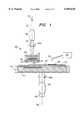
- FIG. 1illustrates an expanded schematic elevational view of an exemplary embodiment of a CMP apparatus constructed according to the principles of the present invention
- FIG. 2Aillustrates a simplified, enlarged sectional view of a conventional carrier head and conventional polishing platen during polishing
- FIG. 3illustrates an enlarged sectional view of the carrier head and polishing platen of FIG. 1.
- the CMP apparatuscomprises a polishing platen 110, a first rotatable shaft 120, a carrier head 130 having a carrier ring 133, a polishing pad 140, a first drive motor 150, a temperature controlled reservoir 160 for slurry delivery, a second rotatable shaft 137, and a second drive motor 180.
- the polishing pad 140provides a polishing surface 142 upon which a slurry 162 is deposited for polishing an object 170.
- the polishing platen 110is substantially horizontal and acts as a surface against which the object 170 may be planarized.
- the object 170is a semiconductor wafer.
- this particular embodimentis quite useful in the fabrication of integrated circuits formed on semiconductor wafers.
- embodiments described in FIG. 1includes magnetic regions in both the carrier head 130 and the polishing platen 110.
- embodimentsmay also be constructed with a single magnetic region in the carrier head 130 while constructing the opposing body, such as the polishing platen 110, of a magnetically responsive material, e.g., steel.
- embodimentscan be constructed with a single magnetic region in the polishing platen 110 while the carrier head 130 or retaining ring 133 is constructed of the magnetically responsive material.
- the rotatable shaft 137is coupled to the carrier head 130 and has an axis A 1 that is substantially normal to the polishing surface 142.
- the carrier head 130comprises a first magnetic region 131 and is rotatable by the rotatable shaft 137 about the axis A 1 .
- the first magnetic region 131may be a permanent magnetic region comprising a material such as lodestone.
- the first magnetic region 131may be a soft magnetic material, such as dead annealed iron.
- the magnetic regionmay be electromagnetic in nature, which allows for a variation in the strength of a magnetic force 135 by varying an electrical current through the electromagnetic region 131.
- the electromagnetic properties within the electromagnetic region 131may be induced by a magnetic coil that is formed in either the carrier head 130 or the polishing platen 110.
- the magnetic coilmay be connected to power source (not shown) through a rheostat that allows precise control of current flow through the magnetic coil.
- the first magnetic region 131is so configured that a surface 132 of the region 131 is a magnetic pole of a specific polarity, e.g., a north magnetic pole, as shown.
- the carrier head 130further comprises a retaining ring 133 that is configured to retain the semiconductor wafer 170 during polishing.
- the rotatable shaft 137 and carrier head 130are mounted to the second drive motor 180 for continuous rotation about axis A 1 in a direction indicated by arrow 137a.
- the polishing platen 110comprises a second magnetic region 111 and is rotatable by the rotatable shaft 120 about an axis A 2 .
- the second magnetic region 111may be a permanent magnetic region, a soft magnetic region, or an electromagnetic region.
- the second magnetic region 111is so configured that a surface 112 of the region 111 proximate the first magnetic region 131 is a magnetic pole of a specific polarity opposite the magnetic polarity of the surface 132 of the first magnetic region 131, i.e., a south magnetic pole, as shown.
- the exact polarity chosen for the first magnetic region 131 or second magnetic region 111is not important so long as the regions 111, 131 present opposite polarities to each other.
- the attractive force 135is created between the first and second magnetic regions 131, 111 and the carrier head 130 and polishing platen 110 to which the magnetic regions 131, 111 are attached, respectively.
- the first and second magnetic regions 131, 111may both be electromagnetic or permanent magnetic regions.
- currentmay be varied through the electromagnetic regions 111, 131 so that a desired magnitude of the attractive force 135 is exerted on the semiconductor wafer 170 and may be controlled as needed.
- One who is skilled in the artis familiar with changing the properties of an electromagnet by varying current therethrough.
- the semiconductor wafer 170by way of the carrier head 130 and the rotatable shaft 137, is engageable against the polishing pad 140.
- the carrier head 130further comprises the retaining ring 133 that prevents the semiconductor wafer 170 from fleeing the carrier head 130 under the forces of rotation.
- the illustrated embodiment employing two drive motorsis only one of several ways for implementing rotation of the carrier head 130 and polishing platen 110, and in no way limits the scope or intent of the present invention.
- the faces of the carrier head 130 and the semiconductor wafer 170have an operating angle substantially normal to the rotatable shaft 137; that is the operating angle is between about 85° and 90° as measured from the axis A 1 .
- the polishing platen 110is coupled to and rotated by the first rotatable shaft 120 driven by the first motor 150.
- the polishing platen 110 and first rotatable shaft 120are rotated about an axis A 2 that is substantially parallel to the axis A 1 .
- the second rotatable shaft 137 and the first rotatable shaft 120rotate in the same direction indicated by arrows 137a, 120a, respectively.
- the polishing slurry 162containing an abrasive such as silica or alumina particles suspended in either a basic or an acidic solution, is dispensed onto the polishing surface 142 through a conduit 163 from the temperature controlled reservoir 160.
- a conventional carrier head 230comprises a carrier body 231, a retaining ring 233, and a pneumatic interface 238.
- a conventional polishing surface 201comprises a polishing platen 210, and a polishing pad 240.
- the polishing pad 240will develop a ripple 242 at a free edge 271 of whatever surface 272 is being polished.
- One who is skilled in the artis familiar with the ripple 242 effect on the polishing pad 240 as the carrier head 230, semiconductor wafer 270, polishing platen 210, and polishing pad 240 rotate during polishing.
- the free edge 271 contactedis on the retaining ring 233 that is being forced against the polishing pad 240 by a force 239 generated by the pneumatic interface 238.
- the retaining ring 233prevents the ripple 242 from contacting an outer edge 273 of the semiconductor wafer 270 and rounding the outer edge 273.
- a pneumatic interface 238is used to force the retaining ring 233 against the pad 240 and move the ripple 242 radially outward.
- the pneumatic interface 238may be a relatively complicated system requiring pneumatic lines, seals and actuators (not shown) to assure the retaining ring 233 remains in contact with the polishing pad 240. Moreover, such pneumatic systems do not have the same degree of polishing control as the magnetic system provided by the present invention.
- the carrier head 130comprises the first magnetic region 131, the retaining ring 133, and a third magnetic region 338 within the retaining ring 133.
- the third magnetic region 338may be a permanent magnetic region or an electromagnetic region.
- the polishing platen 110comprises a second magnetic region 111 of an opposite magnetic polarity to the first magnetic region 131.
- the third magnetic region 338comprises an electromagnetic region, the strength of which can be controlled by an electric current. Therefore, a retaining ring attractive force 339 may be created between the third magnetic region 338 and the second magnetic region 111, thereby attracting the retaining ring 133 toward the polishing platen 110 and forcing a ripple 342 to an outer edge 332 of the retaining ring 133.
- creating the force 339 to control the vertical position of the retaining ring 133is simplified by the present invention that can adjust the force 339 by controlling currents in the first or third magnetic regions 111, 338.
- Providing rotary electrical contacts, a feature well known in the art, and electrical current to the third magnetic region 338is a significantly less difficult engineering problem than the prior art pneumatic system, discussed above in FIG. 2.
- the wafer 170is placed under the carrier head 130 and within the retaining ring 133.
- the carrier head 130 and polishing platen 110are rotated as indicated at 137a and 120a. Electric current is fed to the first and second electromagnetic regions 131, 111, creating opposite magnetic polarities in the first and second electromagnetic regions 131, 111 and therefore a downward force 135 of the carrier head 130 against the polishing platen 110.
- Electric currentmay also be fed to the third electromagnetic region 338 so as to create a similar downward retaining ring force 339 that keeps the retaining ring 133 in contact with the polishing pad 140, thereby forcing the ripple 342 to an outermost edge 371 of the retaining ring 133 and protecting the semiconductor wafer 170.
- a carrier head 130 and polishing platen 110 incorporating magnetic regions 131, 111, respectively,have been described that cooperate to provide an electrically adjustable polishing force 135 between the carrier head 130 and the polishing platen 110.
- This adjustable polishing force 135may be more precisely controlled than the load cells of prior art by controlling a current in the electromagnetic regions 131, 111 within the carrier head 130 and the polishing platen 110, respectively.
- a retaining ring 133 incorporating a third magnetic region 338has been described that cooperates with the second magnetic region 111 to create an adjustable force 339 between the retaining ring 133 and the polishing platen 110.
- This forcecauses the ripple 342 of the polishing pad 140 to move radially outward to the outer edge 371 of the retaining ring 133 thereby protecting the semiconductor wafer 170 from edge rounding.
- Using a magnetic forcesimplifies the design of the retaining ring 133 by eliminating the pneumatic system of the prior art.
Landscapes
- Engineering & Computer Science (AREA)
- Mechanical Engineering (AREA)
- Finish Polishing, Edge Sharpening, And Grinding By Specific Grinding Devices (AREA)
- Mechanical Treatment Of Semiconductor (AREA)
Abstract
Description
Claims (20)
Priority Applications (1)
| Application Number | Priority Date | Filing Date | Title |
|---|---|---|---|
| US09/237,082US6059638A (en) | 1999-01-25 | 1999-01-25 | Magnetic force carrier and ring for a polishing apparatus |
Applications Claiming Priority (1)
| Application Number | Priority Date | Filing Date | Title |
|---|---|---|---|
| US09/237,082US6059638A (en) | 1999-01-25 | 1999-01-25 | Magnetic force carrier and ring for a polishing apparatus |
Publications (1)
| Publication Number | Publication Date |
|---|---|
| US6059638Atrue US6059638A (en) | 2000-05-09 |
Family
ID=22892267
Family Applications (1)
| Application Number | Title | Priority Date | Filing Date |
|---|---|---|---|
| US09/237,082Expired - Fee RelatedUS6059638A (en) | 1999-01-25 | 1999-01-25 | Magnetic force carrier and ring for a polishing apparatus |
Country Status (1)
| Country | Link |
|---|---|
| US (1) | US6059638A (en) |
Cited By (36)
| Publication number | Priority date | Publication date | Assignee | Title |
|---|---|---|---|---|
| US6179694B1 (en)* | 1999-09-13 | 2001-01-30 | Chartered Semiconductor Manufacturing Ltd. | Extended guide rings with built-in slurry supply line |
| US6234868B1 (en)* | 1999-04-30 | 2001-05-22 | Lucent Technologies Inc. | Apparatus and method for conditioning a polishing pad |
| US6261958B1 (en)* | 1997-10-08 | 2001-07-17 | Lucent Technologies Inc. | Method for performing chemical-mechanical polishing |
| US6354928B1 (en)* | 2000-04-21 | 2002-03-12 | Agere Systems Guardian Corp. | Polishing apparatus with carrier ring and carrier head employing like polarities |
| US6368968B1 (en)* | 2000-04-11 | 2002-04-09 | Vanguard International Semiconductor Corporation | Ditch type floating ring for chemical mechanical polishing |
| US6436828B1 (en)* | 2000-05-04 | 2002-08-20 | Applied Materials, Inc. | Chemical mechanical polishing using magnetic force |
| US6482077B1 (en) | 1998-10-28 | 2002-11-19 | Micron Technology, Inc. | Method and apparatus for releasably attaching a polishing pad to a chemical-mechanical planarization machine |
| US20040038625A1 (en)* | 2002-08-23 | 2004-02-26 | Nagasubramaniyan Chandrasekaran | Carrier assemblies, planarizing apparatuses including carrier assemblies, and methods for planarizing micro-device workpieces |
| US20040094269A1 (en)* | 2001-07-25 | 2004-05-20 | Brown Nathan R. | Methods for determining amounts and locations of differential pressure to be applied to semiconductor substrates during polishing of semiconductor device structures carried thereby and for subsequently polishing similar semiconductor device structures |
| US20040142092A1 (en)* | 2003-01-18 | 2004-07-22 | Jason Long | Marshmallow |
| US20040142635A1 (en)* | 2003-01-16 | 2004-07-22 | Elledge Jason B. | Carrier assemblies, polishing machines including carrier assemblies, and methods for polishing micro-device workpieces |
| US20040214514A1 (en)* | 2003-04-28 | 2004-10-28 | Elledge Jason B. | Polishing machines including under-pads and methods for mechanical and/or chemical-mechanical polishing of microfeature workpieces |
| US6855032B1 (en)* | 2003-11-24 | 2005-02-15 | Nikon Corporation | Fine force control of actuators for chemical mechanical polishing apparatuses |
| US20050197045A1 (en)* | 2003-11-24 | 2005-09-08 | Novak W. T. | Fine force control of actuators for chemical mechanical polishing apparatuses |
| US20050282470A1 (en)* | 2004-06-16 | 2005-12-22 | Cabot Microelectronics Corporation | Continuous contour polishing of a multi-material surface |
| US20060035564A1 (en)* | 2003-11-24 | 2006-02-16 | Nikon Corporation | Fine force actuator assembly for chemical mechanical polishing apparatuses |
| US20060148386A1 (en)* | 2003-07-15 | 2006-07-06 | Hoya Corporation | Method and device for manufacturing substrate for magnetic disk, and method of manufacturing magnetic disk |
| US20060160474A1 (en)* | 2005-01-15 | 2006-07-20 | Ming-Kuei Tseng | Magnetically secured retaining ring |
| US20060189256A1 (en)* | 2005-02-22 | 2006-08-24 | Lsi Logic Corporation | Systems and methods for wafer polishing |
| US20060189257A1 (en)* | 2005-02-22 | 2006-08-24 | Lsi Logic Corporation | Systems and methods for wafer polishing |
| US7108591B1 (en)* | 2004-03-31 | 2006-09-19 | Lam Research Corporation | Compliant wafer chuck |
| US20060286906A1 (en)* | 2005-06-21 | 2006-12-21 | Cabot Microelectronics Corporation | Polishing pad comprising magnetically sensitive particles and method for the use thereof |
| US20070232193A1 (en)* | 2006-03-31 | 2007-10-04 | Hozumi Yasuda | Substrate holding apparatus, polishing apparatus, and polishing method |
| US20080051008A1 (en)* | 2006-08-22 | 2008-02-28 | International Business Machines Corporation | Apparatus and method for chemical mechanical polishing with improved uniformity |
| US20080271384A1 (en)* | 2006-09-22 | 2008-11-06 | Saint-Gobain Ceramics & Plastics, Inc. | Conditioning tools and techniques for chemical mechanical planarization |
| WO2013166375A1 (en)* | 2012-05-04 | 2013-11-07 | Saint-Gobain Abrasives, Inc. | Tool for use with dual-sided chemical mechanical planarization pad conditioner |
| US8905823B2 (en) | 2009-06-02 | 2014-12-09 | Saint-Gobain Abrasives, Inc. | Corrosion-resistant CMP conditioning tools and methods for making and using same |
| US8951099B2 (en) | 2009-09-01 | 2015-02-10 | Saint-Gobain Abrasives, Inc. | Chemical mechanical polishing conditioner |
| US20150111477A1 (en)* | 2013-10-18 | 2015-04-23 | Taiwan Semiconductor Manufacturing Co., Ltd. | Polishing Head, Chemical-Mechanical Polishing System, and Method for Polishing Substrate |
| US9022840B2 (en) | 2009-03-24 | 2015-05-05 | Saint-Gobain Abrasives, Inc. | Abrasive tool for use as a chemical mechanical planarization pad conditioner |
| CN106345711A (en)* | 2016-11-17 | 2017-01-25 | 嘉兴市日新自动化科技有限公司 | Magnet powder removal machine |
| US20180361525A1 (en)* | 2017-06-16 | 2018-12-20 | Taiwan Semiconductor Manufacturing Company Ltd. | Chemical mechanical polishing apparatus, slurry, and method of using the same |
| US10593554B2 (en) | 2015-04-14 | 2020-03-17 | Jun Yang | Method and apparatus for within-wafer profile localized tuning |
| US20220009053A1 (en)* | 2020-07-08 | 2022-01-13 | Applied Materials, Inc. | Multi-toothed, magnetically controlled retaining ring |
| US11590628B2 (en) | 2019-07-08 | 2023-02-28 | Samsung Electronics Co., Ltd. | Rotary body module and chemical mechanical polishing apparatus having the same |
| US20240217054A1 (en)* | 2019-09-17 | 2024-07-04 | Taiwan Semiconductor Manufacturing Co., Ltd. | Chemical mechanical polishing apparatus and method |
Citations (2)
| Publication number | Priority date | Publication date | Assignee | Title |
|---|---|---|---|---|
| US3801293A (en)* | 1972-06-05 | 1974-04-02 | Timesavers Inc | Method of machining ferromagnetic workpieces to true flatness |
| US4222204A (en)* | 1979-06-18 | 1980-09-16 | Benner Robert L | Holder for an abrasive plate |
- 1999
- 1999-01-25USUS09/237,082patent/US6059638A/ennot_activeExpired - Fee Related
Patent Citations (2)
| Publication number | Priority date | Publication date | Assignee | Title |
|---|---|---|---|---|
| US3801293A (en)* | 1972-06-05 | 1974-04-02 | Timesavers Inc | Method of machining ferromagnetic workpieces to true flatness |
| US4222204A (en)* | 1979-06-18 | 1980-09-16 | Benner Robert L | Holder for an abrasive plate |
Cited By (82)
| Publication number | Priority date | Publication date | Assignee | Title |
|---|---|---|---|---|
| US6261958B1 (en)* | 1997-10-08 | 2001-07-17 | Lucent Technologies Inc. | Method for performing chemical-mechanical polishing |
| US6602380B1 (en) | 1998-10-28 | 2003-08-05 | Micron Technology, Inc. | Method and apparatus for releasably attaching a polishing pad to a chemical-mechanical planarization machine |
| US7001251B2 (en)* | 1998-10-28 | 2006-02-21 | Micron Technology, Inc. | Method and apparatus for releasably attaching a polishing pad to a chemical-mechanical planarization machine |
| US6663470B2 (en) | 1998-10-28 | 2003-12-16 | Micron Technology, Inc. | Method and apparatus for releasably attaching a polishing pad to a chemical-mechanical planarization machine |
| US6482077B1 (en) | 1998-10-28 | 2002-11-19 | Micron Technology, Inc. | Method and apparatus for releasably attaching a polishing pad to a chemical-mechanical planarization machine |
| US6506101B2 (en) | 1998-10-28 | 2003-01-14 | Micron Technology, Inc. | Method and apparatus for releasably attaching a polishing pad to a chemical-mechanical planarization machine |
| US6514125B2 (en) | 1998-10-28 | 2003-02-04 | Micron Technology, Inc. | Method and apparatus for releasably attaching a polishing pad to a chemical-mechanical planarization machine |
| US6585575B2 (en) | 1998-10-28 | 2003-07-01 | Micron Technology, Inc. | Method and apparatus for releasably attaching a polishing pad to a chemical-mechanical planarization machine |
| US6234868B1 (en)* | 1999-04-30 | 2001-05-22 | Lucent Technologies Inc. | Apparatus and method for conditioning a polishing pad |
| US6179694B1 (en)* | 1999-09-13 | 2001-01-30 | Chartered Semiconductor Manufacturing Ltd. | Extended guide rings with built-in slurry supply line |
| US6776870B2 (en)* | 2000-04-11 | 2004-08-17 | Vanguard International Semiconductor Corp. | Ditch type floating ring for chemical mechanical polishing |
| US6368968B1 (en)* | 2000-04-11 | 2002-04-09 | Vanguard International Semiconductor Corporation | Ditch type floating ring for chemical mechanical polishing |
| US6354928B1 (en)* | 2000-04-21 | 2002-03-12 | Agere Systems Guardian Corp. | Polishing apparatus with carrier ring and carrier head employing like polarities |
| US6436828B1 (en)* | 2000-05-04 | 2002-08-20 | Applied Materials, Inc. | Chemical mechanical polishing using magnetic force |
| US7285037B2 (en) | 2001-07-25 | 2007-10-23 | Micron Technology, Inc. | Systems including differential pressure application apparatus |
| US7935216B2 (en) | 2001-07-25 | 2011-05-03 | Round Rock Research, Llc | Differential pressure application apparatus for use in polishing layers of semiconductor device structures and methods |
| US7059937B2 (en) | 2001-07-25 | 2006-06-13 | Micron Technology, Inc. | Systems including differential pressure application apparatus |
| US20040094269A1 (en)* | 2001-07-25 | 2004-05-20 | Brown Nathan R. | Methods for determining amounts and locations of differential pressure to be applied to semiconductor substrates during polishing of semiconductor device structures carried thereby and for subsequently polishing similar semiconductor device structures |
| US20050229369A1 (en)* | 2001-07-25 | 2005-10-20 | Brown Nathan R | Systems including differential pressure application apparatus |
| US20040102144A1 (en)* | 2001-07-25 | 2004-05-27 | Brown Nathan R. | Polishing systems for use with semiconductor substrates including differential pressure application apparatus |
| US20040108064A1 (en)* | 2001-07-25 | 2004-06-10 | Brown Nathan R. | Methods for polishing semiconductor device structures by differentially applying pressure to substrates that carry the semiconductor device structures |
| US8268115B2 (en) | 2001-07-25 | 2012-09-18 | Round Rock Research, Llc | Differential pressure application apparatus for use in polishing layers of semiconductor device structures and methods |
| US6863771B2 (en) | 2001-07-25 | 2005-03-08 | Micron Technology, Inc. | Differential pressure application apparatus for use in polishing layers of semiconductor device structures and methods |
| US6899607B2 (en) | 2001-07-25 | 2005-05-31 | Micron Technology, Inc. | Polishing systems for use with semiconductor substrates including differential pressure application apparatus |
| US7947190B2 (en) | 2001-07-25 | 2011-05-24 | Round Rock Research, Llc | Methods for polishing semiconductor device structures by differentially applying pressure to substrates that carry the semiconductor device structures |
| US20050142807A1 (en)* | 2001-07-25 | 2005-06-30 | Brown Nathan R. | Differential pressure application apparatus for use in polishing layers of semiconductor device structures and method |
| US7004817B2 (en)* | 2002-08-23 | 2006-02-28 | Micron Technology, Inc. | Carrier assemblies, planarizing apparatuses including carrier assemblies, and methods for planarizing micro-device workpieces |
| US6958001B2 (en)* | 2002-08-23 | 2005-10-25 | Micron Technology, Inc. | Carrier assemblies, planarizing apparatuses including carrier assemblies, and methods for planarizing micro-device workpieces |
| US20050260927A1 (en)* | 2002-08-23 | 2005-11-24 | Micron Technology, Inc. | Carrier assemblies, planarizing apparatuses including carrier assemblies, and methods for planarizing micro-device workpieces |
| US20040038625A1 (en)* | 2002-08-23 | 2004-02-26 | Nagasubramaniyan Chandrasekaran | Carrier assemblies, planarizing apparatuses including carrier assemblies, and methods for planarizing micro-device workpieces |
| US20050118930A1 (en)* | 2002-08-23 | 2005-06-02 | Nagasubramaniyan Chandrasekaran | Carrier assemblies, planarizing apparatuses including carrier assemblies, and methods for planarizing micro-device workpieces |
| US7147543B2 (en)* | 2002-08-23 | 2006-12-12 | Micron Technology, Inc. | Carrier assemblies, planarizing apparatuses including carrier assemblies, and methods for planarizing micro-device workpieces |
| US20050026544A1 (en)* | 2003-01-16 | 2005-02-03 | Elledge Jason B. | Carrier assemblies, polishing machines including carrier assemblies, and methods for polishing micro-device workpieces |
| US7074114B2 (en)* | 2003-01-16 | 2006-07-11 | Micron Technology, Inc. | Carrier assemblies, polishing machines including carrier assemblies, and methods for polishing micro-device workpieces |
| US20050255792A1 (en)* | 2003-01-16 | 2005-11-17 | Micron Technology, Inc. | Carrier assemblies, polishing machines including carrier assemblies, and methods for polishing micro-device workpieces |
| US20040142635A1 (en)* | 2003-01-16 | 2004-07-22 | Elledge Jason B. | Carrier assemblies, polishing machines including carrier assemblies, and methods for polishing micro-device workpieces |
| US7255630B2 (en)* | 2003-01-16 | 2007-08-14 | Micron Technology, Inc. | Methods of manufacturing carrier heads for polishing micro-device workpieces |
| US7033251B2 (en)* | 2003-01-16 | 2006-04-25 | Micron Technology, Inc. | Carrier assemblies, polishing machines including carrier assemblies, and methods for polishing micro-device workpieces |
| US20040142092A1 (en)* | 2003-01-18 | 2004-07-22 | Jason Long | Marshmallow |
| US20040214514A1 (en)* | 2003-04-28 | 2004-10-28 | Elledge Jason B. | Polishing machines including under-pads and methods for mechanical and/or chemical-mechanical polishing of microfeature workpieces |
| US6935929B2 (en) | 2003-04-28 | 2005-08-30 | Micron Technology, Inc. | Polishing machines including under-pads and methods for mechanical and/or chemical-mechanical polishing of microfeature workpieces |
| US20060148386A1 (en)* | 2003-07-15 | 2006-07-06 | Hoya Corporation | Method and device for manufacturing substrate for magnetic disk, and method of manufacturing magnetic disk |
| US7175511B2 (en)* | 2003-07-15 | 2007-02-13 | Hoya Corporation | Method of manufacturing substrate for magnetic disk, apparatus for manufacturing substrate for magnetic disk, and method of manufacturing magnetic disk |
| US6855032B1 (en)* | 2003-11-24 | 2005-02-15 | Nikon Corporation | Fine force control of actuators for chemical mechanical polishing apparatuses |
| US20050197045A1 (en)* | 2003-11-24 | 2005-09-08 | Novak W. T. | Fine force control of actuators for chemical mechanical polishing apparatuses |
| US7172493B2 (en) | 2003-11-24 | 2007-02-06 | Nikon Corporation | Fine force actuator assembly for chemical mechanical polishing apparatuses |
| US20060035564A1 (en)* | 2003-11-24 | 2006-02-16 | Nikon Corporation | Fine force actuator assembly for chemical mechanical polishing apparatuses |
| US7108591B1 (en)* | 2004-03-31 | 2006-09-19 | Lam Research Corporation | Compliant wafer chuck |
| US20050282470A1 (en)* | 2004-06-16 | 2005-12-22 | Cabot Microelectronics Corporation | Continuous contour polishing of a multi-material surface |
| US7198549B2 (en) | 2004-06-16 | 2007-04-03 | Cabot Microelectronics Corporation | Continuous contour polishing of a multi-material surface |
| US7134948B2 (en) | 2005-01-15 | 2006-11-14 | Applied Materials, Inc. | Magnetically secured retaining ring |
| US20060160474A1 (en)* | 2005-01-15 | 2006-07-20 | Ming-Kuei Tseng | Magnetically secured retaining ring |
| US7201633B2 (en)* | 2005-02-22 | 2007-04-10 | Lsi Logic Corporation | Systems and methods for wafer polishing |
| US20060189256A1 (en)* | 2005-02-22 | 2006-08-24 | Lsi Logic Corporation | Systems and methods for wafer polishing |
| US20060189257A1 (en)* | 2005-02-22 | 2006-08-24 | Lsi Logic Corporation | Systems and methods for wafer polishing |
| US20060286906A1 (en)* | 2005-06-21 | 2006-12-21 | Cabot Microelectronics Corporation | Polishing pad comprising magnetically sensitive particles and method for the use thereof |
| US7967665B2 (en)* | 2006-03-31 | 2011-06-28 | Ebara Corporation | Substrate holding apparatus, polishing apparatus, and polishing method |
| US20080318492A1 (en)* | 2006-03-31 | 2008-12-25 | Hozumi Yasuda | Substrate holding apparatus, polishing apparatus, and polishing method |
| US20080318499A1 (en)* | 2006-03-31 | 2008-12-25 | Hozumi Yasuda | Substrate holding apparatus, polishing apparatus, and polishing method |
| US8100739B2 (en) | 2006-03-31 | 2012-01-24 | Ebara Corporation | Substrate holding apparatus, polishing apparatus, and polishing method |
| US8267746B2 (en)* | 2006-03-31 | 2012-09-18 | Ebara Corporation | Substrate holding apparatus, polishing apparatus, and polishing method |
| EP1839812A3 (en)* | 2006-03-31 | 2008-01-02 | Ebara Corporation | Substrate holding apparatus, polishing apparatus, and polishing method |
| US8485866B2 (en) | 2006-03-31 | 2013-07-16 | Ebara Corporation | Substrate holding apparatus, polishing apparatus, and polishing method |
| US20070232193A1 (en)* | 2006-03-31 | 2007-10-04 | Hozumi Yasuda | Substrate holding apparatus, polishing apparatus, and polishing method |
| US20080051008A1 (en)* | 2006-08-22 | 2008-02-28 | International Business Machines Corporation | Apparatus and method for chemical mechanical polishing with improved uniformity |
| US20080271384A1 (en)* | 2006-09-22 | 2008-11-06 | Saint-Gobain Ceramics & Plastics, Inc. | Conditioning tools and techniques for chemical mechanical planarization |
| US9022840B2 (en) | 2009-03-24 | 2015-05-05 | Saint-Gobain Abrasives, Inc. | Abrasive tool for use as a chemical mechanical planarization pad conditioner |
| US8905823B2 (en) | 2009-06-02 | 2014-12-09 | Saint-Gobain Abrasives, Inc. | Corrosion-resistant CMP conditioning tools and methods for making and using same |
| US8951099B2 (en) | 2009-09-01 | 2015-02-10 | Saint-Gobain Abrasives, Inc. | Chemical mechanical polishing conditioner |
| US20130316630A1 (en)* | 2012-05-04 | 2013-11-28 | Michael Rothenberg | Tool for use with dual-sided chemical mechanical planarization pad conditioner |
| WO2013166375A1 (en)* | 2012-05-04 | 2013-11-07 | Saint-Gobain Abrasives, Inc. | Tool for use with dual-sided chemical mechanical planarization pad conditioner |
| US20150111477A1 (en)* | 2013-10-18 | 2015-04-23 | Taiwan Semiconductor Manufacturing Co., Ltd. | Polishing Head, Chemical-Mechanical Polishing System, and Method for Polishing Substrate |
| US9272386B2 (en)* | 2013-10-18 | 2016-03-01 | Taiwan Semiconductor Manufacturing Co., Ltd. | Polishing head, and chemical-mechanical polishing system for polishing substrate |
| US9987720B2 (en) | 2013-10-18 | 2018-06-05 | Taiwan Semiconductor Manufacturing Co., Ltd. | Method for operating a polishing head and method for polishing a substrate |
| US10593554B2 (en) | 2015-04-14 | 2020-03-17 | Jun Yang | Method and apparatus for within-wafer profile localized tuning |
| CN106345711A (en)* | 2016-11-17 | 2017-01-25 | 嘉兴市日新自动化科技有限公司 | Magnet powder removal machine |
| US20180361525A1 (en)* | 2017-06-16 | 2018-12-20 | Taiwan Semiconductor Manufacturing Company Ltd. | Chemical mechanical polishing apparatus, slurry, and method of using the same |
| US11351648B2 (en)* | 2017-06-16 | 2022-06-07 | Taiwan Semiconductor Manufacturing Company Ltd. | Chemical mechanical polishing apparatus, slurry, and method of using the same |
| US11590628B2 (en) | 2019-07-08 | 2023-02-28 | Samsung Electronics Co., Ltd. | Rotary body module and chemical mechanical polishing apparatus having the same |
| US20240217054A1 (en)* | 2019-09-17 | 2024-07-04 | Taiwan Semiconductor Manufacturing Co., Ltd. | Chemical mechanical polishing apparatus and method |
| US20220009053A1 (en)* | 2020-07-08 | 2022-01-13 | Applied Materials, Inc. | Multi-toothed, magnetically controlled retaining ring |
| US11691244B2 (en)* | 2020-07-08 | 2023-07-04 | Applied Materials, Inc. | Multi-toothed, magnetically controlled retaining ring |
Similar Documents
| Publication | Publication Date | Title |
|---|---|---|
| US6059638A (en) | Magnetic force carrier and ring for a polishing apparatus | |
| US6354928B1 (en) | Polishing apparatus with carrier ring and carrier head employing like polarities | |
| US6863771B2 (en) | Differential pressure application apparatus for use in polishing layers of semiconductor device structures and methods | |
| US6309282B1 (en) | Variable abrasive polishing pad for mechanical and chemical-mechanical planarization | |
| US7033251B2 (en) | Carrier assemblies, polishing machines including carrier assemblies, and methods for polishing micro-device workpieces | |
| US5177908A (en) | Polishing pad | |
| US5593537A (en) | Apparatus for processing semiconductor wafers | |
| US6213855B1 (en) | Self-powered carrier for polishing or planarizing wafers | |
| TW201609313A (en) | Method, system and polishing pad for chemical mechancal polishing | |
| JP2006524587A (en) | Polishing machine and method including an underpad for mechanically and / or chemically mechanically polishing a micro-shaped workpiece | |
| TW491748B (en) | Subaperture chemical mechanical polishing system | |
| US20040038625A1 (en) | Carrier assemblies, planarizing apparatuses including carrier assemblies, and methods for planarizing micro-device workpieces | |
| CN112518572A (en) | Chemical mechanical polishing method | |
| KR100222186B1 (en) | Manufacturing Method of Semiconductor Device and Semiconductor Manufacturing Device | |
| US6180423B1 (en) | Method for wafer polishing and method for polishing pad dressing | |
| KR100562498B1 (en) | Pad conditioner of CMP equipment | |
| US6121142A (en) | Magnetic frictionless gimbal for a polishing apparatus | |
| US7025854B2 (en) | Method and apparatus for aligning and setting the axis of rotation of spindles of a multi-body system | |
| JP2003053657A (en) | Polishing surface structural member and polishing device using the same | |
| JPH09225820A (en) | Polishing equipment | |
| JPH08155831A (en) | Polishing device and polishing method | |
| US6054017A (en) | Chemical mechanical polishing pad with controlled polish rate | |
| JP2022162416A (en) | Surface treatment device | |
| WO2015050642A1 (en) | Cmp equipment using magnet responsive composites | |
| US20020058466A1 (en) | Method and system for reducing thickness of spin-on glass on semiconductor wafers |
Legal Events
| Date | Code | Title | Description |
|---|---|---|---|
| AS | Assignment | Owner name:LUCENT TECHNOLOGIES INC., NEW JERSEY Free format text:ASSIGNMENT OF ASSIGNORS INTEREST;ASSIGNORS:CREVASSE, ANNETTE M.;EASTER, WILLIAM G.;MAZE, JOHN A.;AND OTHERS;REEL/FRAME:009733/0211 Effective date:19990122 | |
| AS | Assignment | Owner name:THE CHASE MANHATTAN BANK, AS COLLATERAL AGENT, TEX Free format text:CONDITIONAL ASSIGNMENT OF AND SECURITY INTEREST IN PATENT RIGHTS;ASSIGNOR:LUCENT TECHNOLOGIES INC. (DE CORPORATION);REEL/FRAME:011722/0048 Effective date:20010222 | |
| REMI | Maintenance fee reminder mailed | ||
| LAPS | Lapse for failure to pay maintenance fees | ||
| FP | Lapsed due to failure to pay maintenance fee | Effective date:20040509 | |
| AS | Assignment | Owner name:LUCENT TECHNOLOGIES INC., NEW JERSEY Free format text:TERMINATION AND RELEASE OF SECURITY INTEREST IN PATENT RIGHTS;ASSIGNOR:JPMORGAN CHASE BANK, N.A. (FORMERLY KNOWN AS THE CHASE MANHATTAN BANK), AS ADMINISTRATIVE AGENT;REEL/FRAME:018590/0047 Effective date:20061130 | |
| STCH | Information on status: patent discontinuation | Free format text:PATENT EXPIRED DUE TO NONPAYMENT OF MAINTENANCE FEES UNDER 37 CFR 1.362 |