US6057802A - Trimmed foursquare antenna radiating element - Google Patents
Trimmed foursquare antenna radiating elementDownload PDFInfo
- Publication number
- US6057802A US6057802AUS09/326,688US32668899AUS6057802AUS 6057802 AUS6057802 AUS 6057802AUS 32668899 AUS32668899 AUS 32668899AUS 6057802 AUS6057802 AUS 6057802A
- Authority
- US
- United States
- Prior art keywords
- radiating elements
- foursquare
- pairs
- dielectric layer
- array
- Prior art date
- Legal status (The legal status is an assumption and is not a legal conclusion. Google has not performed a legal analysis and makes no representation as to the accuracy of the status listed.)
- Expired - Fee Related
Links
Images


Classifications
- H—ELECTRICITY
- H01—ELECTRIC ELEMENTS
- H01Q—ANTENNAS, i.e. RADIO AERIALS
- H01Q9/00—Electrically-short antennas having dimensions not more than twice the operating wavelength and consisting of conductive active radiating elements
- H01Q9/04—Resonant antennas
- H01Q9/0407—Substantially flat resonant element parallel to ground plane, e.g. patch antenna
- H—ELECTRICITY
- H01—ELECTRIC ELEMENTS
- H01Q—ANTENNAS, i.e. RADIO AERIALS
- H01Q21/00—Antenna arrays or systems
- H01Q21/24—Combinations of antenna units polarised in different directions for transmitting or receiving circularly and elliptically polarised waves or waves linearly polarised in any direction
- H01Q21/245—Combinations of antenna units polarised in different directions for transmitting or receiving circularly and elliptically polarised waves or waves linearly polarised in any direction provided with means for varying the polarisation
- H—ELECTRICITY
- H01—ELECTRIC ELEMENTS
- H01Q—ANTENNAS, i.e. RADIO AERIALS
- H01Q9/00—Electrically-short antennas having dimensions not more than twice the operating wavelength and consisting of conductive active radiating elements
- H01Q9/04—Resonant antennas
- H01Q9/0407—Substantially flat resonant element parallel to ground plane, e.g. patch antenna
- H01Q9/045—Substantially flat resonant element parallel to ground plane, e.g. patch antenna with particular feeding means
Definitions
- the present inventiongenerally relates to an antenna radiating element and, more particularly, to a foursquare antenna element which can provide dual polarization useful in, for example, compact, wideband radar and communication antenna arrays.
- An antennais a transducer between free space propagation and guided wave propagation of electromagnetic waves. During a transmission, the antenna concentrates radiated energy into a shaped directive beam which illuminates targets in a desired direction.
- the targetis some physical object, the presence of which is to be determined.
- the targetmay be a receiving antenna.
- the antennacollects energy from the free space propagation. In a radar system, this energy comprises a signal reflected back to the antenna from a target. Hence, in a radar system, a single antenna may be used to both transmit and receive signals. Likewise in a communication system an antenna may serve the dual functions of transmitting and receiving signals from a remote antenna. In a radar system, the primary purpose of the antenna is to determine the angular direction of the target. A highly directive, narrow beam-width is needed in order to accurately determine angular direction as well as to resolve multiple targets in physically close proximity to one another.
- Phased array antenna systemsare formed from an arrayed combination of multiple, individual, similar radiator elements.
- the phased array antenna characteristicsare determined by the geometry and the relative positioning of the individual elements and the phase and amplitude of their excitation.
- the phased array antenna apertureis assembled from the individual radiating elements, such as, for example, dipoles or slots. By individually controlling the phase and amplitude of the elements very predictable radiation patterns and beam directions can be realized.
- the antenna aperturerefers to the physical area projected on a plane perpendicular to the main beam direction. Briefly, there are several important parameters which govern antenna performance. These include the radiation pattern (including polarization), gain, and the antenna impedance.
- the radiation patternrefers to the electromagnetic energy distribution in three-dimensional angular space. When normalized and plotted, it is referred to as the antenna radiation pattern.
- the direction of polarization of an antennais defined as the direction of the electric field (E-field) vector.
- E-fieldelectric field
- a radar antennais linearly polarized, in either the horizontal or the vertical direction using earth as a reference.
- circular and elliptical polarizationsare also common.
- the E-fieldvaries with time at any fixed observation point, tracing a circular locus once per RF (radio frequency) cycle in a fixed plane normal to the direction of propagation.
- Circular polarizationis useful, for example, to detect aircraft targets in the rain.
- elliptical polarizationtraces an elliptical locus once per RF cycle.
- Gaincomprises directive gain (referred to as "directivity” G D ) and power gain (referred to as simply “gain” G) and relates to the ability of the antenna to concentrate energy in a narrow angular regions.
- Directive gainor directivity, is defined as the maximum beam radiation intensity relative to the average intensity, usually given in units of watts per steradian.
- Directional gainmay also be expressed as maximum radiated power density (i.e., watts/meter 2 ) at a far field distance R relative to the average density at the same distance.
- Power gain, or simply gainis defined as power accepted at by the antenna input port, rather than radiated power.
- Antenna input impedanceis made up of the resistive and reactive components presented at the antenna feed.
- the resistive componentis the result of antenna radiation and ohmic losses.
- the reactive componentis the result of stored energy in the antenna.
- the resistive componentIn broad band antennas it is desirable for the resistive component to be constant with frequency and have a moderate value (50 Ohms, for example).
- the magnitude of the reactive componentshould be small (ideally zero). For most antennas the reactive component is small over a limited frequency range.
- Phased array antennas capable of scanninghave been know for some time. However, phased array antennas have had a resurgence for modem applications with the introduction of electronically controlled phase shifters and switches. Electronic control allows aperture excitement to be modulated by controlling the phase of the individual elements to realize beams that are scanned electronically.
- General information on phased array antennas and scanning principlescan be gleaned from Merrill Skolnik, Radar Handbook, second edition, McGraw-Hill, 1990, herein incorporated by reference. Phased array antennas lend themselves particularly well to radar and directional communication applications.
- the radiating elementshould be chosen to suit the feed system and the physical requirements of the antenna.
- the most commonly used radiators for phased arraysare dipoles, slots, open-ended waveguides (or small horns), and printed-circuit "patches".
- the elementhas to be small enough to fit in the array geometry, thereby limiting the element to an area of a little more than ⁇ /4, where ⁇ is wavelength.
- the antennaoperates by aggregating the contribution of each small radiator element at a distance, many radiators are required for the antenna to be effective.
- the radiating elementshould be inexpensive and reliable and have identical, predictable characteristics from unit to unit.
- Radiator elementssuch as the "four arm sinuous log-periodic", described in U.S. Pat. No. 4,658,262 to DuHamel, and the Archaemedian spiral, which have wide bandwidths and are otherwise desirable for array applications have diameters greater than 0.43 ⁇ at their lowest frequency. With a bandwidth in excess of 1.5:1 in a square grid array an interelement spacing of about 0.33 ⁇ is desired.
- a foursquare dual polarized moderately wide bandwidth antenna radiating elementwhich, due to its small size and low frequency response, is well suited to array applications.
- the foursquare elementcomprises a printed metalization on a low-loss substrate suspended over a ground plane reflector. Dual linear (i.e., horizontal and vertical), as well as circular and elliptical polarizations of any orientation may be produced with the inventive foursquare element.
- an array of such elementscan be modulated to produce a highly directive beam which can be scanned by adjusting the relative phase of the elements. Operation of the array is enhanced because the individual foursquare elements are small as compared to conventional array element having comparable frequency response. The small size allows for closer spacing of the individual elements which facilitates scanning.
- Bandwidths of 1.5:1 or bettermay be obtained with a feed point impedance of 50 Ohms. Good performance is obtained with the foursquare element having a size between 0.30 ⁇ and 0.40 ⁇ and preferably of 0.36 ⁇ . Also the foursquare element impedance degrades gradually in contrast to some elements such as the "four arm sinuous log-periodic" which has large impedance variations near its lowest frequency.
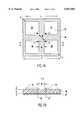
- FIGS. 1A and 1Bis a top view, and a cross-sectional view of the foursquare element according to the present invention, respectively;
- FIG. 2is a perspective view foursquare antenna element
- FIG. 3is a top view of the foursquare antenna element showing the feed points for various polarizations
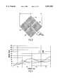
- FIG. 4is a feed point impedance plot for the foursquare antenna element
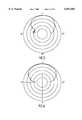
- FIG. 5is a mid-band E plane radiation pattern for the foursquare element
- FIG. 6is a mid-band H plane radiation pattern for the foursquare element
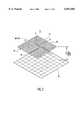
- FIG. 7is an illustrative geometry of a fully array comprised of many foursquare elements
- FIG. 8is a top view of a second embodiment of the present invention comprising a trimmed four-square antenna element configuration
- FIG. 9is a cross-sectional view of the trimmed four-square antenna element
- FIG. 10is a top view showing the geometry of the trimmed four-square antenna element
- FIG. 11is an E-plane co-polarized pattern of the trimmed foursquare for midband
- FIG. 12is an H-plane co-polarized pattern of the trimmed foursquare for midband
- FIG. 13is a graph showing the trimmed four-square input impedance
- FIGS. 14-35show various alternative embodiments comprising different ways of trimming the basic foursquare antenna as described above.
- the foursquare element 10comprises a four small square metalization regions 12, 14, 16, and 18 (petals) printed on a low loss substrate 20.
- the low loss substrate 20may be secured to a ground plane.
- Each of the small square regions 12, 14, 16, and 18,are separated by a narrow gap W on two sides and by a gap W' in the diagonal.
- Each elementis fed by balanced feed lines a--a' and b--b' attached at or near the center of the element diagonally across the gap W'.
- the element halvesi.e., 12 and 18, or 14 and 16
- the element halvescan be fed independently with either the same or different frequencies.
- either two independent transmission lines or a balanced four wire transmission lineis needed.
- the foursquare element 10can therefore be used to produce dual linear (i.e., vertical or horizontal polarization) or circular polarization of either sense similar to crossed dipoles.
- Appropriate feeding of the crossed element in the foursquare antennacan be used to produce various angles of linear or elliptical polarization.
- linear polarizationmay be obtained by feeding either element half (e.g., 12 and 18, or 14 and 16) diagonally across the gap W'. In this case the polarization will be in line with the diagonal of the feed.
- Other linear polarizationsmay be obtained by feeding both element halves in phase with one another. The angle of the polarization is determined by the relative amplitude of the sources. Circular polarization is obtained by feeding the crossed element halves in phase quadrature (i.e. 90 degree relationship) and equal amplitude.
- the foursquare element 10 of the present inventioncan be arranged into an array to produce a highly directive beam.
- the array beamcan then be scanned by adjusting the relative phase of the elements according to conventional practice.
- the foursquare element 10has the advantage of allowing relatively close spacing of adjacent elements, by arranging the elements so that the element sides are parallel to one another. When the elements are placed in this manner the principal polarization planes are diagonal to the sides of the array. If other polarization orientations are desired the array can be rotated. By applying excitation to the crossed element pairs (12 and 18, or 14 and 16) with equal and in-phase currents, a composite polarization oriented along the side of the elements and the array is produced. Other polarizations are produced in a similar manner.
- Ground plane spacings H of 1/4 wavelength ( ⁇ /4) or lessare appropriate and should be chosen with regard to the required feed point (a, a', b, and b') impedance characteristics, scanning characteristics and the dielectric characteristics of the substrate 20.
- a reasonable choicewould be a spacing H of ⁇ /4 at the highest frequency used when the substrate 20 is air. If the substrate 20 is composed of a dielectric material other than air the spacing H is approximately ⁇ /4 (again at the highest frequency) divided by the square root of the relative permittivity ⁇ R of the substrate 20.
- the frequency range of the foursquare element 10is limited to less than a 2:1 range by the low input resistance, increasing capacitive reactance at the lowest operating frequency, and by the rapid rise in impedance or anti-resonance which occurs at the high frequency end.
- Some narrow band applicationsmay be able to extend the low frequency response by use of conventional matching techniques.
- the lowest frequency of operation for the elementoccurs when the diagonal of the square element is approximately 1/2 wavelength ( ⁇ /2).
- the anti-resonance which limits the high frequency responseoccurs when the diagonal D across the element 10 becomes approximately one wavelength (D ⁇ ).
- D ⁇the diagonal D across the element 10.
- the anti-resonancemay not be approached closely however because of the rapidly increasing reactance.
- An early test element placed over a ground planegave a bandwidth of about 1.5:1 with the limits taken at a voltage standing wave ratio (vswr) of 2. This bandwidth would be typical of an uncompensated foursquare element.
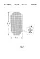
- FIG. 2shows a perspective view of the foursquare element according to the present invention superimposed on a Cartesian origin.
- the perspective viewis shown in wire grid representation for illustrative purposes; however, typically the elements would be solid printed metalizations.
- the ground plane 22lies parallel to the x-y plane and parallel to the plane of the elements 12, 14, 16, and 18.
- the elementsare typically printed in a dielectric substrate (not shown) having a approximate thickness of ⁇ /4.
- the feedis diagonal across the origin.
- the direction of maximum radiationis in the z direction.
- FIG. 3shows a top view of the foursquare element according to the present invention.
- the size of the diagonal D across the element 10is approximately ⁇ /2 at the lowest frequency.
- a transmission feed lineis connected across feed a--a'.
- connecting across b--b'gives a vertical polarization.
- the substrate 20was a layered composite material consisting of an upper layer of glass microfiber reinforced polytetrafluoroethylene, such as RT/duroid® 5870 having a thickness of 0.028 inches with 1 oz. copper cladding and a lower layer of polystyrene foam having a thickness of 0.250 inches.
- the four metalized regions 12, 14, 16, and 18,were etched onto the copper clad upper layer.
- a foursquare elementhas also been constructed on a solid substrate 20 of polystyrene cross linked with divinylbenzene, such as Rexolite®.
- Another possible constructionis a substrate of solid polystyrene foam or polyethylene foam with metal tape elements 12, 14, 16, and 18.
- Still another methodis to construct the metalization regions 12, 14, 16, and 18 from metal plates suspended above the ground plane 22 with dielectric standoffs.
- FIG. 4shows the feed point impedance plot for the foursquare element above. This plot demonstrates the broad band nature of the element. The gradual decline of the real component toward the lower end of the frequency range as well as the rise in reactance on the high frequency end represents the limitation in frequency response of the element.
- FIGS. 5 and 6are the mid-band E and H plane radiation patterns for the four square element, respectively. Both planes demonstrate the clean wide beam pattern required for phased array applications. Other frequencies in the element pass band show similar radiation patterns.
- FIG. 7is an illustrative geometry of a full array comprised of many foursquare elements. This particular array geometry is suitable for use in a radar system. Each small square represents an individual foursquare element. Each foursquare element has an individual set of feed lines and phase shifters. The foursquare elements, feed lines and phase shifters are the connected via a corporate feed controller 30 to transmitting and receiving systems. By adjusting the phase shifters the direction of the beam is scanned.
- FIG. 8shows a top view of a second embodiment of the present invention comprising a trimmed four-square configuration 40.
- the basic construction of the trimmed four-squareis the same as the foursquare element 42 described above except that the ends or outer corners of one pair of plates, 44 and 44', are trimmed.
- the overall size of an array elementis determined by the frequency of operation.
- the spacing between elementsis determined by array geometry and other parameters which usually require elements to be closely packed together. These parameters often conflict in array design.
- the trimmed foursquare element 40is useful for array requirements in which the broad frequency bandwidth characteristics of the foursquare element 42 are desired but the dimensions allowed by the array geometry were insufficient to accommodate the element in one dimension.
- configuration 42is a foursquare element as described above.
- the trimmed configuration 40allows for a greater size in the vertical dimension. This arrangement allows the frequency of operation of the trimmed to be lower than with then with the untrimmed foursquare antenna 42.
- the drawbackis that only the vertical polarization is supported without compromise. Some use may be made of the horizontal portion of the element if reduced frequency coverage is accepted.
- the trimmed foursquarehas 40 a frequency response equal to or better than the foursquare element 42.
- the radiation patterns and gain characteristicsare also equal to the conventional element.
- the input impedance of the foursquare elementis partially determined by the gap width W.
- the gapis similar to a slotline transmission line.
- the parasitic (undriven) arms of an untrimmed foursquareare identical to the driven arms. In this application the parasitic arms extended beyond the element extents. Therefore, it was necessary to trim the parasitic arms. This was done in order to fit the element in the array lattice. Since the element is only being excited for linear polarization, this trimming does not adversely affect the performance of the element.
- E-plane and H-plane co-polarized patterns of the trimmed foursquare for midbandare shown in FIGS. 11 and 12, respectively. Additionally, the patterns are approximated using a cos q ( ⁇ ) pattern (for 0 ⁇ 0 ⁇ 90°). The approximated patterns are plotted along with the measured data. The value for q is calculated using ##EQU1##
- the impedance characteristics of the trimmed foursquare antennaare equal to or better than the untrimmed version.
- FIGS. 14-33show various alternative embodiments comprising different ways of trimming the basic foursquare antenna as described above.
- the individual elements in all of the variationsretain at least two perpendicular sides owing to its model square shape.
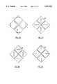
- FIG. 14shows the foursquare antenna element with all of the corners of it petals 60 trimmed.
- the dashed lines 62illustrate the trimmed portion.
- both pair of feeds 64 and 64'are feed, the frequency response of both polarizations will be modified. It is theorized that the frequency response will improve with trimming.
- FIG. 15shows trimming taken to the extreme where the entire corner of the petal 60 is trimmed.
- FIGS. 16 and 17Similar to FIGS. 16 and 17 shows rounded outer petal corners 66 of the trimmed foursquare antenna element. This is theorized to have an effect on the frequency response. In practice all of the elements may have ever so slightly rounded corners due manufacturing tolerances. FIG. 17 shows that in the extreme case of round trimming the corners which results in a circular element. While circular elements have the disadvantage that they do not fit together nicely in an array, there should be less capacitive coupling between the edges of circular elements which is an advantage.
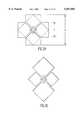
- FIGS. 18-21show various trimming configurations where other than the outer corners of the foursquare element are trimmed.
- FIG. 18shows adjacent sides, 70 and 72, of the individual petals 68 are trimmed, This results in irregular spacing between the individual petals 68.
- FIG. 19shows the corners 76 and 78 perpendicular to the feed points 74 trimmed.
- FIG. 20shows the inner petal corners 80 near the feed points 82 trimmed.
- FIG. 21shows a configuration having only two opposing corners 84 and 86 trimmed.
- FIG. 22shows a trimmed foursquare with a concave 88 curvature on the sides. This configuration would have the beneficial effect in an array of reducing the coupling between adjacent elements. This could also be used to optimize the frequency response of an individual element.
- FIG. 23shows a trimmed foursquare where the gaps 90 in the element are generally curved instead of straight.
- the gaps 90could be made in a zig zag or meandering pattern. This would have the effect of increasing the capacitance between the petals.
- FIGS. 25-29show the foursquare element having slots trimmed into the petals.
- the slotsmay be circular 92.
- the slotsmay be longitudinal 94 and may be located in a variety of locations on the petals.
- the slots in the petal metalcontrol the way the current flows to modify the performance parameters and improve the frequency response of the antenna.
- FIGS. 30-32show placing notches in the edge of the petals to modify its shape.
- the notchesare similar in idea to the slots shown above in FIGS. 25-29.
- the purpose of the notchesis to control the flow of current to improve the frequency response of the element.
- FIG. 35shows a variation of the foursquare antenna where the pairs of radiating elements are different sizes since the outer sides of one pair of radiating elements have been trimmed. This arrangement also allows for a greater size in the vertical dimension.
Landscapes
- Variable-Direction Aerials And Aerial Arrays (AREA)
- Waveguide Aerials (AREA)
Abstract
Description
This application is a continuation-in-part (CIP) of U.S. application Ser. No. 08/885,837, filed on Jun. 30, 1997, now U.S. Pat. No. 5,926,137, herein incorporated by reference.
1. Field of the Invention
The present invention generally relates to an antenna radiating element and, more particularly, to a foursquare antenna element which can provide dual polarization useful in, for example, compact, wideband radar and communication antenna arrays.
2. Description of the Related Art
An antenna is a transducer between free space propagation and guided wave propagation of electromagnetic waves. During a transmission, the antenna concentrates radiated energy into a shaped directive beam which illuminates targets in a desired direction. In a radar system, the target is some physical object, the presence of which is to be determined. In a communication system, the target may be a receiving antenna.
During reception, the antenna collects energy from the free space propagation. In a radar system, this energy comprises a signal reflected back to the antenna from a target. Hence, in a radar system, a single antenna may be used to both transmit and receive signals. Likewise in a communication system an antenna may serve the dual functions of transmitting and receiving signals from a remote antenna. In a radar system, the primary purpose of the antenna is to determine the angular direction of the target. A highly directive, narrow beam-width is needed in order to accurately determine angular direction as well as to resolve multiple targets in physically close proximity to one another.
Phased array antenna systems are formed from an arrayed combination of multiple, individual, similar radiator elements. The phased array antenna characteristics are determined by the geometry and the relative positioning of the individual elements and the phase and amplitude of their excitation. The phased array antenna aperture is assembled from the individual radiating elements, such as, for example, dipoles or slots. By individually controlling the phase and amplitude of the elements very predictable radiation patterns and beam directions can be realized. The antenna aperture refers to the physical area projected on a plane perpendicular to the main beam direction. Briefly, there are several important parameters which govern antenna performance. These include the radiation pattern (including polarization), gain, and the antenna impedance.
The radiation pattern refers to the electromagnetic energy distribution in three-dimensional angular space. When normalized and plotted, it is referred to as the antenna radiation pattern. The direction of polarization of an antenna is defined as the direction of the electric field (E-field) vector. Typically, a radar antenna is linearly polarized, in either the horizontal or the vertical direction using earth as a reference. However, circular and elliptical polarizations are also common. In circular polarization, the E-field varies with time at any fixed observation point, tracing a circular locus once per RF (radio frequency) cycle in a fixed plane normal to the direction of propagation. Circular polarization is useful, for example, to detect aircraft targets in the rain. Similarly, elliptical polarization traces an elliptical locus once per RF cycle.
Gain comprises directive gain (referred to as "directivity" GD) and power gain (referred to as simply "gain" G) and relates to the ability of the antenna to concentrate energy in a narrow angular regions. Directive gain, or directivity, is defined as the maximum beam radiation intensity relative to the average intensity, usually given in units of watts per steradian. Directional gain may also be expressed as maximum radiated power density (i.e., watts/meter2) at a far field distance R relative to the average density at the same distance. Power gain, or simply gain, is defined as power accepted at by the antenna input port, rather than radiated power. The directivity gain and the power gain are related by the radiation efficiency factor of the antenna. For an ideal antenna, with a radiation efficiency factor of 1, the directional gain and the power gain are the same (i.e., G=GD).
Antenna input impedance is made up of the resistive and reactive components presented at the antenna feed. The resistive component is the result of antenna radiation and ohmic losses. The reactive component is the result of stored energy in the antenna. In broad band antennas it is desirable for the resistive component to be constant with frequency and have a moderate value (50 Ohms, for example). The magnitude of the reactive component should be small (ideally zero). For most antennas the reactive component is small over a limited frequency range.
Phased array antennas capable of scanning have been know for some time. However, phased array antennas have had a resurgence for modem applications with the introduction of electronically controlled phase shifters and switches. Electronic control allows aperture excitement to be modulated by controlling the phase of the individual elements to realize beams that are scanned electronically. General information on phased array antennas and scanning principles can be gleaned from Merrill Skolnik, Radar Handbook, second edition, McGraw-Hill, 1990, herein incorporated by reference. Phased array antennas lend themselves particularly well to radar and directional communication applications.
Since the impedance and radiation pattern of a radiator in an array are determined predominantly by the array geometry, the radiating element should be chosen to suit the feed system and the physical requirements of the antenna. The most commonly used radiators for phased arrays are dipoles, slots, open-ended waveguides (or small horns), and printed-circuit "patches". The element has to be small enough to fit in the array geometry, thereby limiting the element to an area of a little more than λ/4, where λ is wavelength. In addition, since the antenna operates by aggregating the contribution of each small radiator element at a distance, many radiators are required for the antenna to be effective. Hence, the radiating element should be inexpensive and reliable and have identical, predictable characteristics from unit to unit.
Radiator elements such as the "four arm sinuous log-periodic", described in U.S. Pat. No. 4,658,262 to DuHamel, and the Archaemedian spiral, which have wide bandwidths and are otherwise desirable for array applications have diameters greater than 0.43 λ at their lowest frequency. With a bandwidth in excess of 1.5:1 in a square grid array an interelement spacing of about 0.33 λ is desired.
It is therefore an object of the present invention to provide an antenna radiating element which is suitable for use in radar and communication applications.
It is yet another object of the present invention to provide a foursquare dual polarized radiating element having a wide bandwidth.
It is yet another object of the present invention to provide an antenna element that is smaller than other antenna elements having the same low frequency response and therefore can be placed closer to other elements in an array.
According to the invention, a foursquare dual polarized moderately wide bandwidth antenna radiating element is provided which, due to its small size and low frequency response, is well suited to array applications. The foursquare element comprises a printed metalization on a low-loss substrate suspended over a ground plane reflector. Dual linear (i.e., horizontal and vertical), as well as circular and elliptical polarizations of any orientation may be produced with the inventive foursquare element. Further, an array of such elements can be modulated to produce a highly directive beam which can be scanned by adjusting the relative phase of the elements. Operation of the array is enhanced because the individual foursquare elements are small as compared to conventional array element having comparable frequency response. The small size allows for closer spacing of the individual elements which facilitates scanning. Bandwidths of 1.5:1 or better may be obtained with a feed point impedance of 50 Ohms. Good performance is obtained with the foursquare element having a size between 0.30 λ and 0.40 λ and preferably of 0.36 λ. Also the foursquare element impedance degrades gradually in contrast to some elements such as the "four arm sinuous log-periodic" which has large impedance variations near its lowest frequency.
The foregoing and other objects, aspects and advantages will be better understood from the following detailed description of a preferred embodiment of the invention with reference to the drawings, in which:
FIGS. 1A and 1B is a top view, and a cross-sectional view of the foursquare element according to the present invention, respectively;
FIG. 2 is a perspective view foursquare antenna element;
FIG. 3 is a top view of the foursquare antenna element showing the feed points for various polarizations;
FIG. 4 is a feed point impedance plot for the foursquare antenna element;
FIG. 5 is a mid-band E plane radiation pattern for the foursquare element;
FIG. 6 is a mid-band H plane radiation pattern for the foursquare element;
FIG. 7 is an illustrative geometry of a fully array comprised of many foursquare elements;
FIG. 8 is a top view of a second embodiment of the present invention comprising a trimmed four-square antenna element configuration;
FIG. 9 is a cross-sectional view of the trimmed four-square antenna element;
FIG. 10 is a top view showing the geometry of the trimmed four-square antenna element;
FIG. 11 is an E-plane co-polarized pattern of the trimmed foursquare for midband;
FIG. 12 is an H-plane co-polarized pattern of the trimmed foursquare for midband;
FIG. 13 is a graph showing the trimmed four-square input impedance; and
FIGS. 14-35 show various alternative embodiments comprising different ways of trimming the basic foursquare antenna as described above.
Referring now to the drawings, and more particularly to FIGS. 1A and 1B, there is shown a top view of thefoursquare element 10 according to the present invention, and a cross sectional view taken along line A--A', respectively. Thefoursquare element 10 comprises a four smallsquare metalization regions low loss substrate 20. Thelow loss substrate 20 may be secured to a ground plane. Each of the smallsquare regions foursquare element 10 can therefore be used to produce dual linear (i.e., vertical or horizontal polarization) or circular polarization of either sense similar to crossed dipoles. Appropriate feeding of the crossed element in the foursquare antenna can be used to produce various angles of linear or elliptical polarization.
For example, linear polarization may be obtained by feeding either element half (e.g., 12 and 18, or 14 and 16) diagonally across the gap W'. In this case the polarization will be in line with the diagonal of the feed. Other linear polarizations may be obtained by feeding both element halves in phase with one another. The angle of the polarization is determined by the relative amplitude of the sources. Circular polarization is obtained by feeding the crossed element halves in phase quadrature (i.e. 90 degree relationship) and equal amplitude.
Thefoursquare element 10 of the present invention can be arranged into an array to produce a highly directive beam. The array beam can then be scanned by adjusting the relative phase of the elements according to conventional practice. Thefoursquare element 10 has the advantage of allowing relatively close spacing of adjacent elements, by arranging the elements so that the element sides are parallel to one another. When the elements are placed in this manner the principal polarization planes are diagonal to the sides of the array. If other polarization orientations are desired the array can be rotated. By applying excitation to the crossed element pairs (12 and 18, or 14 and 16) with equal and in-phase currents, a composite polarization oriented along the side of the elements and the array is produced. Other polarizations are produced in a similar manner.
The frequency range of thefoursquare element 10 is limited to less than a 2:1 range by the low input resistance, increasing capacitive reactance at the lowest operating frequency, and by the rapid rise in impedance or anti-resonance which occurs at the high frequency end.
Some narrow band applications may be able to extend the low frequency response by use of conventional matching techniques. The lowest frequency of operation for the element occurs when the diagonal of the square element is approximately 1/2 wavelength (λ/2). The anti-resonance which limits the high frequency response occurs when the diagonal D across theelement 10 becomes approximately one wavelength (D≈λ). The anti-resonance may not be approached closely however because of the rapidly increasing reactance. An early test element placed over a ground plane gave a bandwidth of about 1.5:1 with the limits taken at a voltage standing wave ratio (vswr) of 2. This bandwidth would be typical of an uncompensated foursquare element.
FIG. 2 shows a perspective view of the foursquare element according to the present invention superimposed on a Cartesian origin. The perspective view is shown in wire grid representation for illustrative purposes; however, typically the elements would be solid printed metalizations. Theground plane 22 lies parallel to the x-y plane and parallel to the plane of theelements
FIG. 3 shows a top view of the foursquare element according to the present invention. As shown, the size of the diagonal D across theelement 10 is approximately λ/2 at the lowest frequency. The gap W between the metalizedregions
Referring back to FIGS. 1A and 1B, by way of example, a prototype has been built for the four square element having an overall element width of C=0.86 inches, a metalization width of L=0.84 inches, a gap width W=0.01 inches, and a ground plane spacing H=0.278 inches. Thesubstrate 20 was a layered composite material consisting of an upper layer of glass microfiber reinforced polytetrafluoroethylene, such as RT/duroid® 5870 having a thickness of 0.028 inches with 1 oz. copper cladding and a lower layer of polystyrene foam having a thickness of 0.250 inches. The four metalizedregions
A foursquare element has also been constructed on asolid substrate 20 of polystyrene cross linked with divinylbenzene, such as Rexolite®. Another possible construction is a substrate of solid polystyrene foam or polyethylene foam withmetal tape elements metalization regions ground plane 22 with dielectric standoffs.
FIG. 4 shows the feed point impedance plot for the foursquare element above. This plot demonstrates the broad band nature of the element. The gradual decline of the real component toward the lower end of the frequency range as well as the rise in reactance on the high frequency end represents the limitation in frequency response of the element.
FIGS. 5 and 6 are the mid-band E and H plane radiation patterns for the four square element, respectively. Both planes demonstrate the clean wide beam pattern required for phased array applications. Other frequencies in the element pass band show similar radiation patterns.
FIG. 7 is an illustrative geometry of a full array comprised of many foursquare elements. This particular array geometry is suitable for use in a radar system. Each small square represents an individual foursquare element. Each foursquare element has an individual set of feed lines and phase shifters. The foursquare elements, feed lines and phase shifters are the connected via acorporate feed controller 30 to transmitting and receiving systems. By adjusting the phase shifters the direction of the beam is scanned.
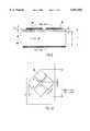
FIG. 8 shows a top view of a second embodiment of the present invention comprising a trimmed four-square configuration 40. The basic construction of the trimmed four-square is the same as thefoursquare element 42 described above except that the ends or outer corners of one pair of plates, 44 and 44', are trimmed.
The overall size of an array element is determined by the frequency of operation. In an array of radiating elements the spacing between elements is determined by array geometry and other parameters which usually require elements to be closely packed together. These parameters often conflict in array design. The trimmedfoursquare element 40 is useful for array requirements in which the broad frequency bandwidth characteristics of thefoursquare element 42 are desired but the dimensions allowed by the array geometry were insufficient to accommodate the element in one dimension.
Still referring to FIG. 8,configuration 42 is a foursquare element as described above. The trimmedconfiguration 40; however, allows for a greater size in the vertical dimension. This arrangement allows the frequency of operation of the trimmed to be lower than with then with theuntrimmed foursquare antenna 42. The drawback is that only the vertical polarization is supported without compromise. Some use may be made of the horizontal portion of the element if reduced frequency coverage is accepted. In the vertical polarization the trimmed foursquare has 40 a frequency response equal to or better than thefoursquare element 42. The radiation patterns and gain characteristics are also equal to the conventional element.
In a tested example as described below, the reduction in the horizontal dimension is approximately 15%. Reductions in the horizontal dimension of 25% or even 50% should also be possible. Details of the Trimmed Foursquare construction are shown in FIGS. 9 and 10. A summary of the parameter values is given in Table 1. The primary design guidelines are as follows:
1) Select thesubstrate 46 anddielectric foam 48 thickness so that themetallization 50 is approximately a quarter-wavelength (at the high frequency) above the ground plane (h=0.25 λ).
2) Print themetallization 50 on the substrate so that the diagonal distance (D) is approximately one half-wavelength (at the low frequency).
3) Feed the foursquare element so that F is as small as physically possible (ideally, F=W').
4) The input impedance of the foursquare element is partially determined by the gap width W. The gap is similar to a slotline transmission line.
The parasitic (undriven) arms of an untrimmed foursquare are identical to the driven arms. In this application the parasitic arms extended beyond the element extents. Therefore, it was necessary to trim the parasitic arms. This was done in order to fit the element in the array lattice. Since the element is only being excited for linear polarization, this trimming does not adversely affect the performance of the element.
______________________________________ Parameter Symbol Quantity ______________________________________ diagonal distance D ≈ 1/2 wavelength at min. frequency distance between feed points F 0.086 inchesgap width W 10 mils diagonal gap width W' 14.142 mils thickness of metallization t.sub.m e.g. 1 oz. Copper thickness of substrate t.sub.s 28 mils (e.g. Duroid ®) thickness of dielectric foam t.sub.d h-t.sub.s height above ground plane h ≈ 1/4 wavelength at max. frequencytrim margin t 10 mils ______________________________________
Of course it is understood that the above parameters are offered as an example and should not be taken to limit the invention in any manner.
E-plane and H-plane co-polarized patterns of the trimmed foursquare for midband are shown in FIGS. 11 and 12, respectively. Additionally, the patterns are approximated using a cosq (θ) pattern (for 0<0<90°). The approximated patterns are plotted along with the measured data. The value for q is calculated using ##EQU1##
where θ is taken at the -10 dB points. The cosq (θ) pattern assumes no backplane radiation. Therefore, it should overestimate the directivity slightly.
As shown in FIG. 13 the impedance characteristics of the trimmed foursquare antenna are equal to or better than the untrimmed version.
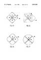
FIGS. 14-33 show various alternative embodiments comprising different ways of trimming the basic foursquare antenna as described above. The individual elements in all of the variations retain at least two perpendicular sides owing to its model square shape.
FIG. 14 shows the foursquare antenna element with all of the corners of itpetals 60 trimmed. The dashedlines 62 illustrate the trimmed portion. When both pair offeeds 64 and 64' are feed, the frequency response of both polarizations will be modified. It is theorized that the frequency response will improve with trimming. FIG. 15 shows trimming taken to the extreme where the entire corner of thepetal 60 is trimmed.
Similar to FIGS. 16 and 17 shows roundedouter petal corners 66 of the trimmed foursquare antenna element. This is theorized to have an effect on the frequency response. In practice all of the elements may have ever so slightly rounded corners due manufacturing tolerances. FIG. 17 shows that in the extreme case of round trimming the corners which results in a circular element. While circular elements have the disadvantage that they do not fit together nicely in an array, there should be less capacitive coupling between the edges of circular elements which is an advantage.
FIGS. 18-21 show various trimming configurations where other than the outer corners of the foursquare element are trimmed. FIG. 18 shows adjacent sides, 70 and 72, of theindividual petals 68 are trimmed, This results in irregular spacing between theindividual petals 68. FIG. 19 shows thecorners inner petal corners 80 near the feed points 82 trimmed. FIG. 21 shows a configuration having only two opposingcorners
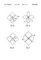
FIG. 22 shows a trimmed foursquare with a concave 88 curvature on the sides. This configuration would have the beneficial effect in an array of reducing the coupling between adjacent elements. This could also be used to optimize the frequency response of an individual element.
FIG. 23 shows a trimmed foursquare where thegaps 90 in the element are generally curved instead of straight. Similarly, in FIG. 24, thegaps 90 could be made in a zig zag or meandering pattern. This would have the effect of increasing the capacitance between the petals.
FIGS. 25-29 show the foursquare element having slots trimmed into the petals. As shown in FIG. 25, the slots may be circular 92. As shown in FIGS. 26-29, the slots may be longitudinal 94 and may be located in a variety of locations on the petals. Here, the slots in the petal metal control the way the current flows to modify the performance parameters and improve the frequency response of the antenna.
FIGS. 30-32 show placing notches in the edge of the petals to modify its shape. The notches are similar in idea to the slots shown above in FIGS. 25-29. The purpose of the notches is to control the flow of current to improve the frequency response of the element.
FIG. 33 extends the trimmed foursquare by adding metal to the active petals of the element so that the element becomes rectangular in shape. Better performance over the trimmed foursquare shown in FIG. 8 is expected. The element will take up slightly more area than the trimmed foursquare for the same operating frequency range. Similarly, FIG. 34 shows a "fat-cross" foursquare antenna configuration. Note that the length to width ratio is 2, that is, D/E=2. Thus this ratio is the same as the original foursquare design as illustrated by the dashed lines therefore similar performance is expected.
FIG. 35 shows a variation of the foursquare antenna where the pairs of radiating elements are different sizes since the outer sides of one pair of radiating elements have been trimmed. This arrangement also allows for a greater size in the vertical dimension.
While the invention has been described in terms of a several preferred embodiments, those skilled in the art will recognize that the invention can be practiced with modification within the spirit and scope of the appended claims.
Claims (13)
1. An antenna element, comprising:
a dielectric layer;
four radiating elements comprising two pairs positioned over a top side of said dielectric layer, said pairs positioned diagonal to each other,
a first of said pairs comprising square radiating elements and a second of said pairs comprising square radiating elements each having at least one corner trimmed; and
at least two feed points located near an inner corner of one of said first and second pairs.
2. An antenna element as recited in claim 1 wherein said outer corner is round trimmed.
3. An antenna element as recited in claim 1 wherein said square radiating elements of said first pair comprises at least one trimmed corner.
4. An antenna element as recited in claim 1 further comprising a ground plane positioned under said dielectric layer, wherein a spacing between said ground plane and said radiating elements is approximately one fourth of a wavelength at a maximum frequency.
5. An antenna element as recited in claim 1 wherein two feed lines connect to said two feed points and extend through vias in said dielectric layer.
6. An antenna element as recited in claim 1 wherein said four radiating elements are separated from adjacent ones of said four radiating elements by a distance W and wherein a diagonal D across said pairs is approximately one-half wavelength at a lowest operating frequency.
7. An antenna element, comprising:
a dielectric layer;
four radiating elements comprising two pairs positioned over a top side of said dielectric layer, said pairs positioned diagonal to each other,
a first of said pairs comprising radiating elements each having at least two perpendicular sides and a second of said pairs comprising at least two radiating elements each having at least two perpendicular sides; and
at least two feed points located near an inner portion of one of said first and second pairs.
8. An antenna element, comprising:
a dielectric layer;
four quadrilateral radiating elements comprising two pairs positioned on a top side of said dielectric layer, said pairs positioned diagonal to each other;
four feed lines, one of said four feed connecting to a feed point on a corresponding one of said four quadrilateral radiating elements; and
a slot positioned on each of said four quadrilateral radiating elements.
9. An antenna element as recited in claim 8 wherein said slot is circular.
10. An antenna element as recited in claim 8 wherein said slot is longitudinal.
11. A scannable array of radiating elements, comprising:
a plurality radiating elements arranged in a geometrically shaped array; and
controller means for controlling a phase and amplitude of feeds to each of said radiating elements, each of said radiating elements comprising:
four metalized radiating elements arranged in a foursquare pattern, each of said four metalized radiating elements having at least two perpendicular sides; and
at least one pair of feed points, connected to opposing ones of said four metalized radiating elements.
12. A scannable array of radiating elements as recited in claim 11 wherein each of said radiating elements further comprises:
a dielectric layer beneath said metalized radiating elements,
a ground plane beneath said dielectric layer; and
vias through said dielectric layer to connect said feeds to said feed points.
13. A scannable array of radiating elements as recited in claim 11 wherein each of said radiating elements is comprise at least one square corner.
Priority Applications (3)
| Application Number | Priority Date | Filing Date | Title |
|---|---|---|---|
| US09/326,688US6057802A (en) | 1997-06-30 | 1999-06-07 | Trimmed foursquare antenna radiating element |
| PCT/US2000/013962WO2000076029A1 (en) | 1999-06-07 | 2000-05-22 | Trimmed foursquare antenna radiating element |
| AU52787/00AAU5278700A (en) | 1999-06-07 | 2000-05-22 | Trimmed foursquare antenna radiating element |
Applications Claiming Priority (2)
| Application Number | Priority Date | Filing Date | Title |
|---|---|---|---|
| US08/885,837US5926137A (en) | 1997-06-30 | 1997-06-30 | Foursquare antenna radiating element |
| US09/326,688US6057802A (en) | 1997-06-30 | 1999-06-07 | Trimmed foursquare antenna radiating element |
Related Parent Applications (1)
| Application Number | Title | Priority Date | Filing Date |
|---|---|---|---|
| US08/885,837Continuation-In-PartUS5926137A (en) | 1997-06-30 | 1997-06-30 | Foursquare antenna radiating element |
Publications (1)
| Publication Number | Publication Date |
|---|---|
| US6057802Atrue US6057802A (en) | 2000-05-02 |
Family
ID=23273254
Family Applications (1)
| Application Number | Title | Priority Date | Filing Date |
|---|---|---|---|
| US09/326,688Expired - Fee RelatedUS6057802A (en) | 1997-06-30 | 1999-06-07 | Trimmed foursquare antenna radiating element |
Country Status (3)
| Country | Link |
|---|---|
| US (1) | US6057802A (en) |
| AU (1) | AU5278700A (en) |
| WO (1) | WO2000076029A1 (en) |
Cited By (177)
| Publication number | Priority date | Publication date | Assignee | Title |
|---|---|---|---|---|
| US6281846B1 (en)* | 1998-05-06 | 2001-08-28 | Universitat Politecnica De Catalunya | Dual multitriangular antennas for GSM and DCS cellular telephony |
| RU2195056C2 (en)* | 2000-12-15 | 2002-12-20 | Открытое акционерное общество "МЕТЕО" | Circularly and linearly polarized antenna system of weather radar |
| WO2002041443A3 (en)* | 2000-10-31 | 2002-12-27 | Harris Corp | Wideband phased array antenna and associated methods |
| WO2003021717A1 (en)* | 2001-08-31 | 2003-03-13 | The Trustees Of Columbia University In The City Of New York | Systems and methods for providing optimized patch antenna excitation for mutually coupled patches |
| WO2003050917A1 (en)* | 2001-12-07 | 2003-06-19 | Skycross, Inc. | Multiple antenna diversity for wireless lan applications |
| US20030210207A1 (en)* | 2002-02-08 | 2003-11-13 | Seong-Youp Suh | Planar wideband antennas |
| US20040012530A1 (en)* | 2002-04-19 | 2004-01-22 | Li Chen | Ultra-wide band meanderline fed monopole antenna |
| US20040027286A1 (en)* | 2001-06-26 | 2004-02-12 | Gregory Poilasne | Multi frequency magnetic dipole antenna structures and methods of reusing the volume of an antenna |
| WO2004019450A1 (en)* | 2002-08-22 | 2004-03-04 | Skycross, Inc. | Apparatus and method for forming a monolithic surface-mountable antenna |
| US20040090389A1 (en)* | 2002-08-19 | 2004-05-13 | Young-Min Jo | Compact, low profile, circular polarization cubic antenna |
| US20040125020A1 (en)* | 2002-06-04 | 2004-07-01 | Hendler Jason M. | Wideband printed monopole antenna |
| US20040155831A1 (en)* | 2002-12-23 | 2004-08-12 | Huberag | Broadband antenna having a three-dimensional cast part |
| US20040217910A1 (en)* | 2003-02-13 | 2004-11-04 | Mark Montgomery | Monolithic low profile omni-directional surface-mount antenna |
| EP1466386A4 (en)* | 2002-01-17 | 2005-04-27 | Harris Corp | Enhanced bandwidth dual layer current sheet antenna |
| US20050270238A1 (en)* | 2004-06-08 | 2005-12-08 | Young-Min Jo | Tri-band antenna for digital multimedia broadcast (DMB) applications |
| US20060017620A1 (en)* | 2002-04-19 | 2006-01-26 | Li Chen | Ultra-wide band meanderline fed monopole antenna |
| EP1777780A3 (en)* | 2002-01-17 | 2007-05-16 | Harris Corporation | Enhanced bandwidth single layer current sheet antenna |
| US20070109194A1 (en)* | 2005-11-15 | 2007-05-17 | Clearone Communications, Inc. | Planar anti-reflective interference antennas with extra-planar element extensions |
| US20070111749A1 (en)* | 2005-11-15 | 2007-05-17 | Clearone Communications, Inc. | Wireless communications device with reflective interference immunity |
| US20070109193A1 (en)* | 2005-11-15 | 2007-05-17 | Clearone Communications, Inc. | Anti-reflective interference antennas with radially-oriented elements |
| US20080218424A1 (en)* | 2005-10-14 | 2008-09-11 | Blanton James L | Device and method for polarization control for a phased array antenna |
| US20090160697A1 (en)* | 2007-12-20 | 2009-06-25 | Honeywell International, Inc. | System and method for reducing interference in microwave motion sensors |
| US20090160730A1 (en)* | 2007-12-21 | 2009-06-25 | Alcatel-Lucent | Dual polarised radiating element for cellular base station antennas |
| EP2159875A1 (en)* | 2008-08-28 | 2010-03-03 | Thales Nederland B.V. | An array antenna comprising means to suppress the coupling effect in the dielectric gaps between its radiator elements without establishing galvanic contacts |
| US20100177002A1 (en)* | 2009-01-10 | 2010-07-15 | Arcadyan Technology Corporation | Dipole antenna |
| CN101783442A (en)* | 2009-01-16 | 2010-07-21 | 智易科技股份有限公司 | Dipole antenna |
| GB2469075A (en)* | 2009-03-31 | 2010-10-06 | Univ Manchester | Wide band array antenna |
| WO2011025713A1 (en)* | 2009-08-28 | 2011-03-03 | Svr, Inventions, Inc. D/B/A Svr Inventions Corporation | Planar antenna array and article of manufacture using same |
| WO2011064586A1 (en)* | 2009-11-27 | 2011-06-03 | Bae Systems Plc | Antenna array |
| WO2011064585A1 (en)* | 2009-11-27 | 2011-06-03 | Bae Systems Plc | Antenna array |
| EP2343775A1 (en)* | 2009-11-27 | 2011-07-13 | BAE Systems PLC | Antenna array |
| CN103367897A (en)* | 2013-07-10 | 2013-10-23 | 电子科技大学 | Small-sized highly-insulated broadband dual-polarization printed dipole antenna |
| US20140176386A1 (en)* | 2012-12-20 | 2014-06-26 | Deere & Company | Antenna for a satellite navigation receiver |
| TWI475749B (en)* | 2010-12-30 | 2015-03-01 | Tai Saw Technology Co Ltd | Modified antenna |
| US20150226846A1 (en)* | 2014-02-12 | 2015-08-13 | Battelle Memorial Institute | Shared aperture antenna array |
| KR20160000770A (en)* | 2014-06-25 | 2016-01-05 | 주식회사 감마누 | Broadband Dual-polarized dipole antenna by multipath |
| US20160190869A1 (en)* | 2014-12-29 | 2016-06-30 | Shuai SHAO | Reconfigurable reconstructive antenna array |
| KR101652284B1 (en)* | 2015-12-01 | 2016-08-30 | 주식회사 감마누 | Radiating element and Base station antenna using thereof |
| KR101709318B1 (en)* | 2016-06-23 | 2017-02-23 | 주식회사 감마누 | Radiating element and Base station antenna using thereof |
| GB2544558A (en)* | 2015-11-23 | 2017-05-24 | Mannan Michael | Low profile antenna with high gain |
| US9667317B2 (en) | 2015-06-15 | 2017-05-30 | At&T Intellectual Property I, L.P. | Method and apparatus for providing security using network traffic adjustments |
| US9674711B2 (en) | 2013-11-06 | 2017-06-06 | At&T Intellectual Property I, L.P. | Surface-wave communications and methods thereof |
| US9685992B2 (en) | 2014-10-03 | 2017-06-20 | At&T Intellectual Property I, L.P. | Circuit panel network and methods thereof |
| US9705610B2 (en) | 2014-10-21 | 2017-07-11 | At&T Intellectual Property I, L.P. | Transmission device with impairment compensation and methods for use therewith |
| US9705561B2 (en) | 2015-04-24 | 2017-07-11 | At&T Intellectual Property I, L.P. | Directional coupling device and methods for use therewith |
| US9722318B2 (en) | 2015-07-14 | 2017-08-01 | At&T Intellectual Property I, L.P. | Method and apparatus for coupling an antenna to a device |
| US9729197B2 (en) | 2015-10-01 | 2017-08-08 | At&T Intellectual Property I, L.P. | Method and apparatus for communicating network management traffic over a network |
| US9735833B2 (en) | 2015-07-31 | 2017-08-15 | At&T Intellectual Property I, L.P. | Method and apparatus for communications management in a neighborhood network |
| US9742521B2 (en) | 2014-11-20 | 2017-08-22 | At&T Intellectual Property I, L.P. | Transmission device with mode division multiplexing and methods for use therewith |
| US9742462B2 (en) | 2014-12-04 | 2017-08-22 | At&T Intellectual Property I, L.P. | Transmission medium and communication interfaces and methods for use therewith |
| US9749013B2 (en) | 2015-03-17 | 2017-08-29 | At&T Intellectual Property I, L.P. | Method and apparatus for reducing attenuation of electromagnetic waves guided by a transmission medium |
| US9749053B2 (en) | 2015-07-23 | 2017-08-29 | At&T Intellectual Property I, L.P. | Node device, repeater and methods for use therewith |
| US9748626B2 (en) | 2015-05-14 | 2017-08-29 | At&T Intellectual Property I, L.P. | Plurality of cables having different cross-sectional shapes which are bundled together to form a transmission medium |
| US9769020B2 (en) | 2014-10-21 | 2017-09-19 | At&T Intellectual Property I, L.P. | Method and apparatus for responding to events affecting communications in a communication network |
| US9769128B2 (en) | 2015-09-28 | 2017-09-19 | At&T Intellectual Property I, L.P. | Method and apparatus for encryption of communications over a network |
| US9768833B2 (en) | 2014-09-15 | 2017-09-19 | At&T Intellectual Property I, L.P. | Method and apparatus for sensing a condition in a transmission medium of electromagnetic waves |
| US9780834B2 (en) | 2014-10-21 | 2017-10-03 | At&T Intellectual Property I, L.P. | Method and apparatus for transmitting electromagnetic waves |
| US9787412B2 (en) | 2015-06-25 | 2017-10-10 | At&T Intellectual Property I, L.P. | Methods and apparatus for inducing a fundamental wave mode on a transmission medium |
| US9793951B2 (en) | 2015-07-15 | 2017-10-17 | At&T Intellectual Property I, L.P. | Method and apparatus for launching a wave mode that mitigates interference |
| US9793955B2 (en) | 2015-04-24 | 2017-10-17 | At&T Intellectual Property I, Lp | Passive electrical coupling device and methods for use therewith |
| US9793954B2 (en) | 2015-04-28 | 2017-10-17 | At&T Intellectual Property I, L.P. | Magnetic coupling device and methods for use therewith |
| US9800327B2 (en) | 2014-11-20 | 2017-10-24 | At&T Intellectual Property I, L.P. | Apparatus for controlling operations of a communication device and methods thereof |
| US20170310016A1 (en)* | 2014-10-21 | 2017-10-26 | Nec Corporation | Planar antenna |
| US9820146B2 (en) | 2015-06-12 | 2017-11-14 | At&T Intellectual Property I, L.P. | Method and apparatus for authentication and identity management of communicating devices |
| US9838896B1 (en) | 2016-12-09 | 2017-12-05 | At&T Intellectual Property I, L.P. | Method and apparatus for assessing network coverage |
| US9838078B2 (en) | 2015-07-31 | 2017-12-05 | At&T Intellectual Property I, L.P. | Method and apparatus for exchanging communication signals |
| US9847850B2 (en) | 2014-10-14 | 2017-12-19 | At&T Intellectual Property I, L.P. | Method and apparatus for adjusting a mode of communication in a communication network |
| US9847566B2 (en) | 2015-07-14 | 2017-12-19 | At&T Intellectual Property I, L.P. | Method and apparatus for adjusting a field of a signal to mitigate interference |
| US9853342B2 (en) | 2015-07-14 | 2017-12-26 | At&T Intellectual Property I, L.P. | Dielectric transmission medium connector and methods for use therewith |
| US9860075B1 (en) | 2016-08-26 | 2018-01-02 | At&T Intellectual Property I, L.P. | Method and communication node for broadband distribution |
| US9865911B2 (en) | 2015-06-25 | 2018-01-09 | At&T Intellectual Property I, L.P. | Waveguide system for slot radiating first electromagnetic waves that are combined into a non-fundamental wave mode second electromagnetic wave on a transmission medium |
| US9866276B2 (en) | 2014-10-10 | 2018-01-09 | At&T Intellectual Property I, L.P. | Method and apparatus for arranging communication sessions in a communication system |
| US9866309B2 (en) | 2015-06-03 | 2018-01-09 | At&T Intellectual Property I, Lp | Host node device and methods for use therewith |
| US20180013210A1 (en)* | 2016-07-07 | 2018-01-11 | Elta Systems Ltd. | System and method for operating conformal antenna |
| US9871282B2 (en) | 2015-05-14 | 2018-01-16 | At&T Intellectual Property I, L.P. | At least one transmission medium having a dielectric surface that is covered at least in part by a second dielectric |
| US9871558B2 (en) | 2014-10-21 | 2018-01-16 | At&T Intellectual Property I, L.P. | Guided-wave transmission device and methods for use therewith |
| US9871283B2 (en) | 2015-07-23 | 2018-01-16 | At&T Intellectual Property I, Lp | Transmission medium having a dielectric core comprised of plural members connected by a ball and socket configuration |
| US9876605B1 (en) | 2016-10-21 | 2018-01-23 | At&T Intellectual Property I, L.P. | Launcher and coupling system to support desired guided wave mode |
| US9876571B2 (en) | 2015-02-20 | 2018-01-23 | At&T Intellectual Property I, Lp | Guided-wave transmission device with non-fundamental mode propagation and methods for use therewith |
| US9876264B2 (en) | 2015-10-02 | 2018-01-23 | At&T Intellectual Property I, Lp | Communication system, guided wave switch and methods for use therewith |
| US9882257B2 (en) | 2015-07-14 | 2018-01-30 | At&T Intellectual Property I, L.P. | Method and apparatus for launching a wave mode that mitigates interference |
| US9887447B2 (en) | 2015-05-14 | 2018-02-06 | At&T Intellectual Property I, L.P. | Transmission medium having multiple cores and methods for use therewith |
| US9893795B1 (en) | 2016-12-07 | 2018-02-13 | At&T Intellectual Property I, Lp | Method and repeater for broadband distribution |
| US9906269B2 (en) | 2014-09-17 | 2018-02-27 | At&T Intellectual Property I, L.P. | Monitoring and mitigating conditions in a communication network |
| US9904535B2 (en) | 2015-09-14 | 2018-02-27 | At&T Intellectual Property I, L.P. | Method and apparatus for distributing software |
| US9912033B2 (en) | 2014-10-21 | 2018-03-06 | At&T Intellectual Property I, Lp | Guided wave coupler, coupling module and methods for use therewith |
| US9913139B2 (en) | 2015-06-09 | 2018-03-06 | At&T Intellectual Property I, L.P. | Signal fingerprinting for authentication of communicating devices |
| US9912382B2 (en) | 2015-06-03 | 2018-03-06 | At&T Intellectual Property I, Lp | Network termination and methods for use therewith |
| US9912027B2 (en) | 2015-07-23 | 2018-03-06 | At&T Intellectual Property I, L.P. | Method and apparatus for exchanging communication signals |
| US9911020B1 (en) | 2016-12-08 | 2018-03-06 | At&T Intellectual Property I, L.P. | Method and apparatus for tracking via a radio frequency identification device |
| US9917341B2 (en) | 2015-05-27 | 2018-03-13 | At&T Intellectual Property I, L.P. | Apparatus and method for launching electromagnetic waves and for modifying radial dimensions of the propagating electromagnetic waves |
| US9927517B1 (en) | 2016-12-06 | 2018-03-27 | At&T Intellectual Property I, L.P. | Apparatus and methods for sensing rainfall |
| US9929755B2 (en) | 2015-07-14 | 2018-03-27 | At&T Intellectual Property I, L.P. | Method and apparatus for coupling an antenna to a device |
| US9948333B2 (en) | 2015-07-23 | 2018-04-17 | At&T Intellectual Property I, L.P. | Method and apparatus for wireless communications to mitigate interference |
| US9954287B2 (en) | 2014-11-20 | 2018-04-24 | At&T Intellectual Property I, L.P. | Apparatus for converting wireless signals and electromagnetic waves and methods thereof |
| US9954286B2 (en) | 2014-10-21 | 2018-04-24 | At&T Intellectual Property I, L.P. | Guided-wave transmission device with non-fundamental mode propagation and methods for use therewith |
| US9967173B2 (en) | 2015-07-31 | 2018-05-08 | At&T Intellectual Property I, L.P. | Method and apparatus for authentication and identity management of communicating devices |
| US9973416B2 (en) | 2014-10-02 | 2018-05-15 | At&T Intellectual Property I, L.P. | Method and apparatus that provides fault tolerance in a communication network |
| US9973940B1 (en) | 2017-02-27 | 2018-05-15 | At&T Intellectual Property I, L.P. | Apparatus and methods for dynamic impedance matching of a guided wave launcher |
| US9991580B2 (en) | 2016-10-21 | 2018-06-05 | At&T Intellectual Property I, L.P. | Launcher and coupling system for guided wave mode cancellation |
| US9998870B1 (en) | 2016-12-08 | 2018-06-12 | At&T Intellectual Property I, L.P. | Method and apparatus for proximity sensing |
| US9999038B2 (en) | 2013-05-31 | 2018-06-12 | At&T Intellectual Property I, L.P. | Remote distributed antenna system |
| US9997819B2 (en) | 2015-06-09 | 2018-06-12 | At&T Intellectual Property I, L.P. | Transmission medium and method for facilitating propagation of electromagnetic waves via a core |
| US10009067B2 (en) | 2014-12-04 | 2018-06-26 | At&T Intellectual Property I, L.P. | Method and apparatus for configuring a communication interface |
| US10020844B2 (en) | 2016-12-06 | 2018-07-10 | T&T Intellectual Property I, L.P. | Method and apparatus for broadcast communication via guided waves |
| US10027397B2 (en) | 2016-12-07 | 2018-07-17 | At&T Intellectual Property I, L.P. | Distributed antenna system and methods for use therewith |
| US10044409B2 (en) | 2015-07-14 | 2018-08-07 | At&T Intellectual Property I, L.P. | Transmission medium and methods for use therewith |
| US10051630B2 (en) | 2013-05-31 | 2018-08-14 | At&T Intellectual Property I, L.P. | Remote distributed antenna system |
| US10069535B2 (en) | 2016-12-08 | 2018-09-04 | At&T Intellectual Property I, L.P. | Apparatus and methods for launching electromagnetic waves having a certain electric field structure |
| US10069185B2 (en) | 2015-06-25 | 2018-09-04 | At&T Intellectual Property I, L.P. | Methods and apparatus for inducing a non-fundamental wave mode on a transmission medium |
| US10090606B2 (en) | 2015-07-15 | 2018-10-02 | At&T Intellectual Property I, L.P. | Antenna system with dielectric array and methods for use therewith |
| US10090594B2 (en) | 2016-11-23 | 2018-10-02 | At&T Intellectual Property I, L.P. | Antenna system having structural configurations for assembly |
| US20180287253A1 (en)* | 2016-11-29 | 2018-10-04 | AMI Research & Development, LLC | Slot line volumetric antenna |
| US10103422B2 (en) | 2016-12-08 | 2018-10-16 | At&T Intellectual Property I, L.P. | Method and apparatus for mounting network devices |
| US10135145B2 (en) | 2016-12-06 | 2018-11-20 | At&T Intellectual Property I, L.P. | Apparatus and methods for generating an electromagnetic wave along a transmission medium |
| US10135146B2 (en) | 2016-10-18 | 2018-11-20 | At&T Intellectual Property I, L.P. | Apparatus and methods for launching guided waves via circuits |
| US10135147B2 (en) | 2016-10-18 | 2018-11-20 | At&T Intellectual Property I, L.P. | Apparatus and methods for launching guided waves via an antenna |
| US10135122B2 (en)* | 2016-11-29 | 2018-11-20 | AMI Research & Development, LLC | Super directive array of volumetric antenna elements for wireless device applications |
| US10139820B2 (en) | 2016-12-07 | 2018-11-27 | At&T Intellectual Property I, L.P. | Method and apparatus for deploying equipment of a communication system |
| US10148016B2 (en) | 2015-07-14 | 2018-12-04 | At&T Intellectual Property I, L.P. | Apparatus and methods for communicating utilizing an antenna array |
| US10168695B2 (en) | 2016-12-07 | 2019-01-01 | At&T Intellectual Property I, L.P. | Method and apparatus for controlling an unmanned aircraft |
| US10178445B2 (en) | 2016-11-23 | 2019-01-08 | At&T Intellectual Property I, L.P. | Methods, devices, and systems for load balancing between a plurality of waveguides |
| US10205655B2 (en) | 2015-07-14 | 2019-02-12 | At&T Intellectual Property I, L.P. | Apparatus and methods for communicating utilizing an antenna array and multiple communication paths |
| US10224634B2 (en) | 2016-11-03 | 2019-03-05 | At&T Intellectual Property I, L.P. | Methods and apparatus for adjusting an operational characteristic of an antenna |
| US10225025B2 (en) | 2016-11-03 | 2019-03-05 | At&T Intellectual Property I, L.P. | Method and apparatus for detecting a fault in a communication system |
| US10243265B2 (en) | 2013-08-08 | 2019-03-26 | The University Of Manchester | Wide band array antenna |
| US10243784B2 (en) | 2014-11-20 | 2019-03-26 | At&T Intellectual Property I, L.P. | System for generating topology information and methods thereof |
| US10243270B2 (en) | 2016-12-07 | 2019-03-26 | At&T Intellectual Property I, L.P. | Beam adaptive multi-feed dielectric antenna system and methods for use therewith |
| US10264586B2 (en) | 2016-12-09 | 2019-04-16 | At&T Mobility Ii Llc | Cloud-based packet controller and methods for use therewith |
| US10291334B2 (en) | 2016-11-03 | 2019-05-14 | At&T Intellectual Property I, L.P. | System for detecting a fault in a communication system |
| US10298293B2 (en) | 2017-03-13 | 2019-05-21 | At&T Intellectual Property I, L.P. | Apparatus of communication utilizing wireless network devices |
| US10305190B2 (en) | 2016-12-01 | 2019-05-28 | At&T Intellectual Property I, L.P. | Reflecting dielectric antenna system and methods for use therewith |
| US10312567B2 (en) | 2016-10-26 | 2019-06-04 | At&T Intellectual Property I, L.P. | Launcher with planar strip antenna and methods for use therewith |
| US10326689B2 (en) | 2016-12-08 | 2019-06-18 | At&T Intellectual Property I, L.P. | Method and system for providing alternative communication paths |
| US10326494B2 (en) | 2016-12-06 | 2019-06-18 | At&T Intellectual Property I, L.P. | Apparatus for measurement de-embedding and methods for use therewith |
| US10340573B2 (en) | 2016-10-26 | 2019-07-02 | At&T Intellectual Property I, L.P. | Launcher with cylindrical coupling device and methods for use therewith |
| US10340600B2 (en) | 2016-10-18 | 2019-07-02 | At&T Intellectual Property I, L.P. | Apparatus and methods for launching guided waves via plural waveguide systems |
| US10340603B2 (en) | 2016-11-23 | 2019-07-02 | At&T Intellectual Property I, L.P. | Antenna system having shielded structural configurations for assembly |
| US10340601B2 (en) | 2016-11-23 | 2019-07-02 | At&T Intellectual Property I, L.P. | Multi-antenna system and methods for use therewith |
| US10340983B2 (en) | 2016-12-09 | 2019-07-02 | At&T Intellectual Property I, L.P. | Method and apparatus for surveying remote sites via guided wave communications |
| US10355367B2 (en) | 2015-10-16 | 2019-07-16 | At&T Intellectual Property I, L.P. | Antenna structure for exchanging wireless signals |
| US10359749B2 (en) | 2016-12-07 | 2019-07-23 | At&T Intellectual Property I, L.P. | Method and apparatus for utilities management via guided wave communication |
| US10361489B2 (en) | 2016-12-01 | 2019-07-23 | At&T Intellectual Property I, L.P. | Dielectric dish antenna system and methods for use therewith |
| US20190235045A1 (en)* | 2016-10-14 | 2019-08-01 | Panasonic Intellectual Property Management Co., Ltd. | Antenna, wireless transmission device, and position measurement system |
| US10374316B2 (en) | 2016-10-21 | 2019-08-06 | At&T Intellectual Property I, L.P. | System and dielectric antenna with non-uniform dielectric |
| US10382976B2 (en) | 2016-12-06 | 2019-08-13 | At&T Intellectual Property I, L.P. | Method and apparatus for managing wireless communications based on communication paths and network device positions |
| US10389037B2 (en) | 2016-12-08 | 2019-08-20 | At&T Intellectual Property I, L.P. | Apparatus and methods for selecting sections of an antenna array and use therewith |
| US10389029B2 (en) | 2016-12-07 | 2019-08-20 | At&T Intellectual Property I, L.P. | Multi-feed dielectric antenna system with core selection and methods for use therewith |
| US10389015B1 (en)* | 2016-07-14 | 2019-08-20 | Mano D. Judd | Dual polarization antenna |
| US10411356B2 (en) | 2016-12-08 | 2019-09-10 | At&T Intellectual Property I, L.P. | Apparatus and methods for selectively targeting communication devices with an antenna array |
| US10439675B2 (en) | 2016-12-06 | 2019-10-08 | At&T Intellectual Property I, L.P. | Method and apparatus for repeating guided wave communication signals |
| US10446936B2 (en) | 2016-12-07 | 2019-10-15 | At&T Intellectual Property I, L.P. | Multi-feed dielectric antenna system and methods for use therewith |
| US20190334255A1 (en)* | 2018-04-25 | 2019-10-31 | Bae Systems Information And Electronic Systems Integration Inc. | Modular/scalable antenna array design |
| US10498044B2 (en) | 2016-11-03 | 2019-12-03 | At&T Intellectual Property I, L.P. | Apparatus for configuring a surface of an antenna |
| US10530505B2 (en) | 2016-12-08 | 2020-01-07 | At&T Intellectual Property I, L.P. | Apparatus and methods for launching electromagnetic waves along a transmission medium |
| US10535928B2 (en) | 2016-11-23 | 2020-01-14 | At&T Intellectual Property I, L.P. | Antenna system and methods for use therewith |
| US10547348B2 (en) | 2016-12-07 | 2020-01-28 | At&T Intellectual Property I, L.P. | Method and apparatus for switching transmission mediums in a communication system |
| CN110741509A (en)* | 2017-02-24 | 2020-01-31 | Ami 研发有限责任公司 | Slot line volume antenna |
| US10601494B2 (en) | 2016-12-08 | 2020-03-24 | At&T Intellectual Property I, L.P. | Dual-band communication device and method for use therewith |
| US10637149B2 (en) | 2016-12-06 | 2020-04-28 | At&T Intellectual Property I, L.P. | Injection molded dielectric antenna and methods for use therewith |
| US10650940B2 (en) | 2015-05-15 | 2020-05-12 | At&T Intellectual Property I, L.P. | Transmission medium having a conductive material and methods for use therewith |
| US10694379B2 (en) | 2016-12-06 | 2020-06-23 | At&T Intellectual Property I, L.P. | Waveguide system with device-based authentication and methods for use therewith |
| US10727599B2 (en) | 2016-12-06 | 2020-07-28 | At&T Intellectual Property I, L.P. | Launcher with slot antenna and methods for use therewith |
| US10755542B2 (en) | 2016-12-06 | 2020-08-25 | At&T Intellectual Property I, L.P. | Method and apparatus for surveillance via guided wave communication |
| US10777873B2 (en) | 2016-12-08 | 2020-09-15 | At&T Intellectual Property I, L.P. | Method and apparatus for mounting network devices |
| US10797781B2 (en) | 2015-06-03 | 2020-10-06 | At&T Intellectual Property I, L.P. | Client node device and methods for use therewith |
| US10811767B2 (en) | 2016-10-21 | 2020-10-20 | At&T Intellectual Property I, L.P. | System and dielectric antenna with convex dielectric radome |
| CN111799573A (en)* | 2020-07-21 | 2020-10-20 | 河北工业大学 | Dual-frequency dual-polarization 5G base station antenna applied to Sub-6GHz |
| US10819035B2 (en) | 2016-12-06 | 2020-10-27 | At&T Intellectual Property I, L.P. | Launcher with helical antenna and methods for use therewith |
| US10916969B2 (en) | 2016-12-08 | 2021-02-09 | At&T Intellectual Property I, L.P. | Method and apparatus for providing power using an inductive coupling |
| US10938108B2 (en) | 2016-12-08 | 2021-03-02 | At&T Intellectual Property I, L.P. | Frequency selective multi-feed dielectric antenna system and methods for use therewith |
| CN113036411A (en)* | 2021-03-04 | 2021-06-25 | 东南大学 | Broadband circularly polarized reflective array antenna unit |
| WO2021251702A1 (en)* | 2020-06-08 | 2021-12-16 | 동우화인켐 주식회사 | Antenna element and display device including same |
| US11367949B2 (en)* | 2018-05-15 | 2022-06-21 | Michael Mannan | Antenna |
| CN114899620A (en)* | 2022-07-14 | 2022-08-12 | 华南理工大学 | Compact low-cross-polarization millimeter wave wide-angle scanning antenna array |
| WO2022193057A1 (en)* | 2021-03-15 | 2022-09-22 | 京东方科技集团股份有限公司 | Antenna and manufacturing method therefor |
| EP4231454A1 (en)* | 2022-02-18 | 2023-08-23 | MediaTek Inc. | Antenna |
Families Citing this family (2)
| Publication number | Priority date | Publication date | Assignee | Title |
|---|---|---|---|---|
| US6856297B1 (en)* | 2003-08-04 | 2005-02-15 | Harris Corporation | Phased array antenna with discrete capacitive coupling and associated methods |
| CN101807748B (en)* | 2010-04-13 | 2012-10-31 | 湖南大学 | A Broadband Circularly Polarized Microstrip Patch Antenna |
Citations (2)
| Publication number | Priority date | Publication date | Assignee | Title |
|---|---|---|---|---|
| US5001493A (en)* | 1989-05-16 | 1991-03-19 | Hughes Aircraft Company | Multiband gridded focal plane array antenna |
| US5510803A (en)* | 1991-11-26 | 1996-04-23 | Hitachi Chemical Company, Ltd. | Dual-polarization planar antenna |
Family Cites Families (1)
| Publication number | Priority date | Publication date | Assignee | Title |
|---|---|---|---|---|
| US5945938A (en)* | 1996-11-14 | 1999-08-31 | National University Of Singapore | RF identification transponder |
- 1999
- 1999-06-07USUS09/326,688patent/US6057802A/ennot_activeExpired - Fee Related
- 2000
- 2000-05-22WOPCT/US2000/013962patent/WO2000076029A1/ennot_activeCeased
- 2000-05-22AUAU52787/00Apatent/AU5278700A/ennot_activeAbandoned
Patent Citations (2)
| Publication number | Priority date | Publication date | Assignee | Title |
|---|---|---|---|---|
| US5001493A (en)* | 1989-05-16 | 1991-03-19 | Hughes Aircraft Company | Multiband gridded focal plane array antenna |
| US5510803A (en)* | 1991-11-26 | 1996-04-23 | Hitachi Chemical Company, Ltd. | Dual-polarization planar antenna |
Cited By (241)
| Publication number | Priority date | Publication date | Assignee | Title |
|---|---|---|---|---|
| US6281846B1 (en)* | 1998-05-06 | 2001-08-28 | Universitat Politecnica De Catalunya | Dual multitriangular antennas for GSM and DCS cellular telephony |
| WO2002041443A3 (en)* | 2000-10-31 | 2002-12-27 | Harris Corp | Wideband phased array antenna and associated methods |
| RU2195056C2 (en)* | 2000-12-15 | 2002-12-20 | Открытое акционерное общество "МЕТЕО" | Circularly and linearly polarized antenna system of weather radar |
| US20040027286A1 (en)* | 2001-06-26 | 2004-02-12 | Gregory Poilasne | Multi frequency magnetic dipole antenna structures and methods of reusing the volume of an antenna |
| US7012568B2 (en)* | 2001-06-26 | 2006-03-14 | Ethertronics, Inc. | Multi frequency magnetic dipole antenna structures and methods of reusing the volume of an antenna |
| US7298329B2 (en) | 2001-08-31 | 2007-11-20 | The Trustees Of Columbia University In The City Of New York | Systems and methods for providing optimized patch antenna excitation for mutually coupled patches |
| US6833812B2 (en) | 2001-08-31 | 2004-12-21 | The Trustees Of Columbia University In The City Of New York | Systems and methods for providing optimized patch antenna excitation for mutually coupled patches |
| WO2003021717A1 (en)* | 2001-08-31 | 2003-03-13 | The Trustees Of Columbia University In The City Of New York | Systems and methods for providing optimized patch antenna excitation for mutually coupled patches |
| US20050093746A1 (en)* | 2001-08-31 | 2005-05-05 | Paul Diament | Systems and methods for providing optimized patch antenna excitation for mutually coupled patches |
| WO2003050917A1 (en)* | 2001-12-07 | 2003-06-19 | Skycross, Inc. | Multiple antenna diversity for wireless lan applications |
| US7253779B2 (en) | 2001-12-07 | 2007-08-07 | Skycross, Inc. | Multiple antenna diversity for wireless LAN applications |
| US20030146876A1 (en)* | 2001-12-07 | 2003-08-07 | Greer Kerry L. | Multiple antenna diversity for wireless LAN applications |
| EP1650828A1 (en)* | 2002-01-17 | 2006-04-26 | Harris Corporation | Enhanced bandwidth dual layer current sheet antenna |
| EP1777780A3 (en)* | 2002-01-17 | 2007-05-16 | Harris Corporation | Enhanced bandwidth single layer current sheet antenna |
| EP1466386A4 (en)* | 2002-01-17 | 2005-04-27 | Harris Corp | Enhanced bandwidth dual layer current sheet antenna |
| US7027002B2 (en) | 2002-02-08 | 2006-04-11 | Virginia Tech Intellectual Properties, Inc. | Planar wideband antennas |
| US20030210207A1 (en)* | 2002-02-08 | 2003-11-13 | Seong-Youp Suh | Planar wideband antennas |
| US6842141B2 (en)* | 2002-02-08 | 2005-01-11 | Virginia Tech Inellectual Properties Inc. | Fourpoint antenna |
| US20050062670A1 (en)* | 2002-02-08 | 2005-03-24 | Seong-Youn Suh | Planar wideband antennas |
| US7436360B2 (en) | 2002-04-19 | 2008-10-14 | Skycross, Inc. | Ultra-wide band monopole antenna |
| US6917334B2 (en) | 2002-04-19 | 2005-07-12 | Skycross, Inc. | Ultra-wide band meanderline fed monopole antenna |
| US20060017620A1 (en)* | 2002-04-19 | 2006-01-26 | Li Chen | Ultra-wide band meanderline fed monopole antenna |
| US20040012530A1 (en)* | 2002-04-19 | 2004-01-22 | Li Chen | Ultra-wide band meanderline fed monopole antenna |
| US6937193B2 (en) | 2002-06-04 | 2005-08-30 | Skycross, Inc. | Wideband printed monopole antenna |
| US20040125020A1 (en)* | 2002-06-04 | 2004-07-01 | Hendler Jason M. | Wideband printed monopole antenna |
| US6888510B2 (en) | 2002-08-19 | 2005-05-03 | Skycross, Inc. | Compact, low profile, circular polarization cubic antenna |
| US20040090389A1 (en)* | 2002-08-19 | 2004-05-13 | Young-Min Jo | Compact, low profile, circular polarization cubic antenna |
| US6950066B2 (en) | 2002-08-22 | 2005-09-27 | Skycross, Inc. | Apparatus and method for forming a monolithic surface-mountable antenna |
| US20040080465A1 (en)* | 2002-08-22 | 2004-04-29 | Hendler Jason M. | Apparatus and method for forming a monolithic surface-mountable antenna |
| WO2004019450A1 (en)* | 2002-08-22 | 2004-03-04 | Skycross, Inc. | Apparatus and method for forming a monolithic surface-mountable antenna |
| US20040155831A1 (en)* | 2002-12-23 | 2004-08-12 | Huberag | Broadband antenna having a three-dimensional cast part |
| US6995732B2 (en)* | 2002-12-23 | 2006-02-07 | Huber & Suhner Ag | Broadband antenna having a three-dimensional cast part |
| US7046199B2 (en) | 2003-02-13 | 2006-05-16 | Skycross, Inc. | Monolithic low profile omni-directional surface-mount antenna |
| US20040217910A1 (en)* | 2003-02-13 | 2004-11-04 | Mark Montgomery | Monolithic low profile omni-directional surface-mount antenna |
| US7113135B2 (en) | 2004-06-08 | 2006-09-26 | Skycross, Inc. | Tri-band antenna for digital multimedia broadcast (DMB) applications |
| US20050270238A1 (en)* | 2004-06-08 | 2005-12-08 | Young-Min Jo | Tri-band antenna for digital multimedia broadcast (DMB) applications |
| US20080218424A1 (en)* | 2005-10-14 | 2008-09-11 | Blanton James L | Device and method for polarization control for a phased array antenna |
| US7436370B2 (en) | 2005-10-14 | 2008-10-14 | L-3 Communications Titan Corporation | Device and method for polarization control for a phased array antenna |
| US7480502B2 (en) | 2005-11-15 | 2009-01-20 | Clearone Communications, Inc. | Wireless communications device with reflective interference immunity |
| US20070109193A1 (en)* | 2005-11-15 | 2007-05-17 | Clearone Communications, Inc. | Anti-reflective interference antennas with radially-oriented elements |
| US20070111749A1 (en)* | 2005-11-15 | 2007-05-17 | Clearone Communications, Inc. | Wireless communications device with reflective interference immunity |
| US7446714B2 (en) | 2005-11-15 | 2008-11-04 | Clearone Communications, Inc. | Anti-reflective interference antennas with radially-oriented elements |
| US20070109194A1 (en)* | 2005-11-15 | 2007-05-17 | Clearone Communications, Inc. | Planar anti-reflective interference antennas with extra-planar element extensions |
| US7333068B2 (en) | 2005-11-15 | 2008-02-19 | Clearone Communications, Inc. | Planar anti-reflective interference antennas with extra-planar element extensions |
| US7872604B2 (en)* | 2007-12-20 | 2011-01-18 | Honeywell International Inc. | System and method for reducing interference in microwave motion sensors |
| US20090160697A1 (en)* | 2007-12-20 | 2009-06-25 | Honeywell International, Inc. | System and method for reducing interference in microwave motion sensors |
| US20090160730A1 (en)* | 2007-12-21 | 2009-06-25 | Alcatel-Lucent | Dual polarised radiating element for cellular base station antennas |
| CN101465474B (en)* | 2007-12-21 | 2013-09-11 | 阿尔卡特朗讯 | Dual polarised radiating element for cellular base station antennas |
| US8416141B2 (en)* | 2007-12-21 | 2013-04-09 | Alcatel Lucent | Dual polarised radiating element for cellular base station antennas |
| EP2159875A1 (en)* | 2008-08-28 | 2010-03-03 | Thales Nederland B.V. | An array antenna comprising means to suppress the coupling effect in the dielectric gaps between its radiator elements without establishing galvanic contacts |
| US20100177002A1 (en)* | 2009-01-10 | 2010-07-15 | Arcadyan Technology Corporation | Dipole antenna |
| TWI381579B (en)* | 2009-01-10 | 2013-01-01 | Arcadyan Technology Corp | Dipole antenna |
| CN101783442A (en)* | 2009-01-16 | 2010-07-21 | 智易科技股份有限公司 | Dipole antenna |
| GB2469075A (en)* | 2009-03-31 | 2010-10-06 | Univ Manchester | Wide band array antenna |
| US8947312B2 (en)* | 2009-03-31 | 2015-02-03 | The University Of Manchester | Wide band array antenna |
| KR20120016621A (en)* | 2009-03-31 | 2012-02-24 | 더 유니버시티 오브 맨체스터 | Broadband array antenna |
| US20120146870A1 (en)* | 2009-03-31 | 2012-06-14 | The University Of Manchester | Wide Band Array Antenna |
| WO2011025713A1 (en)* | 2009-08-28 | 2011-03-03 | Svr, Inventions, Inc. D/B/A Svr Inventions Corporation | Planar antenna array and article of manufacture using same |
| WO2011064585A1 (en)* | 2009-11-27 | 2011-06-03 | Bae Systems Plc | Antenna array |
| US8941540B2 (en) | 2009-11-27 | 2015-01-27 | Bae Systems Plc | Antenna array |
| WO2011064586A1 (en)* | 2009-11-27 | 2011-06-03 | Bae Systems Plc | Antenna array |
| EP2343775A1 (en)* | 2009-11-27 | 2011-07-13 | BAE Systems PLC | Antenna array |
| TWI475749B (en)* | 2010-12-30 | 2015-03-01 | Tai Saw Technology Co Ltd | Modified antenna |
| US20140176386A1 (en)* | 2012-12-20 | 2014-06-26 | Deere & Company | Antenna for a satellite navigation receiver |
| US9379453B2 (en)* | 2012-12-20 | 2016-06-28 | Deere & Company | Antenna for a satellite navigation receiver |
| US10051630B2 (en) | 2013-05-31 | 2018-08-14 | At&T Intellectual Property I, L.P. | Remote distributed antenna system |
| US9999038B2 (en) | 2013-05-31 | 2018-06-12 | At&T Intellectual Property I, L.P. | Remote distributed antenna system |
| CN103367897A (en)* | 2013-07-10 | 2013-10-23 | 电子科技大学 | Small-sized highly-insulated broadband dual-polarization printed dipole antenna |
| CN103367897B (en)* | 2013-07-10 | 2015-02-18 | 电子科技大学 | Small-sized highly-insulated broadband dual-polarization printed dipole antenna |
| US10243265B2 (en) | 2013-08-08 | 2019-03-26 | The University Of Manchester | Wide band array antenna |
| US9674711B2 (en) | 2013-11-06 | 2017-06-06 | At&T Intellectual Property I, L.P. | Surface-wave communications and methods thereof |
| US10942262B2 (en)* | 2014-02-12 | 2021-03-09 | Battelle Memorial Institute | Shared aperture antenna array |
| EP3633790A1 (en)* | 2014-02-12 | 2020-04-08 | Battelle Memorial Institute | Shared aperture antenna array |
| US12007461B2 (en) | 2014-02-12 | 2024-06-11 | Battelle Memorial Institute | Shared aperture antenna array |
| US20150226846A1 (en)* | 2014-02-12 | 2015-08-13 | Battelle Memorial Institute | Shared aperture antenna array |
| KR20160000770A (en)* | 2014-06-25 | 2016-01-05 | 주식회사 감마누 | Broadband Dual-polarized dipole antenna by multipath |
| US9768833B2 (en) | 2014-09-15 | 2017-09-19 | At&T Intellectual Property I, L.P. | Method and apparatus for sensing a condition in a transmission medium of electromagnetic waves |
| US10063280B2 (en) | 2014-09-17 | 2018-08-28 | At&T Intellectual Property I, L.P. | Monitoring and mitigating conditions in a communication network |
| US9906269B2 (en) | 2014-09-17 | 2018-02-27 | At&T Intellectual Property I, L.P. | Monitoring and mitigating conditions in a communication network |
| US9973416B2 (en) | 2014-10-02 | 2018-05-15 | At&T Intellectual Property I, L.P. | Method and apparatus that provides fault tolerance in a communication network |
| US9685992B2 (en) | 2014-10-03 | 2017-06-20 | At&T Intellectual Property I, L.P. | Circuit panel network and methods thereof |
| US9866276B2 (en) | 2014-10-10 | 2018-01-09 | At&T Intellectual Property I, L.P. | Method and apparatus for arranging communication sessions in a communication system |
| US9847850B2 (en) | 2014-10-14 | 2017-12-19 | At&T Intellectual Property I, L.P. | Method and apparatus for adjusting a mode of communication in a communication network |
| US9912033B2 (en) | 2014-10-21 | 2018-03-06 | At&T Intellectual Property I, Lp | Guided wave coupler, coupling module and methods for use therewith |
| US9954286B2 (en) | 2014-10-21 | 2018-04-24 | At&T Intellectual Property I, L.P. | Guided-wave transmission device with non-fundamental mode propagation and methods for use therewith |
| US9960808B2 (en) | 2014-10-21 | 2018-05-01 | At&T Intellectual Property I, L.P. | Guided-wave transmission device and methods for use therewith |
| US10411360B2 (en)* | 2014-10-21 | 2019-09-10 | Nec Corporation | Planar antenna |
| US9705610B2 (en) | 2014-10-21 | 2017-07-11 | At&T Intellectual Property I, L.P. | Transmission device with impairment compensation and methods for use therewith |
| US9769020B2 (en) | 2014-10-21 | 2017-09-19 | At&T Intellectual Property I, L.P. | Method and apparatus for responding to events affecting communications in a communication network |
| US9876587B2 (en) | 2014-10-21 | 2018-01-23 | At&T Intellectual Property I, L.P. | Transmission device with impairment compensation and methods for use therewith |
| US9780834B2 (en) | 2014-10-21 | 2017-10-03 | At&T Intellectual Property I, L.P. | Method and apparatus for transmitting electromagnetic waves |
| US20170310016A1 (en)* | 2014-10-21 | 2017-10-26 | Nec Corporation | Planar antenna |
| US9871558B2 (en) | 2014-10-21 | 2018-01-16 | At&T Intellectual Property I, L.P. | Guided-wave transmission device and methods for use therewith |
| US9800327B2 (en) | 2014-11-20 | 2017-10-24 | At&T Intellectual Property I, L.P. | Apparatus for controlling operations of a communication device and methods thereof |
| US9749083B2 (en) | 2014-11-20 | 2017-08-29 | At&T Intellectual Property I, L.P. | Transmission device with mode division multiplexing and methods for use therewith |
| US10243784B2 (en) | 2014-11-20 | 2019-03-26 | At&T Intellectual Property I, L.P. | System for generating topology information and methods thereof |
| US9742521B2 (en) | 2014-11-20 | 2017-08-22 | At&T Intellectual Property I, L.P. | Transmission device with mode division multiplexing and methods for use therewith |
| US9954287B2 (en) | 2014-11-20 | 2018-04-24 | At&T Intellectual Property I, L.P. | Apparatus for converting wireless signals and electromagnetic waves and methods thereof |
| US9742462B2 (en) | 2014-12-04 | 2017-08-22 | At&T Intellectual Property I, L.P. | Transmission medium and communication interfaces and methods for use therewith |
| US10009067B2 (en) | 2014-12-04 | 2018-06-26 | At&T Intellectual Property I, L.P. | Method and apparatus for configuring a communication interface |
| US20160190869A1 (en)* | 2014-12-29 | 2016-06-30 | Shuai SHAO | Reconfigurable reconstructive antenna array |
| US10411505B2 (en)* | 2014-12-29 | 2019-09-10 | Ricoh Co., Ltd. | Reconfigurable reconstructive antenna array |
| US9876570B2 (en) | 2015-02-20 | 2018-01-23 | At&T Intellectual Property I, Lp | Guided-wave transmission device with non-fundamental mode propagation and methods for use therewith |
| US9876571B2 (en) | 2015-02-20 | 2018-01-23 | At&T Intellectual Property I, Lp | Guided-wave transmission device with non-fundamental mode propagation and methods for use therewith |
| US9749013B2 (en) | 2015-03-17 | 2017-08-29 | At&T Intellectual Property I, L.P. | Method and apparatus for reducing attenuation of electromagnetic waves guided by a transmission medium |
| US9831912B2 (en) | 2015-04-24 | 2017-11-28 | At&T Intellectual Property I, Lp | Directional coupling device and methods for use therewith |
| US9705561B2 (en) | 2015-04-24 | 2017-07-11 | At&T Intellectual Property I, L.P. | Directional coupling device and methods for use therewith |
| US10224981B2 (en) | 2015-04-24 | 2019-03-05 | At&T Intellectual Property I, Lp | Passive electrical coupling device and methods for use therewith |
| US9793955B2 (en) | 2015-04-24 | 2017-10-17 | At&T Intellectual Property I, Lp | Passive electrical coupling device and methods for use therewith |
| US9793954B2 (en) | 2015-04-28 | 2017-10-17 | At&T Intellectual Property I, L.P. | Magnetic coupling device and methods for use therewith |
| US9887447B2 (en) | 2015-05-14 | 2018-02-06 | At&T Intellectual Property I, L.P. | Transmission medium having multiple cores and methods for use therewith |
| US9871282B2 (en) | 2015-05-14 | 2018-01-16 | At&T Intellectual Property I, L.P. | At least one transmission medium having a dielectric surface that is covered at least in part by a second dielectric |
| US9748626B2 (en) | 2015-05-14 | 2017-08-29 | At&T Intellectual Property I, L.P. | Plurality of cables having different cross-sectional shapes which are bundled together to form a transmission medium |
| US10650940B2 (en) | 2015-05-15 | 2020-05-12 | At&T Intellectual Property I, L.P. | Transmission medium having a conductive material and methods for use therewith |
| US9917341B2 (en) | 2015-05-27 | 2018-03-13 | At&T Intellectual Property I, L.P. | Apparatus and method for launching electromagnetic waves and for modifying radial dimensions of the propagating electromagnetic waves |
| US10797781B2 (en) | 2015-06-03 | 2020-10-06 | At&T Intellectual Property I, L.P. | Client node device and methods for use therewith |
| US10050697B2 (en) | 2015-06-03 | 2018-08-14 | At&T Intellectual Property I, L.P. | Host node device and methods for use therewith |
| US9866309B2 (en) | 2015-06-03 | 2018-01-09 | At&T Intellectual Property I, Lp | Host node device and methods for use therewith |
| US9912381B2 (en) | 2015-06-03 | 2018-03-06 | At&T Intellectual Property I, Lp | Network termination and methods for use therewith |
| US9967002B2 (en) | 2015-06-03 | 2018-05-08 | At&T Intellectual I, Lp | Network termination and methods for use therewith |
| US9935703B2 (en) | 2015-06-03 | 2018-04-03 | At&T Intellectual Property I, L.P. | Host node device and methods for use therewith |
| US10812174B2 (en) | 2015-06-03 | 2020-10-20 | At&T Intellectual Property I, L.P. | Client node device and methods for use therewith |
| US9912382B2 (en) | 2015-06-03 | 2018-03-06 | At&T Intellectual Property I, Lp | Network termination and methods for use therewith |
| US9997819B2 (en) | 2015-06-09 | 2018-06-12 | At&T Intellectual Property I, L.P. | Transmission medium and method for facilitating propagation of electromagnetic waves via a core |
| US9913139B2 (en) | 2015-06-09 | 2018-03-06 | At&T Intellectual Property I, L.P. | Signal fingerprinting for authentication of communicating devices |
| US9820146B2 (en) | 2015-06-12 | 2017-11-14 | At&T Intellectual Property I, L.P. | Method and apparatus for authentication and identity management of communicating devices |
| US9667317B2 (en) | 2015-06-15 | 2017-05-30 | At&T Intellectual Property I, L.P. | Method and apparatus for providing security using network traffic adjustments |
| US9787412B2 (en) | 2015-06-25 | 2017-10-10 | At&T Intellectual Property I, L.P. | Methods and apparatus for inducing a fundamental wave mode on a transmission medium |
| US10069185B2 (en) | 2015-06-25 | 2018-09-04 | At&T Intellectual Property I, L.P. | Methods and apparatus for inducing a non-fundamental wave mode on a transmission medium |
| US9865911B2 (en) | 2015-06-25 | 2018-01-09 | At&T Intellectual Property I, L.P. | Waveguide system for slot radiating first electromagnetic waves that are combined into a non-fundamental wave mode second electromagnetic wave on a transmission medium |
| US9882257B2 (en) | 2015-07-14 | 2018-01-30 | At&T Intellectual Property I, L.P. | Method and apparatus for launching a wave mode that mitigates interference |
| US9722318B2 (en) | 2015-07-14 | 2017-08-01 | At&T Intellectual Property I, L.P. | Method and apparatus for coupling an antenna to a device |
| US9847566B2 (en) | 2015-07-14 | 2017-12-19 | At&T Intellectual Property I, L.P. | Method and apparatus for adjusting a field of a signal to mitigate interference |
| US9929755B2 (en) | 2015-07-14 | 2018-03-27 | At&T Intellectual Property I, L.P. | Method and apparatus for coupling an antenna to a device |
| US10148016B2 (en) | 2015-07-14 | 2018-12-04 | At&T Intellectual Property I, L.P. | Apparatus and methods for communicating utilizing an antenna array |
| US10205655B2 (en) | 2015-07-14 | 2019-02-12 | At&T Intellectual Property I, L.P. | Apparatus and methods for communicating utilizing an antenna array and multiple communication paths |
| US9853342B2 (en) | 2015-07-14 | 2017-12-26 | At&T Intellectual Property I, L.P. | Dielectric transmission medium connector and methods for use therewith |
| US10044409B2 (en) | 2015-07-14 | 2018-08-07 | At&T Intellectual Property I, L.P. | Transmission medium and methods for use therewith |
| US10090606B2 (en) | 2015-07-15 | 2018-10-02 | At&T Intellectual Property I, L.P. | Antenna system with dielectric array and methods for use therewith |
| US9793951B2 (en) | 2015-07-15 | 2017-10-17 | At&T Intellectual Property I, L.P. | Method and apparatus for launching a wave mode that mitigates interference |
| US9749053B2 (en) | 2015-07-23 | 2017-08-29 | At&T Intellectual Property I, L.P. | Node device, repeater and methods for use therewith |
| US9912027B2 (en) | 2015-07-23 | 2018-03-06 | At&T Intellectual Property I, L.P. | Method and apparatus for exchanging communication signals |
| US9806818B2 (en) | 2015-07-23 | 2017-10-31 | At&T Intellectual Property I, Lp | Node device, repeater and methods for use therewith |
| US9948333B2 (en) | 2015-07-23 | 2018-04-17 | At&T Intellectual Property I, L.P. | Method and apparatus for wireless communications to mitigate interference |
| US9871283B2 (en) | 2015-07-23 | 2018-01-16 | At&T Intellectual Property I, Lp | Transmission medium having a dielectric core comprised of plural members connected by a ball and socket configuration |
| US9735833B2 (en) | 2015-07-31 | 2017-08-15 | At&T Intellectual Property I, L.P. | Method and apparatus for communications management in a neighborhood network |
| US9967173B2 (en) | 2015-07-31 | 2018-05-08 | At&T Intellectual Property I, L.P. | Method and apparatus for authentication and identity management of communicating devices |
| US9838078B2 (en) | 2015-07-31 | 2017-12-05 | At&T Intellectual Property I, L.P. | Method and apparatus for exchanging communication signals |
| US9904535B2 (en) | 2015-09-14 | 2018-02-27 | At&T Intellectual Property I, L.P. | Method and apparatus for distributing software |
| US9769128B2 (en) | 2015-09-28 | 2017-09-19 | At&T Intellectual Property I, L.P. | Method and apparatus for encryption of communications over a network |
| US9729197B2 (en) | 2015-10-01 | 2017-08-08 | At&T Intellectual Property I, L.P. | Method and apparatus for communicating network management traffic over a network |
| US9876264B2 (en) | 2015-10-02 | 2018-01-23 | At&T Intellectual Property I, Lp | Communication system, guided wave switch and methods for use therewith |
| US10355367B2 (en) | 2015-10-16 | 2019-07-16 | At&T Intellectual Property I, L.P. | Antenna structure for exchanging wireless signals |
| EP3381083A1 (en)* | 2015-11-23 | 2018-10-03 | Michael Mannan | Low profile antenna with high gain |
| US10547121B2 (en) | 2015-11-23 | 2020-01-28 | Michael Mannan | Low profile antenna with high gain |
| GB2544558A (en)* | 2015-11-23 | 2017-05-24 | Mannan Michael | Low profile antenna with high gain |
| KR101652284B1 (en)* | 2015-12-01 | 2016-08-30 | 주식회사 감마누 | Radiating element and Base station antenna using thereof |
| KR101709318B1 (en)* | 2016-06-23 | 2017-02-23 | 주식회사 감마누 | Radiating element and Base station antenna using thereof |
| US20180013210A1 (en)* | 2016-07-07 | 2018-01-11 | Elta Systems Ltd. | System and method for operating conformal antenna |
| US10587054B2 (en)* | 2016-07-07 | 2020-03-10 | Elta Systems Ltd. | System and method for operating conformal antenna |
| US10389015B1 (en)* | 2016-07-14 | 2019-08-20 | Mano D. Judd | Dual polarization antenna |
| US9860075B1 (en) | 2016-08-26 | 2018-01-02 | At&T Intellectual Property I, L.P. | Method and communication node for broadband distribution |
| US20190235045A1 (en)* | 2016-10-14 | 2019-08-01 | Panasonic Intellectual Property Management Co., Ltd. | Antenna, wireless transmission device, and position measurement system |
| US10135147B2 (en) | 2016-10-18 | 2018-11-20 | At&T Intellectual Property I, L.P. | Apparatus and methods for launching guided waves via an antenna |
| US10135146B2 (en) | 2016-10-18 | 2018-11-20 | At&T Intellectual Property I, L.P. | Apparatus and methods for launching guided waves via circuits |
| US10340600B2 (en) | 2016-10-18 | 2019-07-02 | At&T Intellectual Property I, L.P. | Apparatus and methods for launching guided waves via plural waveguide systems |
| US9876605B1 (en) | 2016-10-21 | 2018-01-23 | At&T Intellectual Property I, L.P. | Launcher and coupling system to support desired guided wave mode |
| US10811767B2 (en) | 2016-10-21 | 2020-10-20 | At&T Intellectual Property I, L.P. | System and dielectric antenna with convex dielectric radome |
| US10374316B2 (en) | 2016-10-21 | 2019-08-06 | At&T Intellectual Property I, L.P. | System and dielectric antenna with non-uniform dielectric |
| US9991580B2 (en) | 2016-10-21 | 2018-06-05 | At&T Intellectual Property I, L.P. | Launcher and coupling system for guided wave mode cancellation |
| US10340573B2 (en) | 2016-10-26 | 2019-07-02 | At&T Intellectual Property I, L.P. | Launcher with cylindrical coupling device and methods for use therewith |
| US10312567B2 (en) | 2016-10-26 | 2019-06-04 | At&T Intellectual Property I, L.P. | Launcher with planar strip antenna and methods for use therewith |
| US10225025B2 (en) | 2016-11-03 | 2019-03-05 | At&T Intellectual Property I, L.P. | Method and apparatus for detecting a fault in a communication system |
| US10224634B2 (en) | 2016-11-03 | 2019-03-05 | At&T Intellectual Property I, L.P. | Methods and apparatus for adjusting an operational characteristic of an antenna |
| US10291334B2 (en) | 2016-11-03 | 2019-05-14 | At&T Intellectual Property I, L.P. | System for detecting a fault in a communication system |
| US10498044B2 (en) | 2016-11-03 | 2019-12-03 | At&T Intellectual Property I, L.P. | Apparatus for configuring a surface of an antenna |
| US10178445B2 (en) | 2016-11-23 | 2019-01-08 | At&T Intellectual Property I, L.P. | Methods, devices, and systems for load balancing between a plurality of waveguides |
| US10535928B2 (en) | 2016-11-23 | 2020-01-14 | At&T Intellectual Property I, L.P. | Antenna system and methods for use therewith |
| US10090594B2 (en) | 2016-11-23 | 2018-10-02 | At&T Intellectual Property I, L.P. | Antenna system having structural configurations for assembly |
| US10340601B2 (en) | 2016-11-23 | 2019-07-02 | At&T Intellectual Property I, L.P. | Multi-antenna system and methods for use therewith |
| US10340603B2 (en) | 2016-11-23 | 2019-07-02 | At&T Intellectual Property I, L.P. | Antenna system having shielded structural configurations for assembly |
| US10553944B2 (en)* | 2016-11-29 | 2020-02-04 | AMI Research & Development, LLC | Slot line volumetric antenna |
| US20180287253A1 (en)* | 2016-11-29 | 2018-10-04 | AMI Research & Development, LLC | Slot line volumetric antenna |
| US10135122B2 (en)* | 2016-11-29 | 2018-11-20 | AMI Research & Development, LLC | Super directive array of volumetric antenna elements for wireless device applications |
| US10361489B2 (en) | 2016-12-01 | 2019-07-23 | At&T Intellectual Property I, L.P. | Dielectric dish antenna system and methods for use therewith |
| US10305190B2 (en) | 2016-12-01 | 2019-05-28 | At&T Intellectual Property I, L.P. | Reflecting dielectric antenna system and methods for use therewith |
| US9927517B1 (en) | 2016-12-06 | 2018-03-27 | At&T Intellectual Property I, L.P. | Apparatus and methods for sensing rainfall |
| US10727599B2 (en) | 2016-12-06 | 2020-07-28 | At&T Intellectual Property I, L.P. | Launcher with slot antenna and methods for use therewith |
| US10755542B2 (en) | 2016-12-06 | 2020-08-25 | At&T Intellectual Property I, L.P. | Method and apparatus for surveillance via guided wave communication |
| US10694379B2 (en) | 2016-12-06 | 2020-06-23 | At&T Intellectual Property I, L.P. | Waveguide system with device-based authentication and methods for use therewith |
| US10637149B2 (en) | 2016-12-06 | 2020-04-28 | At&T Intellectual Property I, L.P. | Injection molded dielectric antenna and methods for use therewith |
| US10382976B2 (en) | 2016-12-06 | 2019-08-13 | At&T Intellectual Property I, L.P. | Method and apparatus for managing wireless communications based on communication paths and network device positions |
| US10020844B2 (en) | 2016-12-06 | 2018-07-10 | T&T Intellectual Property I, L.P. | Method and apparatus for broadcast communication via guided waves |
| US10819035B2 (en) | 2016-12-06 | 2020-10-27 | At&T Intellectual Property I, L.P. | Launcher with helical antenna and methods for use therewith |
| US10135145B2 (en) | 2016-12-06 | 2018-11-20 | At&T Intellectual Property I, L.P. | Apparatus and methods for generating an electromagnetic wave along a transmission medium |
| US10326494B2 (en) | 2016-12-06 | 2019-06-18 | At&T Intellectual Property I, L.P. | Apparatus for measurement de-embedding and methods for use therewith |
| US10439675B2 (en) | 2016-12-06 | 2019-10-08 | At&T Intellectual Property I, L.P. | Method and apparatus for repeating guided wave communication signals |
| US10139820B2 (en) | 2016-12-07 | 2018-11-27 | At&T Intellectual Property I, L.P. | Method and apparatus for deploying equipment of a communication system |
| US10027397B2 (en) | 2016-12-07 | 2018-07-17 | At&T Intellectual Property I, L.P. | Distributed antenna system and methods for use therewith |
| US10446936B2 (en) | 2016-12-07 | 2019-10-15 | At&T Intellectual Property I, L.P. | Multi-feed dielectric antenna system and methods for use therewith |
| US9893795B1 (en) | 2016-12-07 | 2018-02-13 | At&T Intellectual Property I, Lp | Method and repeater for broadband distribution |
| US10168695B2 (en) | 2016-12-07 | 2019-01-01 | At&T Intellectual Property I, L.P. | Method and apparatus for controlling an unmanned aircraft |
| US10359749B2 (en) | 2016-12-07 | 2019-07-23 | At&T Intellectual Property I, L.P. | Method and apparatus for utilities management via guided wave communication |
| US10243270B2 (en) | 2016-12-07 | 2019-03-26 | At&T Intellectual Property I, L.P. | Beam adaptive multi-feed dielectric antenna system and methods for use therewith |
| US10547348B2 (en) | 2016-12-07 | 2020-01-28 | At&T Intellectual Property I, L.P. | Method and apparatus for switching transmission mediums in a communication system |
| US10389029B2 (en) | 2016-12-07 | 2019-08-20 | At&T Intellectual Property I, L.P. | Multi-feed dielectric antenna system with core selection and methods for use therewith |
| US10103422B2 (en) | 2016-12-08 | 2018-10-16 | At&T Intellectual Property I, L.P. | Method and apparatus for mounting network devices |
| US10069535B2 (en) | 2016-12-08 | 2018-09-04 | At&T Intellectual Property I, L.P. | Apparatus and methods for launching electromagnetic waves having a certain electric field structure |
| US9911020B1 (en) | 2016-12-08 | 2018-03-06 | At&T Intellectual Property I, L.P. | Method and apparatus for tracking via a radio frequency identification device |
| US10601494B2 (en) | 2016-12-08 | 2020-03-24 | At&T Intellectual Property I, L.P. | Dual-band communication device and method for use therewith |
| US10389037B2 (en) | 2016-12-08 | 2019-08-20 | At&T Intellectual Property I, L.P. | Apparatus and methods for selecting sections of an antenna array and use therewith |
| US10411356B2 (en) | 2016-12-08 | 2019-09-10 | At&T Intellectual Property I, L.P. | Apparatus and methods for selectively targeting communication devices with an antenna array |
| US9998870B1 (en) | 2016-12-08 | 2018-06-12 | At&T Intellectual Property I, L.P. | Method and apparatus for proximity sensing |
| US10938108B2 (en) | 2016-12-08 | 2021-03-02 | At&T Intellectual Property I, L.P. | Frequency selective multi-feed dielectric antenna system and methods for use therewith |
| US10530505B2 (en) | 2016-12-08 | 2020-01-07 | At&T Intellectual Property I, L.P. | Apparatus and methods for launching electromagnetic waves along a transmission medium |
| US10916969B2 (en) | 2016-12-08 | 2021-02-09 | At&T Intellectual Property I, L.P. | Method and apparatus for providing power using an inductive coupling |
| US10777873B2 (en) | 2016-12-08 | 2020-09-15 | At&T Intellectual Property I, L.P. | Method and apparatus for mounting network devices |
| US10326689B2 (en) | 2016-12-08 | 2019-06-18 | At&T Intellectual Property I, L.P. | Method and system for providing alternative communication paths |
| US9838896B1 (en) | 2016-12-09 | 2017-12-05 | At&T Intellectual Property I, L.P. | Method and apparatus for assessing network coverage |
| US10340983B2 (en) | 2016-12-09 | 2019-07-02 | At&T Intellectual Property I, L.P. | Method and apparatus for surveying remote sites via guided wave communications |
| US10264586B2 (en) | 2016-12-09 | 2019-04-16 | At&T Mobility Ii Llc | Cloud-based packet controller and methods for use therewith |
| EP3586401A4 (en)* | 2017-02-24 | 2020-12-09 | AMI Research & Development, LLC | Slot line volumetric antenna |
| CN110741509A (en)* | 2017-02-24 | 2020-01-31 | Ami 研发有限责任公司 | Slot line volume antenna |
| US9973940B1 (en) | 2017-02-27 | 2018-05-15 | At&T Intellectual Property I, L.P. | Apparatus and methods for dynamic impedance matching of a guided wave launcher |
| US10298293B2 (en) | 2017-03-13 | 2019-05-21 | At&T Intellectual Property I, L.P. | Apparatus of communication utilizing wireless network devices |
| US20190334255A1 (en)* | 2018-04-25 | 2019-10-31 | Bae Systems Information And Electronic Systems Integration Inc. | Modular/scalable antenna array design |
| US11367949B2 (en)* | 2018-05-15 | 2022-06-21 | Michael Mannan | Antenna |
| US12244059B2 (en) | 2020-06-08 | 2025-03-04 | Dongwoo Fine-Chem Co., Ltd. | Antenna device and display device including the same |
| WO2021251702A1 (en)* | 2020-06-08 | 2021-12-16 | 동우화인켐 주식회사 | Antenna element and display device including same |
| CN111799573B (en)* | 2020-07-21 | 2021-08-03 | 河北工业大学 | A dual-band dual-polarized 5G base station antenna applied to Sub-6GHz |
| CN111799573A (en)* | 2020-07-21 | 2020-10-20 | 河北工业大学 | Dual-frequency dual-polarization 5G base station antenna applied to Sub-6GHz |
| CN113036411A (en)* | 2021-03-04 | 2021-06-25 | 东南大学 | Broadband circularly polarized reflective array antenna unit |
| WO2022193057A1 (en)* | 2021-03-15 | 2022-09-22 | 京东方科技集团股份有限公司 | Antenna and manufacturing method therefor |
| CN115349199A (en)* | 2021-03-15 | 2022-11-15 | 京东方科技集团股份有限公司 | Antenna and its preparation method |
| US20230163478A1 (en)* | 2021-03-15 | 2023-05-25 | Boe Technology Group Co., Ltd. | Antenna and manufacturing method thereof |
| US12126079B2 (en)* | 2021-03-15 | 2024-10-22 | Boe Technology Group Co., Ltd. | Antenna and manufacturing method thereof |
| US12272887B2 (en) | 2022-02-18 | 2025-04-08 | Mediatek Inc. | Antenna |
| EP4231454A1 (en)* | 2022-02-18 | 2023-08-23 | MediaTek Inc. | Antenna |
| TWI868587B (en)* | 2022-02-18 | 2025-01-01 | 聯發科技股份有限公司 | Antenna |
| CN114899620A (en)* | 2022-07-14 | 2022-08-12 | 华南理工大学 | Compact low-cross-polarization millimeter wave wide-angle scanning antenna array |
| CN114899620B (en)* | 2022-07-14 | 2022-12-09 | 华南理工大学 | Compact low-cross-polarization millimeter wave wide-angle scanning antenna array |
Also Published As
| Publication number | Publication date |
|---|---|
| WO2000076029A1 (en) | 2000-12-14 |
| AU5278700A (en) | 2000-12-28 |
Similar Documents
| Publication | Publication Date | Title |
|---|---|---|
| US6057802A (en) | Trimmed foursquare antenna radiating element | |
| US5926137A (en) | Foursquare antenna radiating element | |
| US6133882A (en) | Multiple parasitic coupling to an outer antenna patch element from inner patch elements | |
| US5294939A (en) | Electronically reconfigurable antenna | |
| US5243358A (en) | Directional scanning circular phased array antenna | |
| JP4440266B2 (en) | Broadband phased array radiator | |
| US7800549B2 (en) | Multi-beam antenna | |
| US6198449B1 (en) | Multiple beam antenna system for simultaneously receiving multiple satellite signals | |
| US3803623A (en) | Microstrip antenna | |
| US7212163B2 (en) | Circular polarized array antenna | |
| AU613645B2 (en) | Broadband notch antenna | |
| US5831582A (en) | Multiple beam antenna system for simultaneously receiving multiple satellite signals | |
| US6211824B1 (en) | Microstrip patch antenna | |
| US7498989B1 (en) | Stacked-disk antenna element with wings, and array thereof | |
| CN112787098A (en) | Two-dimensional circularly polarized wide-angle scanning phased array antenna | |
| EP0104536A2 (en) | Microstrip reflect array for satellite communication and radar cross-section enhancement or reduction | |
| TWI412175B (en) | Circularly polarized loop reflector antenna and associated methods | |
| US10862210B2 (en) | Multiple band polarization rotating phased array element | |
| CN111326852A (en) | Low Profile Two-dimensional Wide-Angle Scanning Circularly Polarized Phased Array Antenna | |
| EP1493205A1 (en) | Horizontally polarized endfire antenna array | |
| US6067058A (en) | End-fed spiral antenna, and arrays thereof | |
| US5633646A (en) | Mini-cap radiating element | |
| US20060119527A1 (en) | Radial constrained lens | |
| CN116960625A (en) | Ultra-wideband 360-degree omni-directional scanning tight coupling phased array antenna | |
| US10998621B1 (en) | Wideband dual polarized antenna array system |
Legal Events
| Date | Code | Title | Description |
|---|---|---|---|
| AS | Assignment | Owner name:VIRGINIA POLYTECHNIC INSTITUTE & STATE UNIVERSITY, Free format text:ASSIGNMENT OF ASSIGNORS INTEREST;ASSIGNORS:NEALY, J. RANDALL;MONKEVICH, J. MATTHEW;STUTZMAN, WARREN L.;AND OTHERS;REEL/FRAME:010209/0836;SIGNING DATES FROM 19990824 TO 19990830 Owner name:VIRGINIA TECH INTELLECTUAL PROPERTIES, INC., VIRGI Free format text:ASSIGNMENT OF ASSIGNORS INTEREST;ASSIGNOR:VIRGINIA POLYTECHNIC INSTITUTE & STATE UNIVERSITY;REEL/FRAME:010209/0813 Effective date:19990616 | |
| FEPP | Fee payment procedure | Free format text:PAYOR NUMBER ASSIGNED (ORIGINAL EVENT CODE: ASPN); ENTITY STATUS OF PATENT OWNER: SMALL ENTITY | |
| REMI | Maintenance fee reminder mailed | ||
| REMI | Maintenance fee reminder mailed | ||
| FPAY | Fee payment | Year of fee payment:4 | |
| SULP | Surcharge for late payment | ||
| REMI | Maintenance fee reminder mailed | ||
| LAPS | Lapse for failure to pay maintenance fees | ||
| STCH | Information on status: patent discontinuation | Free format text:PATENT EXPIRED DUE TO NONPAYMENT OF MAINTENANCE FEES UNDER 37 CFR 1.362 | |
| FP | Lapsed due to failure to pay maintenance fee | Effective date:20080502 |