US6057586A - Method and apparatus for employing a light shield to modulate pixel color responsivity - Google Patents
Method and apparatus for employing a light shield to modulate pixel color responsivityDownload PDFInfo
- Publication number
- US6057586A US6057586AUS08/937,631US93763197AUS6057586AUS 6057586 AUS6057586 AUS 6057586AUS 93763197 AUS93763197 AUS 93763197AUS 6057586 AUS6057586 AUS 6057586A
- Authority
- US
- United States
- Prior art keywords
- pixel
- responsivity
- light
- color
- metal
- Prior art date
- Legal status (The legal status is an assumption and is not a legal conclusion. Google has not performed a legal analysis and makes no representation as to the accuracy of the status listed.)
- Expired - Lifetime
Links
Images


Classifications
- H—ELECTRICITY
- H01—ELECTRIC ELEMENTS
- H01J—ELECTRIC DISCHARGE TUBES OR DISCHARGE LAMPS
- H01J40/00—Photoelectric discharge tubes not involving the ionisation of a gas
- H01J40/02—Details
- H01J40/14—Circuit arrangements not adapted to a particular application of the tube and not otherwise provided for
- H—ELECTRICITY
- H10—SEMICONDUCTOR DEVICES; ELECTRIC SOLID-STATE DEVICES NOT OTHERWISE PROVIDED FOR
- H10F—INORGANIC SEMICONDUCTOR DEVICES SENSITIVE TO INFRARED RADIATION, LIGHT, ELECTROMAGNETIC RADIATION OF SHORTER WAVELENGTH OR CORPUSCULAR RADIATION
- H10F39/00—Integrated devices, or assemblies of multiple devices, comprising at least one element covered by group H10F30/00, e.g. radiation detectors comprising photodiode arrays
- H10F39/80—Constructional details of image sensors
- H10F39/811—Interconnections
- H—ELECTRICITY
- H10—SEMICONDUCTOR DEVICES; ELECTRIC SOLID-STATE DEVICES NOT OTHERWISE PROVIDED FOR
- H10F—INORGANIC SEMICONDUCTOR DEVICES SENSITIVE TO INFRARED RADIATION, LIGHT, ELECTROMAGNETIC RADIATION OF SHORTER WAVELENGTH OR CORPUSCULAR RADIATION
- H10F39/00—Integrated devices, or assemblies of multiple devices, comprising at least one element covered by group H10F30/00, e.g. radiation detectors comprising photodiode arrays
- H10F39/011—Manufacture or treatment of image sensors covered by group H10F39/12
- H10F39/018—Manufacture or treatment of image sensors covered by group H10F39/12 of hybrid image sensors
- H—ELECTRICITY
- H10—SEMICONDUCTOR DEVICES; ELECTRIC SOLID-STATE DEVICES NOT OTHERWISE PROVIDED FOR
- H10F—INORGANIC SEMICONDUCTOR DEVICES SENSITIVE TO INFRARED RADIATION, LIGHT, ELECTROMAGNETIC RADIATION OF SHORTER WAVELENGTH OR CORPUSCULAR RADIATION
- H10F39/00—Integrated devices, or assemblies of multiple devices, comprising at least one element covered by group H10F30/00, e.g. radiation detectors comprising photodiode arrays
- H10F39/011—Manufacture or treatment of image sensors covered by group H10F39/12
- H10F39/024—Manufacture or treatment of image sensors covered by group H10F39/12 of coatings or optical elements
- H—ELECTRICITY
- H10—SEMICONDUCTOR DEVICES; ELECTRIC SOLID-STATE DEVICES NOT OTHERWISE PROVIDED FOR
- H10F—INORGANIC SEMICONDUCTOR DEVICES SENSITIVE TO INFRARED RADIATION, LIGHT, ELECTROMAGNETIC RADIATION OF SHORTER WAVELENGTH OR CORPUSCULAR RADIATION
- H10F39/00—Integrated devices, or assemblies of multiple devices, comprising at least one element covered by group H10F30/00, e.g. radiation detectors comprising photodiode arrays
- H10F39/10—Integrated devices
- H10F39/12—Image sensors
- H10F39/18—Complementary metal-oxide-semiconductor [CMOS] image sensors; Photodiode array image sensors
- H10F39/182—Colour image sensors
- H—ELECTRICITY
- H10—SEMICONDUCTOR DEVICES; ELECTRIC SOLID-STATE DEVICES NOT OTHERWISE PROVIDED FOR
- H10F—INORGANIC SEMICONDUCTOR DEVICES SENSITIVE TO INFRARED RADIATION, LIGHT, ELECTROMAGNETIC RADIATION OF SHORTER WAVELENGTH OR CORPUSCULAR RADIATION
- H10F39/00—Integrated devices, or assemblies of multiple devices, comprising at least one element covered by group H10F30/00, e.g. radiation detectors comprising photodiode arrays
- H10F39/10—Integrated devices
- H10F39/12—Image sensors
- H10F39/18—Complementary metal-oxide-semiconductor [CMOS] image sensors; Photodiode array image sensors
- H10F39/186—Complementary metal-oxide-semiconductor [CMOS] image sensors; Photodiode array image sensors having arrangements for blooming suppression
- H—ELECTRICITY
- H10—SEMICONDUCTOR DEVICES; ELECTRIC SOLID-STATE DEVICES NOT OTHERWISE PROVIDED FOR
- H10F—INORGANIC SEMICONDUCTOR DEVICES SENSITIVE TO INFRARED RADIATION, LIGHT, ELECTROMAGNETIC RADIATION OF SHORTER WAVELENGTH OR CORPUSCULAR RADIATION
- H10F39/00—Integrated devices, or assemblies of multiple devices, comprising at least one element covered by group H10F30/00, e.g. radiation detectors comprising photodiode arrays
- H10F39/80—Constructional details of image sensors
- H10F39/805—Coatings
- H10F39/8053—Colour filters
- H—ELECTRICITY
- H10—SEMICONDUCTOR DEVICES; ELECTRIC SOLID-STATE DEVICES NOT OTHERWISE PROVIDED FOR
- H10F—INORGANIC SEMICONDUCTOR DEVICES SENSITIVE TO INFRARED RADIATION, LIGHT, ELECTROMAGNETIC RADIATION OF SHORTER WAVELENGTH OR CORPUSCULAR RADIATION
- H10F39/00—Integrated devices, or assemblies of multiple devices, comprising at least one element covered by group H10F30/00, e.g. radiation detectors comprising photodiode arrays
- H10F39/80—Constructional details of image sensors
- H10F39/805—Coatings
- H10F39/8057—Optical shielding
Definitions
- the present inventionrelates generally to color sensors and specifically to a method and apparatus for employing a light shield to modulate a pixel's color responsivity.
- Imaging devicescan typically employ a sensor (not shown) to detect light and, responsive thereto, generate electrical signals representing the light.
- a sensortypically includes a light sensing element (e.g., a photodiode), and associated circuitry for selectively reading out the electric signal provided by the light sensing circuit.
- the light sensing circuitoperates by the well-known photoelectric effect that transforms light photons into electrons that constitute an electrical signal.
- Color imaging devicesemploy color filter arrays (herein referred to as CFAs) to generate color output.
- CFAsinclude a plurality of CFA elements that typically include red, green and blue elements.
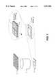
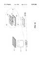
- FIG. 1illustrates a perspective view of a conventional imaging device 2 that includes an IR blocking filter 4, a lens assembly 5, and an imager and package 6.
- the imager and package 6includes a pixel array 7 having a substrate with an active area 8 and a color filter array 9 disposed thereon.
- a CFA element 9is overlaid on the substrate 8 and covers the light sensing circuit.
- the combination of the sensor with the corresponding CFA elementis often referred to as a pixel.
- a red CFA elementis overlaid over a light sensing circuit
- that pixelis referred to as a red pixel
- a green CFA elementis overlaid on a light sensing circuit
- that pixelis referred to as a green pixel.
- imagersThere are two primary types of imagers. First, there are those imagers employing CCD (charge coupled device) technology. Second, there are imagers that are made using complementary metal oxide semiconductor (CMOS) processes.
- CCDcharge coupled device
- CMOScomplementary metal oxide semiconductor
- the responsivity of a pixel of a first coloris different than the responsivity for a pixel of a second color.
- the signal to noise (S/N) ratio of the pixelswill not be equal due to differing responsivity between the pixels.
- Blue pixelstypically have the least responsivity; consequently, the signal to noise ratio of the blue pixels is less than the signal to noise ratio of the red and green pixels.
- the pixels having the greatest sensitivitytypically the red and green pixels
- the storage capacitors associated with the red and green pixelsreach a maximum capacity of stored photoelectrons (i.e., saturate) before the blue pixels.
- Prior art sensorsdo not compensate for color responsivity variation among the different color pixels. Accordingly, when an exposure is made, the exposure time is adjusted to avoid saturation in the most sensitive pixels. Thus, as a result, blooming is avoided in neighboring pixels. The result of this adjustment in exposure time is a degraded signal to noise (S/N) ratio in the least sensitive pixels (typically the blue pixels).
- S/Nsignal to noise
- a conventional approachis to increase the signal to noise ratio of the blue pixels by increasing the integration time (i.e., the exposure time).
- the integration timei.e., the exposure time
- the red and green pixelssaturate and are subject to undesirable saturation artifacts (these undesirable artifacts are commonly referred to in the art as blooming).
- the prior artemployed anti-blooming mechanisms in the pixels.
- these mechanismsincrease the cost and complexity of the color pixels.
- these anti-blooming mechanismsare ineffective to eliminate the blooming effect while still obtaining a desired increase in the signal to noise ratio of the blue pixels.
- a method and apparatus for employing a light shield to modulate pixel color responsivityincludes a substrate having a photodiode with a light receiving area.
- a color filter array material of a first coloris disposed above the substrate.
- the pixelhas a first relative responsivity.
- a light shieldis disposed above the substrate to modulate the pixel color responsivity.
- the light shieldforms an aperture whose area is substantially equal to the light receiving area adjusted by a reduction factor.
- the reduction factoris the result of an arithmetic operation between the first relative responsivity and a second relative responsivity, associated with a second pixel of a second color.
- FIG. 1illustrates an exploded perspective view of a conventional imaging device.
- FIG. 2illustrates an exploded perspective view of a pixel cell configured in accordance to the teachings of one embodiment of the present invention.
- FIG. 3illustrates an exploded perspective view of the pixel cell configured in accordance to the teachings of an alternative embodiment of the present invention.
- FIG. 4is a flowchart illustrating a method of determining the area of openings in a metal mask that is used to pattern a metal layer above each color pixel cell in accordance with one embodiment of the present invention.
- FIG. 5is a flowchart illustrating a method of determining relative responsivity of the color pixels in accordance with one embodiment of the present invention.
- FIG. 6illustrates a top view of the improved pixel cell before a metal shield layer is deposited thereon.
- FIG. 7illustrates a top view of the improved pixel cell of the present invention after a metal shield layer is deposited thereon.
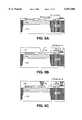
- FIGS. 8A-8Dillustrate a cross-sectional view through A--A of the improved pixel cell of the present invention, where the first metal layer is employed as a light shield.
- FIG. 8Aillustrates a cross-sectional of the improved pixel cell of the present invention after fabrication of active devices by conventional processing methods.
- FIG. 8Billustrates a cross-sectional of the improved pixel cell of the present invention after a first dielectric layer is deposited on the substrate and via lithography and etch have been performed.
- FIG. 8Cillustrates a cross-sectional view of an improved pixel cell of the present invention after deposition of a metal in the vias and a metal polish.
- FIG. 8Dillustrates a cross-sectional view of the improved pixel cell of the present invention where a first metal layer is used as a metal shield to modify the color responsivity of the pixel.
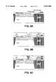
- FIGS. 9A-9Lillustrate a cross-sectional view through A--A of the improved pixel cell of the present invention, where the fourth metal layer is employed as a light shield.
- FIGS. 9A-9Ccorrespond to FIGS. 8A-8C and the structures shown therein are made with the same processing steps, described in FIGS. 8A-8C.
- FIG. 9Dillustrates a cross-sectional view of the improved pixel cell of the present invention after a metal one layer has been deposited, and the metal one layer lithography and etch processing steps have been performed.
- FIG. 9Eillustrates a cross-sectional view of the improved pixel cell of the present invention after 1) a second dieletric layer (IDL1) has been deposited and polished; 2) a via one lithography and etch processing steps have been performed; and 3) a CVD metal deposition and polish have been performed.
- IDL1second dieletric layer
- FIG. 9Fillustrates a cross-sectional view of the improved pixel cell of the present invention after a metal two layer has been deposited, and metal two lithography and etch have been accomplished.
- FIG. 9Gillustrates a cross-sectional view of the improved pixel cell of the present invention after a third dielectric layer has been deposited and polished; via two lithography and etch steps have been performed (although not shown in this cross-sectional view); and a metal deposition and polish have been performed (although not shown in this cross-sectional view).
- FIG. 9Hillustrates a cross-sectional view of the improved pixel cell of the present invention after a metal three layer has been deposited, and the metal three lithography and etch processing steps have been performed.
- FIG. 9Iillustrates a cross-sectional view of the improved pixel cell of the present invention after a fourth dielectric layer has been deposited and polished; a via three lithography and etch processing steps have been performed (although not shown in this cross-sectional view); and a metal deposition and polish have been performed (although not shown in this cross-sectional view).
- FIG. 9Jillustrates a cross-sectional view of the improved pixel cell of the present invention where the fourth metal layer is employed as a light shield to modify the color responsivity of the pixel.
- FIG. 9Kis a cross-sectional view of the improved pixel cell of the present invention after a dielectric is deposited on the fourth metal layer.
- FIG. 9Lillustrates a cross-sectional view of the improved pixel cell of the present invention after color filter array material has been spun onto the dielectric material, and the CFA lithography processing steps of exposure, development, and bake have been performed.
- FIGS. 10A-10Cillustrate a cross-sectional view through B--B of the improved pixel cell of the present invention where the first metal layer is employed as a light shield.
- FIGS. 11A-11Killustrate the cross-sectional views through B--B of the improved pixel cell employing the metal four layer as a light shield.
- FIG. 12illustrates a perspective view of an image capture system in which the improved sensor of the present invention can be implemented.
- FIG. 13illustrates a relative response versus wavelength graph.
- each block within the flowchartsrepresents both a method step and an apparatus element for performing the method step.
- the corresponding apparatus elementmay be configured in hardware, software, firmware or combinations thereof.
- a method and apparatus to compensate the color pixels for color responsivity variation so that the signal to noise ratio for the different color pixels are approximately equal while preventing saturation of pixels of any one colorare disclosed.
- the method and apparatus for employing a light shield to modulate color pixel responsivityhas numerous applications in the imaging field.
- the present inventioncan be advantageously employed to increase the signal to noise ratio of the less sensitive color pixels while preventing the saturation of the more sensitive color pixels. Since the more sensitive color pixels do not saturate, blooming and blooming artifacts are minimized.
- the presently preferred embodimentemploys a metal layer as the light shield, any opaque material that substantially blocks light can be used as a light shield to modulate the color pixel responsivity.
- the aperturehas a generally rectangular shape, apertures having other geometric shapes including, but not limited to, circular pattern, square pattern, can be employed.
- the aperturecan be symmetric or non-symmetric, a single aperture or multiple apertures. The important consideration is that a portion of the light receiving area, as determined by the color responsivity of the pixel and the color responsivity of a second color pixel, is achieved.
- the teachings of the present inventioncan be implemented in image capture systems having fewer or more than three colors and other CFA patterns.
- a four color scheme that employs cyan, white, green and yellowcan be used.
- the cyan, white, green and yellow color schemeplease refer to the article entitled "MOS Solid-State Imager", by Akiya Izumi and Kohichi Mayama, Hitachi Review, Vol. 32, No. 3, pp. 125-128 (1983).
- the present inventioncan be applied to image capture systems having different CFA patterns, such as a cyan, magenta, yellow CFA pattern.
- pixel cellrefers to a light sensing circuit and a color filter array (CFA) material overlaid on top of a light sensor.
- CFAcolor filter array
- a red pixelrefers to a light sensing circuit with a red CFA material overlaid on the light sensor.
- a blue pixelrefers to a blue CFA material overlaid on the light sensor.
- a light sensorcan include a photodiode and associated circuitry (e.g., transistors) to read out the output of the light sensor.
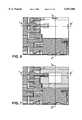
- FIG. 2illustrates an exploded perspective view of an improved pixel cell 200 configured in accordance to the teachings of one embodiment of the present invention.
- the improved pixel cell 200includes a sensor substrate 204 having active devices and a light sensor.
- the light sensorreceives incident light and converts the incident light into an electrical signal representative of said light.
- the light sensorcan be a photoconductor, a photodetector, a phototransistor or photodiode.
- a metal semiconductor photodiodesuch as a PIN structure or a heterojunction photodiode (e.g., GaAs photodiode) can be employed as the light sensor.
- a Schottky diode structurecan also be employed as the sensor.
- a photo-gate structurecan also be used as a light sensor.
- the sensor substrateincludes a photodiode region 208 that is a portion of the pixel cell area 206.
- the photodiode region 208has a predetermined light receiving area which can be the entire photodiode region 208 or a portion thereof.
- the light receiving areacorresponds to the area of an opening 214 in a metal layer, which is described hereinafter.
- the improved cell 200includes at least one metal layer 210 that forms an opening 214.
- the area of this opening 214is important and can be selectively varied for each different color pixel. Determining the area of the opening 214 is described in greater detail hereinafter with reference to FIG. 4.
- the incident illumination 220is incident on the entire pixel cell area 206, because of the conductive metal layer 210, the incident illumination 220 only affects the illuminated area 224. It should be noted that the illuminated area 224 for this pixel cell is a fraction of the entire photodiode region 208.
- the metal one (I) layeris employed as a light shield to affect the color responsivity of the pixel cell.
- FIG. 3illustrates an exploded perspective view of an improved pixel cell 300 configured in accordance to the teachings of an alternative embodiment of the present invention.
- the improved pixel cell 300includes a sensor substrate 304 having active devices and a photodiode.
- the sensor substrate 304includes a photodiode region 308 that is a portion of the pixel cell area 306.
- a conductive metal layer 310forms an opening 314 and acts as a light shield.
- the light shieldis the metal two (II) layer.
- a metal one (I) layer 330, a metal three (III) layer 334, and a metal four (IV) layer(not shown) are employed in this process for local interconnect. It should be noted that any one of the metal layers (metal I, metal II, metal III, metal IV) can be employed as the light shield.
- metal layers that are not employed as the light shieldnot intrude into the photodiode region not covered by the light shield. It is preferable that metal layers above the light shield metal layer be kept as far removed as practical from the opening 314, to minimize any unintended losses due to shadowing or diffractive effects.
- the metal layers below the light shield layerare restricted from intruding into the photodiode region not covered by the light shield. It is not necessary that uniform openings be simultaneously fabricated in all of the metal layers.
- FIG. 4is a flowchart illustrating a method of determining the area of openings in a metal mask for each color pixel cell in accordance with one embodiment of the present invention.
- one of the metal layers(metal I, metal II, metal III or metal IV) is selected to control the pixel cell responsivity.
- processing step 402a determination is made of the relative responsivity of the color pixels. In the example where there are three color pixels (e.g., red pixels, green pixels and blue pixels), a determination is made of the relative responsivities of the R, G, B pixels (i.e., S R , S G , S B are determined).
- decision block 404a determination is made as to which of the color pixels is least sensitive to light.
- processingproceeds to step 410.
- the metal mask employed to form the metal above the red pixelsis configured to have an opening with an area substantially equal to the predetermined light receiving area for all red pixels.
- the metal mask employed to form the metal above the green pixelsis configured to have an opening having an area substantially equal to the predetermined light receiving area adjusted by a reduction factor.
- the reduction factoris the result of an arithmetic operation between S R and S G , and the light receiving area is multiplied by the reduction factor.
- the reduction factorcan be substantially equal to S R /S G .
- the metal mask employed to pattern the metal above the blue pixelsis configured to have an opening having an area substantially equal to the predetermined light receiving area adjusted by a reduction factor.
- the reduction factoris the result of an arithmetic operation between S R and S B , and the light receiving area is multiplied by the reduction factor.
- the reduction factorcan be substantially equal to S R /S B .
- the sensor deviceis fabricated by employing conventional processing techniques.
- the metal mask employed to form the metal above green pixelsis configured to have an opening having an area substantially equal to the predetermined light receiving area.
- the metal mask employed to form the metal above blue pixelsis configured to have an opening having an area substantially equal to the predetermined light receiving area adjusted by a reduction factor.
- the reduction factoris the result of an arithmetic operation between S G and S B , and the light receiving area is multiplied by the reduction factor.
- the reduction factorcan be substantially equal to S G /S B .
- the metal mask employed to pattern the metal above red pixelsis configured to have an opening having an area substantially equal to the predetermined light receiving area adjusted by a reduction factor.
- the reduction factoris the result of an arithmetic operation between S G and S R , and the light receiving area is multiplied by the reduction factor.
- the reduction factorcan be substantially equal to S G /S R . Processing then proceeds to processing step 414.
- the metal mask employed to pattern the metal above blue pixelsis configured to have an opening having an area substantially equal to the predetermined light receiving area.
- the metal mask employed to pattern the metal above the red pixelsis configured to have an opening having an area substantially equal to the predetermined light receiving area adjusted by a reduction factor.
- the reduction factoris the result of an arithmetic operation between S B and S R , and the light receiving area is multiplied by the reduction factor.
- the reduction factorcan be substantially equal to S B /S R .
- the metal mask employed to pattern the metal above green pixelsincludes an opening having an area substantially equal to the predetermined light receiving area adjusted by a reduction factor.
- the reduction factoris the result of an arithmetic operation between S B and S G , and the light receiving area is multiplied by the reduction factor.
- the reduction factorcan be substantially equal to S B /S G .
- FIG. 5is a flowchart illustrating the method steps for determining pixel responsivity in accordance with the teachings of the present invention.
- the input photodiode responsivity(Resp( ⁇ )) is determined.
- input color filter array transmittance for each color T R ( ⁇ ), T G ( ⁇ ), T B ( ⁇ )is determined.
- the input IR blocking filter characteristics(IR( ⁇ )) are determined.
- a net spectral responseis computed. The net response is simply the responsivity multiplied by the input color filter array transmittance multiplied by the input IR blocking filter characteristic.
- the input light source spectral characteristicsare determined.
- the input light source spectral characteristicsare conventionally CIE D65 or sunlight.
- the net response, calculated in processing step 506,is convolved with the input light source characteristics, determined in processing step 508, to obtain a relative responsivity for each color (i.e., S R , S G and S B are determined).
- FIG. 6illustrates a top view of the improved pixel cell before a metal shield layer is deposited thereon.
- FIG. 7illustrates a top view of the improved pixel cell of the present invention after a metal shield layer is deposited thereon.
- FIGS. 8A-8Cillustrate a cross-sectional view of the improved pixel cell of the present invention through A--A of FIG. 6, and FIG. 8D illustrates a cross-sectional view of the improved pixel cell of the present invention through A--A of FIG. 7, where the first metal layer is employed as a light shield.
- FIG. 8Aillustrates a cross-sectional of the improved pixel cell of the present invention after fabrication of active devices by conventional processing methods.
- the photodiodeis formed by the N-well and P-region, and the trench oxide provides a transparent opening to receive light.
- FIG. 8Billustrates a cross-sectional of the improved pixel cell of the present invention after a first dielectric layer (herein referred to as an inter-layer dielectric (ILD0)) is deposited on the substrate and via lithography and etch has been performed.
- ILD0inter-layer dielectric
- Via lithographyinvolves coating the dielectric layer with a photoresist material, exposing the photoresist material through a mask, and removing the exposed photoresist in a developing step.
- the via etchinvolves transferring the mask pattern from the photoresist material to the first dielectric layer.
- the etching stepalso involves the removal of the photoresist material.
- Via lithography and etchare well known in the art and employ conventional processing steps and processing equipment.
- FIG. 8Cillustrates a cross-sectional view of an improved pixel cell of the present invention after chemical vapor deposition (CVD) of a metal (e.g., tungsten) in the vias and a metal polish.
- CVDchemical vapor deposition
- FIG. 8Dillustrates a cross-sectional view of the improved pixel cell of the present invention where the first metal layer (M1) is used as a metal shield to modify the color responsivity of the pixel.
- the metal one layeris configured to restrict the amount of incident light on the predetermined light receiving area.
- FIGS. 9A-9Lillustrate a method of manufacturing the improved pixel cell of the present invention where a metal four layer is employed as a light shield.
- FIGS. 9A-9Lare sectional views through A--A of FIG. 6 and FIG. 7.
- FIGS. 9A-9Care identical to FIGS. 8A-8C and the structures shown therein are made with the same processing steps.
- FIG. 9Dillustrates a cross-sectional view of the improved pixel cell of the present invention after a metal one layer has been deposited, and the metal one layer lithography and etch processing steps have been performed.
- FIG. 9Eillustrates a cross-sectional view of the improved pixel cell of the present invention after 1) a second dieletric layer (IDL1) has been deposited and polished; 2) a via one lithography and etch processing steps have been performed; and 3) a CVD metal deposition and polish have been performed.
- IDL1second dieletric layer
- FIG. 9Fillustrates a cross-sectional view of the improved pixel cell of the present invention after a metal two layer has been deposited, and metal two lithography and etch have been accomplished.
- FIG. 9Gillustrates a cross-sectional view of the improved pixel cell of the present invention after 1) a third dielectric layer (IDL2) has been deposited and polished; 2) via two lithography and etch steps are also performed (although not shown in this cross-sectional view); and 3) a CVD deposition and polish of a metal, such as tungsten, is also performed (although not shown in this cross-sectional view).
- IDL2third dielectric layer
- FIG. 9Hillustrates a cross-sectional view of the improved pixel cell of the present invention after a metal three layer has been deposited, and the metal three lithography and etch processing steps have been performed.
- FIG. 9Iillustrates a cross-sectional view of the improved pixel cell of the present invention after 1) a fourth dielectric layer (IDL3) has been deposited and polished; 2) a via three lithography and etch processing steps are also performed (although not shown in this cross-sectional view); and 3) a CVD deposition of metal and corresponding polish is also performed (although not shown in this cross-sectional view).
- IDL3fourth dielectric layer
- FIG. 9Jillustrates a cross-sectional view of the improved pixel cell of the present invention where the fourth metal layer (M4) is employed as a light shield to modify the color responsivity of the pixel.
- M4fourth metal layer
- FIG. 9Kis a cross-sectional view of the improved pixel cell of the present invention after a dielectric, such as silicon nitride, is deposited on the fourth metal layer.
- a dielectricsuch as silicon nitride
- the silicon nitrideis used as passivation to prevent sodium and moisture from attacking the die.
- FIG. 9Lillustrates a cross-sectional view of the improved pixel cell of the present invention after color filter array material has been spun onto the silicon nitride layer, and the CFA lithography processing steps of exposure, and development and CFA bake have been performed.
- the CFA spin code, lithography and bake processis repeated as many times as there are different colors in the color filter array (CFA). For example, if the color filter array employs a red color, green color, and blue color, the CFA processing steps are repeated three times.
- FIGS. 10A-10Cillustrate a cross-sectional view through B--B of the improved pixel cell of the present invention where the first metal layer is employed as a light shield.
- FIGS. 11A-11Killustrate the cross-sectional views through B--B of the improved pixel cell employing the metal four layer as a light shield.
- FIGS. 10A-10C and FIGS. 11A-Kcorrespond generally to the process flow described with reference to FIGS. 8A-8D and 9A-9L, the description of the processing steps are not repeated herein.
- the teachings of the present inventionmodify the design principles for conventional pixel layout. Whereas in conventional pixel layouts, the metal layers are used exclusively for electrical connection, the present invention teaches that one of the metal layers can be used for both interconnect and as an optical element to modulate the color responsivity of pixels. Moreover, whereas conventional layout rules specifically avoid intrusion into the region above the photodiode, the present invention teaches deliberately routing one level of metal to selectively intrude into the region above the photodiode to reduce incident light and modulate the color responsivity of the pixel.
- the metal layers and interconnect above and below the light modulating layercan intrude into the photodiode region to the extent that the light modulating layer covers the predetermined light receiving area. It is important that the other metal layers do not intrude into the non-covered optical path specified by the light shield layer. It is also important to note that the use of a metal layer for light modulation and as a light shield does not preclude that metal layer for use as an interconnect.
- the pixelis manufactured by an Intel proprietary P854 advanced logic process. Salient features of the P854 process are that it employs multiple metal layers (specifically, four metal layers) and that it exhibits a 0.35 micron ( ⁇ m) minimum feature size.
- Salient features of the P854 processare that it employs multiple metal layers (specifically, four metal layers) and that it exhibits a 0.35 micron ( ⁇ m) minimum feature size.
- ⁇ mmicron
- the light shieldis a metal layer because the metal process is superior to the process for other layers when it comes to small features and control of the actual etching process.
- the P854 process advanced logic processcan be employed to control metal line widths of approximately 0.4 to 1.5 microns, depending on the layer number.
- the present inventionemploys a metal layer as a light shield or a light window.
- the present inventionemploys the metal layer as a responsivity modulation device. Since the responsivity of a color pixel is proportional to the light energy (e.g., color of the incident light) and also the intensity of the light incident on an exposed area (e.g., photodiode), the present invention employs metal to affect the exposed area (i.e., the area than can receive the photons of light) to compensate for different incident light energy (different colors of light) so as to achieve a balanced response to the light energy distribution expected for a typical scene.
- the exposed areai.e., the area than can receive the photons of light
- FIG. 12illustrates a perspective view of an image capture system 1200 in which the improved sensor of the present invention can be implemented.
- the image capture system 1200includes an IR blocking filter 1210, a lens assembly 1214 and the imager and package 1218.
- the imagerincludes a sensor circuit 1224.
- the sensor circuitincludes a pixel array 1228 having a plurality of pixel cells arranged in rows and columns.
- the pixel arrayconfigured with the teachings of the present invention, includes a light shield metal layer 1230 having a plurality of openings where the area of the openings is specifically configured based on the color responsivity of the pixel cell.
- the pixel arrayalso includes a color filter array 1232 having a plurality of elements.
- the color filter arrayemploys three color filter materials (red, green and blue).
- the metal layerincludes a plurality of responsivity altering windows, where the windows disposed above the blue pixels are approximately equal to 5 microns by 5 microns, the windows disposed above red and green pixels are approximately 2 microns by 2 micron.
- the openings employed for controlling the pixel responsivitycan range in size from a minimum set by the fabrication process capability to a maximum which results in no blockage of light entering the photodiode (as shown in FIG. 2). It is anticipated that a typical embodiment would require openings ranging from approximately one micron by one micron to 5 microns by 5 microns.
- a photosensitive deviceincludes a first area for receiving incident light.
- the photosensitive devicehas a responsivity with respect to the wavelength of the incident light.
- the responsivity of the photosensitive deviceis dependent on the wavelength of the incident light.
- the present inventionemploys metal to selectively affect the responsivity of the photosensitive device by covering a portion of the area of photodiode.
- the exposed area of the red pixels, the green pixels and the blue pixelsare selectively adjusted so that all of the pixels, regardless of color, saturate at approximately the same time in response to the light energy distribution expected for a typical scene.
- the present inventionallows all the color pixels to be exposed to the light (i.e., control the exposure or integration time) so that all the color pixels saturate at about the same time.
- the graph corresponding to step 500 in FIG. 5is a responsivity versus wavelength curve for an unfiltered pixel (i.e., that is a pixel without any color filter array material disposed thereon).
- the responsivityis related to the quantum efficiency of the photodiode.
- the quantum efficiency(sometimes referred to as effective quantum efficiency) is often expressed as a ratio of the number of photoelectrons created by the photoelectric effect to the number of photons incident on the entire pixel area even though the active area (the predetermined light receiving area) is typically less than the entire pixel area.
- the wavelengthrefers to the wavelength of the incident light.
- the graph corresponding to step 502 of FIG. 5illustrates a transmittance versus wavelength curve for different color filter materials.
- the sensor responsivity versus wavelength curvequantum efficiency versus wavelength
- a net responsivity versus wavelength curve(see graph associated with step 506) that models the behavior of a color pixel is determined.
- a fill factor percentage of 31%represents an exposure of the entire active area.
- the horizontal axisis the transmittance, which is the fraction of the incident light that reaches the active area.
- the transmittancemay be expressed as a percentage, or as a fraction between 0 and 1.
- the term, "transmissivity”,may be loosely applied by those skilled in the art, although a strict definition of transmissivity is the fraction of light passing through a material per unit thickness. Thus, transmissivity is an intrinsic material property, while transmittance is an extrinsic material property.
- FIG. 13is a relative response versus wavelength graph illustrating five curves with each curve corresponding to a fill factor (FF) percentage.
- the fill factoris the percentage of the total pixel area which is open to incident light.
- a pixelcan be divided into an active area (i.e., the area having the circuit element to convert light photons into electrons) and areas where other circuits are located.
- the fill factor percentagerefers to the amount of active area that is uncovered divided by the total pixel area. For example, in this example, an uncovered pixel (i.e., 100% of the total pixel area is exposed to light), the fill factor percentage is approximately 31%.
- the fill factor percentagesare approximately 6.2%, only a small fraction of the light is detected.
- the amount of light detected by the active areacorrespondingly decreases.
- the second source of noiseis dark current.
- Dark currentrepresents a leakage current that causes the accumulation of stored electrons over the integration period.
- the electrons contributed from the dark currentcannot be distinguished from photoelectrons, and hence are undesirable.
- the dark current contribution to the signalis smaller than the shot noise.
- increasing the number of photoelectrons captured in the least sensitive pixelsbenefits the signal to noise ratio.
- the present inventionallows a longer exposure for the benefit of the least sensitive pixels without saturation of the more sensitive color pixels thereby decreasing the shot noise in the image capture system.
Landscapes
- Solid State Image Pick-Up Elements (AREA)
- Spectrometry And Color Measurement (AREA)
- Optical Elements Other Than Lenses (AREA)
- Studio Devices (AREA)
Abstract
Description
Claims (9)
Priority Applications (8)
| Application Number | Priority Date | Filing Date | Title |
|---|---|---|---|
| US08/937,631US6057586A (en) | 1997-09-26 | 1997-09-26 | Method and apparatus for employing a light shield to modulate pixel color responsivity |
| PCT/US1998/014521WO1999017337A1 (en) | 1997-09-26 | 1998-07-13 | Method and apparatus for employing a light shield to modulate pixel color responsivity |
| KR1020007003246AKR100358862B1 (en) | 1997-09-26 | 1998-07-13 | Method and apparatus for employing a light shield to modulate pixel color responsivity |
| EP98934508AEP1018141A4 (en) | 1997-09-26 | 1998-07-13 | Method and apparatus for employing a light shield to modulate pixel color responsivity |
| AU84015/98AAU8401598A (en) | 1997-09-26 | 1998-07-13 | Method and apparatus for employing a light shield to modulate pixel color responsivity |
| JP2000514306AJP2001518703A (en) | 1997-09-26 | 1998-07-13 | Method and apparatus for using light-blocking layer to change pixel color responsivity |
| US09/524,081US6235549B1 (en) | 1997-09-26 | 2000-03-13 | Method and apparatus for employing a light shield to modulate pixel color responsivity |
| US09/802,464US6933168B2 (en) | 1997-09-26 | 2001-03-09 | Method and apparatus for employing a light shield to modulate pixel color responsivity |
Applications Claiming Priority (1)
| Application Number | Priority Date | Filing Date | Title |
|---|---|---|---|
| US08/937,631US6057586A (en) | 1997-09-26 | 1997-09-26 | Method and apparatus for employing a light shield to modulate pixel color responsivity |
Related Child Applications (1)
| Application Number | Title | Priority Date | Filing Date |
|---|---|---|---|
| US09/524,081DivisionUS6235549B1 (en) | 1997-09-26 | 2000-03-13 | Method and apparatus for employing a light shield to modulate pixel color responsivity |
Publications (1)
| Publication Number | Publication Date |
|---|---|
| US6057586Atrue US6057586A (en) | 2000-05-02 |
Family
ID=25470186
Family Applications (3)
| Application Number | Title | Priority Date | Filing Date |
|---|---|---|---|
| US08/937,631Expired - LifetimeUS6057586A (en) | 1997-09-26 | 1997-09-26 | Method and apparatus for employing a light shield to modulate pixel color responsivity |
| US09/524,081Expired - LifetimeUS6235549B1 (en) | 1997-09-26 | 2000-03-13 | Method and apparatus for employing a light shield to modulate pixel color responsivity |
| US09/802,464Expired - LifetimeUS6933168B2 (en) | 1997-09-26 | 2001-03-09 | Method and apparatus for employing a light shield to modulate pixel color responsivity |
Family Applications After (2)
| Application Number | Title | Priority Date | Filing Date |
|---|---|---|---|
| US09/524,081Expired - LifetimeUS6235549B1 (en) | 1997-09-26 | 2000-03-13 | Method and apparatus for employing a light shield to modulate pixel color responsivity |
| US09/802,464Expired - LifetimeUS6933168B2 (en) | 1997-09-26 | 2001-03-09 | Method and apparatus for employing a light shield to modulate pixel color responsivity |
Country Status (6)
| Country | Link |
|---|---|
| US (3) | US6057586A (en) |
| EP (1) | EP1018141A4 (en) |
| JP (1) | JP2001518703A (en) |
| KR (1) | KR100358862B1 (en) |
| AU (1) | AU8401598A (en) |
| WO (1) | WO1999017337A1 (en) |
Cited By (33)
| Publication number | Priority date | Publication date | Assignee | Title |
|---|---|---|---|---|
| US6278169B1 (en)* | 1998-05-07 | 2001-08-21 | Analog Devices, Inc. | Image sensor shielding |
| US6507083B1 (en) | 2000-10-05 | 2003-01-14 | Pixim, Inc. | Image sensor with light-reflecting via structures |
| US6512401B2 (en) | 1999-09-10 | 2003-01-28 | Intel Corporation | Output buffer for high and low voltage bus |
| WO2003025838A1 (en)* | 2001-09-14 | 2003-03-27 | The Arizona Board Of Regents On Behalf Of The University Of Arizona | Inter-objective baffle system |
| US6559914B1 (en) | 2001-07-05 | 2003-05-06 | International Rectifier Corp. | Conductive black matrix layer for LCD display connected to gate through two vias |
| US20030103150A1 (en)* | 2001-11-30 | 2003-06-05 | Catrysse Peter B. | Integrated color pixel ( ICP ) |
| US20040101210A1 (en)* | 2001-03-19 | 2004-05-27 | The Arizona Board Of Regents On Behalf Of The University Of Arizona | Miniaturized microscope array digital slide scanner |
| US6825470B1 (en)* | 1998-03-13 | 2004-11-30 | Intel Corporation | Infrared correction system |
| EP1475963A3 (en)* | 2003-04-07 | 2005-02-02 | Matsushita Electric Industrial Co., Ltd. | Solid-state imaging device, signal processing device, camera and spectral device |
| US20050052561A1 (en)* | 2003-09-04 | 2005-03-10 | Altice Peter P. | Metal mask for light intensity determination and adc calibration |
| US20050062863A1 (en)* | 2003-09-19 | 2005-03-24 | Fuji Photo Film Co., Ltd. | Solid state imaging device |
| US6943424B1 (en)* | 2004-05-06 | 2005-09-13 | Optopac, Inc. | Electronic package having a patterned layer on backside of its substrate, and the fabrication thereof |
| US20060011808A1 (en)* | 2004-07-19 | 2006-01-19 | Jiutao Li | CMOS front end process compatible low stress light shield |
| US20060104564A1 (en)* | 2004-11-15 | 2006-05-18 | Catrysse Peter B | Integrated waveguide and method for designing integrated waveguide |
| US20060249653A1 (en)* | 2005-05-06 | 2006-11-09 | Gazeley William G | Pixel with spatially varying metal route positions |
| US20060249654A1 (en)* | 2005-05-06 | 2006-11-09 | Silsby Christopher D | Pixel with spatially varying sensor positions |
| US20070023799A1 (en)* | 2005-08-01 | 2007-02-01 | Micro Technology, Inc. | Structure and method for building a light tunnel for use with imaging devices |
| US20070030366A1 (en)* | 2005-07-20 | 2007-02-08 | Eastman Kodak Company | Selective pixel binning and averaging based on scene illuminant |
| US20070188635A1 (en)* | 2006-02-15 | 2007-08-16 | Takumi Yamaguchi | Solid-state imaging device and camera |
| US20090200451A1 (en)* | 2008-02-08 | 2009-08-13 | Micron Technology, Inc. | Color pixel arrays having common color filters for multiple adjacent pixels for use in cmos imagers |
| US20090302323A1 (en)* | 2008-06-04 | 2009-12-10 | Micron Technology, Inc. | Method and apparatus for providing a low-level interconnect section in an imager device |
| US20110216229A1 (en)* | 2008-09-11 | 2011-09-08 | Alexandre Mary | Nanostructured spectral filter and image sensor |
| US20120007203A1 (en)* | 2010-07-07 | 2012-01-12 | Canon Kabushiki Kaisha | Solid-state imaging apparatus and imaging system |
| US8687246B2 (en) | 2010-07-07 | 2014-04-01 | Canon Kabushiki Kaisha | Solid-state imaging apparatus and imaging system |
| US8742359B2 (en) | 2010-07-07 | 2014-06-03 | Canon Kabushiki Kaisha | Solid-state imaging apparatus and imaging system |
| US8836833B2 (en) | 2010-07-07 | 2014-09-16 | Canon Kabushiki Kaisha | Solid-state imaging apparatus having pixels with plural semiconductor regions |
| US20140374574A1 (en)* | 2013-06-20 | 2014-12-25 | Stmicroelectronics (Crolles 2) Sas | Forming of a nanostructured spectral filter |
| US9007501B2 (en) | 2010-07-07 | 2015-04-14 | Canon Kabushiki Kaisha | Solid-state imaging apparatus and imaging system |
| US20210203830A1 (en)* | 2018-08-20 | 2021-07-01 | Facebook Technologies, Llc | Pixel sensor having adaptive exposure time |
| US11863886B2 (en) | 2018-06-27 | 2024-01-02 | Meta Platforms Technologies, Llc | Pixel sensor having multiple photodiodes |
| US11877080B2 (en) | 2019-03-26 | 2024-01-16 | Meta Platforms Technologies, Llc | Pixel sensor having shared readout structure |
| US11910114B2 (en) | 2020-07-17 | 2024-02-20 | Meta Platforms Technologies, Llc | Multi-mode image sensor |
| US11956413B2 (en) | 2018-08-27 | 2024-04-09 | Meta Platforms Technologies, Llc | Pixel sensor having multiple photodiodes and shared comparator |
Families Citing this family (49)
| Publication number | Priority date | Publication date | Assignee | Title |
|---|---|---|---|---|
| EP2290952A3 (en)* | 2000-07-27 | 2011-08-17 | Canon Kabushiki Kaisha | Image sensing apparatus |
| US6958777B1 (en)* | 2000-09-29 | 2005-10-25 | Ess Technology, Inc. | Exposure control in electromechanical imaging devices |
| US6806569B2 (en)* | 2001-09-28 | 2004-10-19 | Intel Corporation | Multi-frequency power delivery system |
| US20050285956A1 (en)* | 2001-11-15 | 2005-12-29 | Stmicroelectronics N.V. | Color-filter array for an optical-image sensor |
| DE50212030D1 (en)* | 2001-11-15 | 2008-05-15 | St Microelectronics Nv | COLOR FILTER MATRIX FOR AN OPTICAL IMAGE SENSOR |
| US7034957B2 (en)* | 2002-04-15 | 2006-04-25 | Shang-Yu Yang | Method for increasing signal to noise ratio |
| JP2004104203A (en)* | 2002-09-05 | 2004-04-02 | Toshiba Corp | Solid-state imaging device |
| US7453129B2 (en) | 2002-12-18 | 2008-11-18 | Noble Peak Vision Corp. | Image sensor comprising isolated germanium photodetectors integrated with a silicon substrate and silicon circuitry |
| US7012314B2 (en)* | 2002-12-18 | 2006-03-14 | Agere Systems Inc. | Semiconductor devices with reduced active region defects and unique contacting schemes |
| EP1746638A3 (en)* | 2002-12-18 | 2011-03-23 | Noble Peak Vision Corp. | Semiconductor devices with reduced active region defectcs and unique contacting schemes |
| US6812539B1 (en)* | 2003-04-10 | 2004-11-02 | Micron Technology, Inc. | Imager light shield |
| JP4824542B2 (en)* | 2003-05-08 | 2011-11-30 | ザ サイエンス アンド テクノロジー ファシリティーズ カウンシル | electronic microscope |
| US6852562B1 (en)* | 2003-12-05 | 2005-02-08 | Eastman Kodak Company | Low-cost method of forming a color imager |
| EP1594321A3 (en)* | 2004-05-07 | 2006-01-25 | Dialog Semiconductor GmbH | Extended dynamic range in color imagers |
| KR100614793B1 (en)* | 2004-09-23 | 2006-08-22 | 삼성전자주식회사 | Image Sensors and Methods of Manufacturing the Same. |
| SE0402576D0 (en)* | 2004-10-25 | 2004-10-25 | Forskarpatent I Uppsala Ab | Multispectral and hyperspectral imaging |
| US7420680B2 (en)* | 2004-11-16 | 2008-09-02 | Datacolor Holding Ag | Method for designing a colorimeter having integral CIE color-matching filters |
| WO2006055682A2 (en)* | 2004-11-17 | 2006-05-26 | Datacolor Holding Ag | Tristimulus colorimeter having integral dye filters |
| US7580130B2 (en)* | 2005-03-23 | 2009-08-25 | Datacolor Holding Ag | Method for designing a colorimeter having integral illuminant-weighted CIE color-matching filters |
| US7474402B2 (en)* | 2005-03-23 | 2009-01-06 | Datacolor Holding Ag | Reflectance sensor for integral illuminant-weighted CIE color matching filters |
| US7534982B2 (en)* | 2005-06-09 | 2009-05-19 | Micron Technology, Inc. | Reduced imager crosstalk and pixel noise using extended buried contacts |
| US7684794B1 (en)* | 2005-07-01 | 2010-03-23 | Cisco Technologies, Inc. | Managing endpoint addresses separately from managing endpoint mobility |
| US7633106B2 (en)* | 2005-11-09 | 2009-12-15 | International Business Machines Corporation | Light shield for CMOS imager |
| KR100746458B1 (en)* | 2006-10-11 | 2007-08-03 | 매그나칩 반도체 유한회사 | Stacked Pixels for High Resolution CMOS Image Sensors |
| KR100881200B1 (en)* | 2007-07-30 | 2009-02-05 | 삼성전자주식회사 | CMOS image sensor and its manufacturing method |
| KR101411301B1 (en)* | 2007-08-24 | 2014-06-25 | 삼성전자주식회사 | Method for stabilizing black level of image sensor and image sensor |
| US7675024B2 (en)* | 2008-04-23 | 2010-03-09 | Aptina Imaging Corporation | Method and apparatus providing color filter array with non-uniform color filter sizes |
| US20090294244A1 (en)* | 2008-05-30 | 2009-12-03 | Harold Charych | Currency Validator with Rejected Bill Image Storage |
| DE102008027188A1 (en)* | 2008-06-06 | 2009-12-10 | Volkswagen Ag | Image acquisition unit for detecting e.g. color information, has light sensors that act as intensity and color sensors, where number of intensity sensors is greater than number of color sensors |
| KR101024728B1 (en)* | 2008-09-30 | 2011-03-24 | 주식회사 동부하이텍 | Image sensor and manufacturing method |
| US20100208266A1 (en)* | 2009-02-17 | 2010-08-19 | Colman Shannon | Tristimulus colorimeter having integral dye filters |
| US9142586B2 (en) | 2009-02-24 | 2015-09-22 | Taiwan Semiconductor Manufacturing Company, Ltd. | Pad design for backside illuminated image sensor |
| US8531565B2 (en) | 2009-02-24 | 2013-09-10 | Taiwan Semiconductor Manufacturing Company, Ltd. | Front side implanted guard ring structure for backside illuminated image sensor |
| US8264377B2 (en) | 2009-03-02 | 2012-09-11 | Griffith Gregory M | Aircraft collision avoidance system |
| JP5476745B2 (en)* | 2009-03-05 | 2014-04-23 | ソニー株式会社 | SOLID-STATE IMAGING DEVICE, ITS MANUFACTURING METHOD, AND ELECTRONIC DEVICE |
| JP2011138942A (en)* | 2009-12-28 | 2011-07-14 | Oki Semiconductor Co Ltd | Semiconductor element and method of fabricating semiconductor element |
| EP2933629B1 (en) | 2010-02-19 | 2019-04-10 | Pacific Biosciences Of California, Inc. | System for measuring analytical reactions comprising a socket for an optode array chip |
| GB201020024D0 (en)* | 2010-11-25 | 2011-01-12 | St Microelectronics Ltd | Radiation sensor |
| WO2012069851A1 (en)* | 2010-11-25 | 2012-05-31 | Stmicroelectronics (Research & Development) Limited | Radiation sensor |
| GB201020023D0 (en) | 2010-11-25 | 2011-01-12 | St Microelectronics Ltd | Radiation sensor |
| GB2485996A (en) | 2010-11-30 | 2012-06-06 | St Microelectronics Res & Dev | A combined proximity and ambient light sensor |
| GB2486000A (en) | 2010-11-30 | 2012-06-06 | St Microelectronics Res & Dev | Optical proximity detectors with arrangements for reducing internal light propagation from emitter to detector |
| GB2485998A (en) | 2010-11-30 | 2012-06-06 | St Microelectronics Res & Dev | A single-package optical proximity detector with an internal light baffle |
| WO2016098912A1 (en)* | 2014-12-15 | 2016-06-23 | 재단법인 다차원 스마트 아이티 융합시스템 연구단 | Sensor array for multi-aperture camera, and operation method therefor |
| TWI565323B (en)* | 2015-09-02 | 2017-01-01 | 原相科技股份有限公司 | Imaging device for distinguishing foreground and operation method thereof, and image sensor |
| CN109426766A (en)* | 2017-08-23 | 2019-03-05 | 上海箩箕技术有限公司 | Fingerprint imaging mould group and electronic equipment |
| WO2019164898A1 (en) | 2018-02-20 | 2019-08-29 | Intelligent Cleaning Equipment Holdings Co. Ltd. | Tracking device, system for tracking objects, and associated method of use |
| US11172142B2 (en)* | 2018-09-25 | 2021-11-09 | Taiwan Semiconductor Manufacturing Co., Ltd. | Image sensor for sensing LED light with reduced flickering |
| US11682313B2 (en) | 2021-03-17 | 2023-06-20 | Gregory M. Griffith | Sensor assembly for use in association with aircraft collision avoidance system and method of using the same |
Citations (9)
| Publication number | Priority date | Publication date | Assignee | Title |
|---|---|---|---|---|
| US3832034A (en)* | 1973-04-06 | 1974-08-27 | Ibm | Liquid crystal display assembly |
| US4908518A (en)* | 1989-02-10 | 1990-03-13 | Eastman Kodak Company | Interline transfer CCD image sensing device with electrode structure for each pixel |
| JPH06151797A (en)* | 1992-11-11 | 1994-05-31 | Sony Corp | Solid-state image sensor |
| US5352920A (en)* | 1988-06-06 | 1994-10-04 | Canon Kabushiki Kaisha | Photoelectric converter with light shielding sections |
| US5455415A (en)* | 1992-08-25 | 1995-10-03 | Nippondenso Co., Ltd. | Insolation sensor |
| US5471515A (en)* | 1994-01-28 | 1995-11-28 | California Institute Of Technology | Active pixel sensor with intra-pixel charge transfer |
| US5506430A (en)* | 1992-03-03 | 1996-04-09 | Canon Kabushiki Kaisha | Solid state image pick-up device with differing capacitances |
| US5537232A (en)* | 1993-10-05 | 1996-07-16 | In Focus Systems, Inc. | Reflection hologram multiple-color filter array formed by sequential exposure to a light source |
| US5552630A (en)* | 1990-04-13 | 1996-09-03 | Fuji Xerox Co., Ltd. | Thin film transistor having metallic light shield |
Family Cites Families (38)
| Publication number | Priority date | Publication date | Assignee | Title |
|---|---|---|---|---|
| US3963925A (en)* | 1975-02-26 | 1976-06-15 | Texas Instruments Incorporated | Photoconductive detector and method of fabrication |
| JPS5689176A (en)* | 1979-12-20 | 1981-07-20 | Matsushita Electric Ind Co Ltd | Solid image pickup device |
| US4355456A (en)* | 1980-03-07 | 1982-10-26 | General Dynamics, Pomona Division | Process of fabricating a Schottky barrier photovoltaic detector |
| US4789888A (en)* | 1980-04-02 | 1988-12-06 | Matsushita Electric Industrial Co., Ltd. | Solid-state image sensor |
| DE3120849A1 (en)* | 1981-05-26 | 1982-12-23 | Agfa-Gevaert Ag, 5090 Leverkusen | COLOR FILTER ARRANGEMENT FOR AN OPTOELECTRONIC CONVERTER DEVICE |
| DE3686184T2 (en)* | 1985-03-21 | 1993-02-25 | Abbott Lab | SPECTRAL PHOTOMETER. |
| JPS6242449A (en)* | 1985-08-19 | 1987-02-24 | Toshiba Corp | Color solid-state imaging device |
| US4870483A (en)* | 1985-10-02 | 1989-09-26 | Canon Kabushiki Kaisha | Color image sensor including a plurality of photocells and a plurality of colored filters provided on the plurality of photocells |
| JPS62289087A (en)* | 1986-06-09 | 1987-12-15 | Seiko Epson Corp | Solid-state image pickup element |
| JPS6434050A (en)* | 1987-07-29 | 1989-02-03 | Canon Kk | Line sensor for reading color |
| JPS6467960A (en)* | 1987-09-09 | 1989-03-14 | Toshiba Corp | Color solid-state image sensing element |
| US4882490A (en)* | 1987-09-22 | 1989-11-21 | Fuji Photo Film Co., Ltd. | Light beam scanning apparatus having two detectors whose signal ratio indicates main scanning position |
| US4985760A (en)* | 1987-10-09 | 1991-01-15 | Canon Kabushiki Kaisha | Color imager having varying filter aperture sizes to compensate for luminance differences between colors |
| JPH01152663A (en)* | 1987-12-09 | 1989-06-15 | Oki Electric Ind Co Ltd | Solid-state image sensor |
| GB8927915D0 (en)* | 1989-12-11 | 1990-02-14 | Hoffmann La Roche | Novel alcohols |
| US5119181A (en)* | 1990-03-30 | 1992-06-02 | Xerox Corporation | Color array for use in fabricating full width arrays |
| JPH04334056A (en)* | 1991-05-09 | 1992-11-20 | Toshiba Corp | Manufacturing method of solid-state imaging device |
| JPH05183141A (en)* | 1991-07-12 | 1993-07-23 | Fuji Xerox Co Ltd | Color image sensor |
| EP0576144B1 (en)* | 1992-05-22 | 1998-08-05 | Matsushita Electronics Corporation | Solid state image sensor and manufacturing method thereof |
| DE69323618T3 (en)* | 1992-11-06 | 2005-02-03 | Denso Corp., Kariya | PYRHELIOMETRIC SENSOR |
| JPH06224403A (en)* | 1993-01-26 | 1994-08-12 | Matsushita Electron Corp | Solid-state image pickup device and its manufacture |
| DE4329838B4 (en)* | 1993-09-03 | 2005-09-22 | Hynix Semiconductor Inc., Ichon | Solid-state image sensor |
| JP3303482B2 (en)* | 1993-12-07 | 2002-07-22 | 株式会社デンソー | Optical position detector |
| KR0136933B1 (en)* | 1994-05-21 | 1998-04-24 | 문정환 | CDD image device and manufacturing method |
| JP2571018B2 (en)* | 1994-05-31 | 1997-01-16 | 日本電気株式会社 | Method for manufacturing solid-state imaging device |
| JPH08271880A (en)* | 1995-04-03 | 1996-10-18 | Toshiba Corp | Light-shielding film, liquid crystal display device, and material for forming light-shielding film |
| JP3405620B2 (en)* | 1995-05-22 | 2003-05-12 | 松下電器産業株式会社 | Solid-state imaging device |
| US5719075A (en)* | 1995-07-31 | 1998-02-17 | Eastman Kodak Company | Method of making a planar charge coupled device with edge aligned implants and electrodes connected with overlying metal |
| JPH0992809A (en)* | 1995-09-27 | 1997-04-04 | Nikon Corp | Solid-state imaging device |
| US5708264A (en)* | 1995-11-07 | 1998-01-13 | Eastman Kodak Company | Planar color filter array for CCDs from dyed and mordant layers |
| US5986297A (en)* | 1996-05-22 | 1999-11-16 | Eastman Kodak Company | Color active pixel sensor with electronic shuttering, anti-blooming and low cross-talk |
| KR100215878B1 (en)* | 1996-12-28 | 1999-08-16 | 구본준 | Method for manufacturing color solid state image pick-up device |
| JP3547280B2 (en)* | 1997-02-25 | 2004-07-28 | 松下電器産業株式会社 | Solid-state imaging device |
| KR100223805B1 (en)* | 1997-06-13 | 1999-10-15 | 구본준 | Method of manufacturing ccd |
| TW377517B (en)* | 1998-03-19 | 1999-12-21 | United Microelectronics Corp | Color sensing apparatus of diode and the method of manufacturing the same |
| US5914749A (en)* | 1998-03-31 | 1999-06-22 | Intel Corporation | Magenta-white-yellow (MWY) color system for digital image sensor applications |
| US6137100A (en)* | 1998-06-08 | 2000-10-24 | Photobit Corporation | CMOS image sensor with different pixel sizes for different colors |
| US6137634A (en)* | 1999-02-01 | 2000-10-24 | Intel Corporation | Microlens array |
- 1997
- 1997-09-26USUS08/937,631patent/US6057586A/ennot_activeExpired - Lifetime
- 1998
- 1998-07-13EPEP98934508Apatent/EP1018141A4/ennot_activeWithdrawn
- 1998-07-13JPJP2000514306Apatent/JP2001518703A/enactivePending
- 1998-07-13KRKR1020007003246Apatent/KR100358862B1/ennot_activeExpired - Fee Related
- 1998-07-13WOPCT/US1998/014521patent/WO1999017337A1/enactiveIP Right Grant
- 1998-07-13AUAU84015/98Apatent/AU8401598A/ennot_activeAbandoned
- 2000
- 2000-03-13USUS09/524,081patent/US6235549B1/ennot_activeExpired - Lifetime
- 2001
- 2001-03-09USUS09/802,464patent/US6933168B2/ennot_activeExpired - Lifetime
Patent Citations (9)
| Publication number | Priority date | Publication date | Assignee | Title |
|---|---|---|---|---|
| US3832034A (en)* | 1973-04-06 | 1974-08-27 | Ibm | Liquid crystal display assembly |
| US5352920A (en)* | 1988-06-06 | 1994-10-04 | Canon Kabushiki Kaisha | Photoelectric converter with light shielding sections |
| US4908518A (en)* | 1989-02-10 | 1990-03-13 | Eastman Kodak Company | Interline transfer CCD image sensing device with electrode structure for each pixel |
| US5552630A (en)* | 1990-04-13 | 1996-09-03 | Fuji Xerox Co., Ltd. | Thin film transistor having metallic light shield |
| US5506430A (en)* | 1992-03-03 | 1996-04-09 | Canon Kabushiki Kaisha | Solid state image pick-up device with differing capacitances |
| US5455415A (en)* | 1992-08-25 | 1995-10-03 | Nippondenso Co., Ltd. | Insolation sensor |
| JPH06151797A (en)* | 1992-11-11 | 1994-05-31 | Sony Corp | Solid-state image sensor |
| US5537232A (en)* | 1993-10-05 | 1996-07-16 | In Focus Systems, Inc. | Reflection hologram multiple-color filter array formed by sequential exposure to a light source |
| US5471515A (en)* | 1994-01-28 | 1995-11-28 | California Institute Of Technology | Active pixel sensor with intra-pixel charge transfer |
Cited By (59)
| Publication number | Priority date | Publication date | Assignee | Title |
|---|---|---|---|---|
| US6825470B1 (en)* | 1998-03-13 | 2004-11-30 | Intel Corporation | Infrared correction system |
| US6278169B1 (en)* | 1998-05-07 | 2001-08-21 | Analog Devices, Inc. | Image sensor shielding |
| US6512401B2 (en) | 1999-09-10 | 2003-01-28 | Intel Corporation | Output buffer for high and low voltage bus |
| US6903581B2 (en) | 1999-09-10 | 2005-06-07 | Intel Corporation | Output buffer for high and low voltage bus |
| US20030112041A1 (en)* | 1999-09-10 | 2003-06-19 | Clark Lawrence T. | Output buffer for high and low voltage bus |
| US6507083B1 (en) | 2000-10-05 | 2003-01-14 | Pixim, Inc. | Image sensor with light-reflecting via structures |
| US7184610B2 (en) | 2001-03-19 | 2007-02-27 | The Arizona Board Of Regents On Behalf Of The University Of Arizona | Miniaturized microscope array digital slide scanner |
| US20040101210A1 (en)* | 2001-03-19 | 2004-05-27 | The Arizona Board Of Regents On Behalf Of The University Of Arizona | Miniaturized microscope array digital slide scanner |
| US6559914B1 (en) | 2001-07-05 | 2003-05-06 | International Rectifier Corp. | Conductive black matrix layer for LCD display connected to gate through two vias |
| WO2003025838A1 (en)* | 2001-09-14 | 2003-03-27 | The Arizona Board Of Regents On Behalf Of The University Of Arizona | Inter-objective baffle system |
| US7116437B2 (en) | 2001-09-14 | 2006-10-03 | Dmetrix Inc. | Inter-objective baffle system |
| US20030067680A1 (en)* | 2001-09-14 | 2003-04-10 | The Ariz Bd Of Regents On Behalf Of The Univ Of Az | Inter-objective baffle system |
| US20030103150A1 (en)* | 2001-11-30 | 2003-06-05 | Catrysse Peter B. | Integrated color pixel ( ICP ) |
| US7248297B2 (en) | 2001-11-30 | 2007-07-24 | The Board Of Trustees Of The Leland Stanford Junior University | Integrated color pixel (ICP) |
| EP1475963A3 (en)* | 2003-04-07 | 2005-02-02 | Matsushita Electric Industrial Co., Ltd. | Solid-state imaging device, signal processing device, camera and spectral device |
| US20050133879A1 (en)* | 2003-04-07 | 2005-06-23 | Takumi Yamaguti | Solid-state imaging device, signal processing device, camera, and spectral device |
| US7324690B2 (en) | 2003-09-04 | 2008-01-29 | Micron Technology, Inc. | Metal mask for light intensity determination and ADC calibration |
| US20050052561A1 (en)* | 2003-09-04 | 2005-03-10 | Altice Peter P. | Metal mask for light intensity determination and adc calibration |
| US7612811B2 (en)* | 2003-09-19 | 2009-11-03 | Fujifilm Holdings Corp. | Solid state imaging device incorporating a light shielding film having openings of different sizes |
| US20050062863A1 (en)* | 2003-09-19 | 2005-03-24 | Fuji Photo Film Co., Ltd. | Solid state imaging device |
| US6943424B1 (en)* | 2004-05-06 | 2005-09-13 | Optopac, Inc. | Electronic package having a patterned layer on backside of its substrate, and the fabrication thereof |
| US7385167B2 (en)* | 2004-07-19 | 2008-06-10 | Micron Technology, Inc. | CMOS front end process compatible low stress light shield |
| US7763499B2 (en) | 2004-07-19 | 2010-07-27 | Micron Technology, Inc. | CMOS front end process compatible low stress light shield |
| US20060011808A1 (en)* | 2004-07-19 | 2006-01-19 | Jiutao Li | CMOS front end process compatible low stress light shield |
| US20080230861A1 (en)* | 2004-07-19 | 2008-09-25 | Jiutao Li | CMOS front end process compatible low stress light shield |
| US20060104564A1 (en)* | 2004-11-15 | 2006-05-18 | Catrysse Peter B | Integrated waveguide and method for designing integrated waveguide |
| US7616855B2 (en) | 2004-11-15 | 2009-11-10 | Avago Technologies General Ip (Singapore) Pte. Ltd. | Integrated waveguide and method for designing integrated waveguide |
| US20090057537A1 (en)* | 2005-05-06 | 2009-03-05 | Micron Technology, Inc. | Pixel with spatially varying sensor positions |
| US20060249654A1 (en)* | 2005-05-06 | 2006-11-09 | Silsby Christopher D | Pixel with spatially varying sensor positions |
| US7408140B2 (en) | 2005-05-06 | 2008-08-05 | Micron Technology, Inc. | Pixel with spatially varying metal route positions |
| US7728271B2 (en) | 2005-05-06 | 2010-06-01 | Aptina Imaging Corporation | Pixel with spatially varying sensor positions |
| US7432491B2 (en) | 2005-05-06 | 2008-10-07 | Micron Technology, Inc. | Pixel with spatially varying sensor positions |
| US7214920B2 (en) | 2005-05-06 | 2007-05-08 | Micron Technology, Inc. | Pixel with spatially varying metal route positions |
| US20060249653A1 (en)* | 2005-05-06 | 2006-11-09 | Gazeley William G | Pixel with spatially varying metal route positions |
| US8306362B2 (en) | 2005-07-20 | 2012-11-06 | Omnivision Technologies, Inc. | Selective pixel binning and averaging based on scene illuminant |
| US20070030366A1 (en)* | 2005-07-20 | 2007-02-08 | Eastman Kodak Company | Selective pixel binning and averaging based on scene illuminant |
| TWI394445B (en)* | 2005-07-20 | 2013-04-21 | Omnivision Tech Inc | Pixel merging and homogenization according to illumination |
| US20070023799A1 (en)* | 2005-08-01 | 2007-02-01 | Micro Technology, Inc. | Structure and method for building a light tunnel for use with imaging devices |
| US20070188635A1 (en)* | 2006-02-15 | 2007-08-16 | Takumi Yamaguchi | Solid-state imaging device and camera |
| US20090200451A1 (en)* | 2008-02-08 | 2009-08-13 | Micron Technology, Inc. | Color pixel arrays having common color filters for multiple adjacent pixels for use in cmos imagers |
| US7745779B2 (en) | 2008-02-08 | 2010-06-29 | Aptina Imaging Corporation | Color pixel arrays having common color filters for multiple adjacent pixels for use in CMOS imagers |
| US20090302323A1 (en)* | 2008-06-04 | 2009-12-10 | Micron Technology, Inc. | Method and apparatus for providing a low-level interconnect section in an imager device |
| US20110216229A1 (en)* | 2008-09-11 | 2011-09-08 | Alexandre Mary | Nanostructured spectral filter and image sensor |
| US9122007B2 (en)* | 2008-09-11 | 2015-09-01 | Commissariat A L'energie Atomique Et Aux Energies Alternatives | Nanostructured spectral filter and image sensor |
| US8836833B2 (en) | 2010-07-07 | 2014-09-16 | Canon Kabushiki Kaisha | Solid-state imaging apparatus having pixels with plural semiconductor regions |
| US9113103B2 (en) | 2010-07-07 | 2015-08-18 | Canon Kabushiki Kaisha | Solid-state imaging apparatus and imaging system |
| US8742359B2 (en) | 2010-07-07 | 2014-06-03 | Canon Kabushiki Kaisha | Solid-state imaging apparatus and imaging system |
| US20120007203A1 (en)* | 2010-07-07 | 2012-01-12 | Canon Kabushiki Kaisha | Solid-state imaging apparatus and imaging system |
| US8687246B2 (en) | 2010-07-07 | 2014-04-01 | Canon Kabushiki Kaisha | Solid-state imaging apparatus and imaging system |
| US9007501B2 (en) | 2010-07-07 | 2015-04-14 | Canon Kabushiki Kaisha | Solid-state imaging apparatus and imaging system |
| US8710610B2 (en)* | 2010-07-07 | 2014-04-29 | Canon Kabushiki Kaisha | Solid-state imaging apparatus and imaging system |
| US20140374574A1 (en)* | 2013-06-20 | 2014-12-25 | Stmicroelectronics (Crolles 2) Sas | Forming of a nanostructured spectral filter |
| US9638844B2 (en)* | 2013-06-20 | 2017-05-02 | Stmicroelectronics (Crolles 2) Sas | Forming of a nanostructured spectral filter |
| US11863886B2 (en) | 2018-06-27 | 2024-01-02 | Meta Platforms Technologies, Llc | Pixel sensor having multiple photodiodes |
| US20210203830A1 (en)* | 2018-08-20 | 2021-07-01 | Facebook Technologies, Llc | Pixel sensor having adaptive exposure time |
| US11974044B2 (en)* | 2018-08-20 | 2024-04-30 | Meta Platforms Technologies, Llc | Pixel sensor having adaptive exposure time |
| US11956413B2 (en) | 2018-08-27 | 2024-04-09 | Meta Platforms Technologies, Llc | Pixel sensor having multiple photodiodes and shared comparator |
| US11877080B2 (en) | 2019-03-26 | 2024-01-16 | Meta Platforms Technologies, Llc | Pixel sensor having shared readout structure |
| US11910114B2 (en) | 2020-07-17 | 2024-02-20 | Meta Platforms Technologies, Llc | Multi-mode image sensor |
Also Published As
| Publication number | Publication date |
|---|---|
| EP1018141A1 (en) | 2000-07-12 |
| KR20010030728A (en) | 2001-04-16 |
| AU8401598A (en) | 1999-04-23 |
| EP1018141A4 (en) | 2000-11-29 |
| US6235549B1 (en) | 2001-05-22 |
| JP2001518703A (en) | 2001-10-16 |
| US6933168B2 (en) | 2005-08-23 |
| KR100358862B1 (en) | 2002-10-31 |
| US20040012029A1 (en) | 2004-01-22 |
| WO1999017337A1 (en) | 1999-04-08 |
Similar Documents
| Publication | Publication Date | Title |
|---|---|---|
| US6057586A (en) | Method and apparatus for employing a light shield to modulate pixel color responsivity | |
| US6967073B2 (en) | Bottom antireflection coating color filter process for fabricating solid state image sensors | |
| US5914749A (en) | Magenta-white-yellow (MWY) color system for digital image sensor applications | |
| US6771314B1 (en) | Orange-green-blue (OGB) color system for digital image sensor applications | |
| US6359323B1 (en) | Color image sensor and method for fabricating the same | |
| US6379992B2 (en) | Method for fabricating an image sensor | |
| US7493713B2 (en) | Image sensor and related method of fabrication | |
| US10510787B2 (en) | Structures and methods of creating clear pixels | |
| US20090160983A1 (en) | Method and apparatus providing light traps for optical crosstalk reduction | |
| KR101650469B1 (en) | Cmos image sensor having drain path shielding metal layer and method for manufacturing same | |
| US7884311B2 (en) | Imaging devices having a layer of pixel component material with discrete constructs for operating electrical pixel components and methods of forming the same | |
| KR100296142B1 (en) | CMOS image sensor with deep field stop layer | |
| WO2009066909A2 (en) | Unit pixel of image sensor including photodiode having stacking structure | |
| KR100486756B1 (en) | Method for fabrication of image sensor | |
| KR100700267B1 (en) | Image sensor and its manufacturing method | |
| US11617025B2 (en) | Wide dynamic range CMOS image sensor | |
| KR100555480B1 (en) | Solid static pick-up device having microlens and method for manufacturing the same | |
| KR20040058749A (en) | CMOS image sensor with microlense having different radius of curvature comparing to wavelength of incident light and the method of fabricating the same | |
| TWI768720B (en) | Pixel array and method of forming the same | |
| KR20030056338A (en) | Image sensor with improved light efficiency and fabricating method of the same | |
| KR100720463B1 (en) | Manufacturing Method of CMOS Image Sensor | |
| KR20020034306A (en) | Pixel isolation method in CMOS image sensor |
Legal Events
| Date | Code | Title | Description |
|---|---|---|---|
| AS | Assignment | Owner name:INTEL CORPORATION, CALIFORNIA Free format text:ASSIGNMENT OF ASSIGNORS INTEREST;ASSIGNORS:BAWOLEK, EDWARD J.;CLARK, LAWRENCE T.;BEILEY, MARK A.;REEL/FRAME:008740/0593;SIGNING DATES FROM 19970905 TO 19970910 | |
| STCF | Information on status: patent grant | Free format text:PATENTED CASE | |
| FPAY | Fee payment | Year of fee payment:4 | |
| AS | Assignment | Owner name:MARVELL INTERNATIONAL LTD.,BERMUDA Free format text:ASSIGNMENT OF ASSIGNORS INTEREST;ASSIGNOR:INTEL CORPORATION;REEL/FRAME:018515/0817 Effective date:20061108 Owner name:MARVELL INTERNATIONAL LTD., BERMUDA Free format text:ASSIGNMENT OF ASSIGNORS INTEREST;ASSIGNOR:INTEL CORPORATION;REEL/FRAME:018515/0817 Effective date:20061108 | |
| FPAY | Fee payment | Year of fee payment:8 | |
| FPAY | Fee payment | Year of fee payment:12 | |
| AS | Assignment | Owner name:CAVIUM INTERNATIONAL, CAYMAN ISLANDS Free format text:ASSIGNMENT OF ASSIGNORS INTEREST;ASSIGNOR:MARVELL INTERNATIONAL LTD.;REEL/FRAME:052918/0001 Effective date:20191231 | |
| AS | Assignment | Owner name:MARVELL ASIA PTE, LTD., SINGAPORE Free format text:ASSIGNMENT OF ASSIGNORS INTEREST;ASSIGNOR:CAVIUM INTERNATIONAL;REEL/FRAME:053475/0001 Effective date:20191231 |