US6057520A - Arc resistant high voltage micromachined electrostatic switch - Google Patents
Arc resistant high voltage micromachined electrostatic switchDownload PDFInfo
- Publication number
- US6057520A US6057520AUS09/345,300US34530099AUS6057520AUS 6057520 AUS6057520 AUS 6057520AUS 34530099 AUS34530099 AUS 34530099AUS 6057520 AUS6057520 AUS 6057520A
- Authority
- US
- United States
- Prior art keywords
- substrate
- composite
- contact
- moveable
- mems device
- Prior art date
- Legal status (The legal status is an assumption and is not a legal conclusion. Google has not performed a legal analysis and makes no representation as to the accuracy of the status listed.)
- Expired - Lifetime
Links
Images


Classifications
- H—ELECTRICITY
- H01—ELECTRIC ELEMENTS
- H01H—ELECTRIC SWITCHES; RELAYS; SELECTORS; EMERGENCY PROTECTIVE DEVICES
- H01H59/00—Electrostatic relays; Electro-adhesion relays
- H01H59/0009—Electrostatic relays; Electro-adhesion relays making use of micromechanics
- H—ELECTRICITY
- H01—ELECTRIC ELEMENTS
- H01H—ELECTRIC SWITCHES; RELAYS; SELECTORS; EMERGENCY PROTECTIVE DEVICES
- H01H1/00—Contacts
- H01H1/12—Contacts characterised by the manner in which co-operating contacts engage
- H01H1/14—Contacts characterised by the manner in which co-operating contacts engage by abutting
- H01H1/20—Bridging contacts
- H—ELECTRICITY
- H01—ELECTRIC ELEMENTS
- H01H—ELECTRIC SWITCHES; RELAYS; SELECTORS; EMERGENCY PROTECTIVE DEVICES
- H01H37/00—Thermally-actuated switches
- H01H2037/008—Micromechanical switches operated thermally
- H—ELECTRICITY
- H01—ELECTRIC ELEMENTS
- H01H—ELECTRIC SWITCHES; RELAYS; SELECTORS; EMERGENCY PROTECTIVE DEVICES
- H01H59/00—Electrostatic relays; Electro-adhesion relays
- H01H59/0009—Electrostatic relays; Electro-adhesion relays making use of micromechanics
- H01H2059/0081—Electrostatic relays; Electro-adhesion relays making use of micromechanics with a tapered air-gap between fixed and movable electrodes
- H—ELECTRICITY
- H01—ELECTRIC ELEMENTS
- H01H—ELECTRIC SWITCHES; RELAYS; SELECTORS; EMERGENCY PROTECTIVE DEVICES
- H01H9/00—Details of switching devices, not covered by groups H01H1/00 - H01H7/00
- H01H9/30—Means for extinguishing or preventing arc between current-carrying parts
- H01H9/40—Multiple main contacts for the purpose of dividing the current through, or potential drop along, the arc
- H—ELECTRICITY
- H01—ELECTRIC ELEMENTS
- H01H—ELECTRIC SWITCHES; RELAYS; SELECTORS; EMERGENCY PROTECTIVE DEVICES
- H01H9/00—Details of switching devices, not covered by groups H01H1/00 - H01H7/00
- H01H9/30—Means for extinguishing or preventing arc between current-carrying parts
- H01H9/42—Impedances connected with contacts
Definitions
- the present inventionrelates to microelectromechanical switch and relay structures, and more particularly to electrostatically activated high voltage switch and relay structures that are resistant to arcing.
- MEMSMicro Electro Mechanical System
- MEMS structuresare typically capable of motion or applying force.
- Many different varieties of MEMS deviceshave been created, o including microsensors, microgears, micromotors, and other microengineered devices. MEMS devices are being developed for a wide variety of applications because they provide the advantages of low cost, high reliability and extremely small size.
- microcantilevershave been used to apply rotational mechanical force to rotate micromachined springs and gears.
- Electromagnetic fieldshave been used to drive micromotors.
- Piezoelectric forceshave also been successfully been used to controllably move micromachined structures.
- Controlled thermal expansion of actuators or other MEMS componentshas been used to create forces for driving microdevices.
- a micro cantileveris constructed from materials having different thermal coefficients of expansion. When heated, the bimorph layers arch differently, causing the micro cantilever to move accordingly.
- a similar mechanismis used to activate a micromachined thermal switch as described in U.S. U.S. Pat. No. 5,463,233.
- Electrostatic forceshave also seen used to move structures.
- Traditional electrostatic deviceswere constructed from laminated films cut from plastic or mylar materials. A flexible electrode was attached to the film, and another electrode was affixed to a base structure. Electrically energizing the respective electrodes created an electrostatic force attracting the electrodes to each other or repelling them from each other.
- a representative example of these devicesis found in U.S. U.S. Pat. No. 4,266,399. These devices work well for typical motive applications, but these devices cannot be constructed in dimensions suitable for miniaturized integrated circuits, biomedical applications, or MEMS structures.
- Micromachined MEMS electrostatic deviceshave been created which use electrostatic forces to operate electrical switches and relays.
- Various MEMS relays and switcheshave been developed which use relatively rigid cantilever members separated from the underlying substrate in order to make and break electrical connections.
- contacts at the free end of the cantilever within these MEMS devicesmove as the cantilever deflects, so that electrical connections may be selectively established.
- most of the cantileverremains separated from the underlying substrate.
- U.S. Pat. Nos. 5,367,136, 5,258,591, and 5,268,696 to Buck, et al.U.S. Pat. No. 5,544,001 to Ichiya, et al.
- U.S. Pat. No. 5,278,368 to Kasano, et al.are representative of this class of microengineered switch and relay devices.
- micromachined MEMS switch and relay devicesinclude curved cantilever-like members for establishing electrical connections.
- U.S. Pat. Nos. 5,629,565 and 5,673,785 to Schlaak, et al.describe a microcantilever that curls as it separates from the fixed end of the cantilever and then generally straightens. The electrical contact is disposed at the generally straight free end of the microcantilever.
- the Schlaak devicesconform substantially to the substrate surface except where the respective electrical contacts interconnect.
- a technical publication by Ignaz Schiele, et al., titled Surface-Micromachined Electrostatic Microrelayalso describes micromachined electrostatic relays having a curled cantilever member.
- the Schiele cantileverinitially extends parallel to the underlying substrate as it separates from the fixed end before curling away from the substrate. While the cantilever member having a contact comprises a multilayer composite, flexible polymer films are not used therein. As such, the Schiele devices do not describe having the cantilever member conform substantially to the underlying substrate in response to electrostatic actuation thereof.
- MEMS electrostatic switches and relaysare used advantageously in various applications. Electrostatic forces due to the electric field between electrical charges can generate relatively large forces given the small electrode separations inherent in MEMS devices. However, problems can arise when these miniaturized devices are used in high voltage applications. Since MEMS devices include structures separated by micron scale dimensions, high voltages can create electrical arcing and other related problems. In effect, the close proximity of contacts within MEMS relays and switches multiplies the severity of these high voltage problems. In addition, since electrical contacts within MEMS relays and switches are so small, high voltage arcing tends to pit and erode the contacts. Because it is difficult to resolve high voltage problems within MEMS devices, conventional devices try to avoid the problem by using lower voltages in operation. As such, traditional MEMS electrostatic switch and relay devices are not well suited for high voltage switching applications.
- the present inventionprovides improved MEMS electrostatic devices that can operate as high voltage, arcing resistant switches or relays.
- methods for using a MEMS electrostatic device according to the present inventionare provided.
- the present inventionsolves at least some of the above noted problems, while satisfying at least some of the listed objectives.
- a MEMS device driven by electrostatic forcescomprises a microelectronic substrate, a substrate electrode, a moveable composite, first and second contact sets, and an insulator.
- the microelectronic substratedefines a planar surface upon which the MEMS device is constructed.
- the substrate electrodeforms a layer on the surface of the microelectronic substrate.
- the moveable compositeoverlies the substrate electrode.
- the moveable compositecomprises an electrode layer and a biasing layer.
- the moveable composite across its lengthcomprises a fixed portion attached to the underlying substrate, and a distal portion moveable with respect to the substrate electrode.
- the MEMS deviceincludes first and second contact sets, each contact set having at least one composite contact attached to the moveable composite.
- one of the two contact setsis closer to the distal portion of the moveable composite than the other contact set.
- the insulatorelectrically isolates and separates the substrate electrode from the electrode layer of the moveable composite. Applying a voltage differential between the substrate electrode and the electrode layer of the moveable composite creates an electrostatic force that moves the distal portion and alters the separation from the underlying planar surface. As such, the first and second contact sets are electrically connected when the distal portion of the moveable composite is attracted to the underlying microelectronic substrate.
- first and second contact setsare relatively closer to the distal portion of the moveable composite as compared to the other contact set. Further, the first contact set may be arranged to sequentially disconnect before the second contact set as the moveable distal portion separates from the underlying substrate.
- the second contact setmay alternatively comprise an array of at least two contact sets, or a linear array of at least two contact sets. Further, the second contact set can be arranged to electrically disconnect all contacts therein generally simultaneously when the distal portion of the moveable composite separates from the substrate.
- Other embodimentsinclude a first contact set comprising a single contact set, or provide a first contact set electrically connected in parallel with the second contact set.
- the second contact sethas a greater electrical resistance than the first contact set.
- each contact setwith at least one substrate contact attached to the microelectronic substrate.
- One embodimentprovides an electrostatic MEMS device wherein the first and second contact sets share at least one common contact, which may or may not be attached to the moveable composite. Further embodiments provide contacts within the second contact set connected electrically in series or alternatively in parallel.
- One embodiment of the MEMS electrostatic device according to the present inventionforms the electrode layer and biasing layer of the moveable composite from one or more generally flexible materials.
- Layers comprising the compositecan be selected such that the moveable composite substantially conforms to the surface of the microelectronic substrate when the distal portion of the moveable composite is attracted to the microelectronic substrate.
- layers comprising the moveable compositecan be selected such that the distal portion can be positionally biased with respect to the microelectronic substrate.
- a biasing layeris included that urges the distal portion of the moveable composite to curl generally away from the underlying substrate.
- Other embodimentsprovide different thermal coefficients of expansion causing the moveable composite to curl. Different coefficients may be used within the moveable composite, such as between the biasing layer and electrode layer, or instead between one or more polymer films used as the biasing layer and the electrode layer.
- One embodimentprovides a distal portion of the moveable composite that curls out of the plane defined by the substrate surface in the absence of electrostatic force.
- the present inventionalso provides an electrostatic MEMS device as described above, further including a source of electrical energy and a switchable device electrically connected to the first and second contact sets.
- the present inventionprovides a method of using the aforementioned MEMS device, comprising the steps of selectively generating an electrostatic force between the substrate electrode and electrode layer of the moveable composite, moving the moveable composite toward the microelectronic substrate, and electrically connecting the contacts of the first and second contact sets.
- one embodiment of the methodcomprises the steps of discontinuing the electrostatic force, separating the moveable composite from the underlying microelectronic substrate, and sequentially disconnecting the contacts associated with the first and second contact sets. Further embodiments provide alternative representations and enhancements of the aforementioned method steps.
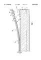
- FIG. 1is a cross-sectional view of one embodiment of the present invention taken along the line 1--1 of FIG. 2.
- FIG. 2is a perspective view of one embodiment according the present invention.
- FIG. 3is a top plan view of one embodiment according to the present invention.
- FIG. 4is a cross-sectional view of an alternate embodiment of the present invention taken along the line 4--4 of FIG. 5.
- FIG. 5is a top plan view of an alternate embodiment of the present invention.
- FIG. 6is a top plan view of the substrate contacts shown in FIG. 2.
- FIG. 7is a cross sectional view of an alternate embodiment of the present invention.
- FIG. 8is a cross sectional view of an alternate embodiment of the present invention.
- an electrostatic MEMS devicecomprises in layers, a microelectronic substrate 10, a substrate electrode 20, a substrate insulator 30, and a moveable composite 50.
- the moveable compositeis generally planar and overlies the microelectronic substrate and substrate electrode.
- the layersare arranged and shown vertically, while the portions are disposed horizontally along the moveable composite.
- the moveable composite 50comprises multiple layers including at least one electrode layer 40 and at least one biasing layer 60.
- the moveable compositehas a fixed portion 70, a medial portion 80, and a distal portion 100.
- the fixed portionis substantially affixed to the underlying microelectronic substrate or intermediate layers.
- the medial portion and distal portionare released from the underlying substrate, and in operation preferably both portions are moveable with respect to the underlying substrate and substrate electrode.
- the medial portionextends from the fixed portion and is biased or held in position without the application of electrostatic force.
- the distal portionextends from the medial portion, and is also biased or held in position without the application of electrostatic force. However, in some embodiments, the medial portion may be held in position whether or not electrostatic force is applied, such that only the distal portion is free to move in operation.
- An air gap 120is defined between the medial portion, distal portion, and the planar surface of the underlying microelectronic substrate.
- a microelectronic substrate 10defines a planar surface 12 upon which the electrostatic MEMS device is constructed.
- the microelectronic substratecomprises a silicon wafer, although any suitable substrate material having a planar surface can be used. Other semiconductors, glass, plastics, or other suitable materials may serve as the substrate.
- An insulating layer 14overlies the planar surface of the microelectronic substrate and provides electrical isolation.
- the insulating layerpreferably comprises a non-oxidation based insulator or polymer, such as polyimide or nitride.
- oxide based insulatorscannot be used if certain acids are used in processing to remove the release layer.
- Other insulators, even oxide based insulators,may be used if release layer materials and compatible acids or etchants are used for removing the release layer. For instance, silicon dioxide could be used for the insulating layers if etchants not containing hydrofluoric acid are used.
- the insulating layeris preferably formed by depositing a suitable material on the planar surface of the microelectronic substrate.
- a substrate electrode 20is disposed as a generally planar layer affixed to at least a portion of the surface of the underlying insulating layer 14.
- the substrate electrodepreferably comprises a gold layer deposited on the top surface of the insulating layer. If the substrate electrode is formed from a layer of gold, optionally a thin layer of chromium may be deposited onto the substrate electrode layer to allow better adhesion to the insulating layer and any adjacent materials. Alternatively, other metallic or conductive materials may be used so long as they are not eroded by release layer processing operations.
- a second insulating layer 30is deposited on the substrate electrode 20 to electrically isolate the substrate electrode and prevent electrical shorting.
- the insulating layerseparates the substrate electrode from the electrode layer of the moveable composite.
- the second insulating layerprovides a dielectric layer of predetermined thickness between the substrate electrode 20 and the moveable composite, including the moveable electrode 40.
- the second insulating layer 30preferably comprises polyimide, although other dielectric insulators or polymers tolerant of release layer processing may also be used.
- the second insulating layer 30has a generally planar surface 32.
- a release layeris first deposited on the planar surface 32 in the area underneath the medial and distal portions of the overlying moveable composite, occupying the space shown as the air gap 120.
- the release layeris only applied to areas below moveable composite portions not being affixed to the underlying planar surface.
- the release layercomprises an oxide or other suitable material that may be etched away when acid is applied thereto.
- the release layermay be removed through standard microengineering acidic etching techniques, such as a hydrofluoric acid etch. When the release layer has been removed, the medial and distal portions of moveable composite 50 are separated from the underlying planar surface 32, creating the air gap 120 therebetween.
- the shape of the air gapis determined according to the bias provided to the distal portion and/or medial portion of the moveable composite when no electrostatic force is applied.
- the air gapdecreases and gradually ends where the fixed portion of the moveable composite contacts the underlying substrate, as shown in FIG. 7.
- the air gapdecreases, has a generally constant width, and then ends abruptly where the fixed portion contacts the underlying substrate.
- the medial portion in this Figurehas a generally cantilevered part overlying the substrate proximate the fixed portion.
- the layers of the moveable composite 50generally overlie planar surface 32.
- Known integrated circuit manufacturing processesare used to construct the layers comprising moveable composite 50.
- two layerscomprise the moveable composite 50, one layer of moveable electrode 40 and one layer of polymer film 60 disposed on either side of the moveable electrode.
- the layer of polymer filmpreferably comprises the biasing layer used to hold the moveable composite in a given position with respect to the underlying planar surface, absent electrostatic forces.
- at least one of the layers comprising the moveable compositeis formed from a flexible material, for instance flexible polymers and/or flexible conductors may be used.
- a first layer of polymer filmcan be applied overlying at least part of the area defined by the release layer and the exposed planar surface 32, to insulate the moveable electrode 40 layer from the underlying substrate.
- a layer of polymer filmsuch as polymer film 60 shown as the top layer of the moveable composite 50, can be used as the first layer of polymer film. While polyimide is preferred for the polymer film layer, many other flexible polymers suitable for release layer fabrication processes may be used.
- Moveable electrode 40preferably comprising a layer of flexible conductor material, is deposited overlying the planar surface 32.
- the moveable electrodemay be deposited directly upon the planar surface or over an optional first layer of polymer film, as needed.
- the moveable electrode 40preferably comprises gold, although other acid tolerant yet flexible conductors, such as conductive polymer film, may be used.
- the surface area and/or configuration of moveable electrode 40can be varied as required to create the desired electrostatic forces to operate the high voltage MEMS device.
- a second layer of polymer film 60is applied overlying at least part of the moveable electrode layer.
- a flexible polymersuch as polyimide is preferred for the second polymer film layer.
- a thin layer of chromiummay be deposited onto the moveable electrode layer to allow better adhesion of the gold layer to the adjacent materials, such as to one or more layers of polymer film.
- the number of layers, thickness of layers, arrangement of layers, and choice of materials used in the moveable compositemay be selected to bias the moveable composite as required.
- the distal portion and/or the medial portioncan be biased as they extend from the fixed portion.
- the biased position of the medial and distal portionscan be customized individually or collectively to provide a desired separation from the underlying planar surface and the substrate electrode.
- the distal and medial portionscan be biased to remain parallel to the underlying planar surface.
- the distal and medial portionscan be biased to alter the separation from the underlying planar surface by curling toward or curling away from the underlying planar surface.
- the distal portion and optionally the medial portionare biased to curl away from the underlying substrate and alter the separation therefrom.
- more than one polymer film layermay be used, and that the films may be disposed on either side or both sides of the moveable electrode.
- At least one of the layers comprising the moveable compositecan function as a composite biasing layer used to bias or urge the moveable composite to curl as required.
- the medial portion 80 and distal portion 100are biased to curl away from the underlying surface 32, after the release layer has been removed.
- Providing differential thermal coefficients of expansion between the layers comprising the moveable compositecan create bias. Assuming an increase in temperature, the moveable composite will curl toward the layer having the lower thermal coefficient of expansion because the layers accordingly expand at different rates. As such, the moveable composite having two layers with different thermal coefficients of expansion will curl toward the layer having a lower thermal coefficient of expansion as the temperature rises.
- two polymer film layers having different thermal coefficients of expansioncan be used in tandem with an electrode layer to bias the moveable composite as necessary.
- the flexible compositecan be curled by creating intrinsic mechanical stresses in the layers included therein.
- sequential temperature changescan be used to curl the flexible composite.
- the polymer filmcan be deposited as a liquid and then cured by elevated temperatures so that it forms a solid polymer layer.
- a polymer having a higher thermal coefficient of expansion than the electrode layercan be used.
- the polymer layer and electrode layerare cooled, creating stresses due to differences in the thermal coefficients of expansion.
- the flexible compositecurls because the polymer layer shrinks faster than the electrode layer.
- the relative thickness of the layers comprising the moveable composite and the order in which the layers are arrangedcan be selected to create bias.
- two or more polymer films of different thicknesscan be used on either side of the electrode layer for biasing purposes.
- the thickness of the moveable electrode layercan also be selected to provide bias.
- the medial portion and distal portioncan be positionally biased and urged to curl with respect to the microelectronic substrate and substrate electrode.
- the distal portion of the moveable compositecurls out of the plane defined by the upper surface of the moveable composite when no electrostatic force is created between the substrate electrode and the composite electrode layer.
- the medial portion, the distal portion, or bothcan be biased to curl with any selected radius of curvature along the span of the portion, such as a variable or constant radius of curvature.
- the MEMS deviceis further adapted to function as an electrostatically operated high voltage switch or relay that is arc resistant.
- First and second contact setsare provided in the MEMS device, each contact set comprising one or more pairs of mating contacts.
- contact set 22 and 23comprise one contact pair
- contact set 26 and 27comprise another contact pair.
- Each contact sethas at least one composite contact attached to the moveable composite, i.e., composite contacts 23 and 27, and at least one substrate contact attached to the substrate, i.e., substrate contacts 22 and 26, arranged to mate with the corresponding composite contact to close an electrical circuit.
- first contact set 22, 23is disposed closer to the distal portion 100 of the moveable composite than the other contact set 26, 27, as shown in FIG. 1.
- first contact setis more proximate the distal portion of the moveable composite, while the second contact set is more proximate the fixed portion of the moveable composite.
- the first contact setis the contact set that is electrically connected last in time as the moveable composite is attracted to and rests upon planar surface 32 of the underlying substrate, and is electrically disconnected first in time as the moveable composite curls up from the planar surface and reassumes the biased position shown in FIG. 1.
- the second contact setcomprises an array of at least two contact sets. As shown in FIGS. 2 and 3, multiple contacts can be provided within a contact set. Contacts 27, 28, and 29 are adapted to connect with contacts 26, 24, and 25, respectively, when the moveable composite is attracted to and contacts the substrate surface.
- the second contact setcan comprise one of several different arrays of at least two contact sets.
- the second contact setcan be arranged to electrically disconnect all contacts within the contact set generally simultaneously when the distal portion of the moveable composite separates from the substrate surface.
- the arrangement shown in FIG. 2is the preferred embodiment, wherein groups of two substrate contacts and two composite contacts are interconnected such that the composite contacts act as shorting bars.
- Groups of contactsare combined in series and parallel to connect the contacts relatively sequentially or relatively simultaneously as required.
- contacts used as shorting barscan be electrically isolated from each other or electrically connected together as necessary to serve a particular application.
- the contact pairs as shown in FIG. 1require making wiring interconnections to each composite contact if an adjacent composite contact is not available to provide a return path for electrical current.
- contacts within the second contact setcan be connected in series, in parallel, or both.
- the first contact setcomprises a single contact pair.
- Another advantageous embodimentprovides the first contact set electrically connected in parallel with the second contact set, as shown in FIGS. 4-6.
- the multiple contacts of the second contact setmay have higher electrical resistance, but when connected in parallel with the first contact set having a lower resistance, the effective "on" resistance of the parallel first and second contact sets is reduced when the moveable composite is attracted to and contacts the underlying substrate.
- at least one of the first and second contact setscomprises a pair of contacts attached to the substrate.
- the contact setsfurther include a single large contact or electrically connected contacts attached to the moveable composite, such that the pair of contacts attached to the substrate can be electrically connected by the moveable composite contact.
- a single contact124 in FIGS. 4-5 and 122 in FIGS. 7-8
- the T-shaped composite contact 124 in FIG. 5interconnects substrate contacts 22 and 26, or an array of substrate contacts as shown in FIG. 2.
- contacts comprising the first and second setsmay be disposed on the moveable composite, the substrate, or both.
- each substrate contactis preferably formed from a metallization layer, such as gold.
- a metallization layersuch as gold.
- gold contactsa thin layer of chromium may be deposited onto the gold contacts to allow better adhesion of the gold layer to the adjacent materials.
- other metallic or conductive materialscan be used so long as they are not eroded by processing used to remove the release layer.
- at least one of the contact setsis electrically isolated and insulated from the substrate electrode 20 and any other substrate contacts, such that arcing and other high voltage problems are minimized.
- insulating layer 14is provided to surround and insulate substrate contacts 22 and 26 as shown in FIG. 1.
- the substrate electrodepreferably surrounds at least part of the insulating gap around each substrate contact, such that the moveable composite can be electrostatically attracted over, and firmly contact the entire surface area of the substrate contact.
- a contact setincludes a composite contact
- each composite contactis disposed within the moveable electrode 40 layer and attached to the moveable composite.
- One or more composite contactsare formed from the moveable composite electrode layer, as shown in FIG. 1.
- Insulating gapssuch as 41, 42, and 43, serve to electrically isolate the composite contacts from the moveable electrode. While the insulating gaps are preferably filled with air, many other suitable insulators can be used.
- the layer of polymer film 60serves as an insulator.
- at least one of the composite contacts within a contact setis electrically isolated from the substrate electrode 20.
- One or more insulatorscan be used in combination to electrically insulate the composite contact(s) accordingly.
- an insulating layer 30, a layer of polymer film 60, or bothcan be selectively applied as needed to electrically isolate the moveable composite and one or more composite contacts from the underlying substrate electrode 20.
- a composite contactcan be adapted to extend through polymer film layer 60.
- at least a portion of the composite contacts 23 and 27protrudes above the upper polymer film layer so as to provide one or more electrical connections.
- a single composite shorting bar 124can protrude through the polymer film layer to provide an electrical connection between contact sets while also functioning as a component of each contact set.
- a single composite shorting bar 122can protrude through the polymer film layer to provide an electrical connection 123.
- Metal linesmay be deposited for interconnection.
- substrate and composite contact setscan be varied as required for different switch or relay applications.
- two or more mating contacts setscan be disposed along the length (from fixed to distal) of the moveable composite, such that some contact sets are mated before others as the composite is attracted to the substrate.
- substrate contact 26will mate with its composite contact before substrate contact 22 as the moveable composite is attracted to the underlying substrate.
- two or more contact setscan be disposed along the width of the moveable composite, such that two or more contacts within a set are mated at generally the same time.
- substrate contacts 24, 25 and 26will mate with their composite contacts generally simultaneously, before substrate contact 22, as the composite is attracted to the substrate.
- contact sets within the pluralitycan be disposed to mate both in parallel and in series as the moveable composite is attracted thereto.
- Some embodiments of the MEMS device according to the present inventionfurther comprise a source of electrical energy and an optional switching device. See the example in FIG. 4.
- the source of electrical energycan be any voltage source, current source, or electrical storage device, such as a battery, charged capacitor, energized inductor, or the like.
- the switching devicecan be any electrical switch or other semiconductor device used for selectively making and breaking an electrical connection.
- a source of electrical energy 130is connected to the substrate electrode, composite electrode, or both, of the MEMS device.
- a switching device 133may also be connected in circuit with the source of electrical energy. In operation, when no electrostatic force is applied the distal portion and optionally the medial portion of the moveable composite are biased in an open position, as shown in FIG. 1.
- the application of electrical charge to the substrate electrode and moveable composite electrodecreates an electrostatic force between them, attracting the moveable electrode to the substrate electrode as shown in FIG. 4. This causes the biased portion(s) to uncurl and conform to the surface of the microelectronic substrate, interconnecting the composite contact(s) and substrate contact(s) within each contact set.
- a source of electrical energy 135can be connected to the substrate contact, composite contact, or both, of the MEMS device, in circuit with one or more devices, for example D1, shown as 137.
- the source of electrical energy and one or more devices such as D1can be selectively connected when the substrate contact(s) and composite contact(s) are electrically connected in response to the application of electrostatic forces.
- an electrical loadis connected to the substrate contacts, and the composite contact is used as a shorting bar for interconnecting the electrical load.
- the contact set more proximate the fixed portion 70will be connected first in time.
- the moveable compositeis raised and the contacts are all open.
- the moveable compositeuncurls and contacts 26 and 27 will be connected before contacts 22 and 23.
- the distal and medial portions of the moveable compositecan reassume the biased position. As the distal portion curls away, contacts 22 and 23 separate first, followed by contacts 26 and 27.
- the MEMS electrostatic switch and relay according to the present inventioncan switch voltages from 0.1 to 400 volts, while operating with electrostatic voltages in the range of 30 to 80 volts. Depending on the amount of electrical current switched and the device geometry, other switching voltages and operating voltages can be provided.
- FIGS. 2-8illustrate use of the multiple contact sets in parallel to minimize arcing by increasing the number of contact sets while also minimizing contact set resistance.
- substrate contacts 24A-24B, 25A-25B, and 26A-26Bare connected in series, and are normally open when the flexible composite is biased to its raised position, as shown.
- Composite contacts 27, 28 and 29are shorting contacts that electrically close the substrate contacts. This reduces arcing because each arc requires approximately 16 volts to occur, and multiple contacts will require a proportionally higher voltage to form an arc.
- the switch represented by FIGS. 2 and 6comprises six sets of contacts and will require approximately 96 volts to arc.
- all of the second contact setsi.e., 24-26
- all of the second contact setsopen essentially simultaneously, and this is more likely with a MEMS device. It is desirable to orient the contact sets parallel to the distal end of the moveable composite, as shown, in a direction that is generally parallel to the trough formed in the moveable composite as it curls upward.
- a single set of contacts 22A-22Bis electrically and physically parallel to the multiple contact set, ensuring that the single set will open and close in sequence with the multiple set.
- the single setis closer to the distal end of the moveable composite.
- the multicontact sets 24, 25, 26close first, quickly followed by contact set 22. This lowers the resistance of the entire switch, as represented by pads 34, 35 in FIG. 6.
- the single contact shorting bar 124 shown in FIG. 5can be used in the same sequential manner with the substrate contacts shown in FIG. 6.
- the method for using the MEMS devicecomprises the step of selectively generating an electrostatic force between the substrate electrode and the electrode layer of the moveable composite.
- the methodcomprises the step of moving the moveable composite toward the microelectronic substrate.
- the methodcomprises the step of electrically connecting the contacts of the first and second contact sets. After the electrically connecting step, the method can comprise the steps of discontinuing the electrostatic force, separating the moveable composite from the substrate, and sequentially disconnecting the contacts of the first and second contact sets.
- the step of selectively generating an electrostatic forcecan comprise applying a voltage potential between the substrate electrode and the electrode layer of the moveable composite.
- the step of moving the moveable compositemay comprise uncurling the moveable composite to lie generally parallel to the microelectronic substrate.
- the step of electrically connectingcan comprise electrically connecting the contacts on the moveable composite with contacts on the substrate.
- the step of separating the moveable composite from the substratecan comprise moving the moveable composite away from the substrate with a pivoting or curling displacement.
- the methodcan provide multiple steps as the first and second contact sets are disconnected.
- the step of separating the moveable composite from the substratemay comprise moving the moveable composite away from the substrate, with the distal end separating from the substrate prior to the remainder of the moveable composite separating from the substrate.
- This sequentially disconnecting stepcan comprise electrically disconnecting the contacts of the first set prior to electrically disconnecting the contacts of the second contact set.
- the step of sequentially disconnectingmay comprise disconnecting the contacts of the first and second contact sets generally simultaneously, wherein the second contact set comprises a plurality of contacts.
- the step of sequentially disconnecting the first and second contact setscan comprise disconnecting a single contact set within the first contact set. Further, the step of sequentially disconnecting can comprise disconnecting the contacts of the first contact set prior to disconnecting all contacts of the second contact set generally simultaneously.
- the step of separating the moveable composite from the substratecan comprise curling the moveable composite away from the substrate. In this case, the step of curling can further comprise the step of sequentially disconnecting the contacts of the first contact set prior to disconnecting the contacts of the second contact set.
Landscapes
- Micromachines (AREA)
Abstract
Description
Claims (43)
Priority Applications (6)
| Application Number | Priority Date | Filing Date | Title |
|---|---|---|---|
| US09/345,300US6057520A (en) | 1999-06-30 | 1999-06-30 | Arc resistant high voltage micromachined electrostatic switch |
| JP2001508469AJP4030760B2 (en) | 1999-06-30 | 2000-05-04 | Arc-resistant high-voltage electrostatic switch |
| AU48191/00AAU4819100A (en) | 1999-06-30 | 2000-05-04 | Arc resistant high voltage micromachined electrostatic switch |
| PCT/US2000/012142WO2001003152A1 (en) | 1999-06-30 | 2000-05-04 | Arc resistant high voltage micromachined electrostatic switch |
| EP00930355AEP1196932A1 (en) | 1999-06-30 | 2000-05-04 | Arc resistant high voltage micromachined electrostatic switch |
| TW089109155ATW449762B (en) | 1999-06-30 | 2000-05-12 | Arc resistant high voltage micromachined electrostatic switch |
Applications Claiming Priority (1)
| Application Number | Priority Date | Filing Date | Title |
|---|---|---|---|
| US09/345,300US6057520A (en) | 1999-06-30 | 1999-06-30 | Arc resistant high voltage micromachined electrostatic switch |
Publications (1)
| Publication Number | Publication Date |
|---|---|
| US6057520Atrue US6057520A (en) | 2000-05-02 |
Family
ID=23354460
Family Applications (1)
| Application Number | Title | Priority Date | Filing Date |
|---|---|---|---|
| US09/345,300Expired - LifetimeUS6057520A (en) | 1999-06-30 | 1999-06-30 | Arc resistant high voltage micromachined electrostatic switch |
Country Status (6)
| Country | Link |
|---|---|
| US (1) | US6057520A (en) |
| EP (1) | EP1196932A1 (en) |
| JP (1) | JP4030760B2 (en) |
| AU (1) | AU4819100A (en) |
| TW (1) | TW449762B (en) |
| WO (1) | WO2001003152A1 (en) |
Cited By (119)
| Publication number | Priority date | Publication date | Assignee | Title |
|---|---|---|---|---|
| US6127744A (en)* | 1998-11-23 | 2000-10-03 | Raytheon Company | Method and apparatus for an improved micro-electrical mechanical switch |
| US6191671B1 (en)* | 1997-08-22 | 2001-02-20 | Siemens Electromechanical Components Gmbh & Co. Kg | Apparatus and method for a micromechanical electrostatic relay |
| US6229684B1 (en)* | 1999-12-15 | 2001-05-08 | Jds Uniphase Inc. | Variable capacitor and associated fabrication method |
| US6233088B1 (en)* | 1998-03-17 | 2001-05-15 | Mcnc | Methods for modulating a radiation signal |
| US6327909B1 (en)* | 1999-11-30 | 2001-12-11 | Xerox Corporation | Bistable mechanical sensors capable of threshold detection and automatic elimination of excessively high amplitude data |
| WO2002021568A2 (en) | 2000-09-01 | 2002-03-14 | Mcnc | Distributed mems electrostatic pumping devices |
| US6373682B1 (en)* | 1999-12-15 | 2002-04-16 | Mcnc | Electrostatically controlled variable capacitor |
| US6384353B1 (en)* | 2000-02-01 | 2002-05-07 | Motorola, Inc. | Micro-electromechanical system device |
| WO2002039472A1 (en)* | 2000-11-09 | 2002-05-16 | Raytheon Company | Micro-relay contact structure for rf applications |
| US6396368B1 (en)* | 1999-11-10 | 2002-05-28 | Hrl Laboratories, Llc | CMOS-compatible MEM switches and method of making |
| US6407482B2 (en)* | 1996-08-27 | 2002-06-18 | Omron Corporation | Micro-relay and method for manufacturing the same |
| US20020096776A1 (en)* | 2001-01-24 | 2002-07-25 | Hrl Laboratories, Llc | Integrated circuits protected against reverse engineering and method for fabricating the same using an apparent metal contact line terminating on field oxide |
| US20020101907A1 (en)* | 2001-01-26 | 2002-08-01 | Dent Paul W. | Adaptive antenna optimization network |
| US6438521B1 (en)* | 1998-09-17 | 2002-08-20 | Canon Kabushiki Kaisha | Speech recognition method and apparatus and computer-readable memory |
| US6483056B2 (en)* | 2000-10-27 | 2002-11-19 | Daniel J Hyman | Microfabricated relay with multimorph actuator and electrostatic latch mechanism |
| US20020173131A1 (en)* | 2000-10-25 | 2002-11-21 | Clark William M. | Implanted hidden interconnections in a semiconductor device for preventing reverse engineering |
| US20020182091A1 (en)* | 2001-05-31 | 2002-12-05 | Potter Michael D. | Micro fluidic valves, agitators, and pumps and methods thereof |
| US6504118B2 (en)* | 2000-10-27 | 2003-01-07 | Daniel J Hyman | Microfabricated double-throw relay with multimorph actuator and electrostatic latch mechanism |
| US6507475B1 (en)* | 2000-06-27 | 2003-01-14 | Motorola, Inc. | Capacitive device and method of manufacture |
| WO2003026369A1 (en)* | 2001-09-17 | 2003-03-27 | John Stafford | Latching micro magnetic relay packages and methods of packaging |
| US20030058069A1 (en)* | 2001-09-21 | 2003-03-27 | Schwartz Robert N. | Stress bimorph MEMS switches and methods of making same |
| WO2003043044A1 (en)* | 2001-11-09 | 2003-05-22 | Conventor, Incorporated | Mems device having a trilayered beam and related methods |
| US20030123798A1 (en)* | 2001-12-10 | 2003-07-03 | Jianjun Zhang | Wavelength-selective optical switch with integrated Bragg gratings |
| US20030138986A1 (en)* | 2001-09-13 | 2003-07-24 | Mike Bruner | Microelectronic mechanical system and methods |
| US6608268B1 (en)* | 2002-02-05 | 2003-08-19 | Memtronics, A Division Of Cogent Solutions, Inc. | Proximity micro-electro-mechanical system |
| US6639325B1 (en)* | 1999-07-29 | 2003-10-28 | Tyco Electronics Logistics Ag | Microelectromechanic relay and method for the production thereof |
| US6646215B1 (en) | 2001-06-29 | 2003-11-11 | Teravicin Technologies, Inc. | Device adapted to pull a cantilever away from a contact structure |
| US20030214002A1 (en)* | 2002-05-14 | 2003-11-20 | Hrl Laboratories, Llc | Integrated circuit with reverse engineering protection |
| US6654155B2 (en) | 2000-11-29 | 2003-11-25 | Xerox Corporation | Single-crystal-silicon ribbon hinges for micro-mirror and MEMS assembly on SOI material |
| US20030222341A1 (en)* | 2002-04-01 | 2003-12-04 | Oberhardt Bruce J. | Systems and methods for cooling microelectronic devices using oscillatory devices |
| US20030235932A1 (en)* | 2002-05-28 | 2003-12-25 | Silicon Light Machines | Integrated driver process flow |
| US6671078B2 (en) | 2001-05-23 | 2003-12-30 | Axsun Technologies, Inc. | Electrostatic zipper actuator optical beam switching system and method of operation |
| US20040012067A1 (en)* | 2001-06-15 | 2004-01-22 | Hrl Laboratories, Llc | Programmable connector/isolator and double polysilicon layer CMOS process with buried contact using the same |
| US6701779B2 (en) | 2002-03-21 | 2004-03-09 | International Business Machines Corporation | Perpendicular torsion micro-electromechanical switch |
| US6707355B1 (en) | 2001-06-29 | 2004-03-16 | Teravicta Technologies, Inc. | Gradually-actuating micromechanical device |
| US6707591B2 (en) | 2001-04-10 | 2004-03-16 | Silicon Light Machines | Angled illumination for a single order light modulator based projection system |
| US6714337B1 (en) | 2002-06-28 | 2004-03-30 | Silicon Light Machines | Method and device for modulating a light beam and having an improved gamma response |
| US6712480B1 (en) | 2002-09-27 | 2004-03-30 | Silicon Light Machines | Controlled curvature of stressed micro-structures |
| US20040061186A1 (en)* | 2002-09-27 | 2004-04-01 | Lap-Wai Chow | Conductive channel pseudo block process and circuit to inhibit reverse engineering |
| US6728023B1 (en) | 2002-05-28 | 2004-04-27 | Silicon Light Machines | Optical device arrays with optimized image resolution |
| US6740942B2 (en)* | 2001-06-15 | 2004-05-25 | Hrl Laboratories, Llc. | Permanently on transistor implemented using a double polysilicon layer CMOS process with buried contact |
| US20040099912A1 (en)* | 2002-11-22 | 2004-05-27 | Hrl Laboratories, Llc. | Use of silicon block process step to camouflage a false transistor |
| US6743989B2 (en) | 2000-08-21 | 2004-06-01 | Abb Research Ltd. | Microswitch |
| US6745567B1 (en)* | 2001-12-28 | 2004-06-08 | Zyvex Corporation | System and method for positional movement of microcomponents |
| US6747781B2 (en) | 2001-06-25 | 2004-06-08 | Silicon Light Machines, Inc. | Method, apparatus, and diffuser for reducing laser speckle |
| US20040112732A1 (en)* | 2001-04-17 | 2004-06-17 | Leif Bergstedt | Printed circuit board intergrated switch |
| US6756545B2 (en)* | 2000-11-29 | 2004-06-29 | Xerox Corporation | Micro-device assembly with electrical capabilities |
| US6764875B2 (en) | 1998-07-29 | 2004-07-20 | Silicon Light Machines | Method of and apparatus for sealing an hermetic lid to a semiconductor die |
| US20040145271A1 (en)* | 2001-10-26 | 2004-07-29 | Potter Michael D | Electrostatic based power source and methods thereof |
| US20040144998A1 (en)* | 2002-12-13 | 2004-07-29 | Lap-Wai Chow | Integrated circuit modification using well implants |
| US20040146240A1 (en)* | 2001-10-22 | 2004-07-29 | Jianjun Zhang | Waveguide grating-based wavelength selective switch actuated by thermal mechanism |
| US20040155555A1 (en)* | 2001-10-26 | 2004-08-12 | Potter Michael D. | Electrostatic based power source and methods thereof |
| US6782205B2 (en) | 2001-06-25 | 2004-08-24 | Silicon Light Machines | Method and apparatus for dynamic equalization in wavelength division multiplexing |
| US6787438B1 (en) | 2001-10-16 | 2004-09-07 | Teravieta Technologies, Inc. | Device having one or more contact structures interposed between a pair of electrodes |
| US6791191B2 (en) | 2001-01-24 | 2004-09-14 | Hrl Laboratories, Llc | Integrated circuits protected against reverse engineering and method for fabricating the same using vias without metal terminations |
| US6798315B2 (en) | 2001-12-04 | 2004-09-28 | Mayo Foundation For Medical Education And Research | Lateral motion MEMS Switch |
| US6801354B1 (en) | 2002-08-20 | 2004-10-05 | Silicon Light Machines, Inc. | 2-D diffraction grating for substantially eliminating polarization dependent losses |
| US6800238B1 (en) | 2002-01-15 | 2004-10-05 | Silicon Light Machines, Inc. | Method for domain patterning in low coercive field ferroelectrics |
| US6806997B1 (en) | 2003-02-28 | 2004-10-19 | Silicon Light Machines, Inc. | Patterned diffractive light modulator ribbon for PDL reduction |
| US20040207499A1 (en)* | 2001-03-12 | 2004-10-21 | Tsung-Yuan Hsu | Torsion spring for electro-mechanical switches and a cantilever-type RF micro-electromechanical switch incorporating the torsion spring |
| US6813059B2 (en) | 2002-06-28 | 2004-11-02 | Silicon Light Machines, Inc. | Reduced formation of asperities in contact micro-structures |
| US6822797B1 (en) | 2002-05-31 | 2004-11-23 | Silicon Light Machines, Inc. | Light modulator structure for producing high-contrast operation using zero-order light |
| US6829258B1 (en) | 2002-06-26 | 2004-12-07 | Silicon Light Machines, Inc. | Rapidly tunable external cavity laser |
| US6829077B1 (en) | 2003-02-28 | 2004-12-07 | Silicon Light Machines, Inc. | Diffractive light modulator with dynamically rotatable diffraction plane |
| US6829092B2 (en) | 2001-08-15 | 2004-12-07 | Silicon Light Machines, Inc. | Blazed grating light valve |
| US20050018964A1 (en)* | 2003-07-24 | 2005-01-27 | Yu Chen | Compensation of Bragg wavelength shift in a grating assisted direct coupler |
| US20050044955A1 (en)* | 2003-08-29 | 2005-03-03 | Potter Michael D. | Methods for distributed electrode injection and systems thereof |
| US20050047010A1 (en)* | 2001-08-16 | 2005-03-03 | Nobuyuki Ishiwata | Thin film electromagnet and switching device comprising it |
| US6865346B1 (en) | 2001-06-05 | 2005-03-08 | Silicon Light Machines Corporation | Fiber optic transceiver |
| US6872984B1 (en) | 1998-07-29 | 2005-03-29 | Silicon Light Machines Corporation | Method of sealing a hermetic lid to a semiconductor die at an angle |
| US20050093141A1 (en)* | 2002-01-18 | 2005-05-05 | Ralf Strumpler | Micro-electromechanical system and method for production thereof |
| US6908201B2 (en) | 2002-06-28 | 2005-06-21 | Silicon Light Machines Corporation | Micro-support structures |
| US6922273B1 (en) | 2003-02-28 | 2005-07-26 | Silicon Light Machines Corporation | PDL mitigation structure for diffractive MEMS and gratings |
| US6922272B1 (en) | 2003-02-14 | 2005-07-26 | Silicon Light Machines Corporation | Method and apparatus for leveling thermal stress variations in multi-layer MEMS devices |
| US20050167769A1 (en)* | 2002-04-30 | 2005-08-04 | Palo Alto Research Center Incorporated | Electrode design and positioning for controlled movement of a moveable electrode and associated support structure |
| US6928207B1 (en) | 2002-12-12 | 2005-08-09 | Silicon Light Machines Corporation | Apparatus for selectively blocking WDM channels |
| US6927891B1 (en) | 2002-12-23 | 2005-08-09 | Silicon Light Machines Corporation | Tilt-able grating plane for improved crosstalk in 1×N blaze switches |
| US6934070B1 (en) | 2002-12-18 | 2005-08-23 | Silicon Light Machines Corporation | Chirped optical MEM device |
| US20050196099A1 (en)* | 2004-03-04 | 2005-09-08 | Rosemount Inc. | MEMS-based actuator devices using electrets |
| US6947613B1 (en) | 2003-02-11 | 2005-09-20 | Silicon Light Machines Corporation | Wavelength selective switch and equalizer |
| US20050206243A1 (en)* | 2004-02-04 | 2005-09-22 | Stmicroelectronics S.A. | Microelectromechanical system able to switch between two stable positions |
| US20050205966A1 (en)* | 2004-02-19 | 2005-09-22 | Potter Michael D | High Temperature embedded charge devices and methods thereof |
| US6956995B1 (en) | 2001-11-09 | 2005-10-18 | Silicon Light Machines Corporation | Optical communication arrangement |
| US6956878B1 (en) | 2000-02-07 | 2005-10-18 | Silicon Light Machines Corporation | Method and apparatus for reducing laser speckle using polarization averaging |
| US20050230787A1 (en)* | 2004-04-19 | 2005-10-20 | Hrl Laboratories, Llc. | Covert transformation of transistor properties as a circuit protection method |
| US20050236260A1 (en)* | 2004-01-29 | 2005-10-27 | Rolltronics Corporation | Micro-electromechanical switch array |
| US20050265720A1 (en)* | 2004-05-28 | 2005-12-01 | Peiching Ling | Wavelength division multiplexing add/drop system employing optical switches and interleavers |
| US6987600B1 (en) | 2002-12-17 | 2006-01-17 | Silicon Light Machines Corporation | Arbitrary phase profile for better equalization in dynamic gain equalizer |
| US7027202B1 (en) | 2003-02-28 | 2006-04-11 | Silicon Light Machines Corp | Silicon substrate as a light modulator sacrificial layer |
| WO2005104717A3 (en)* | 2004-04-23 | 2006-04-27 | David E Dausch | Flexible electrostatic actuator |
| US7042611B1 (en) | 2003-03-03 | 2006-05-09 | Silicon Light Machines Corporation | Pre-deflected bias ribbons |
| US7054515B1 (en) | 2002-05-30 | 2006-05-30 | Silicon Light Machines Corporation | Diffractive light modulator-based dynamic equalizer with integrated spectral monitor |
| US7057819B1 (en) | 2002-12-17 | 2006-06-06 | Silicon Light Machines Corporation | High contrast tilting ribbon blazed grating |
| US7057795B2 (en) | 2002-08-20 | 2006-06-06 | Silicon Light Machines Corporation | Micro-structures with individually addressable ribbon pairs |
| US20060131150A1 (en)* | 2004-12-21 | 2006-06-22 | Fujitsu Component Limited | Switch device |
| US7068372B1 (en) | 2003-01-28 | 2006-06-27 | Silicon Light Machines Corporation | MEMS interferometer-based reconfigurable optical add-and-drop multiplexor |
| US20060180756A1 (en)* | 2005-02-14 | 2006-08-17 | Harris Corporation | High energy photon detector and power source with MEMS switch |
| US20060227489A1 (en)* | 2003-08-30 | 2006-10-12 | Bunyan Robert J T | Micro electromechanical system switch |
| US7177081B2 (en) | 2001-03-08 | 2007-02-13 | Silicon Light Machines Corporation | High contrast grating light valve type device |
| US20070074731A1 (en)* | 2005-10-05 | 2007-04-05 | Nth Tech Corporation | Bio-implantable energy harvester systems and methods thereof |
| US7217582B2 (en) | 2003-08-29 | 2007-05-15 | Rochester Institute Of Technology | Method for non-damaging charge injection and a system thereof |
| US20070126536A1 (en)* | 2005-12-02 | 2007-06-07 | Palo Alto Research Center Incorporated | Electromechanical switch |
| US7242063B1 (en) | 2004-06-29 | 2007-07-10 | Hrl Laboratories, Llc | Symmetric non-intrusive and covert technique to render a transistor permanently non-operable |
| US7286764B1 (en) | 2003-02-03 | 2007-10-23 | Silicon Light Machines Corporation | Reconfigurable modulator-based optical add-and-drop multiplexer |
| US20080047816A1 (en)* | 2006-08-25 | 2008-02-28 | Kabushiki Kaisha Toshiba | Mems switch |
| US20080055815A1 (en)* | 2006-08-18 | 2008-03-06 | Interuniversitair Microelektronica Centrum (Imec) Vzw | MEMS variable capacitor and method for producing the same |
| US20080079082A1 (en)* | 2006-09-28 | 2008-04-03 | Hrl Laboratories, Llc | Programmable connection and isolation of active regions in an integrated circuit using ambiguous features to confuse a reverse engineer |
| US20080087530A1 (en)* | 2006-10-12 | 2008-04-17 | Innovative Micro Technology | Contact electrode for microdevices and etch method of manufacture |
| US7391973B1 (en) | 2003-02-28 | 2008-06-24 | Silicon Light Machines Corporation | Two-stage gain equalizer |
| US20080238257A1 (en)* | 2007-03-27 | 2008-10-02 | Kabushiki Kaisha Toshiba | Mems device and portable communication terminal with said mems device |
| US20080272867A1 (en)* | 2000-11-29 | 2008-11-06 | Microassembly Technologies, Inc. | Mems device with integral packaging |
| CN100451737C (en)* | 2004-04-23 | 2009-01-14 | 研究三角协会 | Flexible electrostatic actuator |
| EP1626421A4 (en)* | 2003-05-20 | 2009-02-11 | Fujitsu Ltd | DEVICE WITH ELECTRICAL CONTACTS |
| GB2452096A (en)* | 2007-08-22 | 2009-02-25 | Sunonwealth Electr Mach Ind Co | Micro actuator contact. |
| US20100025206A1 (en)* | 2006-12-12 | 2010-02-04 | Nxp, B.V. | Mems device with controlled electrode off-state position |
| US7754986B1 (en)* | 2007-02-27 | 2010-07-13 | National Semiconductor Corporation | Mechanical switch that reduces the effect of contact resistance |
| US20110209976A1 (en)* | 2010-03-01 | 2011-09-01 | Visteon Global Technologies, Inc. | Method for implementing capacitive sensing in the presence of conductive decorative materials |
| US8168120B1 (en) | 2007-03-06 | 2012-05-01 | The Research Foundation Of State University Of New York | Reliable switch that is triggered by the detection of a specific gas or substance |
| US11092977B1 (en) | 2017-10-30 | 2021-08-17 | Zane Coleman | Fluid transfer component comprising a film with fluid channels |
Families Citing this family (9)
| Publication number | Priority date | Publication date | Assignee | Title |
|---|---|---|---|---|
| US6571029B1 (en) | 2001-02-13 | 2003-05-27 | Omm, Inc. | Method for determining and implementing electrical damping coefficients |
| US6556739B1 (en) | 2001-02-13 | 2003-04-29 | Omm, Inc. | Electronic damping of MEMS devices using a look-up table |
| US7053519B2 (en)* | 2002-03-29 | 2006-05-30 | Microsoft Corporation | Electrostatic bimorph actuator |
| US7202764B2 (en)* | 2003-07-08 | 2007-04-10 | International Business Machines Corporation | Noble metal contacts for micro-electromechanical switches |
| JP4739173B2 (en)* | 2006-12-07 | 2011-08-03 | 富士通株式会社 | Micro switching element |
| US8977255B2 (en) | 2007-04-03 | 2015-03-10 | Apple Inc. | Method and system for operating a multi-function portable electronic device using voice-activation |
| RU2393573C1 (en)* | 2009-04-28 | 2010-06-27 | Общество с ограниченной ответственностью "Технос" | Contact circuit of switch |
| JP2011228355A (en)* | 2010-04-15 | 2011-11-10 | Fujitsu Ltd | Variable capacity element and method of manufacturing variable capacity element |
| JP3182209U (en)* | 2012-12-26 | 2013-03-14 | 株式会社シマノ | Bicycle control device |
Citations (82)
| Publication number | Priority date | Publication date | Assignee | Title |
|---|---|---|---|---|
| US33568A (en)* | 1861-10-29 | Improvement in plows | ||
| US33618A (en)* | 1861-10-29 | Improvement in screens of win nowing-mach in es | ||
| US33587A (en)* | 1861-10-29 | Improved stove-cover lifter and poker | ||
| US33577A (en)* | 1861-10-29 | Improvement in mode of attaching hubs to axles | ||
| US33691A (en)* | 1861-11-12 | Improvement in grain and grass harvesters | ||
| US2851618A (en)* | 1954-06-03 | 1958-09-09 | Guenther H Krawinkel | Electrostatic devices |
| US2927255A (en)* | 1954-07-02 | 1960-03-01 | Erdco Inc | Electrostatic controls |
| US2942077A (en)* | 1954-07-02 | 1960-06-21 | Erdco Inc | Electrostatic controls |
| US3772537A (en)* | 1972-10-27 | 1973-11-13 | Trw Inc | Electrostatically actuated device |
| US3917196A (en)* | 1974-02-11 | 1975-11-04 | Boeing Co | Apparatus suitable for use in orienting aircraft flight for refueling or other purposes |
| US4025193A (en)* | 1974-02-11 | 1977-05-24 | The Boeing Company | Apparatus suitable for use in orienting aircraft in-flight for refueling or other purposes |
| US4209689A (en)* | 1969-06-04 | 1980-06-24 | Hughes Aircraft Company | Laser secure communications system |
| US4361911A (en)* | 1981-05-21 | 1982-11-30 | The United States Of American As Represented By The Secretary Of The Army | Laser retroreflector system for identification of friend or foe |
| US4403166A (en)* | 1980-12-19 | 1983-09-06 | Matsushita Electric Industrial Co., Ltd. | Piezoelectric relay with oppositely bending bimorphs |
| US4447723A (en)* | 1981-09-03 | 1984-05-08 | Excellon Industries | Scanning beam reference employing a retroreflective code means |
| US4473859A (en)* | 1982-09-22 | 1984-09-25 | Piezo Electric Products, Inc. | Piezoelectric circuit breaker |
| US4480162A (en)* | 1981-03-17 | 1984-10-30 | International Standard Electric Corporation | Electrical switch device with an integral semiconductor contact element |
| US4517569A (en)* | 1982-02-17 | 1985-05-14 | The United States Of America As Represented By The Secretary Of The Army | Passive retroreflective doppler shift system |
| US4553061A (en)* | 1984-06-11 | 1985-11-12 | General Electric Company | Piezoelectric bimorph driven direct current latching relay |
| US4581624A (en)* | 1984-03-01 | 1986-04-08 | Allied Corporation | Microminiature semiconductor valve |
| US4595855A (en)* | 1984-12-21 | 1986-06-17 | General Electric Company | Synchronously operable electrical current switching apparatus |
| US4620124A (en)* | 1984-12-21 | 1986-10-28 | General Electric Company | Synchronously operable electrical current switching apparatus having increased contact separation in the open position and increased contact closing force in the closed position |
| US4620123A (en)* | 1984-12-21 | 1986-10-28 | General Electric Company | Synchronously operable electrical current switching apparatus having multiple circuit switching capability and/or reduced contact resistance |
| US4622484A (en)* | 1984-06-21 | 1986-11-11 | Nec Corporation | Piezoelectric relay with a piezoelectric longitudinal effect actuator |
| US4626698A (en)* | 1984-12-21 | 1986-12-02 | General Electric Company | Zero crossing synchronous AC switching circuits employing piezoceramic bender-type switching devices |
| US4658154A (en)* | 1985-12-20 | 1987-04-14 | General Electric Company | Piezoelectric relay switching circuit |
| US4727593A (en)* | 1981-03-25 | 1988-02-23 | Pinchas Goldstein | Passive line-of-sight optical switching apparatus |
| US4731879A (en)* | 1983-08-05 | 1988-03-15 | Messerschmitt-Boelkow-Blohm Gmbh | Remote data monitoring system |
| US4736202A (en)* | 1984-08-21 | 1988-04-05 | Bos-Knox, Ltd. | Electrostatic binary switching and memory devices |
| US4747670A (en)* | 1986-03-17 | 1988-05-31 | Display Science, Inc. | Electrostatic device and terminal therefor |
| US4777660A (en)* | 1984-11-06 | 1988-10-11 | Optelecom Incorporated | Retroreflective optical communication system |
| US4794370A (en)* | 1984-08-21 | 1988-12-27 | Bos-Knox Ltd. | Peristaltic electrostatic binary device |
| US4811246A (en)* | 1986-03-10 | 1989-03-07 | Fitzgerald Jr William M | Micropositionable piezoelectric contactor |
| US4819126A (en)* | 1988-05-19 | 1989-04-04 | Pacific Bell | Piezoelectic relay module to be utilized in an appliance or the like |
| US4826131A (en)* | 1988-08-22 | 1989-05-02 | Ford Motor Company | Electrically controllable valve etched from silicon substrates |
| US4857757A (en)* | 1984-06-29 | 1989-08-15 | Omron Tateisi Electronics Co. | Drive circuit for a two layer laminated electrostriction element |
| US4893048A (en)* | 1988-10-03 | 1990-01-09 | General Electric Company | Multi-gap switch |
| US4916349A (en)* | 1988-05-10 | 1990-04-10 | Pacific Bell | Latching piezoelectric relay |
| US4983021A (en)* | 1988-08-10 | 1991-01-08 | Fergason James L | Modulated retroreflector system |
| USRE33568E (en) | 1984-12-21 | 1991-04-09 | General Electric Company | Piezoelectric ceramic switching devices and systems and methods of making the same |
| USRE33577E (en) | 1984-12-21 | 1991-04-23 | General Electric Company | Advanced piezoceramic power switching devices employing protective gastight enclosure and method of manufacture |
| USRE33587E (en) | 1984-12-21 | 1991-05-14 | General Electric Company | Method for (prepolarizing and centering) operating a piezoceramic power switching device |
| USRE33618E (en) | 1984-12-21 | 1991-06-25 | General Electric Company | Method for initially polarizing and centering a piezoelectric ceramic switching device |
| USRE33691E (en) | 1984-12-21 | 1991-09-17 | General Electric Company | Piezoelectric ceramic switching devices and systems and method of making the same |
| US5051643A (en)* | 1990-08-30 | 1991-09-24 | Motorola, Inc. | Electrostatically switched integrated relay and capacitor |
| US5065978A (en)* | 1988-04-27 | 1991-11-19 | Dragerwerk Aktiengesellschaft | Valve arrangement of microstructured components |
| US5093600A (en)* | 1987-09-18 | 1992-03-03 | Pacific Bell | Piezo-electric relay |
| US5162691A (en)* | 1991-01-22 | 1992-11-10 | The United States Of America As Represented By The Secretary Of The Army | Cantilevered air-gap type thin film piezoelectric resonator |
| US5177331A (en)* | 1991-07-05 | 1993-01-05 | Delco Electronics Corporation | Impact detector |
| US5233459A (en)* | 1991-03-06 | 1993-08-03 | Massachusetts Institute Of Technology | Electric display device |
| US5243861A (en)* | 1990-09-07 | 1993-09-14 | Hitachi, Ltd. | Capacitive type semiconductor accelerometer |
| US5258591A (en)* | 1991-10-18 | 1993-11-02 | Westinghouse Electric Corp. | Low inductance cantilever switch |
| US5261747A (en)* | 1992-06-22 | 1993-11-16 | Trustees Of Dartmouth College | Switchable thermoelectric element and array |
| US5268696A (en)* | 1992-04-06 | 1993-12-07 | Westinghouse Electric Corp. | Slotline reflective phase shifting array element utilizing electrostatic switches |
| US5274379A (en)* | 1991-11-08 | 1993-12-28 | Her Majesty The Queen As Represented By The Minister Of National Defence Of Her Majesty's Canadian Government | Optical identification friend-or-foe |
| US5278368A (en)* | 1991-06-24 | 1994-01-11 | Matsushita Elec. Works, Ltd | Electrostatic relay |
| US5311360A (en)* | 1992-04-28 | 1994-05-10 | The Board Of Trustees Of The Leland Stanford, Junior University | Method and apparatus for modulating a light beam |
| US5355241A (en)* | 1991-12-09 | 1994-10-11 | Kelley Clifford W | Identification friend or foe discriminator |
| US5367136A (en)* | 1993-07-26 | 1994-11-22 | Westinghouse Electric Corp. | Non-contact two position microeletronic cantilever switch |
| US5367584A (en)* | 1993-10-27 | 1994-11-22 | General Electric Company | Integrated microelectromechanical polymeric photonic switching arrays |
| US5438449A (en)* | 1987-11-25 | 1995-08-01 | Raytheon Company | Beam pointing switch |
| US5463233A (en)* | 1993-06-23 | 1995-10-31 | Alliedsignal Inc. | Micromachined thermal switch |
| US5467068A (en)* | 1994-07-07 | 1995-11-14 | Hewlett-Packard Company | Micromachined bi-material signal switch |
| US5479042A (en)* | 1993-02-01 | 1995-12-26 | Brooktree Corporation | Micromachined relay and method of forming the relay |
| US5499541A (en)* | 1993-07-23 | 1996-03-19 | Robert Bosch Gmbh | Piezoelectric force sensor |
| US5544001A (en)* | 1993-01-26 | 1996-08-06 | Matsushita Electric Works, Ltd. | Electrostatic relay |
| US5552925A (en)* | 1993-09-07 | 1996-09-03 | John M. Baker | Electro-micro-mechanical shutters on transparent substrates |
| US5578976A (en)* | 1995-06-22 | 1996-11-26 | Rockwell International Corporation | Micro electromechanical RF switch |
| US5594292A (en)* | 1993-11-26 | 1997-01-14 | Ngk Insulators, Ltd. | Piezoelectric device |
| US5619061A (en)* | 1993-07-27 | 1997-04-08 | Texas Instruments Incorporated | Micromechanical microwave switching |
| US5629565A (en)* | 1994-10-18 | 1997-05-13 | Siemens Aktiengesellschaft | Micromechanical electrostatic relay with geometric discontinuity |
| US5638946A (en)* | 1996-01-11 | 1997-06-17 | Northeastern University | Micromechanical switch with insulated switch contact |
| US5659195A (en)* | 1995-06-08 | 1997-08-19 | The Regents Of The University Of California | CMOS integrated microsensor with a precision measurement circuit |
| US5658698A (en)* | 1994-01-31 | 1997-08-19 | Canon Kabushiki Kaisha | Microstructure, process for manufacturing thereof and devices incorporating the same |
| US5661592A (en)* | 1995-06-07 | 1997-08-26 | Silicon Light Machines | Method of making and an apparatus for a flat diffraction grating light valve |
| US5666258A (en)* | 1993-02-18 | 1997-09-09 | Siemens Aktiengesellschaft | Micromechanical relay having a hybrid drive |
| US5673785A (en)* | 1994-10-18 | 1997-10-07 | Siemens Aktiengesellschaft | Micromechanical relay |
| US5677823A (en)* | 1993-05-06 | 1997-10-14 | Cavendish Kinetics Ltd. | Bi-stable memory element |
| US5723894A (en)* | 1995-07-07 | 1998-03-03 | Hewlett-Packard Company | Structure for providing an electrical connection between circuit members |
| US5726480A (en)* | 1995-01-27 | 1998-03-10 | The Regents Of The University Of California | Etchants for use in micromachining of CMOS Microaccelerometers and microelectromechanical devices and method of making the same |
| US5796152A (en)* | 1997-01-24 | 1998-08-18 | Roxburgh Ltd. | Cantilevered microstructure |
| US5818683A (en)* | 1995-08-18 | 1998-10-06 | Murata Manufacturing Co., Ltd. | Variable capacitor |
Family Cites Families (2)
| Publication number | Priority date | Publication date | Assignee | Title |
|---|---|---|---|---|
| DE1175807B (en)* | 1959-04-10 | 1964-08-13 | Schaltbau Gmbh | Electrical twin contact arrangement with chronologically consecutive contact pairs |
| US4737660A (en)* | 1986-11-13 | 1988-04-12 | Transensory Device, Inc. | Trimmable microminiature force-sensitive switch |
- 1999
- 1999-06-30USUS09/345,300patent/US6057520A/ennot_activeExpired - Lifetime
- 2000
- 2000-05-04EPEP00930355Apatent/EP1196932A1/ennot_activeWithdrawn
- 2000-05-04AUAU48191/00Apatent/AU4819100A/ennot_activeAbandoned
- 2000-05-04JPJP2001508469Apatent/JP4030760B2/ennot_activeExpired - Fee Related
- 2000-05-04WOPCT/US2000/012142patent/WO2001003152A1/ennot_activeApplication Discontinuation
- 2000-05-12TWTW089109155Apatent/TW449762B/ennot_activeIP Right Cessation
Patent Citations (84)
| Publication number | Priority date | Publication date | Assignee | Title |
|---|---|---|---|---|
| US33568A (en)* | 1861-10-29 | Improvement in plows | ||
| US33618A (en)* | 1861-10-29 | Improvement in screens of win nowing-mach in es | ||
| US33587A (en)* | 1861-10-29 | Improved stove-cover lifter and poker | ||
| US33577A (en)* | 1861-10-29 | Improvement in mode of attaching hubs to axles | ||
| US33691A (en)* | 1861-11-12 | Improvement in grain and grass harvesters | ||
| US2851618A (en)* | 1954-06-03 | 1958-09-09 | Guenther H Krawinkel | Electrostatic devices |
| US2927255A (en)* | 1954-07-02 | 1960-03-01 | Erdco Inc | Electrostatic controls |
| US2942077A (en)* | 1954-07-02 | 1960-06-21 | Erdco Inc | Electrostatic controls |
| US4209689A (en)* | 1969-06-04 | 1980-06-24 | Hughes Aircraft Company | Laser secure communications system |
| US3772537A (en)* | 1972-10-27 | 1973-11-13 | Trw Inc | Electrostatically actuated device |
| US3917196A (en)* | 1974-02-11 | 1975-11-04 | Boeing Co | Apparatus suitable for use in orienting aircraft flight for refueling or other purposes |
| US4025193A (en)* | 1974-02-11 | 1977-05-24 | The Boeing Company | Apparatus suitable for use in orienting aircraft in-flight for refueling or other purposes |
| US4403166A (en)* | 1980-12-19 | 1983-09-06 | Matsushita Electric Industrial Co., Ltd. | Piezoelectric relay with oppositely bending bimorphs |
| US4480162A (en)* | 1981-03-17 | 1984-10-30 | International Standard Electric Corporation | Electrical switch device with an integral semiconductor contact element |
| US4727593A (en)* | 1981-03-25 | 1988-02-23 | Pinchas Goldstein | Passive line-of-sight optical switching apparatus |
| US4361911A (en)* | 1981-05-21 | 1982-11-30 | The United States Of American As Represented By The Secretary Of The Army | Laser retroreflector system for identification of friend or foe |
| US4447723A (en)* | 1981-09-03 | 1984-05-08 | Excellon Industries | Scanning beam reference employing a retroreflective code means |
| US4517569A (en)* | 1982-02-17 | 1985-05-14 | The United States Of America As Represented By The Secretary Of The Army | Passive retroreflective doppler shift system |
| US4473859A (en)* | 1982-09-22 | 1984-09-25 | Piezo Electric Products, Inc. | Piezoelectric circuit breaker |
| US4731879A (en)* | 1983-08-05 | 1988-03-15 | Messerschmitt-Boelkow-Blohm Gmbh | Remote data monitoring system |
| US4581624A (en)* | 1984-03-01 | 1986-04-08 | Allied Corporation | Microminiature semiconductor valve |
| US4553061A (en)* | 1984-06-11 | 1985-11-12 | General Electric Company | Piezoelectric bimorph driven direct current latching relay |
| US4622484A (en)* | 1984-06-21 | 1986-11-11 | Nec Corporation | Piezoelectric relay with a piezoelectric longitudinal effect actuator |
| US4857757A (en)* | 1984-06-29 | 1989-08-15 | Omron Tateisi Electronics Co. | Drive circuit for a two layer laminated electrostriction element |
| US4794370A (en)* | 1984-08-21 | 1988-12-27 | Bos-Knox Ltd. | Peristaltic electrostatic binary device |
| US4736202A (en)* | 1984-08-21 | 1988-04-05 | Bos-Knox, Ltd. | Electrostatic binary switching and memory devices |
| US4777660A (en)* | 1984-11-06 | 1988-10-11 | Optelecom Incorporated | Retroreflective optical communication system |
| USRE33618E (en) | 1984-12-21 | 1991-06-25 | General Electric Company | Method for initially polarizing and centering a piezoelectric ceramic switching device |
| USRE33568E (en) | 1984-12-21 | 1991-04-09 | General Electric Company | Piezoelectric ceramic switching devices and systems and methods of making the same |
| US4626698A (en)* | 1984-12-21 | 1986-12-02 | General Electric Company | Zero crossing synchronous AC switching circuits employing piezoceramic bender-type switching devices |
| US4620123A (en)* | 1984-12-21 | 1986-10-28 | General Electric Company | Synchronously operable electrical current switching apparatus having multiple circuit switching capability and/or reduced contact resistance |
| USRE33691E (en) | 1984-12-21 | 1991-09-17 | General Electric Company | Piezoelectric ceramic switching devices and systems and method of making the same |
| US4620124A (en)* | 1984-12-21 | 1986-10-28 | General Electric Company | Synchronously operable electrical current switching apparatus having increased contact separation in the open position and increased contact closing force in the closed position |
| US4595855A (en)* | 1984-12-21 | 1986-06-17 | General Electric Company | Synchronously operable electrical current switching apparatus |
| USRE33587E (en) | 1984-12-21 | 1991-05-14 | General Electric Company | Method for (prepolarizing and centering) operating a piezoceramic power switching device |
| USRE33577E (en) | 1984-12-21 | 1991-04-23 | General Electric Company | Advanced piezoceramic power switching devices employing protective gastight enclosure and method of manufacture |
| US4658154A (en)* | 1985-12-20 | 1987-04-14 | General Electric Company | Piezoelectric relay switching circuit |
| US4811246A (en)* | 1986-03-10 | 1989-03-07 | Fitzgerald Jr William M | Micropositionable piezoelectric contactor |
| US4747670A (en)* | 1986-03-17 | 1988-05-31 | Display Science, Inc. | Electrostatic device and terminal therefor |
| US5093600A (en)* | 1987-09-18 | 1992-03-03 | Pacific Bell | Piezo-electric relay |
| US5438449A (en)* | 1987-11-25 | 1995-08-01 | Raytheon Company | Beam pointing switch |
| US5065978A (en)* | 1988-04-27 | 1991-11-19 | Dragerwerk Aktiengesellschaft | Valve arrangement of microstructured components |
| US4916349A (en)* | 1988-05-10 | 1990-04-10 | Pacific Bell | Latching piezoelectric relay |
| US4819126A (en)* | 1988-05-19 | 1989-04-04 | Pacific Bell | Piezoelectic relay module to be utilized in an appliance or the like |
| US4983021A (en)* | 1988-08-10 | 1991-01-08 | Fergason James L | Modulated retroreflector system |
| US4826131A (en)* | 1988-08-22 | 1989-05-02 | Ford Motor Company | Electrically controllable valve etched from silicon substrates |
| US4893048A (en)* | 1988-10-03 | 1990-01-09 | General Electric Company | Multi-gap switch |
| US5051643A (en)* | 1990-08-30 | 1991-09-24 | Motorola, Inc. | Electrostatically switched integrated relay and capacitor |
| US5243861A (en)* | 1990-09-07 | 1993-09-14 | Hitachi, Ltd. | Capacitive type semiconductor accelerometer |
| US5162691A (en)* | 1991-01-22 | 1992-11-10 | The United States Of America As Represented By The Secretary Of The Army | Cantilevered air-gap type thin film piezoelectric resonator |
| US5233459A (en)* | 1991-03-06 | 1993-08-03 | Massachusetts Institute Of Technology | Electric display device |
| US5278368A (en)* | 1991-06-24 | 1994-01-11 | Matsushita Elec. Works, Ltd | Electrostatic relay |
| US5177331A (en)* | 1991-07-05 | 1993-01-05 | Delco Electronics Corporation | Impact detector |
| US5258591A (en)* | 1991-10-18 | 1993-11-02 | Westinghouse Electric Corp. | Low inductance cantilever switch |
| US5274379A (en)* | 1991-11-08 | 1993-12-28 | Her Majesty The Queen As Represented By The Minister Of National Defence Of Her Majesty's Canadian Government | Optical identification friend-or-foe |
| US5355241A (en)* | 1991-12-09 | 1994-10-11 | Kelley Clifford W | Identification friend or foe discriminator |
| US5268696A (en)* | 1992-04-06 | 1993-12-07 | Westinghouse Electric Corp. | Slotline reflective phase shifting array element utilizing electrostatic switches |
| US5311360A (en)* | 1992-04-28 | 1994-05-10 | The Board Of Trustees Of The Leland Stanford, Junior University | Method and apparatus for modulating a light beam |
| US5261747A (en)* | 1992-06-22 | 1993-11-16 | Trustees Of Dartmouth College | Switchable thermoelectric element and array |
| US5544001A (en)* | 1993-01-26 | 1996-08-06 | Matsushita Electric Works, Ltd. | Electrostatic relay |
| US5620933A (en)* | 1993-02-01 | 1997-04-15 | Brooktree Corporation | Micromachined relay and method of forming the relay |
| US5479042A (en)* | 1993-02-01 | 1995-12-26 | Brooktree Corporation | Micromachined relay and method of forming the relay |
| US5627396A (en)* | 1993-02-01 | 1997-05-06 | Brooktree Corporation | Micromachined relay and method of forming the relay |
| US5666258A (en)* | 1993-02-18 | 1997-09-09 | Siemens Aktiengesellschaft | Micromechanical relay having a hybrid drive |
| US5677823A (en)* | 1993-05-06 | 1997-10-14 | Cavendish Kinetics Ltd. | Bi-stable memory element |
| US5463233A (en)* | 1993-06-23 | 1995-10-31 | Alliedsignal Inc. | Micromachined thermal switch |
| US5499541A (en)* | 1993-07-23 | 1996-03-19 | Robert Bosch Gmbh | Piezoelectric force sensor |
| US5367136A (en)* | 1993-07-26 | 1994-11-22 | Westinghouse Electric Corp. | Non-contact two position microeletronic cantilever switch |
| US5619061A (en)* | 1993-07-27 | 1997-04-08 | Texas Instruments Incorporated | Micromechanical microwave switching |
| US5552925A (en)* | 1993-09-07 | 1996-09-03 | John M. Baker | Electro-micro-mechanical shutters on transparent substrates |
| US5367584A (en)* | 1993-10-27 | 1994-11-22 | General Electric Company | Integrated microelectromechanical polymeric photonic switching arrays |
| US5594292A (en)* | 1993-11-26 | 1997-01-14 | Ngk Insulators, Ltd. | Piezoelectric device |
| US5658698A (en)* | 1994-01-31 | 1997-08-19 | Canon Kabushiki Kaisha | Microstructure, process for manufacturing thereof and devices incorporating the same |
| US5467068A (en)* | 1994-07-07 | 1995-11-14 | Hewlett-Packard Company | Micromachined bi-material signal switch |
| US5629565A (en)* | 1994-10-18 | 1997-05-13 | Siemens Aktiengesellschaft | Micromechanical electrostatic relay with geometric discontinuity |
| US5673785A (en)* | 1994-10-18 | 1997-10-07 | Siemens Aktiengesellschaft | Micromechanical relay |
| US5726480A (en)* | 1995-01-27 | 1998-03-10 | The Regents Of The University Of California | Etchants for use in micromachining of CMOS Microaccelerometers and microelectromechanical devices and method of making the same |
| US5661592A (en)* | 1995-06-07 | 1997-08-26 | Silicon Light Machines | Method of making and an apparatus for a flat diffraction grating light valve |
| US5659195A (en)* | 1995-06-08 | 1997-08-19 | The Regents Of The University Of California | CMOS integrated microsensor with a precision measurement circuit |
| US5578976A (en)* | 1995-06-22 | 1996-11-26 | Rockwell International Corporation | Micro electromechanical RF switch |
| US5723894A (en)* | 1995-07-07 | 1998-03-03 | Hewlett-Packard Company | Structure for providing an electrical connection between circuit members |
| US5818683A (en)* | 1995-08-18 | 1998-10-06 | Murata Manufacturing Co., Ltd. | Variable capacitor |
| US5638946A (en)* | 1996-01-11 | 1997-06-17 | Northeastern University | Micromechanical switch with insulated switch contact |
| US5796152A (en)* | 1997-01-24 | 1998-08-18 | Roxburgh Ltd. | Cantilevered microstructure |
Non-Patent Citations (18)
| Title |
|---|
| A Large Aperture Electro Optic Diffraction Modulator, R. P. Bocker et al., J. Appl. Phys. 50(11), Nov. 1979, pp. 6691 6693.* |
| A Large-Aperture Electro-Optic Diffraction Modulator, R. P. Bocker et al., J. Appl. Phys. 50(11), Nov. 1979, pp. 6691-6693. |
| Active Joints for Microrobot Limbs, M. Elwenspoek et al., J. Micromech. Microeng. 2 (1992) pp. 221 223 No Date.* |
| Active Joints for Microrobot Limbs, M. Elwenspoek et al., J. Micromech. Microeng. 2 (1992) pp. 221-223 No Date. |
| Deformable Grating Light Valves for High Resolution Displays, R. B. Apte et al., Solid State Sensor and Actuator Workshop, Jun. 13 16, 1994, pp. 1 6.* |
| Deformable Grating Light Valves for High Resolution Displays, R. B. Apte et al., Solid-State Sensor and Actuator Workshop, Jun. 13-16, 1994, pp. 1-6. |
| Design and Development of Microswitches for Micro Electro Mechanical Relay Matrices, Thesis, M. W. Phillips, USAF, AFIT/GE/ENG/95J 02, 1995 No Month.* |
| Design and Development of Microswitches for Micro-Electro-Mechanical Relay Matrices, Thesis, M. W. Phillips, USAF, AFIT/GE/ENG/95J-02, 1995 No Month. |
| Electrostatic Curved Electrode Actuaturs, R. Legtenberg et al., IEEE Catalog No. 95CH35754, Jan. 29, Feb. 2, 1995, pp. 37 42.* |
| Electrostatic Curved Electrode Actuaturs, R. Legtenberg et al., IEEE Catalog No. 95CH35754, Jan. 29, Feb. 2, 1995, pp. 37-42. |
| Integrable Active Microvalve With Surface Micromachined Curled Up Actuator, J. Haji Babaer et al., Transducers 1997 International Conference on Solid State Sensors and Actuators, Chicago, Jun. 16 19, 1997, pp. 833 836.* |
| Integrable Active Microvalve With Surface Micromachined Curled-Up Actuator, J. Haji-Babaer et al., Transducers 1997 International Conference on Solid-State Sensors and Actuators, Chicago, Jun. 16-19, 1997, pp. 833-836. |
| Large Aperture Stark Modulated Retroreflector at 10.8 m, M. B. Klein, J. Appl. Phys. 51(12), Dec. 1980, pp. 6101 6104.* |
| Large Aperture Stark Modulated Retroreflector at 10.8 μm, M. B. Klein, J. Appl. Phys. 51(12), Dec. 1980, pp. 6101-6104. |
| Microwave Reflection Properties of a Rotating Corrugated Metallic Plate Used as a Reflection Modulator, G. E. Peckman et al., IEEE Transactions on Antennas and Propagation, vol. 36, No. 7, Jul., 1988, pp. 1000 1006.* |
| Microwave Reflection Properties of a Rotating Corrugated Metallic Plate Used as a Reflection Modulator, G. E. Peckman et al., IEEE Transactions on Antennas and Propagation, vol. 36, No. 7, Jul., 1988, pp. 1000-1006. |
| Surface Micromachined Electrostatic Microrelay, I. Schiele et al., Sensors and Actuators A 66 (1998) pp. 345 354 No Date.* |
| Surface-Micromachined Electrostatic Microrelay, I. Schiele et al., Sensors and Actuators A 66 (1998) pp. 345-354 No Date. |
Cited By (192)
| Publication number | Priority date | Publication date | Assignee | Title |
|---|---|---|---|---|
| US6407482B2 (en)* | 1996-08-27 | 2002-06-18 | Omron Corporation | Micro-relay and method for manufacturing the same |
| US6191671B1 (en)* | 1997-08-22 | 2001-02-20 | Siemens Electromechanical Components Gmbh & Co. Kg | Apparatus and method for a micromechanical electrostatic relay |
| US6233088B1 (en)* | 1998-03-17 | 2001-05-15 | Mcnc | Methods for modulating a radiation signal |
| US6764875B2 (en) | 1998-07-29 | 2004-07-20 | Silicon Light Machines | Method of and apparatus for sealing an hermetic lid to a semiconductor die |
| US6872984B1 (en) | 1998-07-29 | 2005-03-29 | Silicon Light Machines Corporation | Method of sealing a hermetic lid to a semiconductor die at an angle |
| US6438521B1 (en)* | 1998-09-17 | 2002-08-20 | Canon Kabushiki Kaisha | Speech recognition method and apparatus and computer-readable memory |
| US6127744A (en)* | 1998-11-23 | 2000-10-03 | Raytheon Company | Method and apparatus for an improved micro-electrical mechanical switch |
| US6639325B1 (en)* | 1999-07-29 | 2003-10-28 | Tyco Electronics Logistics Ag | Microelectromechanic relay and method for the production thereof |
| US6396368B1 (en)* | 1999-11-10 | 2002-05-28 | Hrl Laboratories, Llc | CMOS-compatible MEM switches and method of making |
| US6667245B2 (en) | 1999-11-10 | 2003-12-23 | Hrl Laboratories, Llc | CMOS-compatible MEM switches and method of making |
| US6327909B1 (en)* | 1999-11-30 | 2001-12-11 | Xerox Corporation | Bistable mechanical sensors capable of threshold detection and automatic elimination of excessively high amplitude data |
| US6373682B1 (en)* | 1999-12-15 | 2002-04-16 | Mcnc | Electrostatically controlled variable capacitor |
| US6229684B1 (en)* | 1999-12-15 | 2001-05-08 | Jds Uniphase Inc. | Variable capacitor and associated fabrication method |
| US6384353B1 (en)* | 2000-02-01 | 2002-05-07 | Motorola, Inc. | Micro-electromechanical system device |
| US6956878B1 (en) | 2000-02-07 | 2005-10-18 | Silicon Light Machines Corporation | Method and apparatus for reducing laser speckle using polarization averaging |
| US6507475B1 (en)* | 2000-06-27 | 2003-01-14 | Motorola, Inc. | Capacitive device and method of manufacture |
| US6743989B2 (en) | 2000-08-21 | 2004-06-01 | Abb Research Ltd. | Microswitch |
| WO2002021568A2 (en) | 2000-09-01 | 2002-03-14 | Mcnc | Distributed mems electrostatic pumping devices |
| US20020173131A1 (en)* | 2000-10-25 | 2002-11-21 | Clark William M. | Implanted hidden interconnections in a semiconductor device for preventing reverse engineering |
| US6815816B1 (en) | 2000-10-25 | 2004-11-09 | Hrl Laboratories, Llc | Implanted hidden interconnections in a semiconductor device for preventing reverse engineering |
| US7166515B2 (en) | 2000-10-25 | 2007-01-23 | Hrl Laboratories, Llc | Implanted hidden interconnections in a semiconductor device for preventing reverse engineering |
| US6483056B2 (en)* | 2000-10-27 | 2002-11-19 | Daniel J Hyman | Microfabricated relay with multimorph actuator and electrostatic latch mechanism |
| US6504118B2 (en)* | 2000-10-27 | 2003-01-07 | Daniel J Hyman | Microfabricated double-throw relay with multimorph actuator and electrostatic latch mechanism |
| US20040207498A1 (en)* | 2000-10-27 | 2004-10-21 | Xcom Wireless, Inc. | Microfabricated double-throw relay with multimorph actuator and electrostatic latch mechanism |
| WO2002039472A1 (en)* | 2000-11-09 | 2002-05-16 | Raytheon Company | Micro-relay contact structure for rf applications |
| US8179215B2 (en)* | 2000-11-29 | 2012-05-15 | Microassembly Technologies, Inc. | MEMS device with integral packaging |
| US6654155B2 (en) | 2000-11-29 | 2003-11-25 | Xerox Corporation | Single-crystal-silicon ribbon hinges for micro-mirror and MEMS assembly on SOI material |
| US6756545B2 (en)* | 2000-11-29 | 2004-06-29 | Xerox Corporation | Micro-device assembly with electrical capabilities |
| US20080272867A1 (en)* | 2000-11-29 | 2008-11-06 | Microassembly Technologies, Inc. | Mems device with integral packaging |
| US6791191B2 (en) | 2001-01-24 | 2004-09-14 | Hrl Laboratories, Llc | Integrated circuits protected against reverse engineering and method for fabricating the same using vias without metal terminations |
| US20020096776A1 (en)* | 2001-01-24 | 2002-07-25 | Hrl Laboratories, Llc | Integrated circuits protected against reverse engineering and method for fabricating the same using an apparent metal contact line terminating on field oxide |
| US7294935B2 (en) | 2001-01-24 | 2007-11-13 | Hrl Laboratories, Llc | Integrated circuits protected against reverse engineering and method for fabricating the same using an apparent metal contact line terminating on field oxide |
| US6961368B2 (en) | 2001-01-26 | 2005-11-01 | Ericsson Inc. | Adaptive antenna optimization network |
| US20020101907A1 (en)* | 2001-01-26 | 2002-08-01 | Dent Paul W. | Adaptive antenna optimization network |
| US7177081B2 (en) | 2001-03-08 | 2007-02-13 | Silicon Light Machines Corporation | High contrast grating light valve type device |
| US20040207499A1 (en)* | 2001-03-12 | 2004-10-21 | Tsung-Yuan Hsu | Torsion spring for electro-mechanical switches and a cantilever-type RF micro-electromechanical switch incorporating the torsion spring |
| US20040207497A1 (en)* | 2001-03-12 | 2004-10-21 | Tsung-Yuan Hsu | Torsion spring for electro-mechanical switches and a cantilever-type RF micro-electromechanical switch incorporating the torsion spring |
| US6842097B2 (en)* | 2001-03-12 | 2005-01-11 | Hrl Laboratories, Llc | Torsion spring for electro-mechanical switches and a cantilever-type RF micro-electromechanical switch incorporating the torsion spring |
| US6847277B2 (en)* | 2001-03-12 | 2005-01-25 | Hrl Laboratories, Llc | Torsion spring for electro-mechanical switches and a cantilever-type RF micro-electromechanical switch incorporating the torsion spring |
| US6707591B2 (en) | 2001-04-10 | 2004-03-16 | Silicon Light Machines | Angled illumination for a single order light modulator based projection system |
| US7102480B2 (en) | 2001-04-17 | 2006-09-05 | Telefonaktiebolaget Lm Ericsson (Publ) | Printed circuit board integrated switch |
| US20040112732A1 (en)* | 2001-04-17 | 2004-06-17 | Leif Bergstedt | Printed circuit board intergrated switch |
| US6671078B2 (en) | 2001-05-23 | 2003-12-30 | Axsun Technologies, Inc. | Electrostatic zipper actuator optical beam switching system and method of operation |
| US7195393B2 (en) | 2001-05-31 | 2007-03-27 | Rochester Institute Of Technology | Micro fluidic valves, agitators, and pumps and methods thereof |
| US20020182091A1 (en)* | 2001-05-31 | 2002-12-05 | Potter Michael D. | Micro fluidic valves, agitators, and pumps and methods thereof |
| US6865346B1 (en) | 2001-06-05 | 2005-03-08 | Silicon Light Machines Corporation | Fiber optic transceiver |
| US6774413B2 (en) | 2001-06-15 | 2004-08-10 | Hrl Laboratories, Llc | Integrated circuit structure with programmable connector/isolator |
| US6740942B2 (en)* | 2001-06-15 | 2004-05-25 | Hrl Laboratories, Llc. | Permanently on transistor implemented using a double polysilicon layer CMOS process with buried contact |
| US20040012067A1 (en)* | 2001-06-15 | 2004-01-22 | Hrl Laboratories, Llc | Programmable connector/isolator and double polysilicon layer CMOS process with buried contact using the same |
| US20040164361A1 (en)* | 2001-06-15 | 2004-08-26 | Hrl Laboratories, Llc | Permanently on transistor implemented using a double polysilicon layer CMOS process with buried contact |
| US6893916B2 (en) | 2001-06-15 | 2005-05-17 | Hrl Laboratories, Llc | Programmable connector/isolator and double polysilicon layer CMOS process with buried contact using the same |
| US6919600B2 (en) | 2001-06-15 | 2005-07-19 | Hrl Laboratories, Llc | Permanently on transistor implemented using a double polysilicon layer CMOS process with buried contact |
| US6782205B2 (en) | 2001-06-25 | 2004-08-24 | Silicon Light Machines | Method and apparatus for dynamic equalization in wavelength division multiplexing |
| US6747781B2 (en) | 2001-06-25 | 2004-06-08 | Silicon Light Machines, Inc. | Method, apparatus, and diffuser for reducing laser speckle |
| US6646215B1 (en) | 2001-06-29 | 2003-11-11 | Teravicin Technologies, Inc. | Device adapted to pull a cantilever away from a contact structure |
| US6707355B1 (en) | 2001-06-29 | 2004-03-16 | Teravicta Technologies, Inc. | Gradually-actuating micromechanical device |
| US6829092B2 (en) | 2001-08-15 | 2004-12-07 | Silicon Light Machines, Inc. | Blazed grating light valve |
| US7042319B2 (en) | 2001-08-16 | 2006-05-09 | Denso Corporation | Thin film electromagnet and switching device comprising it |
| US20050047010A1 (en)* | 2001-08-16 | 2005-03-03 | Nobuyuki Ishiwata | Thin film electromagnet and switching device comprising it |
| US20040053434A1 (en)* | 2001-09-13 | 2004-03-18 | Silicon Light Machines | Microelectronic mechanical system and methods |
| US7049164B2 (en) | 2001-09-13 | 2006-05-23 | Silicon Light Machines Corporation | Microelectronic mechanical system and methods |
| US6930364B2 (en) | 2001-09-13 | 2005-08-16 | Silicon Light Machines Corporation | Microelectronic mechanical system and methods |
| US20030138986A1 (en)* | 2001-09-13 | 2003-07-24 | Mike Bruner | Microelectronic mechanical system and methods |
| WO2003026369A1 (en)* | 2001-09-17 | 2003-03-27 | John Stafford | Latching micro magnetic relay packages and methods of packaging |
| US20030058069A1 (en)* | 2001-09-21 | 2003-03-27 | Schwartz Robert N. | Stress bimorph MEMS switches and methods of making same |
| US7053737B2 (en)* | 2001-09-21 | 2006-05-30 | Hrl Laboratories, Llc | Stress bimorph MEMS switches and methods of making same |
| US20060181379A1 (en)* | 2001-09-21 | 2006-08-17 | Hrl Laboratories, Llc | Stress bimorph MEMS switches and methods of making same |
| WO2003028059A1 (en)* | 2001-09-21 | 2003-04-03 | Hrl Laboratories, Llc | Mems switches and methods of making same |
| US6787438B1 (en) | 2001-10-16 | 2004-09-07 | Teravieta Technologies, Inc. | Device having one or more contact structures interposed between a pair of electrodes |
| US6973231B2 (en) | 2001-10-22 | 2005-12-06 | International Optics Communications Corporation | Waveguide grating-based wavelength selective switch actuated by thermal mechanism |
| US20040146240A1 (en)* | 2001-10-22 | 2004-07-29 | Jianjun Zhang | Waveguide grating-based wavelength selective switch actuated by thermal mechanism |
| US20040145271A1 (en)* | 2001-10-26 | 2004-07-29 | Potter Michael D | Electrostatic based power source and methods thereof |
| US7211923B2 (en) | 2001-10-26 | 2007-05-01 | Nth Tech Corporation | Rotational motion based, electrostatic power source and methods thereof |
| US20040155555A1 (en)* | 2001-10-26 | 2004-08-12 | Potter Michael D. | Electrostatic based power source and methods thereof |
| US7378775B2 (en) | 2001-10-26 | 2008-05-27 | Nth Tech Corporation | Motion based, electrostatic power source and methods thereof |
| CN100474519C (en)* | 2001-11-09 | 2009-04-01 | 图恩斯通系统公司 | Tri-layer beam MEMS device and related methods |
| WO2003043044A1 (en)* | 2001-11-09 | 2003-05-22 | Conventor, Incorporated | Mems device having a trilayered beam and related methods |
| EP1717195A1 (en) | 2001-11-09 | 2006-11-02 | WiSpry, Inc. | Trilayered beam MEMS device and related methods |
| EP1717193A1 (en)* | 2001-11-09 | 2006-11-02 | WiSpry, Inc. | Trilayered beam MEMS device and related methods |
| US20030116848A1 (en)* | 2001-11-09 | 2003-06-26 | Coventor, Inc. | MEMS device having a trilayered beam and related methods |
| EP1717194A1 (en)* | 2001-11-09 | 2006-11-02 | WiSpry, Inc. | Trilayered Beam MEMS device and related methods |
| EP1454349A4 (en)* | 2001-11-09 | 2005-03-16 | Coventor Inc | THIN-BEAM MEMS DEVICE AND ASSOCIATED METHODS |
| US6956995B1 (en) | 2001-11-09 | 2005-10-18 | Silicon Light Machines Corporation | Optical communication arrangement |
| US6876047B2 (en) | 2001-11-09 | 2005-04-05 | Turnstone Systems, Inc. | MEMS device having a trilayered beam and related methods |
| US6798315B2 (en) | 2001-12-04 | 2004-09-28 | Mayo Foundation For Medical Education And Research | Lateral motion MEMS Switch |
| US20030123798A1 (en)* | 2001-12-10 | 2003-07-03 | Jianjun Zhang | Wavelength-selective optical switch with integrated Bragg gratings |
| US6745567B1 (en)* | 2001-12-28 | 2004-06-08 | Zyvex Corporation | System and method for positional movement of microcomponents |
| US6800238B1 (en) | 2002-01-15 | 2004-10-05 | Silicon Light Machines, Inc. | Method for domain patterning in low coercive field ferroelectrics |
| US20050093141A1 (en)* | 2002-01-18 | 2005-05-05 | Ralf Strumpler | Micro-electromechanical system and method for production thereof |
| US7109560B2 (en) | 2002-01-18 | 2006-09-19 | Abb Research Ltd | Micro-electromechanical system and method for production thereof |
| US6608268B1 (en)* | 2002-02-05 | 2003-08-19 | Memtronics, A Division Of Cogent Solutions, Inc. | Proximity micro-electro-mechanical system |
| US6701779B2 (en) | 2002-03-21 | 2004-03-09 | International Business Machines Corporation | Perpendicular torsion micro-electromechanical switch |
| US20030222341A1 (en)* | 2002-04-01 | 2003-12-04 | Oberhardt Bruce J. | Systems and methods for cooling microelectronic devices using oscillatory devices |
| US20050167769A1 (en)* | 2002-04-30 | 2005-08-04 | Palo Alto Research Center Incorporated | Electrode design and positioning for controlled movement of a moveable electrode and associated support structure |
| US7354787B2 (en)* | 2002-04-30 | 2008-04-08 | Xerox Corporation | Electrode design and positioning for controlled movement of a moveable electrode and associated support structure |
| US20050161748A1 (en)* | 2002-05-14 | 2005-07-28 | Hrl Laboratories, Llc | Integrated circuit with reverse engineering protection |
| US20030214002A1 (en)* | 2002-05-14 | 2003-11-20 | Hrl Laboratories, Llc | Integrated circuit with reverse engineering protection |
| US7008873B2 (en) | 2002-05-14 | 2006-03-07 | Hrl Laboratories, Llc | Integrated circuit with reverse engineering protection |
| US6897535B2 (en) | 2002-05-14 | 2005-05-24 | Hrl Laboratories, Llc | Integrated circuit with reverse engineering protection |
| US6728023B1 (en) | 2002-05-28 | 2004-04-27 | Silicon Light Machines | Optical device arrays with optimized image resolution |
| US6767751B2 (en) | 2002-05-28 | 2004-07-27 | Silicon Light Machines, Inc. | Integrated driver process flow |
| US20030235932A1 (en)* | 2002-05-28 | 2003-12-25 | Silicon Light Machines | Integrated driver process flow |
| US7054515B1 (en) | 2002-05-30 | 2006-05-30 | Silicon Light Machines Corporation | Diffractive light modulator-based dynamic equalizer with integrated spectral monitor |
| US6822797B1 (en) | 2002-05-31 | 2004-11-23 | Silicon Light Machines, Inc. | Light modulator structure for producing high-contrast operation using zero-order light |
| US6829258B1 (en) | 2002-06-26 | 2004-12-07 | Silicon Light Machines, Inc. | Rapidly tunable external cavity laser |
| US6714337B1 (en) | 2002-06-28 | 2004-03-30 | Silicon Light Machines | Method and device for modulating a light beam and having an improved gamma response |
| US6908201B2 (en) | 2002-06-28 | 2005-06-21 | Silicon Light Machines Corporation | Micro-support structures |
| US6813059B2 (en) | 2002-06-28 | 2004-11-02 | Silicon Light Machines, Inc. | Reduced formation of asperities in contact micro-structures |
| US6801354B1 (en) | 2002-08-20 | 2004-10-05 | Silicon Light Machines, Inc. | 2-D diffraction grating for substantially eliminating polarization dependent losses |
| US7057795B2 (en) | 2002-08-20 | 2006-06-06 | Silicon Light Machines Corporation | Micro-structures with individually addressable ribbon pairs |
| US7049667B2 (en) | 2002-09-27 | 2006-05-23 | Hrl Laboratories, Llc | Conductive channel pseudo block process and circuit to inhibit reverse engineering |
| US8258583B1 (en) | 2002-09-27 | 2012-09-04 | Hrl Laboratories, Llc | Conductive channel pseudo block process and circuit to inhibit reverse engineering |
| US7888213B2 (en) | 2002-09-27 | 2011-02-15 | Hrl Laboratories, Llc | Conductive channel pseudo block process and circuit to inhibit reverse engineering |
| US20060157803A1 (en)* | 2002-09-27 | 2006-07-20 | Hrl Laboratories, Llc | Conductive channel pseudo block process and circuit to inhibit reverse engineering |
| US20040061186A1 (en)* | 2002-09-27 | 2004-04-01 | Lap-Wai Chow | Conductive channel pseudo block process and circuit to inhibit reverse engineering |
| US6712480B1 (en) | 2002-09-27 | 2004-03-30 | Silicon Light Machines | Controlled curvature of stressed micro-structures |
| US20040099912A1 (en)* | 2002-11-22 | 2004-05-27 | Hrl Laboratories, Llc. | Use of silicon block process step to camouflage a false transistor |
| US8679908B1 (en) | 2002-11-22 | 2014-03-25 | Hrl Laboratories, Llc | Use of silicide block process to camouflage a false transistor |
| US7344932B2 (en) | 2002-11-22 | 2008-03-18 | Hrl Laboratories, Llc | Use of silicon block process step to camouflage a false transistor |
| US6979606B2 (en) | 2002-11-22 | 2005-12-27 | Hrl Laboratories, Llc | Use of silicon block process step to camouflage a false transistor |
| US20070243675A1 (en)* | 2002-11-22 | 2007-10-18 | Hrl Laboratories, Llc | Use of silicon block process step to camouflage a false transistor |
| US6928207B1 (en) | 2002-12-12 | 2005-08-09 | Silicon Light Machines Corporation | Apparatus for selectively blocking WDM channels |
| US8524553B2 (en) | 2002-12-13 | 2013-09-03 | Hrl Laboratories, Llc | Integrated circuit modification using well implants |
| US7514755B2 (en) | 2002-12-13 | 2009-04-07 | Hrl Laboratories Llc | Integrated circuit modification using well implants |
| US20040144998A1 (en)* | 2002-12-13 | 2004-07-29 | Lap-Wai Chow | Integrated circuit modification using well implants |
| US7057819B1 (en) | 2002-12-17 | 2006-06-06 | Silicon Light Machines Corporation | High contrast tilting ribbon blazed grating |
| US6987600B1 (en) | 2002-12-17 | 2006-01-17 | Silicon Light Machines Corporation | Arbitrary phase profile for better equalization in dynamic gain equalizer |
| US6934070B1 (en) | 2002-12-18 | 2005-08-23 | Silicon Light Machines Corporation | Chirped optical MEM device |
| US6927891B1 (en) | 2002-12-23 | 2005-08-09 | Silicon Light Machines Corporation | Tilt-able grating plane for improved crosstalk in 1×N blaze switches |
| US7068372B1 (en) | 2003-01-28 | 2006-06-27 | Silicon Light Machines Corporation | MEMS interferometer-based reconfigurable optical add-and-drop multiplexor |
| US7286764B1 (en) | 2003-02-03 | 2007-10-23 | Silicon Light Machines Corporation | Reconfigurable modulator-based optical add-and-drop multiplexer |
| US6947613B1 (en) | 2003-02-11 | 2005-09-20 | Silicon Light Machines Corporation | Wavelength selective switch and equalizer |
| US6922272B1 (en) | 2003-02-14 | 2005-07-26 | Silicon Light Machines Corporation | Method and apparatus for leveling thermal stress variations in multi-layer MEMS devices |
| US6829077B1 (en) | 2003-02-28 | 2004-12-07 | Silicon Light Machines, Inc. | Diffractive light modulator with dynamically rotatable diffraction plane |
| US7027202B1 (en) | 2003-02-28 | 2006-04-11 | Silicon Light Machines Corp | Silicon substrate as a light modulator sacrificial layer |
| US6806997B1 (en) | 2003-02-28 | 2004-10-19 | Silicon Light Machines, Inc. | Patterned diffractive light modulator ribbon for PDL reduction |
| US7391973B1 (en) | 2003-02-28 | 2008-06-24 | Silicon Light Machines Corporation | Two-stage gain equalizer |
| US6922273B1 (en) | 2003-02-28 | 2005-07-26 | Silicon Light Machines Corporation | PDL mitigation structure for diffractive MEMS and gratings |
| US7042611B1 (en) | 2003-03-03 | 2006-05-09 | Silicon Light Machines Corporation | Pre-deflected bias ribbons |
| EP1626421A4 (en)* | 2003-05-20 | 2009-02-11 | Fujitsu Ltd | DEVICE WITH ELECTRICAL CONTACTS |
| US20050018964A1 (en)* | 2003-07-24 | 2005-01-27 | Yu Chen | Compensation of Bragg wavelength shift in a grating assisted direct coupler |
| US20050044955A1 (en)* | 2003-08-29 | 2005-03-03 | Potter Michael D. | Methods for distributed electrode injection and systems thereof |
| US7287328B2 (en) | 2003-08-29 | 2007-10-30 | Rochester Institute Of Technology | Methods for distributed electrode injection |
| US7408236B2 (en) | 2003-08-29 | 2008-08-05 | Nth Tech | Method for non-damaging charge injection and system thereof |
| US7217582B2 (en) | 2003-08-29 | 2007-05-15 | Rochester Institute Of Technology | Method for non-damaging charge injection and a system thereof |
| US20070152776A1 (en)* | 2003-08-29 | 2007-07-05 | Nth Tech Corporation | Method for non-damaging charge injection and system thereof |
| US7471176B2 (en)* | 2003-08-30 | 2008-12-30 | Qinetiq Limited | Micro electromechanical system switch |
| US20060227489A1 (en)* | 2003-08-30 | 2006-10-12 | Bunyan Robert J T | Micro electromechanical system switch |
| US20050236260A1 (en)* | 2004-01-29 | 2005-10-27 | Rolltronics Corporation | Micro-electromechanical switch array |
| US7268653B2 (en)* | 2004-02-04 | 2007-09-11 | Stmicroelectronics S.A. | Microelectromechanical system able to switch between two stable positions |
| US20050206243A1 (en)* | 2004-02-04 | 2005-09-22 | Stmicroelectronics S.A. | Microelectromechanical system able to switch between two stable positions |
| US8581308B2 (en) | 2004-02-19 | 2013-11-12 | Rochester Institute Of Technology | High temperature embedded charge devices and methods thereof |
| US20050205966A1 (en)* | 2004-02-19 | 2005-09-22 | Potter Michael D | High Temperature embedded charge devices and methods thereof |
| US20050196099A1 (en)* | 2004-03-04 | 2005-09-08 | Rosemount Inc. | MEMS-based actuator devices using electrets |
| US7177505B2 (en)* | 2004-03-04 | 2007-02-13 | Rosemount Inc. | MEMS-based actuator devices using electrets |
| US20050230787A1 (en)* | 2004-04-19 | 2005-10-20 | Hrl Laboratories, Llc. | Covert transformation of transistor properties as a circuit protection method |
| US7541266B2 (en) | 2004-04-19 | 2009-06-02 | Hrl Laboratories, Llc | Covert transformation of transistor properties as a circuit protection method |
| US7217977B2 (en) | 2004-04-19 | 2007-05-15 | Hrl Laboratories, Llc | Covert transformation of transistor properties as a circuit protection method |
| US20070224750A1 (en)* | 2004-04-19 | 2007-09-27 | Hrl Laboratories, Llc | Covert transformation of transistor properties as a circuit protection method |
| CN100451737C (en)* | 2004-04-23 | 2009-01-14 | 研究三角协会 | Flexible electrostatic actuator |
| WO2005104717A3 (en)* | 2004-04-23 | 2006-04-27 | David E Dausch | Flexible electrostatic actuator |
| US8198974B2 (en) | 2004-04-23 | 2012-06-12 | Research Triangle Institute | Flexible electrostatic actuator |
| US20080123171A1 (en)* | 2004-04-23 | 2008-05-29 | Research Triangle Institute | Flexible Electrostatic Actuator |
| US20050265720A1 (en)* | 2004-05-28 | 2005-12-01 | Peiching Ling | Wavelength division multiplexing add/drop system employing optical switches and interleavers |
| US7935603B1 (en) | 2004-06-29 | 2011-05-03 | Hrl Laboratories, Llc | Symmetric non-intrusive and covert technique to render a transistor permanently non-operable |
| US7242063B1 (en) | 2004-06-29 | 2007-07-10 | Hrl Laboratories, Llc | Symmetric non-intrusive and covert technique to render a transistor permanently non-operable |
| US8049281B1 (en) | 2004-06-29 | 2011-11-01 | Hrl Laboratories, Llc | Symmetric non-intrusive and covert technique to render a transistor permanently non-operable |
| US7501920B2 (en)* | 2004-12-21 | 2009-03-10 | Fujitsu Component Limited | Switch device |
| US20060131150A1 (en)* | 2004-12-21 | 2006-06-22 | Fujitsu Component Limited | Switch device |
| US7335892B2 (en)* | 2005-02-14 | 2008-02-26 | Harris Corporation | High energy photon detector and power source with MEMS switch |
| US20060180756A1 (en)* | 2005-02-14 | 2006-08-17 | Harris Corporation | High energy photon detector and power source with MEMS switch |
| US20070074731A1 (en)* | 2005-10-05 | 2007-04-05 | Nth Tech Corporation | Bio-implantable energy harvester systems and methods thereof |
| US20070126536A1 (en)* | 2005-12-02 | 2007-06-07 | Palo Alto Research Center Incorporated | Electromechanical switch |
| US7453339B2 (en)* | 2005-12-02 | 2008-11-18 | Palo Alto Research Center Incorporated | Electromechanical switch |
| US20080055815A1 (en)* | 2006-08-18 | 2008-03-06 | Interuniversitair Microelektronica Centrum (Imec) Vzw | MEMS variable capacitor and method for producing the same |
| US7782594B2 (en)* | 2006-08-18 | 2010-08-24 | Imec | MEMS variable capacitor and method for producing the same |
| US20080047816A1 (en)* | 2006-08-25 | 2008-02-28 | Kabushiki Kaisha Toshiba | Mems switch |
| US8564073B1 (en) | 2006-09-28 | 2013-10-22 | Hrl Laboratories, Llc | Programmable connection and isolation of active regions in an integrated circuit using ambiguous features to confuse a reverse engineer |
| US20080079082A1 (en)* | 2006-09-28 | 2008-04-03 | Hrl Laboratories, Llc | Programmable connection and isolation of active regions in an integrated circuit using ambiguous features to confuse a reverse engineer |
| US8168487B2 (en) | 2006-09-28 | 2012-05-01 | Hrl Laboratories, Llc | Programmable connection and isolation of active regions in an integrated circuit using ambiguous features to confuse a reverse engineer |
| US7688167B2 (en)* | 2006-10-12 | 2010-03-30 | Innovative Micro Technology | Contact electrode for microdevices and etch method of manufacture |
| US20080087530A1 (en)* | 2006-10-12 | 2008-04-17 | Innovative Micro Technology | Contact electrode for microdevices and etch method of manufacture |
| US8149076B2 (en)* | 2006-12-12 | 2012-04-03 | Nxp B.V. | MEMS device with controlled electrode off-state position |
| US20100025206A1 (en)* | 2006-12-12 | 2010-02-04 | Nxp, B.V. | Mems device with controlled electrode off-state position |
| US7754986B1 (en)* | 2007-02-27 | 2010-07-13 | National Semiconductor Corporation | Mechanical switch that reduces the effect of contact resistance |
| US8168120B1 (en) | 2007-03-06 | 2012-05-01 | The Research Foundation Of State University Of New York | Reliable switch that is triggered by the detection of a specific gas or substance |
| US7772745B2 (en)* | 2007-03-27 | 2010-08-10 | Kabushiki Kaisha Toshiba | MEMS device with low operation voltage, large contact pressure force, and large separation force, and portable communication terminal with the MEMS device |
| US20080238257A1 (en)* | 2007-03-27 | 2008-10-02 | Kabushiki Kaisha Toshiba | Mems device and portable communication terminal with said mems device |
| GB2452096A (en)* | 2007-08-22 | 2009-02-25 | Sunonwealth Electr Mach Ind Co | Micro actuator contact. |
| US20110209976A1 (en)* | 2010-03-01 | 2011-09-01 | Visteon Global Technologies, Inc. | Method for implementing capacitive sensing in the presence of conductive decorative materials |
| US8629364B2 (en)* | 2010-03-01 | 2014-01-14 | Visteon Global Technologies, Inc. | Method for implementing capacitive sensing in the presence of conductive decorative materials |
| US11092977B1 (en) | 2017-10-30 | 2021-08-17 | Zane Coleman | Fluid transfer component comprising a film with fluid channels |
Also Published As
| Publication number | Publication date |
|---|---|
| JP4030760B2 (en) | 2008-01-09 |
| JP2003504800A (en) | 2003-02-04 |
| TW449762B (en) | 2001-08-11 |
| EP1196932A1 (en) | 2002-04-17 |
| AU4819100A (en) | 2001-01-22 |
| WO2001003152A1 (en) | 2001-01-11 |
Similar Documents
| Publication | Publication Date | Title |
|---|---|---|
| US6057520A (en) | Arc resistant high voltage micromachined electrostatic switch | |
| US6229683B1 (en) | High voltage micromachined electrostatic switch | |
| US6731492B2 (en) | Overdrive structures for flexible electrostatic switch | |
| US6373682B1 (en) | Electrostatically controlled variable capacitor | |
| US6483056B2 (en) | Microfabricated relay with multimorph actuator and electrostatic latch mechanism | |
| EP1317399B1 (en) | Microelectromechanical flexible membrane electrostatic valve device and related fabrication methods | |
| EP1535297B1 (en) | Diaphragm activated micro-electromechanical switch | |
| US6504118B2 (en) | Microfabricated double-throw relay with multimorph actuator and electrostatic latch mechanism | |
| US6483395B2 (en) | Micro-machine (MEMS) switch with electrical insulator | |
| US6428173B1 (en) | Moveable microelectromechanical mirror structures and associated methods | |
| US6307169B1 (en) | Micro-electromechanical switch | |
| US7312678B2 (en) | Micro-electromechanical relay | |
| KR101529731B1 (en) | Mems switch with improved standoff voltage control | |
| EP1183566A1 (en) | Micromachined electrostatic actuator with air gap | |
| US6635837B2 (en) | MEMS micro-relay with coupled electrostatic and electromagnetic actuation | |
| WO2000024021A1 (en) | Micromechanical switching devices | |
| US8054147B2 (en) | High voltage switch and method of making | |
| JP2005536013A (en) | Microfabricated double throw relay with multimorph actuator and electrostatic latch mechanism | |
| EP1527466A1 (en) | Microfabricated relay with multimorph actuator and electrostatic latch mechanism | |
| KR20040053127A (en) | A micromechanical switch and method of manufacturing the same |
Legal Events
| Date | Code | Title | Description |
|---|---|---|---|
| AS | Assignment | Owner name:MCNC, NORTH CAROLINA Free format text:ASSIGNMENT OF ASSIGNORS INTEREST;ASSIGNOR:GOODWIN-JOHANSSON, SCOTT HALDEN;REEL/FRAME:010082/0765 Effective date:19990630 | |
| STCF | Information on status: patent grant | Free format text:PATENTED CASE | |
| FEPP | Fee payment procedure | Free format text:PAYOR NUMBER ASSIGNED (ORIGINAL EVENT CODE: ASPN); ENTITY STATUS OF PATENT OWNER: LARGE ENTITY | |
| FPAY | Fee payment | Year of fee payment:4 | |
| AS | Assignment | Owner name:MCNC RESEARCH AND DEVELOPMENT INSTITUTE, NORTH CAR Free format text:ASSIGNMENT OF ASSIGNORS INTEREST;ASSIGNOR:MCNC;REEL/FRAME:016323/0779 Effective date:20030101 Owner name:RESEARCH TRIANGLE INSTITUTE, NORTH CAROLINA Free format text:ASSIGNMENT OF ASSIGNORS INTEREST;ASSIGNOR:MCNC RESEARCH AND DEVELOPMENT INSTITUTE;REEL/FRAME:016323/0730 Effective date:20050208 | |
| FPAY | Fee payment | Year of fee payment:8 | |
| FEPP | Fee payment procedure | Free format text:PAT HOLDER NO LONGER CLAIMS SMALL ENTITY STATUS, ENTITY STATUS SET TO UNDISCOUNTED (ORIGINAL EVENT CODE: STOL); ENTITY STATUS OF PATENT OWNER: LARGE ENTITY | |
| REFU | Refund | Free format text:REFUND - PAYMENT OF MAINTENANCE FEE, 12TH YR, SMALL ENTITY (ORIGINAL EVENT CODE: R2553); ENTITY STATUS OF PATENT OWNER: LARGE ENTITY | |
| FPAY | Fee payment | Year of fee payment:12 | |
| AS | Assignment | Owner name:ALLY BANK, NEW YORK Free format text:GRANT OF SECURITY INTEREST IN PATENTS;ASSIGNOR:MICROSS ADVANCED INTERCONNECT TECHNOLOGY LLC;REEL/FRAME:040229/0512 Effective date:20161003 | |
| AS | Assignment | Owner name:MICROSS ADVANCED INTERCONNECT TECHNOLOGY LLC, NORT Free format text:ASSIGNMENT OF ASSIGNORS INTEREST;ASSIGNOR:RESEARCH TRIANGLE INSTITUTE;REEL/FRAME:040387/0745 Effective date:20161003 | |
| AS | Assignment | Owner name:MIDCAP FINANCIAL TRUST, MARYLAND Free format text:SECURITY INTEREST;ASSIGNOR:MICROSS ADVANCED INTERCONNECT TECHNOLOGY LLC;REEL/FRAME:043476/0302 Effective date:20170807 Owner name:MICROSS ADVANCED INTERCONNECT TECHNOLOGY LLC, NORT Free format text:RELEASE BY SECURED PARTY;ASSIGNOR:ALLY BANK;REEL/FRAME:043479/0071 Effective date:20170807 | |
| AS | Assignment | Owner name:MICROSS ADVANCED INTERCONNECT TECHNOLOGY LLC, NORTH CAROLINA Free format text:RELEASE BY SECURED PARTY;ASSIGNOR:MIDCAP FINANCIAL TRUST;REEL/FRAME:051834/0394 Effective date:20200203 | |
| AS | Assignment | Owner name:MICROSS ADVANCED INTERCONNECT TECHNOLOGY, LLC, NORTH CAROLINA Free format text:ASSIGNMENT OF ASSIGNORS INTEREST;ASSIGNOR:RESEARCH TRIANGLE INSTITUTE;REEL/FRAME:052133/0362 Effective date:20161003 |