US6055654A - Method and apparatus for reading compressed test data from memory devices - Google Patents
Method and apparatus for reading compressed test data from memory devicesDownload PDFInfo
- Publication number
- US6055654A US6055654AUS09/133,919US13391998AUS6055654AUS 6055654 AUS6055654 AUS 6055654AUS 13391998 AUS13391998 AUS 13391998AUS 6055654 AUS6055654 AUS 6055654A
- Authority
- US
- United States
- Prior art keywords
- pair
- lines
- coupled
- memory
- circuit
- Prior art date
- Legal status (The legal status is an assumption and is not a legal conclusion. Google has not performed a legal analysis and makes no representation as to the accuracy of the status listed.)
- Expired - Lifetime
Links
Images


Classifications
- G—PHYSICS
- G11—INFORMATION STORAGE
- G11C—STATIC STORES
- G11C29/00—Checking stores for correct operation ; Subsequent repair; Testing stores during standby or offline operation
- G11C29/04—Detection or location of defective memory elements, e.g. cell constructio details, timing of test signals
- G11C29/08—Functional testing, e.g. testing during refresh, power-on self testing [POST] or distributed testing
- G11C29/12—Built-in arrangements for testing, e.g. built-in self testing [BIST] or interconnection details
- G11C29/18—Address generation devices; Devices for accessing memories, e.g. details of addressing circuits
- G11C29/26—Accessing multiple arrays
Definitions
- This inventionrelates to integrated circuit memory devices, and, more particularly, to a method and apparatus for reading data from memory devices in a compressed manner to expedite testing of memory devices.
- Integrated circuitsare extensively tested both during and after production and, in some cases, routinely during use after they have been installed in products.
- memory devicessuch as dynamic random access memories (“DRAMs")
- DRAMsdynamic random access memories
- DRAMsare tested during production at the wafer level and after packaging, and they are also routinely tested each time a computer system using the DRAMs executes a power up routine when power is initially applied to the computer system.
- DRAMsare generally tested by writing known data to each location in the memory and then reading data from each memory location to determine if the read data matches the written data.
- the capacity of DRAMs and other memory devicescontinues to increase, the time required to write and then read data from all memory locations continues to increase, even though memory access times continue to decrease.
- Solutionshave also been proposed for reducing the time required to read data from memory devices so that the data can be compared to the data written to the memory devices.
- One approach to solving the problem of excessive read timesrelies on data compression in which data from the sense amplifier for one memory array is internally compared to the data from the sense amplifier of a different memory array. Simultaneously reading data from different memory locations in two different arrays has significantly reduced the time required to read data from memory devices for test purposes.
- combining data from multiple sense amplifiersrequires the addition of circuitry and conductors to couple the outputs of the multiple sense amplifiers to comparison circuitry. As the circuit features of semiconductor devices become more compact, there is less space available to route conductors from each sense amplifier to a single location and to provide additional circuitry to combine the outputs of sense the amplifiers.
- the present inventionis a test circuit for memory device of the type having at least one array of memory cells arranged in rows and columns, a pair of complimentary digit lines for each column, and a sense amplifier that couples data from the digit lines to an external data terminal of the memory device.
- the test circuitincludes a switching circuit that operates in either a normal mode or a test mode. In the normal mode, the test circuit couples the inputs of a sense amplifier to a pair of digit lines for the same column. As a result, data can be read from the array in normal fashion. In the test mode, the test circuit couples the inputs of the sense amplifier to a pair of digit lines for different columns.
- the memory devicemay have only a single memory array, it may also have multiple arrays, in which case columns from different arrays may be coupled to the inputs of the sense amplifier in the test mode. Regardless of whether the different columns are in the same or different arrays, the digit lines coupled to the inputs of the sense amplifier in the test mode can both be either complimentary digit lines, non-complimentary digit lines, or a combination of complimentary and non-complimentary digit lines.
- the coupling between the inputs of the sense amplifier and the digit linesis preferably through a pair of data lines coupled to the inputs of the sense amplifier, a pair of I/O lines for each of the arrays to which the digit lines of an addressed column are connected, and a multiplexer selectively coupling two of the I/O lines to the data lines.
- the multiplexermay couple the data lines to I/O lines for the same array, while in the test mode the multiplexer may couple the data lines to I/O lines for different arrays.
- the test circuitmay be used in a memory device that is connected to a test system. In such case, the test system may first write a known pattern of data to the array followed by reading data from pairs of different columns of the memory device, as explained above. The read data is then examined to determine if the read data corresponds to the pattern of data written to the array, thereby providing an indication of whether the memory device is operating properly.
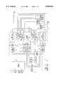
- FIG. 1is a block diagram of a conventional memory device that may use an embodiment of a test circuit in accordance with the present invention.
- FIG. 2is a block diagram of a portion of the memory device of FIG. 1 without a test circuit in accordance with the present invention.
- FIG. 3is a block diagram of a portion of the memory device of FIG. 1 using an embodiment of a test circuit in accordance with the present invention.
- FIG. 4is a block diagram of the memory device of FIGS. 1 and 3 used with a test system to determine whether the memory device is operating properly.
- FIG. 5is a block diagram of a computer system using the memory device of FIGS. 1 and 3.
- FIG. 1An embodiment of a memory device that can advantageously use an embodiment of a test circuit in accordance with the present invention is illustrated in FIG. 1.
- the memory device shown in FIG. 1is a synchronous dynamic random access memory ("SDRAM") 10, although the test circuit may also be used in other DRAM's and other memory devices.
- SDRAM 10includes an address register 12 that receives either a row address or a column address on an address bus 14.
- the address bus 14is generally coupled to a memory controller (not shown in FIG. 1).
- a row addressis initially received by the address register 12 and applied to a row address multiplexer 18.
- the row address multiplexer 18couples the row address to a number of components associated with either of two memory banks 20, 22 depending upon the state of a bank address bit forming part of the row address.
- each of the memory banks 20, 22is a respective row address latch 26 which stores the row address, and a row decoder 28 which applies various signals to its respective array 20 or 22 as a function of the stored row address.
- the row address multiplexer 18also couples row addresses to the row address latches 26 for the purpose of refreshing the memory cells in the arrays 20, 22.
- the row addressesare generated for refresh purposes by a refresh counter 30 which is controlled by a refresh controller 32.
- a column addressis applied to the address register 12.
- the address register 12couples the column address to a column address latch 40.
- the column addressis either coupled through a burst counter 42 to a column address buffer 44, or to the burst counter 42 which applies a sequence of column addresses to the column address buffer 44 starting at the column address output by the address register 12.
- the column address buffer 44applies a column address to a column decoder 48 which applies various column signals to respective sense amplifiers and associated column circuitry 50, 52 for the respective arrays 20, 22.
- Data to be read from one of the arrays 20, 22is coupled to the column circuitry 50, 52 for one of the arrays 20, 22, respectively.
- the datais then coupled to a data output register 56 which applies the data to a data bus 58.
- Data to be written to one of the arrays 20, 22is coupled from the data bus 58 through a data input register 60 to the column circuitry 50, 52 where it is transferred to one of the arrays 20, 22, respectively.
- a mask register 64may be used to selectively alter the flow of data into and out of the column circuitry 50, 52, such as by selectively masking data to be read from the arrays 20, 22.
- the above-described operation of the SDRAM 10is controlled by a command decoder 68 responsive to high level command signals received on a control bus 70.
- These high level command signalswhich are typically generated by a memory controller (not shown in FIG. 1), are a clock enable signal CKE*, a clock signal CLK, a chip select signal CS*, a write enable signal WE*, a row address strobe signal RAS*, and a column address strobe signal CAS*, which the "*" designating the signal as active low.
- the command decoder 68generates a sequence of command signals responsive to the high level command signals to carry out the function (e.g., a read or a write) designated by each of the high level command signals.
- These command signals, and the manner in which they accomplish their respective functions,are conventional. Therefore, in the interest of brevity, a further explanation of these control signals will be omitted.
- the column circuitry 50, 52 for each of the memory arrays 20, 22typically includes a sense amplifier 80, 82 for each column in each array 20, 22, respectively.
- the sense amplifiers 80, 82receive signals and apply signals to a pair of complimentary digit lines 90, 92 and 94, 96.
- the digit line 90will be at a logic "1”
- the complimentary digit line 92will be at logic "0.”
- each sense amplifier 80, 82is provided for each array 20, 22, respectively.
- the digit lines 90, 92 and 94, 96 of each sense amplifier 80, 82are selectively applied to complimentary I/O lines 100, 102 and 104, 106 by column addressing circuitry which is not shown in FIG. 2 for purposes of brevity. There is one pair of I/O lines 100, 102 and 104, 106 for each array 20, 22, respectively.
- the digit lines 90, 92are coupled to the I/O lines 100, 102, respectively, by the column addressing circuitry in the column circuitry 50 (FIG. 1).
- the digit lines 94, 96are coupled to the complimentary I/O lines 104, 106, respectively, by the column addressing circuitry in the column circuitry 52 (FIG. 1).
- the I/O lines 100-106are selectively coupled to a pair of complimentary data lines 110, 112 by a multiplexer 120 formed by pass gates 122, 124, 126, 128.
- the pass gates 122, 124are controlled by the bank address bit BA either directly or through respective inverters 130.
- the pass gates 126, 128are controlled by the inverse of the bank address signal BA at the output of an inverter 132 either directly or through inverters 134.
- BAis high, the output of the inverter 132 is low to turn on the pass gates 126, 128.
- BAis high, the I/O lines 100, 102 for the array 20 are coupled to the data lines 110, 112.
- the pass gates 122, 124are turned on to couple the I/O lines 104, 106 for the array 22 to the data lines 110, 112.
- the data lines 110, 112are, in turn, coupled to the inputs of a sense amplifier 140 having complimentary output terminals 142, 144 that are normally coupled to or part of the data output register 56 (FIG. 1).
- test circuitry 150that may be used in the column circuitry 50, 52 of the SDRAM 10 of FIG. 1 is illustrated in FIG. 3.
- An advantage of the test circuitry 150 illustrated in FIG. 3is that it utilizes many of the components that are already present in the SDRAM 10 as shown in FIG. 2. Thus, for purposes of clarity and brevity, these components in FIG. 3 have been provided with the same reference numeral, and a detailed explanation of their operation will not be repeated.
- the test circuit 150uses a switching circuit 160 or a multiplexer to control the pass gates 122-128 from either the bank address BA bit or a comparison signal COMP produced as explained above.
- the switching circuit 160is implemented using a plurality of pass gates 162, 164, 166, 168, 170, 172, 174, 176.
- the pass gates 166, 168route the bank address BA bit to the pass gates 122, 124 in the same manner as described above in FIG. 2.
- the pass gates 170, 172are enabled, they route the inverse of the bank address BA bit at the output of the inverter 132 to the pass gates 126, 128 as described above with reference to FIG. 2.
- the pass gates 166-172are controlled by a MODE* signal generated at the output of a test mode decoder 180 which is described further below.
- the active low MODE* signal and its complement at the output of an inverter 182enable the pass gates 166-172.
- the MODE* signalalso controls the conductive states of the pass gates 162, 164, 174, 176.
- An inactive high MODE* signal and its complement at the output of the inverter 182enables the pass gates 162, 164 and 174, 176.
- the pass gates 122-128are controlled by the COMP signal.
- a low COMP signalis coupled through the pass gates 162, 176 to turn on the pass gates 122, 128.
- the pass gates 122, 128then couple the digit line 90 from the array 20 and the digit line 96 from the array 22 to the inputs of the sense amplifier 140 through the I/O lines 100, 106, respectively.
- COMPwhen COMP is low, the non-complimentary digit line 90 from the array 20 and the complimentary digit line 96 from the array 22 are coupled to the sense amplifier 140.
- the MODE* and COMP signalsare generated by a conventional test mode decoder 180.
- the test mode decoder 180includes conventional decoder circuitry having inputs 190 that are coupled to externally accessible terminals of the SDRAM 10. In response to combinations of input signals that are not provided during normal operation, the test mode decoder 180 generates the desired MODE* and COMP signals.
- test circuitry 150 shown in FIG. 3couples complimentary and non-complimentary digit lines of different arrays 20, 22 to the sense amplifier 140
- the test circuitry 150could couple digit lines of different columns in the same memory array to the inputs of the sense amplifier 140.
- the test circuitry 150 shown in FIG. 3couples complimentary and non-complimentary digit lines to the sense amplifier 140, it could also be adapted to couple complimentary digit lines of different columns in the same or different arrays to the sense amplifier 140 such as, for example, coupling the I/O line 100 and the I/O line 104 to the sense amplifier 140. Regardless of which combination is used, the only requirement is that a digit line of two different columns are coupled to respective inputs of the sense amplifier 140.
- the SDRAM 10is tested using the test circuitry 150 of FIG. 3 by first writing known data to the memory arrays 20, 22 by conventional means.
- the datamay be written by addressing individual memory cells or by using conventional approaches for writing data to the memory arrays 20, 22 for test purposes, as explained above.
- a logic "1”may be written to each memory cell in the arrays 20, 22 so that when the data are read, the non-complimentary digit lines 90, 94 will be logic “1” and the complimentary digit lines 92, 96 will be logic “0.”
- logic "0”may be written to all memory cells in the arrays 20, 22 or data in some other pattern, such as a checkerboard pattern, may be written to the arrays 20, 22. In any case, as long as the data are written to the arrays 20, 22 in a known pattern, the compressed data applied to the sense amplifier 140 can provide an indication of whether the memory cells in the arrays 20, 22 are operating properly.
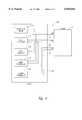
- a testing system 200 for testing the SDRAM 10 containing the test circuit 150 of FIG. 3is shown in FIG. 4.
- the SDRAM 10is connected through its address bus 14, data bus 58, and control bus 70 to a tester 260 that includes an addressing circuit 212 connected to the address bus 14, a data generator 214 connected to the data bus 58, a data analyzer 216 also connected to the data bus 58, a mode controller 218 connected to a plurality of externally accessible terminals of the SDRAM 10 in one or more of the buses 14, 58, 70, and a memory controller 220 providing central signals to the SDRAM 10 on the control bus 70.
- the data generator 214applies predetermined data to the data bus 58 while the addressing circuit 212 applies suitable addresses to the address bus 14 to cause the data on the bus 58 to be written into the SDRAM 10 under control of the memory controller 220.
- the mode controller 218generates and applies combinations of signals to the external terminals of the SDRAM 10 to cause the test mode decoder 180 to generate the MODE* and COMP signals as desired.
- the mode controller 218After known data has been written to the memory arrays 20, 22, the mode controller 218 generates a combination of signals to cause the test mode decoder 180 to drive MODE* high thereby placing the test circuitry 150 in the test mode.
- the addressing circuitry 212then addresses the memory cells of the arrays 20, 22 under control of the memory controller 220 to apply compressed data to the sense amplifier 140.
- the resulting data signals at the output terminals 142, 144 of the sense amplifier 140are coupled through the data bus 58 to the data analyzer 216.
- the data analyzer 216determines whether the data read from the SDRAM 10 corresponds to the data that was written to the SDRAM 10.
- the addressing circuits 212, data generator 214, data analyzer 216, mode controller 218, and memory controller 220can be implemented by a variety of means with relative ease by one skilled in the art.
- these componentscan be implemented in software executed by a computer system.
- the addressing circuit 212can be implemented by a counter that outputs incrementally increasing addresses
- the data generator 214can be implemented by a set of pull-up resistors that simply hold the lines of the data bus 58 at logic "1,"
- the data analyzer 216can be implemented by a latch that detects a predetermined logic level
- the mode controller 218can be implemented by a logic circuit that generates predetermined combinations of signals
- the memory controller 220can be implemented by a conventional memory controller.
- the tester 260 and its internal componentsare preferably controlled by a conventional computer system (not shown).
- FIG. 5is a block diagram of a computer system 300 which includes the SDRAM 10 of FIGS. 1 and 3.
- the computer system 300includes a processor 302 for performing various computing functions, such as executing specific software to perform specific calculations or tasks.
- the processor 302includes a processor bus 304 that normally includes an address bus, a control bus, and a data bus.
- the computer system 300includes one or more input devices 314, such as a keyboard or a mouse, coupled to the processor 302 to allow an operator to interface with the computer system 300.
- the computer system 300also includes one or more output devices 316 coupled to the processor 302, such output devices typically being a printer or a video terminal.
- One or more data storage devices 318are also typically coupled to the processor 302 to allow the processor 302 to store data or retrieve data from internal or external storage media (not shown). Examples of typical storage devices 318 include hard and floppy disks, tape cassettes, and compact disk read-only memories (CD-ROMs).
- the processor 302is also typically coupled to cache memory 326, which is usually static random access memory ("SRAM") and to the SDRAM 10 through a memory controller 330.
- the memory controller 330normally includes the control bus 70 and the address bus 14 that is coupled to the SDRAM 10.
- the data bus 58may be coupled to the processor bus 304 either directly (as shown), through the memory controller 330, or by some other means.
Landscapes
- For Increasing The Reliability Of Semiconductor Memories (AREA)
- Dram (AREA)
Abstract
Description
Claims (40)
Priority Applications (1)
| Application Number | Priority Date | Filing Date | Title |
|---|---|---|---|
| US09/133,919US6055654A (en) | 1997-07-24 | 1998-08-13 | Method and apparatus for reading compressed test data from memory devices |
Applications Claiming Priority (2)
| Application Number | Priority Date | Filing Date | Title |
|---|---|---|---|
| US08/899,525US5809038A (en) | 1997-07-24 | 1997-07-24 | Method and apparatus for reading compressed test data from memory devices |
| US09/133,919US6055654A (en) | 1997-07-24 | 1998-08-13 | Method and apparatus for reading compressed test data from memory devices |
Related Parent Applications (1)
| Application Number | Title | Priority Date | Filing Date |
|---|---|---|---|
| US08/899,525ContinuationUS5809038A (en) | 1997-07-24 | 1997-07-24 | Method and apparatus for reading compressed test data from memory devices |
Publications (1)
| Publication Number | Publication Date |
|---|---|
| US6055654Atrue US6055654A (en) | 2000-04-25 |
Family
ID=25411141
Family Applications (2)
| Application Number | Title | Priority Date | Filing Date |
|---|---|---|---|
| US08/899,525Expired - LifetimeUS5809038A (en) | 1997-07-24 | 1997-07-24 | Method and apparatus for reading compressed test data from memory devices |
| US09/133,919Expired - LifetimeUS6055654A (en) | 1997-07-24 | 1998-08-13 | Method and apparatus for reading compressed test data from memory devices |
Family Applications Before (1)
| Application Number | Title | Priority Date | Filing Date |
|---|---|---|---|
| US08/899,525Expired - LifetimeUS5809038A (en) | 1997-07-24 | 1997-07-24 | Method and apparatus for reading compressed test data from memory devices |
Country Status (3)
| Country | Link |
|---|---|
| US (2) | US5809038A (en) |
| AU (1) | AU8512298A (en) |
| WO (1) | WO1999005682A1 (en) |
Cited By (4)
| Publication number | Priority date | Publication date | Assignee | Title |
|---|---|---|---|---|
| US6295618B1 (en) | 1998-08-25 | 2001-09-25 | Micron Technology, Inc. | Method and apparatus for data compression in memory devices |
| US6483762B1 (en) | 2001-05-30 | 2002-11-19 | Micron Technology, Inc. | tRCD margin |
| US20070109887A1 (en)* | 2005-11-14 | 2007-05-17 | Ronald Baker | Memory device that provides test results to multiple output pads |
| US20080005630A1 (en)* | 2006-06-30 | 2008-01-03 | Micron Technology, Inc. | Memory device testing system and method using compressed fail data |
Families Citing this family (15)
| Publication number | Priority date | Publication date | Assignee | Title |
|---|---|---|---|---|
| US6032274A (en)* | 1997-06-20 | 2000-02-29 | Micron Technology, Inc. | Method and apparatus for compressed data testing of more than one memory array |
| US5935263A (en)* | 1997-07-01 | 1999-08-10 | Micron Technology, Inc. | Method and apparatus for memory array compressed data testing |
| US5959921A (en)* | 1997-07-24 | 1999-09-28 | Micron Technology, Inc. | Sense amplifier for complement or no-complementary data signals |
| US5995426A (en)* | 1997-11-04 | 1999-11-30 | Micron Technology, Inc. | Testing parameters of an electronic device |
| US6247088B1 (en)* | 1998-05-08 | 2001-06-12 | Lexmark International, Inc. | Bridgeless embedded PCI computer system using syncronous dynamic ram architecture |
| US6976195B1 (en)* | 1999-01-29 | 2005-12-13 | Micron Technology, Inc. | Method and apparatus for testing a memory device with compressed data using a single output |
| US6272062B1 (en)* | 2000-05-31 | 2001-08-07 | Infineon Technologies Ag | Semiconductor memory with programmable bitline multiplexers |
| JP2003223798A (en)* | 2002-01-25 | 2003-08-08 | Mitsubishi Electric Corp | Test facilitation circuit |
| US6967348B2 (en)* | 2002-06-20 | 2005-11-22 | Micron Technology, Inc. | Signal sharing circuit with microelectric die isolation features |
| US7026646B2 (en)* | 2002-06-20 | 2006-04-11 | Micron Technology, Inc. | Isolation circuit |
| US7093062B2 (en)* | 2003-04-10 | 2006-08-15 | Micron Technology, Inc. | Flash memory data bus for synchronous burst read page |
| US9003246B2 (en)* | 2012-09-29 | 2015-04-07 | Intel Corporation | Functional memory array testing with a transaction-level test engine |
| US8996934B2 (en)* | 2012-09-29 | 2015-03-31 | Intel Corporation | Transaction-level testing of memory I/O and memory device |
| US9009540B2 (en) | 2012-12-05 | 2015-04-14 | Intel Corporation | Memory subsystem command bus stress testing |
| US9009531B2 (en) | 2012-12-05 | 2015-04-14 | Intel Corporation | Memory subsystem data bus stress testing |
Citations (13)
| Publication number | Priority date | Publication date | Assignee | Title |
|---|---|---|---|---|
| EP0283906A1 (en)* | 1987-03-16 | 1988-09-28 | Siemens Aktiengesellschaft | Method and circuit arrangement for testing a semiconductor memory |
| US5029330A (en)* | 1988-06-14 | 1991-07-02 | Hitachi, Ltd. | Semiconductor memory device |
| US5268639A (en)* | 1992-06-05 | 1993-12-07 | Rambus, Inc. | Testing timing parameters of high speed integrated circuit devices |
| US5289415A (en)* | 1992-04-17 | 1994-02-22 | Motorola, Inc. | Sense amplifier and latching circuit for an SRAM |
| US5305272A (en)* | 1989-09-28 | 1994-04-19 | Kabushiki Kaisha Toshiba | Sense amplifier circuit |
| US5451898A (en)* | 1993-11-12 | 1995-09-19 | Rambus, Inc. | Bias circuit and differential amplifier having stabilized output swing |
| US5488321A (en)* | 1993-04-07 | 1996-01-30 | Rambus, Inc. | Static high speed comparator |
| US5519661A (en)* | 1993-08-10 | 1996-05-21 | Oki Electric Industry Co., Ltd. | Semiconductor memory circuit with bit line detector controlling access to data bus lines |
| US5621340A (en)* | 1995-08-02 | 1997-04-15 | Rambus Inc. | Differential comparator for amplifying small swing signals to a full swing output |
| US5684750A (en)* | 1996-03-29 | 1997-11-04 | Mitsubishi Denki Kabushiki Kaisha | Semiconductor memory device with a sense amplifier including two types of amplifiers |
| US5708607A (en)* | 1995-12-05 | 1998-01-13 | Lg Semicon Co., Ltd. | Data read circuit of a memory |
| EP0828252A2 (en)* | 1996-08-23 | 1998-03-11 | Motorola, Inc. | An integrated circuit for configuring modes in a memory |
| EP0840328A2 (en)* | 1996-10-31 | 1998-05-06 | Texas Instruments Incorporated | Method and device for testing memory circuits |
Family Cites Families (2)
| Publication number | Priority date | Publication date | Assignee | Title |
|---|---|---|---|---|
| JPS63266692A (en)* | 1987-04-24 | 1988-11-02 | Hitachi Ltd | semiconductor storage device |
| KR0127680B1 (en)* | 1987-08-07 | 1998-04-03 | 미다 가쓰시게 | Semiconductor memory |
- 1997
- 1997-07-24USUS08/899,525patent/US5809038A/ennot_activeExpired - Lifetime
- 1998
- 1998-07-23WOPCT/US1998/015392patent/WO1999005682A1/enactiveApplication Filing
- 1998-07-23AUAU85122/98Apatent/AU8512298A/ennot_activeAbandoned
- 1998-08-13USUS09/133,919patent/US6055654A/ennot_activeExpired - Lifetime
Patent Citations (13)
| Publication number | Priority date | Publication date | Assignee | Title |
|---|---|---|---|---|
| EP0283906A1 (en)* | 1987-03-16 | 1988-09-28 | Siemens Aktiengesellschaft | Method and circuit arrangement for testing a semiconductor memory |
| US5029330A (en)* | 1988-06-14 | 1991-07-02 | Hitachi, Ltd. | Semiconductor memory device |
| US5305272A (en)* | 1989-09-28 | 1994-04-19 | Kabushiki Kaisha Toshiba | Sense amplifier circuit |
| US5289415A (en)* | 1992-04-17 | 1994-02-22 | Motorola, Inc. | Sense amplifier and latching circuit for an SRAM |
| US5268639A (en)* | 1992-06-05 | 1993-12-07 | Rambus, Inc. | Testing timing parameters of high speed integrated circuit devices |
| US5488321A (en)* | 1993-04-07 | 1996-01-30 | Rambus, Inc. | Static high speed comparator |
| US5519661A (en)* | 1993-08-10 | 1996-05-21 | Oki Electric Industry Co., Ltd. | Semiconductor memory circuit with bit line detector controlling access to data bus lines |
| US5451898A (en)* | 1993-11-12 | 1995-09-19 | Rambus, Inc. | Bias circuit and differential amplifier having stabilized output swing |
| US5621340A (en)* | 1995-08-02 | 1997-04-15 | Rambus Inc. | Differential comparator for amplifying small swing signals to a full swing output |
| US5708607A (en)* | 1995-12-05 | 1998-01-13 | Lg Semicon Co., Ltd. | Data read circuit of a memory |
| US5684750A (en)* | 1996-03-29 | 1997-11-04 | Mitsubishi Denki Kabushiki Kaisha | Semiconductor memory device with a sense amplifier including two types of amplifiers |
| EP0828252A2 (en)* | 1996-08-23 | 1998-03-11 | Motorola, Inc. | An integrated circuit for configuring modes in a memory |
| EP0840328A2 (en)* | 1996-10-31 | 1998-05-06 | Texas Instruments Incorporated | Method and device for testing memory circuits |
Non-Patent Citations (14)
| Title |
|---|
| "Draft Standard for a High-Speed Memory Interface (SyncLink)," Microprocessor and Microcomputer Standards Subcommittee of the IEEE Computer Society, Copyright 1996 by the Institute of Electrical and Electronics Engineers, Inc. New York, NY, pp. 1-56. |
| Descriptive literature entitled, "400MHz SLDRAM, 4M×16 SLDRAM Pipelined, Eight Bank, 2.5 V Operation," SLDRAM Consortium Advance Sheet, published throughout the United States, pp.1-22. |
| Descriptive literature entitled, 400MHz SLDRAM, 4M 16 SLDRAM Pipelined, Eight Bank, 2.5 V Operation, SLDRAM Consortium Advance Sheet, published throughout the United States, pp.1 22.* |
| Draft Standard for a High Speed Memory Interface (SyncLink), Microprocessor and Microcomputer Standards Subcommittee of the IEEE Computer Society, Copyright 1996 by the Institute of Electrical and Electronics Engineers, Inc. New York, NY, pp. 1 56.* |
| Ishibashi, K. et al, "A 6-ns 4-Mb CMOS SRAM with Offset-Voltage-Insensitive Current Sense Amplifiers," IEEE Journal of Solid-State Circuits, vol. 30, No. 4, Apr. 1995, pp. 728-733. |
| Ishibashi, K. et al, A 6 ns 4 Mb CMOS SRAM with Offset Voltage Insensitive Current Sense Amplifiers, IEEE Journal of Solid State Circuits, vol. 30, No. 4, Apr. 1995, pp. 728 733.* |
| Kuroda, T. et al., "Automated Bias Control (ABC) Circuit for High-Performance VLSI's," IEEE Journal of Solid-State Circuits, vol. 27, No. 4, Apr. 1992, pp. 539-545. |
| Kuroda, T. et al., Automated Bias Control (ABC) Circuit for High Performance VLSI s, IEEE Journal of Solid State Circuits, vol. 27, No. 4, Apr. 1992, pp. 539 545.* |
| Taguchi M. et al., A 40ns 64Mb DRAM with Current Sensing Data Bus Amplifier, ISSCC Digest of Technical Papers, 1991, TAM 6.5.* |
| Taguchi M. et al., A 40ns 64Mb DRAM with Current-Sensing Data-Bus Amplifier, ISSCC Digest of Technical Papers, 1991, TAM 6.5. |
| Taguchi, M. et al., "A 40-ns 64-Mb DRAM with 64-b Parallel Data Bus Architecture," IEEE Journal of Solid-State Circuits, vol. 26, No. 11, Nov. 1991, pp. 1493-1497. |
| Taguchi, M. et al., A 40 ns 64 Mb DRAM with 64 b Parallel Data Bus Architecture, IEEE Journal of Solid State Circuits, vol. 26, No. 11, Nov. 1991, pp. 1493 1497.* |
| Takeshi, N. et al., "A 17-ns 4-Mb CMOS DRAM," IEEE Journal of Solid State Circuits, vol. 26, No. 11, Nov. 1991, pp. 1538-1543. |
| Takeshi, N. et al., A 17 ns 4 Mb CMOS DRAM, IEEE Journal of Solid State Circuits, vol. 26, No. 11, Nov. 1991, pp. 1538 1543.* |
Cited By (24)
| Publication number | Priority date | Publication date | Assignee | Title |
|---|---|---|---|---|
| US20040240285A1 (en)* | 1998-08-25 | 2004-12-02 | Brent Keeth | Method and apparatus for data compression in memory devices |
| US7190625B2 (en) | 1998-08-25 | 2007-03-13 | Micron Technology, Inc. | Method and apparatus for data compression in memory devices |
| US7136316B2 (en) | 1998-08-25 | 2006-11-14 | Micron Technology, Inc. | Method and apparatus for data compression in memory devices |
| US6999361B2 (en) | 1998-08-25 | 2006-02-14 | Micron Technology, Inc. | Method and apparatus for data compression in memory devices |
| US6987702B2 (en) | 1998-08-25 | 2006-01-17 | Mycron Technology, Inc. | Method and apparatus for data compression in memory devices |
| US20050286326A1 (en)* | 1998-08-25 | 2005-12-29 | Brent Keeth | Method and apparatus for data compression in memory devices |
| US6295618B1 (en) | 1998-08-25 | 2001-09-25 | Micron Technology, Inc. | Method and apparatus for data compression in memory devices |
| US20050286325A1 (en)* | 1998-08-25 | 2005-12-29 | Brent Keeth | Method and apparatus for data compression in memory devices |
| US6819611B2 (en) | 1998-08-25 | 2004-11-16 | Micron Technology, Inc. | Method and apparatus for data compression in memory devices |
| US20040240284A1 (en)* | 1998-08-25 | 2004-12-02 | Brent Keeth | Method and apparatus for data compression in memory devices |
| US6687176B2 (en) | 2001-05-30 | 2004-02-03 | Micron Technology, Inc. | First bit databurst firing of IO equilibrating ending signal based on column access signal |
| US6493286B1 (en) | 2001-05-30 | 2002-12-10 | Micron Technology, Inc. | tRCD margin |
| US20050169080A1 (en)* | 2001-05-30 | 2005-08-04 | Micron Technology, Inc. | Triggering of IO equilibrating ending signal with firing of column access signal |
| US6693835B2 (en) | 2001-05-30 | 2004-02-17 | Micron Technology, Inc. | TRCD margin |
| US6574164B2 (en) | 2001-05-30 | 2003-06-03 | Micron Technology, Inc. | tRCD margin |
| US20030079095A1 (en)* | 2001-05-30 | 2003-04-24 | Protzman Brendan N. | Triggering of IO equilibrating ending signal with firing of column access signal |
| US6501688B2 (en) | 2001-05-30 | 2002-12-31 | Micron Technology, Inc. | tRCD margin |
| US6877064B2 (en) | 2001-05-30 | 2005-04-05 | Micron Technology, Inc. | Triggering of IO equilibrating ending signal with firing of column access signal |
| US6483762B1 (en) | 2001-05-30 | 2002-11-19 | Micron Technology, Inc. | tRCD margin |
| US7339839B2 (en) | 2001-05-30 | 2008-03-04 | Micron Technology, Inc. | Triggering of IO equilibrating ending signal with firing of column access signal |
| US20070109887A1 (en)* | 2005-11-14 | 2007-05-17 | Ronald Baker | Memory device that provides test results to multiple output pads |
| US7457170B2 (en) | 2005-11-14 | 2008-11-25 | Infineon Technologies Ag | Memory device that provides test results to multiple output pads |
| US20080005630A1 (en)* | 2006-06-30 | 2008-01-03 | Micron Technology, Inc. | Memory device testing system and method using compressed fail data |
| US7596729B2 (en) | 2006-06-30 | 2009-09-29 | Micron Technology, Inc. | Memory device testing system and method using compressed fail data |
Also Published As
| Publication number | Publication date |
|---|---|
| AU8512298A (en) | 1999-02-16 |
| WO1999005682A1 (en) | 1999-02-04 |
| US5809038A (en) | 1998-09-15 |
Similar Documents
| Publication | Publication Date | Title |
|---|---|---|
| US6055654A (en) | Method and apparatus for reading compressed test data from memory devices | |
| US6987702B2 (en) | Method and apparatus for data compression in memory devices | |
| US6536004B2 (en) | On-chip circuit and method for testing memory devices | |
| US6163863A (en) | Method and circuit for compressing test data in a memory device | |
| US6058056A (en) | Data compression circuit and method for testing memory devices | |
| US5982682A (en) | Self-test circuit for memory integrated circuits | |
| US6097644A (en) | Redundant row topology circuit, and memory device and test system using same | |
| US6751159B2 (en) | Memory device operable in either a high-power, full-page size mode or a low-power, reduced-page size mode | |
| US6459635B1 (en) | Apparatus and method for increasing test flexibility of a memory device | |
| US6483760B2 (en) | Semiconductor memory integrated circuit operating at different test modes | |
| US6691247B2 (en) | Circuit and method for masking a dormant memory cell | |
| US6314036B1 (en) | Method and apparatus for efficiently testing RAMBUS memory devices | |
| KR100474985B1 (en) | Memory Logic Semiconductor Device | |
| US5936975A (en) | Semiconductor memory device with switching circuit for controlling internal addresses in parallel test | |
| US6936889B2 (en) | Semiconductor device and method for testing semiconductor device | |
| JPH0821607B2 (en) | Dynamic storage device and burn-in method thereof | |
| US6356474B1 (en) | Efficient open-array memory device architecture and method | |
| KR20000077069A (en) | Semiconductor memory device | |
| US5986953A (en) | Input/output circuits and methods for testing integrated circuit memory devices | |
| JPH05274863A (en) | Dynamic semiconductor storage device |
Legal Events
| Date | Code | Title | Description |
|---|---|---|---|
| STCF | Information on status: patent grant | Free format text:PATENTED CASE | |
| CC | Certificate of correction | ||
| FPAY | Fee payment | Year of fee payment:4 | |
| FPAY | Fee payment | Year of fee payment:8 | |
| FPAY | Fee payment | Year of fee payment:12 | |
| AS | Assignment | Owner name:U.S. BANK NATIONAL ASSOCIATION, AS COLLATERAL AGENT, CALIFORNIA Free format text:SECURITY INTEREST;ASSIGNOR:MICRON TECHNOLOGY, INC.;REEL/FRAME:038669/0001 Effective date:20160426 Owner name:U.S. BANK NATIONAL ASSOCIATION, AS COLLATERAL AGEN Free format text:SECURITY INTEREST;ASSIGNOR:MICRON TECHNOLOGY, INC.;REEL/FRAME:038669/0001 Effective date:20160426 | |
| AS | Assignment | Owner name:MORGAN STANLEY SENIOR FUNDING, INC., AS COLLATERAL AGENT, MARYLAND Free format text:PATENT SECURITY AGREEMENT;ASSIGNOR:MICRON TECHNOLOGY, INC.;REEL/FRAME:038954/0001 Effective date:20160426 Owner name:MORGAN STANLEY SENIOR FUNDING, INC., AS COLLATERAL Free format text:PATENT SECURITY AGREEMENT;ASSIGNOR:MICRON TECHNOLOGY, INC.;REEL/FRAME:038954/0001 Effective date:20160426 | |
| AS | Assignment | Owner name:U.S. BANK NATIONAL ASSOCIATION, AS COLLATERAL AGENT, CALIFORNIA Free format text:CORRECTIVE ASSIGNMENT TO CORRECT THE REPLACE ERRONEOUSLY FILED PATENT #7358718 WITH THE CORRECT PATENT #7358178 PREVIOUSLY RECORDED ON REEL 038669 FRAME 0001. ASSIGNOR(S) HEREBY CONFIRMS THE SECURITY INTEREST;ASSIGNOR:MICRON TECHNOLOGY, INC.;REEL/FRAME:043079/0001 Effective date:20160426 Owner name:U.S. BANK NATIONAL ASSOCIATION, AS COLLATERAL AGEN Free format text:CORRECTIVE ASSIGNMENT TO CORRECT THE REPLACE ERRONEOUSLY FILED PATENT #7358718 WITH THE CORRECT PATENT #7358178 PREVIOUSLY RECORDED ON REEL 038669 FRAME 0001. ASSIGNOR(S) HEREBY CONFIRMS THE SECURITY INTEREST;ASSIGNOR:MICRON TECHNOLOGY, INC.;REEL/FRAME:043079/0001 Effective date:20160426 | |
| AS | Assignment | Owner name:MICRON TECHNOLOGY, INC., IDAHO Free format text:RELEASE BY SECURED PARTY;ASSIGNOR:U.S. BANK NATIONAL ASSOCIATION, AS COLLATERAL AGENT;REEL/FRAME:047243/0001 Effective date:20180629 | |
| AS | Assignment | Owner name:MICRON TECHNOLOGY, INC., IDAHO Free format text:RELEASE BY SECURED PARTY;ASSIGNOR:MORGAN STANLEY SENIOR FUNDING, INC., AS COLLATERAL AGENT;REEL/FRAME:050937/0001 Effective date:20190731 |