US6054647A - Grid material for electromagnetic shielding - Google Patents
Grid material for electromagnetic shieldingDownload PDFInfo
- Publication number
- US6054647A US6054647AUS08/979,190US97919097AUS6054647AUS 6054647 AUS6054647 AUS 6054647AUS 97919097 AUS97919097 AUS 97919097AUS 6054647 AUS6054647 AUS 6054647A
- Authority
- US
- United States
- Prior art keywords
- nickel
- grid
- coated
- grid material
- substrate material
- Prior art date
- Legal status (The legal status is an assumption and is not a legal conclusion. Google has not performed a legal analysis and makes no representation as to the accuracy of the status listed.)
- Expired - Fee Related
Links
Images


Classifications
- H—ELECTRICITY
- H05—ELECTRIC TECHNIQUES NOT OTHERWISE PROVIDED FOR
- H05K—PRINTED CIRCUITS; CASINGS OR CONSTRUCTIONAL DETAILS OF ELECTRIC APPARATUS; MANUFACTURE OF ASSEMBLAGES OF ELECTRICAL COMPONENTS
- H05K9/00—Screening of apparatus or components against electric or magnetic fields
- H05K9/0073—Shielding materials
- H05K9/0081—Electromagnetic shielding materials, e.g. EMI, RFI shielding
- H05K9/009—Electromagnetic shielding materials, e.g. EMI, RFI shielding comprising electro-conductive fibres, e.g. metal fibres, carbon fibres, metallised textile fibres, electro-conductive mesh, woven, non-woven mat, fleece, cross-linked
Definitions
- the present inventionrelates to a novel grid material that is capable of being joined with a plastic molding to provide a shielding structure for shielding electromagnetic waves from an electronic device.
- the grid materialis a nickel-coated mesh-like material or substrate that is annealed and calendared together to provide a bonded unitary grid structure.
- the grid materialprovides a conductor in the shielded structure and provides a flexible grid material which readily permits the insertion and placement with respect to an electrical mold cavity to permit the insert molding of the shielding housing.
- Electromagnetic interference (E.M.I.) shielding structuresexist to provide protection for an electronic instrument or device from electromagnetic energy, including radio frequency interference (R.F.I.).
- the shielding structureshopefully provide protection for the electronic device by preventing electromagnetic wave energy from penetrating the device, as well as escaping from the device.
- electromagnetic shielding productshave generally been made by the formation of sheet metal boxes; conductive paints applied to a plastic housing, die cast parts to construct a housing and filled resins containing metal fibers.
- prior art sheet metal devices for providing shielding structureshave found only limited application because of the difficulties of weight restrictions in shielding housings, the inability to make round shapes, noise problems and the requirement of multiple parts.
- Conductive paintsinclude electroplating metal onto a plastic, a technique which requires a second processing step, provides poor performance, is cost prohibitive, presents environmental problems and is susceptible to chipping and flaking. Filled resins are very expensive and destroy insert molding tooling and exhibit poor shielding properties.
- the resultant shielding housing used to enclose and shield an electronic devicerequires external connections and supplemental shielding at the joints or corners of the enclosure to provide the box-like enclosure.
- Such assembly techniquesare expensive and time consuming and oftentimes result in a structure which does not properly shield the enclosed device. Accordingly, such shielding structures and approaches have found only limited acceptance.
- such shielding structuresmay require is complex conductive junctions and connections between shielding panels, assembly techniques that are expensive and time consuming and which oftentimes result in unacceptable shielding housings.
- One object of the present inventionis to provide a novel grid material or substrate which is capable of being utilized in conjunction with an injection mold to provide the molding of box-like shielding structures or housings.
- the nickel-coated grid materialpossess sufficient strength and sufficient flexibility to permit use with an injection mold such that the resultant molding provides a shielding structure having a base and integrally molded sidewalls.
- the mesh-like grid structure of the present inventionis particularly useful in incorporation with a molded housing for shielding electromagnetic waves propagating into and exiting from various type electronic devices.
- the mesh-like grid structure or substrate materialis, preferably, prepared by electroplating and depositing a nickel coating onto a steel rod.
- the nickel-coated steel rodis then drawn to a predetermined wire size which corresponds to the desired diameter wire from which a mesh or screen is desired to be woven.
- Multiple nickel-coated drawn and sized wiresare then directed to a loom which weaves the nickel-coated wires into a wire cloth, such as a mesh or screen.
- the nickel-coated mesh or screenmay be stored for subsequent treatment or may be immediately treated by annealing in a reducing furnace between a temperature of about 1630-1680° F. so that the strands of the mesh or screen are partially fused or bonded together at each intersecting cross-over point of the annealed mesh or screen. Thereafter, the annealed and partially fused or bonded mesh or screen may be either again stored for subsequent treatment or it may be immediately treated by directing the annealed and partially bonded mesh through calendering rollers, to flatten the annealed and partially bonded material to a predetermined thickness while thereby increasing and completing the bonding between the intersecting cross-over points.
- the increased bonding resulting from the calendering operationprovides more integrity to the resultant unitary grid material or substrate and increases the conductivity of the gird substrate.
- the unitary grid material or substratemay be stored or may be immediately directed through a slitter or cutter to provide the desired dimensions of the grid material or substrate for use with a mold for making the grid shielding housings.
- the nickel-coated grid material or substrateis very compatible with plastic moldings in that the nickel-coated grid material does not oxidize when integrally molded to or adjacent the surface of the molding. Because the nickel interstices or cross-over points in the wire grid are fully and completely metallurgically bonded together, the resultant unitary grid material exhibits substantial flexibility and strength, properties which depend upon the drawn wire diameter and the nickel-coating weight of the resultant grid material. For example, the nickel coating weight with respect to the mesh or screen, may range between approximately about 1 to 20 percent depending upon the ultimate application of the grid material.
- a typical grid material of between about 14 ⁇ 14 up to 100 ⁇ 100 wires per inch and having a wire diameter of between about 0.002 to 0.015 incheshave been utilized in making the novel grid material or substrate.
- Such grid materialmay be advantageously positioned and inserted into an injection mold to provide a molded shielding housing or structure which provides excellent electromagnetic wave and radio frequency shielding properties.
- the flexibility of the grid materialis determined by the dimension and number of wires per inch in the grid material, as well as by the degree of flattening achieved during calendering of the annealed material.
- the calendering processreduces the thickness or width of the annealed grid material from between about 20 to 30 percent. This compaction or flattening, it is believed, increases the strength of the grid material or substrate by increasing the bond between the cross-over points in the grid material or substrate.
- the novel grid material or substratehas particular application as a shielding product when molded in an injection mold.
- the subsequent molding of the grid substrate to a housingprovides a molded shielded housing particularly useful in preventing electromagnetic waves from penetrating into the housing or escaping from the housing.
- FIG. 1is a schematic view showing the step of electroplating nickel onto a steel rod to provide a coated rod stock and drawing the coated rod stock through a die to provide a proper filament or wire size of the nickel-coated wire in accordance with the present invention
- FIG. 2is a schematic view illustrating the steps of weaving a mesh or screen material from the nickel-coated drawn wire in accordance with the present invention
- FIG. 2Ais an enlarged view of the mesh or screen material obtained during weaving of the nickel-coated drawn wires in accordance with the present invention
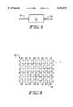
- FIG. 3is a schematic view showing the step of directing the nickel-coated mesh or screen material into and through a reducing furnace for annealing the nickel-coated mesh or screen so that the wires of the mesh or screen are partially fused or bonded together at each intersecting cross-over point to provide a partially bonded and annealed grid material in accordance with the present invention
- FIG. 4is a schematic view showing the step of calendering is the partially fused and annealed grid material to increase the bond at each intersecting cross-over point to provide the grid material or substrate in accordance with the present invention
- FIG. 5is a schematic view showing the step of running the calendared grid material or substrate through a slitter or cutter to provide the desired grid material width and dimension in accordance with the present invention
- FIG. 6is an enlarged schematic top plan view of the novel nickel coated grid material or substrate in accordance with the present invention.
- FIGS. 7-10are schematic views of various types of electronic devices enclosed within a molded shielding housing utilizing the novel grid material in accordance with the present invention.
- the present inventionis directed to a mesh-like grid structure or substrate 10, as shown in FIG. 6, and the method of making the grid substrate, as shown in FIGS. 1-5.
- the mesh-like grid structure 10is prepared by electroplating a nickel coating onto a steel rod 13, as shown in FIG. 1.
- the electroplating solution 15is comprised of nickel fluoroborate. The time and conditions for the electroplating step determines the amount of nickel coating deposited on the steel rod 13.
- the nickel-coated steel rod 12 exiting the electroplating bathis then drawn through a die 14 to a desired or predetermined wire diameter to provide a nickel-coated wire 12a.
- the range in wire diameter of the drawn nickel-coated wire 12ais between about 0.002 to 0.015 inches, with between about 0.004 to 0.0075 inches being preferred.
- a plurality of the nickel-coated wires 12aare then directed to a loom station 16 which weaves the coated wires 12 into a wire cloth, such as a coated mesh or screen 17, as shown in FIG. 2A.
- the nickel-coated mesh or screen 17may be stored for subsequent treatment or it may be immediately directed through an annealing furnace under a reducing atmosphere, such as hydrogen, to raise the temperature of the nickel-coated mesh or screen to a temperature between about 1630° F. to 1680° F.
- the wires in the nickel-coated mesh or screen material 17are annealed and partially fused or bonded together at each intersecting cross-over point 18 of the nickel-coated screen material 17.
- the partially welded or bonded mesh or screen material 17may be either stored for subsequent treatment or may be immediately treated by directing the partially bonded and annealed mesh or screen material 17 through a pair of calendering rollers 20 (FIG. 4) in a calendering station 21 to flatten the annealed and partially bonded mesh or screen material 17 to a predetermined thickness.
- the step of calenderingprovides a desired thickness to the final grid material or substrate 10 and increases the strength of the bonding that is provided by the nickel coating 12 between the intersecting cross-over points 18.
- the grid material exiting the calendering rollersmay be either placed in storage for subsequent usage or may be immediately directed through a slitter or cutter 22, to provide the desired dimensions and size for the grid material or substrate 10.
- the nickel-coated grid material or substrate 10 in accordance with the present inventionis shown wherein each of the cross-over points 18 is fully bonded to one another by the nickel coating.
- the partially fused or bonded annealed grid material 17 entering the calendering station 21is subjected to a compaction between calendering rollers 20 which reduces the thickness or flattens the annealed partially bonded grid structure 17 to increase the bond at the cross-over points and to reduce the thickness of the annealed grid material by approximately 20 to 30 percent.
- a 0.006 inch thick partially bonded grid structurewill be compacted to about a thickness of 0.0045 inches.
- the mesh-like grid structure or substrate 10 in accordance with the present inventionis particularly useful for incorporation with molded housings for shielding electromagnetic waves entering or exiting from various electronic devices. It has been found that the nickel-coated grid material 10 is very compatible with plastic molding in that the nickel-coated grid material does not readily oxidize when it is near or on the surface of the molding.
- the grid substrate 10may be positioned on the surface of the molding, within the molding or a combination of both. It is only necessary that the grid substrate be integral with the molded housing.
- Such a shielding structure or housing 24(FIGS. 7-10) provides excellent anti-corrosive properties and provides excellent electrical contact and sealing when assembled into box-like shielding devices.
- the nickel-coated interstices and cross-over points 18 of the grid structure 10are fully bonded together, a structure and condition which provides uniform electrical contacts within the shielding housing.
- the percent of nickel in the coating with respect to the total weight of the grid materialmay range from between about 1 to 20 percent, depending upon the desired application of the grid material.
- a typical grid material of between about 14 ⁇ 14 up to 100 ⁇ 100 wires per inch and having a wire diameter of between about 0.002 to 0.015 incheshave been utilized in making the novel grid material or substitute and may be advantageously positioned within an injection mold to provide a molded shielded housing or structure 24.
- the flexibility of the grid material 10is determined by the size and number of coated wires in the annealed nickel-coated screen or mesh 17 as well as by the degree of flattening attained during calendering of the annealed material 17. It is preferred that approximately a 20 to 30 percent reduction in thickness between the annealed partially bonded material 17 and the final calendared bonded grid material or substrate 10 is desired in accordance with the present invention.
- the compaction or flattening of the materialincreases the strength of the grid material and increases the bonding between the cross-over points 18 of the grid material 10.
- the nickel coating of the present inventionis desirable as a shielding material because nickel sinters and bonds well at a relatively lower temperature, the nickel coating in the ultimate molded plastic part is compatible with the injectable plastic, the nickel coating tends not to oxidize when it is positioned or exposed on the surface of the molded plastic housing and the nickel coating enhances the bonding of the grid matrix at the cross-over points of the grid structure.
- the grid material or substrate in accordance with the present inventionhas particular application as a shielding product when it is incorporated as part of a molded shielding housing 24.
- the diameter of the drawn wires 12a directed into the weaving machine stationmay vary in diameter from about 0.002 to 0.015 inches. The smaller the wire diameter, the greater the flexibility of the resultant grid material.
- the use of the novel grid structure in conjunction with molded housingsprovides excellent shielding structures that are lightweight and durable.
- the novel molded shielding containers or housings 24may include box-like structures that enclose radios and CD players 30 (FIG. 7), electronic control units 31, such as airbag control modules, engine control modules, dashboard electronic modules, electronic control units within a vehicle, and industrial control modules (FIG. 8), automotive motors 32, such as windshield wiper motors, window regulation motors and seat adjustment motors (FIG. 9) and electronic devices 33 (FIG. 10), such as computers, printers, cable boxes, disk drive cases, computer screens and monitors, photocopier subassemblies, data transmission equipment, cellular phones and portable electronic medical units.
- radios and CD players 30FIG. 7
- electronic control units 31such as airbag control modules, engine control modules, dashboard electronic modules, electronic control units within a vehicle, and industrial control modules (FIG. 8)
- automotive motors 32such as windshield wiper motors, window regulation motors and seat adjustment motors (FIG. 9)
- electronic devices 33FIG. 10
Landscapes
- Engineering & Computer Science (AREA)
- Textile Engineering (AREA)
- Physics & Mathematics (AREA)
- Electromagnetism (AREA)
- Microelectronics & Electronic Packaging (AREA)
- Shielding Devices Or Components To Electric Or Magnetic Fields (AREA)
Abstract
Description
Claims (7)
Priority Applications (1)
| Application Number | Priority Date | Filing Date | Title |
|---|---|---|---|
| US08/979,190US6054647A (en) | 1997-11-26 | 1997-11-26 | Grid material for electromagnetic shielding |
Applications Claiming Priority (1)
| Application Number | Priority Date | Filing Date | Title |
|---|---|---|---|
| US08/979,190US6054647A (en) | 1997-11-26 | 1997-11-26 | Grid material for electromagnetic shielding |
Publications (1)
| Publication Number | Publication Date |
|---|---|
| US6054647Atrue US6054647A (en) | 2000-04-25 |
Family
ID=25526769
Family Applications (1)
| Application Number | Title | Priority Date | Filing Date |
|---|---|---|---|
| US08/979,190Expired - Fee RelatedUS6054647A (en) | 1997-11-26 | 1997-11-26 | Grid material for electromagnetic shielding |
Country Status (1)
| Country | Link |
|---|---|
| US (1) | US6054647A (en) |
Cited By (34)
| Publication number | Priority date | Publication date | Assignee | Title |
|---|---|---|---|---|
| US6405014B2 (en)* | 1999-12-28 | 2002-06-11 | Toshiba Tec Kabushiki Kaisha | Fixing device for fixing a developer image on a recording medium by induction-heating a heat roller |
| US20020166682A1 (en)* | 2001-05-10 | 2002-11-14 | Watchko George R. | Manufacture of electronics enclosure having a metallized shielding layer |
| US6610395B2 (en) | 2001-06-11 | 2003-08-26 | Honeywell International Inc. | Breathable electromagnetic shielding material |
| US6697248B1 (en) | 2001-02-06 | 2004-02-24 | Daniel Luch | Electromagnetic interference shields and methods of manufacture |
| US6706092B2 (en) | 2002-04-17 | 2004-03-16 | Alliedsignal Inc. | Chemical/Biological decontamination filter |
| US20040119201A1 (en)* | 2002-07-12 | 2004-06-24 | Siegel-Robert, Inc. | Apparatus and method for manufacturing plastic products with EMI/RFI/ESD shield |
| US20050029919A1 (en)* | 2003-06-26 | 2005-02-10 | Matsushita Electric Industrial Co., Ltd. | Electromagnetic wave shield |
| US6855883B1 (en)* | 1997-02-11 | 2005-02-15 | Kazu Investment Co., Ltd. | Electromagnetic wave blocking material and electromagnetic wave blocking case |
| US20050036279A1 (en)* | 2003-08-17 | 2005-02-17 | Ko-Chen Tan | Electronic apparatus with a housing for seeing inside |
| US20050057422A1 (en)* | 2003-09-01 | 2005-03-17 | Matsushita Electric Industrial Co., Ltd. | Gate antenna device |
| US20050129914A1 (en)* | 2003-11-20 | 2005-06-16 | Rim Peter B. | Protective fabrics |
| US20050140564A1 (en)* | 2003-10-29 | 2005-06-30 | Matsushita Electric Industrial Co., Ltd. | Loop antenna |
| US20050244608A1 (en)* | 2002-08-08 | 2005-11-03 | Dai Nippon Printing Co., Ltd. | Electromagnetic wave shielding sheet |
| US20060196692A1 (en)* | 2005-03-01 | 2006-09-07 | Fujitsu Limited | Vent grid and electronic apparatus employing the same |
| US7176387B1 (en)* | 2005-12-05 | 2007-02-13 | King Star Enterprise, Inc. | Electromagnetic shielding device |
| US20070084631A1 (en)* | 2005-05-17 | 2007-04-19 | Wolfgang Kessel | Electromagnetic shielding |
| US20080049949A1 (en)* | 2006-08-18 | 2008-02-28 | Snider Chris R | Lightweight audio system for automotive applications and method |
| EP1927419A1 (en)* | 2006-12-03 | 2008-06-04 | Waldemar Hoening oHG | Grid comprising netted wires having a thick tinning |
| USD571608S1 (en)* | 2006-10-05 | 2008-06-24 | Sar Holdings International Limited | Heat insulation holder |
| US20090051258A1 (en)* | 2007-08-24 | 2009-02-26 | Samsung Corning Precision Glass Co., Ltd. | Electromagnetic wave blocking member for display apparatus |
| EP2153984A1 (en)* | 2002-12-27 | 2010-02-17 | Toray Industries, Inc. | Layered product, electromagnetic-shielding molded object, and processes for producing these |
| US20100190111A1 (en)* | 2007-03-30 | 2010-07-29 | Fujifilm Corporation | Conductive film and method for producing the same |
| US20100282505A1 (en)* | 2005-09-30 | 2010-11-11 | Fujifilm Corporation | Method for producing conductive film and light-sensitive material for conductive film production |
| CN101888770A (en)* | 2010-07-07 | 2010-11-17 | 中兴通讯股份有限公司 | Flexible conducting material substrate and implementing method thereof |
| DE102010013486A1 (en)* | 2010-03-30 | 2011-10-06 | Waldemar Hoening Ohg | Soldered electrode for electric actuator, has stripy solder layer arranged to stripy formed net electrode part, where stripy solder layer and/or net electrode part is folded to connect stripy solder layer with net electrode |
| US20120037420A1 (en)* | 2010-08-16 | 2012-02-16 | The Boeing Company | Electronic device protection |
| US8760886B2 (en) | 2006-08-18 | 2014-06-24 | Delphi Technologies, Inc. | Lightweight audio system for automotive applications and method |
| US8947892B1 (en) | 2010-08-16 | 2015-02-03 | The Boeing Company | Electronic device protection |
| US9237685B2 (en) | 2006-08-18 | 2016-01-12 | Delphi Technologies, Inc. | Lightweight audio system for automotive applications and method |
| US9324472B2 (en) | 2010-12-29 | 2016-04-26 | Syscom Advanced Materials, Inc. | Metal and metallized fiber hybrid wire |
| US20180295756A1 (en)* | 2017-04-07 | 2018-10-11 | Fujitsu Limited | Electromagnetic wave absorber and electronic device |
| US20210137327A1 (en)* | 2019-11-13 | 2021-05-13 | Emerson Electric Co. | Vacuum cleaner motor assemblies and methods of operating same |
| CN116008713A (en)* | 2023-02-22 | 2023-04-25 | 中国人民解放军陆军工程大学 | An electromagnetic interference detection system for UAV flight control system |
| US20240412024A1 (en)* | 2023-06-07 | 2024-12-12 | Toshiba Global Commerce Solutions, Inc. | Selective radio frequency identification shielding |
Citations (46)
| Publication number | Priority date | Publication date | Assignee | Title |
|---|---|---|---|---|
| US2585054A (en)* | 1949-03-10 | 1952-02-12 | Edward J Stachura | Flexible shield for electric conductors |
| US3150792A (en)* | 1958-05-01 | 1964-09-29 | Air Logistics Corp | Reinforced plastic molded article and method of making same |
| US3426940A (en)* | 1966-11-21 | 1969-02-11 | Phillips Petroleum Co | Pressure vessels |
| US3931908A (en)* | 1973-08-02 | 1976-01-13 | Kaiser Aluminum & Chemical Corporation | Insulated tank |
| US4017967A (en)* | 1975-03-31 | 1977-04-19 | Black Body Corporation | Method of making infrared emitter |
| US4215796A (en)* | 1979-05-10 | 1980-08-05 | General Electric Company | Radio frequency shield structure |
| US4505658A (en)* | 1983-04-06 | 1985-03-19 | Maschinenfabrik Ettlingen Friedrich Pfeiffer Kg | Mechanism for centering reinforcing mesh |
| JPS60177699A (en)* | 1984-02-24 | 1985-09-11 | 昭和電工株式会社 | Method of producing electromagnetic wave shielding housing |
| US4593736A (en)* | 1985-01-09 | 1986-06-10 | Tamao Morita | Case or bag covered with a magnet shielding material |
| US4631214A (en)* | 1984-12-24 | 1986-12-23 | Fukuvi Chemical Industry Co., Ltd. | Transparent electromagnetic wave shielding material |
| JPS6262719A (en)* | 1985-09-12 | 1987-03-19 | Mitsubishi Plastics Ind Ltd | Manufacturing method for injection molded products with reinforcing material |
| US4692809A (en)* | 1984-11-20 | 1987-09-08 | Hughes Aircraft Company | Integrated touch paint system for displays |
| US4785136A (en)* | 1986-11-10 | 1988-11-15 | Mollet John R | Electromagnetic interference shielding cover |
| US4839397A (en)* | 1987-03-31 | 1989-06-13 | Dr. Alois Stankiewicz Gmbh | Polyurethane soft foam with sound insulating and vibration damping properties |
| US4863789A (en)* | 1987-10-11 | 1989-09-05 | Toyo Bussan Kabushiki Kaisha | Electromagnetic wave shielding laminate |
| US4872554A (en)* | 1987-07-02 | 1989-10-10 | Fluoroware, Inc. | Reinforced carrier with embedded rigid insert |
| US4881997A (en)* | 1985-07-17 | 1989-11-21 | Velcro Industries. B.V. | Method for adapting separable fasteners for attachment to other objects |
| US4897231A (en)* | 1985-09-17 | 1990-01-30 | Wellington Leisure Products, Inc. | Anodized aluminum coating |
| US4900877A (en)* | 1987-01-13 | 1990-02-13 | Raychem Corporation | Shielding and sealing gaskets |
| US4931326A (en)* | 1988-04-25 | 1990-06-05 | Davlyn Manufacturing Co., Inc. | Reinforced flexible plastic tubing and methods of manufacture |
| US4935085A (en)* | 1986-12-19 | 1990-06-19 | Honda Giken Kogyo Kabushiki Kaisha | Process for producing urethane die |
| US4948007A (en)* | 1989-06-22 | 1990-08-14 | Xerxes Corporation | Underground storage tank of corrosion-resistant materials with internal steel rib |
| US4963083A (en)* | 1988-12-16 | 1990-10-16 | Motor Wheel Corporation | Composite metal-elastomer styled wheels and method and apparatus for molding the same |
| JPH02279316A (en)* | 1989-04-21 | 1990-11-15 | Nippondenso Co Ltd | Manufacture of electromagnetic wave shielding molded product |
| US5012041A (en)* | 1989-06-22 | 1991-04-30 | The Curran Company | Screened window for shielded enclosure |
| US5020687A (en)* | 1990-02-12 | 1991-06-04 | Solvay Automotive, Inc. | Fabric reinforcement for plastic fuel tanks |
| US5028739A (en)* | 1989-04-13 | 1991-07-02 | Chomerics, Inc. | EMI/REI shielding gasket |
| US5073318A (en)* | 1988-09-27 | 1991-12-17 | Bridgestone Australia Ltd. | Vehicle inner panel |
| US5104597A (en)* | 1988-12-12 | 1992-04-14 | Masco Industries, Inc. | Process for producing a non-warped longitudinal multi-component frame element |
| US5128085A (en)* | 1989-05-17 | 1992-07-07 | Motor Wheel Corporation | Method of making a composite styled wheel |
| US5219499A (en)* | 1988-04-07 | 1993-06-15 | Svenska Rotor Maskiner Ab | Method for manufacturing screw rotors |
| US5226210A (en)* | 1989-01-23 | 1993-07-13 | Minnesota Mining And Manufacturing Company | Method of forming metal fiber mat/polymer composite |
| US5239125A (en)* | 1990-06-19 | 1993-08-24 | The United States Of America As Represented By The Secretary Of The Army | EMI/RFI shield |
| US5273597A (en)* | 1988-11-26 | 1993-12-28 | Honda Giken Kogyo Kabushiki Kaisha | Trim member for motor vehicle and method of and system for manufacturing the same |
| US5309321A (en)* | 1992-09-22 | 1994-05-03 | Microelectronics And Computer Technology Corporation | Thermally conductive screen mesh for encapsulated integrated circuit packages |
| US5338896A (en)* | 1993-09-03 | 1994-08-16 | Danforth David M | Shield device for cellular phones |
| JPH06226776A (en)* | 1993-02-01 | 1994-08-16 | Tokai Chem Ind Ltd | Manufacture of housing with electromagnetic wave shielding function |
| US5354950A (en)* | 1992-03-04 | 1994-10-11 | Firma Wolfgang Warmbier Systeme Gegen Elektrostatik | Electrostatic shielding sheet for making a box used for shipping and storing electronic components and a shipping box made thereof |
| JPH077284A (en)* | 1993-06-15 | 1995-01-10 | Komatsu Ltd | Electromagnetic wave shield laminated molding and molding method thereof |
| US5386345A (en)* | 1991-05-24 | 1995-01-31 | Kitagawa Industries Co., Ltd. | Electromagnetic shielding mesh |
| US5436803A (en)* | 1993-12-16 | 1995-07-25 | Schlegel Corporation | Emi shielding having flexible conductive envelope |
| US5548083A (en)* | 1994-02-21 | 1996-08-20 | Fujitsu Limited | Shielded molded plastic cover |
| US5565656A (en)* | 1994-11-30 | 1996-10-15 | Lucent Technologies Inc. | Self-fastening EMI shielding enclosures |
| US5587259A (en)* | 1994-03-09 | 1996-12-24 | Rayovac Corporation | Metal-air cathode and cell having a hardened current collecting substrate |
| US5597979A (en)* | 1995-05-12 | 1997-01-28 | Schlegel Corporation | EMI shielding having flexible condustive sheet and I/O Gasket |
| JPH09223885A (en)* | 1996-02-16 | 1997-08-26 | Pfu Ltd | Resin-molded housing for electronic device and method for manufacturing the housing component |
- 1997
- 1997-11-26USUS08/979,190patent/US6054647A/ennot_activeExpired - Fee Related
Patent Citations (49)
| Publication number | Priority date | Publication date | Assignee | Title |
|---|---|---|---|---|
| US2585054A (en)* | 1949-03-10 | 1952-02-12 | Edward J Stachura | Flexible shield for electric conductors |
| US3150792A (en)* | 1958-05-01 | 1964-09-29 | Air Logistics Corp | Reinforced plastic molded article and method of making same |
| US3426940A (en)* | 1966-11-21 | 1969-02-11 | Phillips Petroleum Co | Pressure vessels |
| US3931908A (en)* | 1973-08-02 | 1976-01-13 | Kaiser Aluminum & Chemical Corporation | Insulated tank |
| US4017967A (en)* | 1975-03-31 | 1977-04-19 | Black Body Corporation | Method of making infrared emitter |
| US4215796A (en)* | 1979-05-10 | 1980-08-05 | General Electric Company | Radio frequency shield structure |
| US4505658A (en)* | 1983-04-06 | 1985-03-19 | Maschinenfabrik Ettlingen Friedrich Pfeiffer Kg | Mechanism for centering reinforcing mesh |
| JPS60177699A (en)* | 1984-02-24 | 1985-09-11 | 昭和電工株式会社 | Method of producing electromagnetic wave shielding housing |
| US4692809A (en)* | 1984-11-20 | 1987-09-08 | Hughes Aircraft Company | Integrated touch paint system for displays |
| US4631214A (en)* | 1984-12-24 | 1986-12-23 | Fukuvi Chemical Industry Co., Ltd. | Transparent electromagnetic wave shielding material |
| US4593736A (en)* | 1985-01-09 | 1986-06-10 | Tamao Morita | Case or bag covered with a magnet shielding material |
| US4881997A (en)* | 1985-07-17 | 1989-11-21 | Velcro Industries. B.V. | Method for adapting separable fasteners for attachment to other objects |
| JPS6262719A (en)* | 1985-09-12 | 1987-03-19 | Mitsubishi Plastics Ind Ltd | Manufacturing method for injection molded products with reinforcing material |
| US4897231A (en)* | 1985-09-17 | 1990-01-30 | Wellington Leisure Products, Inc. | Anodized aluminum coating |
| US4785136A (en)* | 1986-11-10 | 1988-11-15 | Mollet John R | Electromagnetic interference shielding cover |
| US4935085A (en)* | 1986-12-19 | 1990-06-19 | Honda Giken Kogyo Kabushiki Kaisha | Process for producing urethane die |
| US4900877A (en)* | 1987-01-13 | 1990-02-13 | Raychem Corporation | Shielding and sealing gaskets |
| US4839397A (en)* | 1987-03-31 | 1989-06-13 | Dr. Alois Stankiewicz Gmbh | Polyurethane soft foam with sound insulating and vibration damping properties |
| US4872554A (en)* | 1987-07-02 | 1989-10-10 | Fluoroware, Inc. | Reinforced carrier with embedded rigid insert |
| US4863789A (en)* | 1987-10-11 | 1989-09-05 | Toyo Bussan Kabushiki Kaisha | Electromagnetic wave shielding laminate |
| US5219499A (en)* | 1988-04-07 | 1993-06-15 | Svenska Rotor Maskiner Ab | Method for manufacturing screw rotors |
| US4931326A (en)* | 1988-04-25 | 1990-06-05 | Davlyn Manufacturing Co., Inc. | Reinforced flexible plastic tubing and methods of manufacture |
| US5073318A (en)* | 1988-09-27 | 1991-12-17 | Bridgestone Australia Ltd. | Vehicle inner panel |
| US5273597A (en)* | 1988-11-26 | 1993-12-28 | Honda Giken Kogyo Kabushiki Kaisha | Trim member for motor vehicle and method of and system for manufacturing the same |
| US5104597A (en)* | 1988-12-12 | 1992-04-14 | Masco Industries, Inc. | Process for producing a non-warped longitudinal multi-component frame element |
| US4963083A (en)* | 1988-12-16 | 1990-10-16 | Motor Wheel Corporation | Composite metal-elastomer styled wheels and method and apparatus for molding the same |
| US5226210A (en)* | 1989-01-23 | 1993-07-13 | Minnesota Mining And Manufacturing Company | Method of forming metal fiber mat/polymer composite |
| US5028739A (en)* | 1989-04-13 | 1991-07-02 | Chomerics, Inc. | EMI/REI shielding gasket |
| JPH02279316A (en)* | 1989-04-21 | 1990-11-15 | Nippondenso Co Ltd | Manufacture of electromagnetic wave shielding molded product |
| US5128085A (en)* | 1989-05-17 | 1992-07-07 | Motor Wheel Corporation | Method of making a composite styled wheel |
| US5012041A (en)* | 1989-06-22 | 1991-04-30 | The Curran Company | Screened window for shielded enclosure |
| US4948007A (en)* | 1989-06-22 | 1990-08-14 | Xerxes Corporation | Underground storage tank of corrosion-resistant materials with internal steel rib |
| US5020687A (en)* | 1990-02-12 | 1991-06-04 | Solvay Automotive, Inc. | Fabric reinforcement for plastic fuel tanks |
| US5239125A (en)* | 1990-06-19 | 1993-08-24 | The United States Of America As Represented By The Secretary Of The Army | EMI/RFI shield |
| US5386345A (en)* | 1991-05-24 | 1995-01-31 | Kitagawa Industries Co., Ltd. | Electromagnetic shielding mesh |
| US5354950A (en)* | 1992-03-04 | 1994-10-11 | Firma Wolfgang Warmbier Systeme Gegen Elektrostatik | Electrostatic shielding sheet for making a box used for shipping and storing electronic components and a shipping box made thereof |
| US5309321A (en)* | 1992-09-22 | 1994-05-03 | Microelectronics And Computer Technology Corporation | Thermally conductive screen mesh for encapsulated integrated circuit packages |
| JPH06226776A (en)* | 1993-02-01 | 1994-08-16 | Tokai Chem Ind Ltd | Manufacture of housing with electromagnetic wave shielding function |
| JPH077284A (en)* | 1993-06-15 | 1995-01-10 | Komatsu Ltd | Electromagnetic wave shield laminated molding and molding method thereof |
| US5338896A (en)* | 1993-09-03 | 1994-08-16 | Danforth David M | Shield device for cellular phones |
| US5436803A (en)* | 1993-12-16 | 1995-07-25 | Schlegel Corporation | Emi shielding having flexible conductive envelope |
| US5548083A (en)* | 1994-02-21 | 1996-08-20 | Fujitsu Limited | Shielded molded plastic cover |
| US5587259A (en)* | 1994-03-09 | 1996-12-24 | Rayovac Corporation | Metal-air cathode and cell having a hardened current collecting substrate |
| US5637117A (en)* | 1994-03-09 | 1997-06-10 | Rayovac Corporation | Method of hardening a metal current collecting strip of an air cathode and a method of making a button type battery |
| US5650246A (en)* | 1994-03-09 | 1997-07-22 | Rayovac Corporation | Metal-air cathode and cell having a hardened current collecting substrate |
| US5656395A (en)* | 1994-03-09 | 1997-08-12 | Dopp; Robert B. | Metal-air cathode and cell having a hardened current collecting substrate |
| US5565656A (en)* | 1994-11-30 | 1996-10-15 | Lucent Technologies Inc. | Self-fastening EMI shielding enclosures |
| US5597979A (en)* | 1995-05-12 | 1997-01-28 | Schlegel Corporation | EMI shielding having flexible condustive sheet and I/O Gasket |
| JPH09223885A (en)* | 1996-02-16 | 1997-08-26 | Pfu Ltd | Resin-molded housing for electronic device and method for manufacturing the housing component |
Non-Patent Citations (9)
| Title |
|---|
| Database WIP Week 8543 Derwent Publications Ltd., London, GB; XP002102774 & JP 60 177699 A (Showa Denko KK), 11 Sep. 1985 Abstract.* |
| National Standard Industrial Wire Cloth Brochure, 1984 No Month.* |
| National Standard NickelPly Wire Brochure, 1983 No Month.* |
| National Standard Translating Technology Brochure, 1986 No Month.* |
| National Standard You ve Got Our Number Brochure, 1988 No Month.* |
| National-Standard Industrial Wire Cloth Brochure, 1984 No Month. |
| National-Standard NickelPly Wire Brochure, 1983 No Month. |
| National-Standard Translating Technology Brochure, 1986 No Month. |
| National-Standard You've Got Our Number Brochure, 1988 No Month. |
Cited By (77)
| Publication number | Priority date | Publication date | Assignee | Title |
|---|---|---|---|---|
| US6855883B1 (en)* | 1997-02-11 | 2005-02-15 | Kazu Investment Co., Ltd. | Electromagnetic wave blocking material and electromagnetic wave blocking case |
| US6405014B2 (en)* | 1999-12-28 | 2002-06-11 | Toshiba Tec Kabushiki Kaisha | Fixing device for fixing a developer image on a recording medium by induction-heating a heat roller |
| US6697248B1 (en) | 2001-02-06 | 2004-02-24 | Daniel Luch | Electromagnetic interference shields and methods of manufacture |
| US6763576B2 (en)* | 2001-05-10 | 2004-07-20 | Parker-Hannifin Corporation | Manufacture of electronics enclosure having a metallized shielding layer |
| US20020166682A1 (en)* | 2001-05-10 | 2002-11-14 | Watchko George R. | Manufacture of electronics enclosure having a metallized shielding layer |
| US6610395B2 (en) | 2001-06-11 | 2003-08-26 | Honeywell International Inc. | Breathable electromagnetic shielding material |
| US6706092B2 (en) | 2002-04-17 | 2004-03-16 | Alliedsignal Inc. | Chemical/Biological decontamination filter |
| US20040119201A1 (en)* | 2002-07-12 | 2004-06-24 | Siegel-Robert, Inc. | Apparatus and method for manufacturing plastic products with EMI/RFI/ESD shield |
| US7642469B2 (en)* | 2002-08-08 | 2010-01-05 | Dai Nippon Printing Co., Ltd. | Electromagnetic shielding sheet |
| US20050244608A1 (en)* | 2002-08-08 | 2005-11-03 | Dai Nippon Printing Co., Ltd. | Electromagnetic wave shielding sheet |
| EP2153984A1 (en)* | 2002-12-27 | 2010-02-17 | Toray Industries, Inc. | Layered product, electromagnetic-shielding molded object, and processes for producing these |
| US20050029919A1 (en)* | 2003-06-26 | 2005-02-10 | Matsushita Electric Industrial Co., Ltd. | Electromagnetic wave shield |
| US7339120B2 (en)* | 2003-06-26 | 2008-03-04 | Matsushita Electric Industrial Co., Ltd. | Electromagnetic wave shield |
| US20050036279A1 (en)* | 2003-08-17 | 2005-02-17 | Ko-Chen Tan | Electronic apparatus with a housing for seeing inside |
| US7035087B2 (en)* | 2003-08-17 | 2006-04-25 | Micro-Star Int'l Co., Ltd. | Electronic apparatus with a housing for seeing inside |
| US7227504B2 (en) | 2003-09-01 | 2007-06-05 | Matsushita Electric Industrial Co., Ltd. | Gate antenna device |
| US20050057422A1 (en)* | 2003-09-01 | 2005-03-17 | Matsushita Electric Industrial Co., Ltd. | Gate antenna device |
| US20050140564A1 (en)* | 2003-10-29 | 2005-06-30 | Matsushita Electric Industrial Co., Ltd. | Loop antenna |
| US20050129914A1 (en)* | 2003-11-20 | 2005-06-16 | Rim Peter B. | Protective fabrics |
| US7277300B2 (en)* | 2005-03-01 | 2007-10-02 | Fujitsu Limited | Vent grid and electronic apparatus employing the same |
| US20060196692A1 (en)* | 2005-03-01 | 2006-09-07 | Fujitsu Limited | Vent grid and electronic apparatus employing the same |
| US20070084631A1 (en)* | 2005-05-17 | 2007-04-19 | Wolfgang Kessel | Electromagnetic shielding |
| US7576289B2 (en)* | 2005-05-17 | 2009-08-18 | Wolfgang Kessel | Electromagnetic shielding |
| US20100282505A1 (en)* | 2005-09-30 | 2010-11-11 | Fujifilm Corporation | Method for producing conductive film and light-sensitive material for conductive film production |
| US7176387B1 (en)* | 2005-12-05 | 2007-02-13 | King Star Enterprise, Inc. | Electromagnetic shielding device |
| US8947860B2 (en) | 2006-08-18 | 2015-02-03 | Delphi Technologies, Inc. | Lightweight audio system for automotive applications and method |
| US9119288B2 (en) | 2006-08-18 | 2015-08-25 | Delphi Technologies, Inc. | Lightweight audio system for automotive applications and method |
| US9237683B2 (en) | 2006-08-18 | 2016-01-12 | Delphi Technologies, Inc. | Lightweight audio system for automotive applications and method |
| WO2008021476A3 (en)* | 2006-08-18 | 2008-06-05 | Delphi Tech Inc | Lightweight audio system for automotive applications and method |
| US7733659B2 (en) | 2006-08-18 | 2010-06-08 | Delphi Technologies, Inc. | Lightweight audio system for automotive applications and method |
| US20100186217A1 (en)* | 2006-08-18 | 2010-07-29 | Delphi Technologies, Inc. | Lightweight audio system for automotive applications and method |
| US9237685B2 (en) | 2006-08-18 | 2016-01-12 | Delphi Technologies, Inc. | Lightweight audio system for automotive applications and method |
| US20100205622A1 (en)* | 2006-08-18 | 2010-08-12 | Snider Chris R | Lightweight audio system for automotive applications and method |
| US9173332B2 (en) | 2006-08-18 | 2015-10-27 | Delphi Technologies, Inc. | Lightweight audio system for automotive applications and method |
| US9013881B2 (en) | 2006-08-18 | 2015-04-21 | Delphi Technologies, Inc. | Lightweight audio system for automotive applications and method |
| US8988884B2 (en) | 2006-08-18 | 2015-03-24 | Delphi Technologies, Inc | Lightweight audio system for automotive applications and method |
| US8035976B2 (en) | 2006-08-18 | 2011-10-11 | Delphi Technologies, Inc. | Lightweight audio system for automotive applications and method |
| US8982561B2 (en) | 2006-08-18 | 2015-03-17 | Delphi Technologies, Inc. | Lightweight audio system for automotive applications and method |
| US8087165B2 (en) | 2006-08-18 | 2012-01-03 | Delphi Technologies, Inc. | Lightweight audio system for automotive applications and method |
| US20080049949A1 (en)* | 2006-08-18 | 2008-02-28 | Snider Chris R | Lightweight audio system for automotive applications and method |
| US8830687B2 (en) | 2006-08-18 | 2014-09-09 | Delphi Technologies, Inc. | Lightweight audio system for automotive applications and method |
| US8760886B2 (en) | 2006-08-18 | 2014-06-24 | Delphi Technologies, Inc. | Lightweight audio system for automotive applications and method |
| US8284559B2 (en) | 2006-08-18 | 2012-10-09 | Delphi Technologies, Inc. | Lightweight audio system for automotive applications and method |
| US8749988B2 (en) | 2006-08-18 | 2014-06-10 | Delphi Technologies, Inc. | Lightweight audio system for automotive applications and method |
| US8477509B2 (en) | 2006-08-18 | 2013-07-02 | Delphi Technologies, Inc. | Lightweight audio system for automotive applications and method |
| US8493739B2 (en) | 2006-08-18 | 2013-07-23 | Delphi Technologies, Inc. | Lightweight audio system for automotive applications and method |
| US8498126B2 (en) | 2006-08-18 | 2013-07-30 | Delphi Technologies, Inc. | Lightweight audio system for automotive applications and method |
| US8570757B2 (en) | 2006-08-18 | 2013-10-29 | Delphi Technologies, Inc. | Lightweight audio system for automotive applications and method |
| US8593821B2 (en) | 2006-08-18 | 2013-11-26 | Delphi Technologies, Inc. | Lightweight audio system for automotive applications and method |
| US8599568B2 (en) | 2006-08-18 | 2013-12-03 | Delphi Technologies, Inc. | Lightweight audio system for automotive applications and method |
| US8625292B2 (en) | 2006-08-18 | 2014-01-07 | Delphi Technologies, Inc. | Lightweight audio system for automotive applications and method |
| US8625293B2 (en) | 2006-08-18 | 2014-01-07 | Delphi Technologies, Inc. | Lightweight audio system for automotive applications and method |
| US8724335B2 (en) | 2006-08-18 | 2014-05-13 | Delphi Technologies, Inc. | Lightweight audio system for automotive applications and method |
| US8731862B2 (en) | 2006-08-18 | 2014-05-20 | Delphi Technologies, Inc. | Lightweight audio system for automotive applications and method |
| USD571608S1 (en)* | 2006-10-05 | 2008-06-24 | Sar Holdings International Limited | Heat insulation holder |
| EP1927419A1 (en)* | 2006-12-03 | 2008-06-04 | Waldemar Hoening oHG | Grid comprising netted wires having a thick tinning |
| US8071271B2 (en) | 2007-03-30 | 2011-12-06 | Fujifilm Corporation | Conductive film and method for producing the same |
| US20100190111A1 (en)* | 2007-03-30 | 2010-07-29 | Fujifilm Corporation | Conductive film and method for producing the same |
| US20090051258A1 (en)* | 2007-08-24 | 2009-02-26 | Samsung Corning Precision Glass Co., Ltd. | Electromagnetic wave blocking member for display apparatus |
| US8242670B2 (en)* | 2007-08-24 | 2012-08-14 | Samsung Corning Precision Materials Co., Ltd. | Electromagnetic wave blocking member for display apparatus |
| DE102010013486B4 (en) | 2010-03-30 | 2022-10-20 | Waldemar Hoening Ohg | Solderable electrode and method of making a solderable electrode |
| DE102010013486A1 (en)* | 2010-03-30 | 2011-10-06 | Waldemar Hoening Ohg | Soldered electrode for electric actuator, has stripy solder layer arranged to stripy formed net electrode part, where stripy solder layer and/or net electrode part is folded to connect stripy solder layer with net electrode |
| WO2012003664A1 (en)* | 2010-07-07 | 2012-01-12 | 中兴通讯股份有限公司 | Flexible conductive material substrate and method for manufacturing the same |
| CN101888770B (en)* | 2010-07-07 | 2015-08-12 | 中兴通讯股份有限公司 | A kind of flexible conducting material substrate and its implementation |
| CN101888770A (en)* | 2010-07-07 | 2010-11-17 | 中兴通讯股份有限公司 | Flexible conducting material substrate and implementing method thereof |
| US20120037420A1 (en)* | 2010-08-16 | 2012-02-16 | The Boeing Company | Electronic device protection |
| US9204582B2 (en) | 2010-08-16 | 2015-12-01 | The Boeing Company | Electronic device protection |
| US8325495B2 (en)* | 2010-08-16 | 2012-12-04 | The Boeing Company | Electronic device protection |
| US8947892B1 (en) | 2010-08-16 | 2015-02-03 | The Boeing Company | Electronic device protection |
| US9324472B2 (en) | 2010-12-29 | 2016-04-26 | Syscom Advanced Materials, Inc. | Metal and metallized fiber hybrid wire |
| US20180295756A1 (en)* | 2017-04-07 | 2018-10-11 | Fujitsu Limited | Electromagnetic wave absorber and electronic device |
| US10631446B2 (en)* | 2017-04-07 | 2020-04-21 | Fujitsu Limited | Electromagnetic wave absorber and electronic device |
| US20210137327A1 (en)* | 2019-11-13 | 2021-05-13 | Emerson Electric Co. | Vacuum cleaner motor assemblies and methods of operating same |
| US11647878B2 (en) | 2019-11-13 | 2023-05-16 | Emerson Electric Co. | Vacuum cleaner motor assemblies and methods of operating same |
| US11672390B2 (en)* | 2019-11-13 | 2023-06-13 | Emerson Electric Co. | Vacuum cleaner motor assemblies and methods of operating same |
| CN116008713A (en)* | 2023-02-22 | 2023-04-25 | 中国人民解放军陆军工程大学 | An electromagnetic interference detection system for UAV flight control system |
| US20240412024A1 (en)* | 2023-06-07 | 2024-12-12 | Toshiba Global Commerce Solutions, Inc. | Selective radio frequency identification shielding |
Similar Documents
| Publication | Publication Date | Title |
|---|---|---|
| US6054647A (en) | Grid material for electromagnetic shielding | |
| US6652777B2 (en) | Method and apparatus for EMI shielding | |
| EP2612060B1 (en) | Encapsulated expanded crimped metal mesh for sealing and emi shielding applications | |
| US7726440B2 (en) | Low cost vehicle electrical and electronic components and systems manufactured from conductive loaded resin-based materials | |
| EP0608529A2 (en) | Shield flat cable | |
| DE69901555T2 (en) | FLEXIBLE ANTENNA FOR DIVERSITY | |
| US5525423A (en) | Method of making multiple diameter metallic tow material | |
| JPH03503822A (en) | Composite elastomer gasket shield for electronic devices | |
| KR100475768B1 (en) | Method of manufacturing compsite magnetic sheet | |
| CN1110077A (en) | Electrical interconnect apparatus | |
| EP0877394B1 (en) | Composite magnetic tape | |
| EP0257886A2 (en) | Dimensionally recoverable article | |
| US8326586B2 (en) | Method for designing glass antenna | |
| KR20010080577A (en) | Composite magnetic sheet and method of producing the same | |
| JP2000503266A (en) | Method for manufacturing case part having shield effect for wireless communication device | |
| US20060098387A1 (en) | Conductive gasket and material therefor | |
| US20140272117A1 (en) | Low cost vehicle electrical and electronic components and systems manufactured from conductive loaded resin-based materials | |
| JPH088582A (en) | Conductive sheet and resin molding using the same | |
| US20040094904A1 (en) | Low compressive force EMI gasket with perforated substrate and method | |
| US7968012B2 (en) | Method and apparatus for EMI shielding | |
| US20050230867A1 (en) | Low cost vehicle electrical and electronic components and systems manufactured from conductive loaded resin-based materials | |
| JP5630317B2 (en) | Wire harness | |
| US4968550A (en) | Wire braid reinforced indium | |
| WO2004097855A1 (en) | Emi shielded flat flexible cable | |
| JPH08139484A (en) | Electromagnetic wave shielding structure |
Legal Events
| Date | Code | Title | Description |
|---|---|---|---|
| AS | Assignment | Owner name:NATIONAL-STANDARD COMPANY, MICHIGAN Free format text:ASSIGNMENT OF ASSIGNORS INTEREST;ASSIGNOR:RIDENER, JERRY W.;REEL/FRAME:009020/0525 Effective date:19980202 | |
| AS | Assignment | Owner name:FOOTHILL CAPITAL CORPORATION, CALIFORNIA Free format text:SECURITY AGREEMENT;ASSIGNOR:NATIONAL-STANDARD COMPANY;REEL/FRAME:010927/0291 Effective date:20000616 | |
| AS | Assignment | Owner name:NATIONAL STANDARD COMPANY, MICHIGAN Free format text:RELEASE OF SECURITY INTEREST AND ASSIGNMENT;ASSIGNOR:FOOTHILL CAPITAL CORPORATION;REEL/FRAME:013403/0415 Effective date:20020926 | |
| REMI | Maintenance fee reminder mailed | ||
| LAPS | Lapse for failure to pay maintenance fees | ||
| FP | Lapsed due to failure to pay maintenance fee | Effective date:20040425 | |
| AS | Assignment | Owner name:NATIONAL-STANDARD COMPANY, MICHIGAN Free format text:MERGER;ASSIGNOR:NATIONAL-STANDARD COMPANY;REEL/FRAME:023679/0627 Effective date:19940131 | |
| AS | Assignment | Owner name:NATIONAL-STANDARD, LLC, MICHIGAN Free format text:CHANGE OF NAME;ASSIGNOR:NATIONAL-STANDARD COMPANY;REEL/FRAME:023708/0264 Effective date:20050331 | |
| STCH | Information on status: patent discontinuation | Free format text:PATENT EXPIRED DUE TO NONPAYMENT OF MAINTENANCE FEES UNDER 37 CFR 1.362 |