US6054379A - Method of depositing a low k dielectric with organo silane - Google Patents
Method of depositing a low k dielectric with organo silaneDownload PDFInfo
- Publication number
- US6054379A US6054379AUS09/021,788US2178898AUS6054379AUS 6054379 AUS6054379 AUS 6054379AUS 2178898 AUS2178898 AUS 2178898AUS 6054379 AUS6054379 AUS 6054379A
- Authority
- US
- United States
- Prior art keywords
- film
- organo silane
- silane compound
- oxidizing gas
- dielectric
- Prior art date
- Legal status (The legal status is an assumption and is not a legal conclusion. Google has not performed a legal analysis and makes no representation as to the accuracy of the status listed.)
- Expired - Lifetime
Links
Images


Classifications
- H—ELECTRICITY
- H01—ELECTRIC ELEMENTS
- H01L—SEMICONDUCTOR DEVICES NOT COVERED BY CLASS H10
- H01L21/00—Processes or apparatus adapted for the manufacture or treatment of semiconductor or solid state devices or of parts thereof
- H01L21/70—Manufacture or treatment of devices consisting of a plurality of solid state components formed in or on a common substrate or of parts thereof; Manufacture of integrated circuit devices or of parts thereof
- H01L21/71—Manufacture of specific parts of devices defined in group H01L21/70
- H01L21/768—Applying interconnections to be used for carrying current between separate components within a device comprising conductors and dielectrics
- H01L21/76801—Applying interconnections to be used for carrying current between separate components within a device comprising conductors and dielectrics characterised by the formation and the after-treatment of the dielectrics, e.g. smoothing
- H01L21/76829—Applying interconnections to be used for carrying current between separate components within a device comprising conductors and dielectrics characterised by the formation and the after-treatment of the dielectrics, e.g. smoothing characterised by the formation of thin functional dielectric layers, e.g. dielectric etch-stop, barrier, capping or liner layers
- H01L21/76834—Applying interconnections to be used for carrying current between separate components within a device comprising conductors and dielectrics characterised by the formation and the after-treatment of the dielectrics, e.g. smoothing characterised by the formation of thin functional dielectric layers, e.g. dielectric etch-stop, barrier, capping or liner layers formation of thin insulating films on the sidewalls or on top of conductors
- C—CHEMISTRY; METALLURGY
- C23—COATING METALLIC MATERIAL; COATING MATERIAL WITH METALLIC MATERIAL; CHEMICAL SURFACE TREATMENT; DIFFUSION TREATMENT OF METALLIC MATERIAL; COATING BY VACUUM EVAPORATION, BY SPUTTERING, BY ION IMPLANTATION OR BY CHEMICAL VAPOUR DEPOSITION, IN GENERAL; INHIBITING CORROSION OF METALLIC MATERIAL OR INCRUSTATION IN GENERAL
- C23C—COATING METALLIC MATERIAL; COATING MATERIAL WITH METALLIC MATERIAL; SURFACE TREATMENT OF METALLIC MATERIAL BY DIFFUSION INTO THE SURFACE, BY CHEMICAL CONVERSION OR SUBSTITUTION; COATING BY VACUUM EVAPORATION, BY SPUTTERING, BY ION IMPLANTATION OR BY CHEMICAL VAPOUR DEPOSITION, IN GENERAL
- C23C16/00—Chemical coating by decomposition of gaseous compounds, without leaving reaction products of surface material in the coating, i.e. chemical vapour deposition [CVD] processes
- C23C16/22—Chemical coating by decomposition of gaseous compounds, without leaving reaction products of surface material in the coating, i.e. chemical vapour deposition [CVD] processes characterised by the deposition of inorganic material, other than metallic material
- C23C16/30—Deposition of compounds, mixtures or solid solutions, e.g. borides, carbides, nitrides
- C23C16/40—Oxides
- C23C16/401—Oxides containing silicon
- H—ELECTRICITY
- H01—ELECTRIC ELEMENTS
- H01L—SEMICONDUCTOR DEVICES NOT COVERED BY CLASS H10
- H01L21/00—Processes or apparatus adapted for the manufacture or treatment of semiconductor or solid state devices or of parts thereof
- H01L21/02—Manufacture or treatment of semiconductor devices or of parts thereof
- H01L21/02104—Forming layers
- H01L21/02107—Forming insulating materials on a substrate
- H01L21/02296—Forming insulating materials on a substrate characterised by the treatment performed before or after the formation of the layer
- H01L21/02299—Forming insulating materials on a substrate characterised by the treatment performed before or after the formation of the layer pre-treatment
- H01L21/02304—Forming insulating materials on a substrate characterised by the treatment performed before or after the formation of the layer pre-treatment formation of intermediate layers, e.g. buffer layers, layers to improve adhesion, lattice match or diffusion barriers
- H—ELECTRICITY
- H01—ELECTRIC ELEMENTS
- H01L—SEMICONDUCTOR DEVICES NOT COVERED BY CLASS H10
- H01L21/00—Processes or apparatus adapted for the manufacture or treatment of semiconductor or solid state devices or of parts thereof
- H01L21/02—Manufacture or treatment of semiconductor devices or of parts thereof
- H01L21/02104—Forming layers
- H01L21/02107—Forming insulating materials on a substrate
- H01L21/02296—Forming insulating materials on a substrate characterised by the treatment performed before or after the formation of the layer
- H01L21/02318—Forming insulating materials on a substrate characterised by the treatment performed before or after the formation of the layer post-treatment
- H01L21/02362—Forming insulating materials on a substrate characterised by the treatment performed before or after the formation of the layer post-treatment formation of intermediate layers, e.g. capping layers or diffusion barriers
- H—ELECTRICITY
- H01—ELECTRIC ELEMENTS
- H01L—SEMICONDUCTOR DEVICES NOT COVERED BY CLASS H10
- H01L21/00—Processes or apparatus adapted for the manufacture or treatment of semiconductor or solid state devices or of parts thereof
- H01L21/70—Manufacture or treatment of devices consisting of a plurality of solid state components formed in or on a common substrate or of parts thereof; Manufacture of integrated circuit devices or of parts thereof
- H01L21/71—Manufacture of specific parts of devices defined in group H01L21/70
- H01L21/768—Applying interconnections to be used for carrying current between separate components within a device comprising conductors and dielectrics
- H01L21/76801—Applying interconnections to be used for carrying current between separate components within a device comprising conductors and dielectrics characterised by the formation and the after-treatment of the dielectrics, e.g. smoothing
- H01L21/76802—Applying interconnections to be used for carrying current between separate components within a device comprising conductors and dielectrics characterised by the formation and the after-treatment of the dielectrics, e.g. smoothing by forming openings in dielectrics
- H01L21/76807—Applying interconnections to be used for carrying current between separate components within a device comprising conductors and dielectrics characterised by the formation and the after-treatment of the dielectrics, e.g. smoothing by forming openings in dielectrics for dual damascene structures
- H01L21/7681—Applying interconnections to be used for carrying current between separate components within a device comprising conductors and dielectrics characterised by the formation and the after-treatment of the dielectrics, e.g. smoothing by forming openings in dielectrics for dual damascene structures involving one or more buried masks
- H—ELECTRICITY
- H01—ELECTRIC ELEMENTS
- H01L—SEMICONDUCTOR DEVICES NOT COVERED BY CLASS H10
- H01L21/00—Processes or apparatus adapted for the manufacture or treatment of semiconductor or solid state devices or of parts thereof
- H01L21/70—Manufacture or treatment of devices consisting of a plurality of solid state components formed in or on a common substrate or of parts thereof; Manufacture of integrated circuit devices or of parts thereof
- H01L21/71—Manufacture of specific parts of devices defined in group H01L21/70
- H01L21/768—Applying interconnections to be used for carrying current between separate components within a device comprising conductors and dielectrics
- H01L21/76801—Applying interconnections to be used for carrying current between separate components within a device comprising conductors and dielectrics characterised by the formation and the after-treatment of the dielectrics, e.g. smoothing
- H01L21/76822—Modification of the material of dielectric layers, e.g. grading, after-treatment to improve the stability of the layers, to increase their density etc.
- H01L21/76828—Modification of the material of dielectric layers, e.g. grading, after-treatment to improve the stability of the layers, to increase their density etc. thermal treatment
- H—ELECTRICITY
- H01—ELECTRIC ELEMENTS
- H01L—SEMICONDUCTOR DEVICES NOT COVERED BY CLASS H10
- H01L21/00—Processes or apparatus adapted for the manufacture or treatment of semiconductor or solid state devices or of parts thereof
- H01L21/70—Manufacture or treatment of devices consisting of a plurality of solid state components formed in or on a common substrate or of parts thereof; Manufacture of integrated circuit devices or of parts thereof
- H01L21/71—Manufacture of specific parts of devices defined in group H01L21/70
- H01L21/768—Applying interconnections to be used for carrying current between separate components within a device comprising conductors and dielectrics
- H01L21/76801—Applying interconnections to be used for carrying current between separate components within a device comprising conductors and dielectrics characterised by the formation and the after-treatment of the dielectrics, e.g. smoothing
- H01L21/76829—Applying interconnections to be used for carrying current between separate components within a device comprising conductors and dielectrics characterised by the formation and the after-treatment of the dielectrics, e.g. smoothing characterised by the formation of thin functional dielectric layers, e.g. dielectric etch-stop, barrier, capping or liner layers
- H01L21/76832—Multiple layers
- H—ELECTRICITY
- H01—ELECTRIC ELEMENTS
- H01L—SEMICONDUCTOR DEVICES NOT COVERED BY CLASS H10
- H01L21/00—Processes or apparatus adapted for the manufacture or treatment of semiconductor or solid state devices or of parts thereof
- H01L21/70—Manufacture or treatment of devices consisting of a plurality of solid state components formed in or on a common substrate or of parts thereof; Manufacture of integrated circuit devices or of parts thereof
- H01L21/71—Manufacture of specific parts of devices defined in group H01L21/70
- H01L21/768—Applying interconnections to be used for carrying current between separate components within a device comprising conductors and dielectrics
- H01L21/76801—Applying interconnections to be used for carrying current between separate components within a device comprising conductors and dielectrics characterised by the formation and the after-treatment of the dielectrics, e.g. smoothing
- H01L21/76835—Combinations of two or more different dielectric layers having a low dielectric constant
- H—ELECTRICITY
- H01—ELECTRIC ELEMENTS
- H01L—SEMICONDUCTOR DEVICES NOT COVERED BY CLASS H10
- H01L21/00—Processes or apparatus adapted for the manufacture or treatment of semiconductor or solid state devices or of parts thereof
- H01L21/70—Manufacture or treatment of devices consisting of a plurality of solid state components formed in or on a common substrate or of parts thereof; Manufacture of integrated circuit devices or of parts thereof
- H01L21/71—Manufacture of specific parts of devices defined in group H01L21/70
- H01L21/768—Applying interconnections to be used for carrying current between separate components within a device comprising conductors and dielectrics
- H01L21/76801—Applying interconnections to be used for carrying current between separate components within a device comprising conductors and dielectrics characterised by the formation and the after-treatment of the dielectrics, e.g. smoothing
- H01L21/76837—Filling up the space between adjacent conductive structures; Gap-filling properties of dielectrics
- H—ELECTRICITY
- H01—ELECTRIC ELEMENTS
- H01L—SEMICONDUCTOR DEVICES NOT COVERED BY CLASS H10
- H01L21/00—Processes or apparatus adapted for the manufacture or treatment of semiconductor or solid state devices or of parts thereof
- H01L21/02—Manufacture or treatment of semiconductor devices or of parts thereof
- H01L21/02104—Forming layers
- H01L21/02107—Forming insulating materials on a substrate
- H01L21/02109—Forming insulating materials on a substrate characterised by the type of layer, e.g. type of material, porous/non-porous, pre-cursors, mixtures or laminates
- H01L21/02112—Forming insulating materials on a substrate characterised by the type of layer, e.g. type of material, porous/non-porous, pre-cursors, mixtures or laminates characterised by the material of the layer
- H01L21/02123—Forming insulating materials on a substrate characterised by the type of layer, e.g. type of material, porous/non-porous, pre-cursors, mixtures or laminates characterised by the material of the layer the material containing silicon
- H01L21/02126—Forming insulating materials on a substrate characterised by the type of layer, e.g. type of material, porous/non-porous, pre-cursors, mixtures or laminates characterised by the material of the layer the material containing silicon the material containing Si, O, and at least one of H, N, C, F, or other non-metal elements, e.g. SiOC, SiOC:H or SiONC
- H—ELECTRICITY
- H01—ELECTRIC ELEMENTS
- H01L—SEMICONDUCTOR DEVICES NOT COVERED BY CLASS H10
- H01L21/00—Processes or apparatus adapted for the manufacture or treatment of semiconductor or solid state devices or of parts thereof
- H01L21/02—Manufacture or treatment of semiconductor devices or of parts thereof
- H01L21/02104—Forming layers
- H01L21/02107—Forming insulating materials on a substrate
- H01L21/02109—Forming insulating materials on a substrate characterised by the type of layer, e.g. type of material, porous/non-porous, pre-cursors, mixtures or laminates
- H01L21/02112—Forming insulating materials on a substrate characterised by the type of layer, e.g. type of material, porous/non-porous, pre-cursors, mixtures or laminates characterised by the material of the layer
- H01L21/02123—Forming insulating materials on a substrate characterised by the type of layer, e.g. type of material, porous/non-porous, pre-cursors, mixtures or laminates characterised by the material of the layer the material containing silicon
- H01L21/02164—Forming insulating materials on a substrate characterised by the type of layer, e.g. type of material, porous/non-porous, pre-cursors, mixtures or laminates characterised by the material of the layer the material containing silicon the material being a silicon oxide, e.g. SiO2
- H—ELECTRICITY
- H01—ELECTRIC ELEMENTS
- H01L—SEMICONDUCTOR DEVICES NOT COVERED BY CLASS H10
- H01L21/00—Processes or apparatus adapted for the manufacture or treatment of semiconductor or solid state devices or of parts thereof
- H01L21/02—Manufacture or treatment of semiconductor devices or of parts thereof
- H01L21/02104—Forming layers
- H01L21/02107—Forming insulating materials on a substrate
- H01L21/02109—Forming insulating materials on a substrate characterised by the type of layer, e.g. type of material, porous/non-porous, pre-cursors, mixtures or laminates
- H01L21/02112—Forming insulating materials on a substrate characterised by the type of layer, e.g. type of material, porous/non-porous, pre-cursors, mixtures or laminates characterised by the material of the layer
- H01L21/02123—Forming insulating materials on a substrate characterised by the type of layer, e.g. type of material, porous/non-porous, pre-cursors, mixtures or laminates characterised by the material of the layer the material containing silicon
- H01L21/02167—Forming insulating materials on a substrate characterised by the type of layer, e.g. type of material, porous/non-porous, pre-cursors, mixtures or laminates characterised by the material of the layer the material containing silicon the material being a silicon carbide not containing oxygen, e.g. SiC, SiC:H or silicon carbonitrides
- H—ELECTRICITY
- H01—ELECTRIC ELEMENTS
- H01L—SEMICONDUCTOR DEVICES NOT COVERED BY CLASS H10
- H01L21/00—Processes or apparatus adapted for the manufacture or treatment of semiconductor or solid state devices or of parts thereof
- H01L21/02—Manufacture or treatment of semiconductor devices or of parts thereof
- H01L21/02104—Forming layers
- H01L21/02107—Forming insulating materials on a substrate
- H01L21/02109—Forming insulating materials on a substrate characterised by the type of layer, e.g. type of material, porous/non-porous, pre-cursors, mixtures or laminates
- H01L21/02205—Forming insulating materials on a substrate characterised by the type of layer, e.g. type of material, porous/non-porous, pre-cursors, mixtures or laminates the layer being characterised by the precursor material for deposition
- H01L21/02208—Forming insulating materials on a substrate characterised by the type of layer, e.g. type of material, porous/non-porous, pre-cursors, mixtures or laminates the layer being characterised by the precursor material for deposition the precursor containing a compound comprising Si
- H01L21/02211—Forming insulating materials on a substrate characterised by the type of layer, e.g. type of material, porous/non-porous, pre-cursors, mixtures or laminates the layer being characterised by the precursor material for deposition the precursor containing a compound comprising Si the compound being a silane, e.g. disilane, methylsilane or chlorosilane
- H—ELECTRICITY
- H01—ELECTRIC ELEMENTS
- H01L—SEMICONDUCTOR DEVICES NOT COVERED BY CLASS H10
- H01L21/00—Processes or apparatus adapted for the manufacture or treatment of semiconductor or solid state devices or of parts thereof
- H01L21/02—Manufacture or treatment of semiconductor devices or of parts thereof
- H01L21/02104—Forming layers
- H01L21/02107—Forming insulating materials on a substrate
- H01L21/02109—Forming insulating materials on a substrate characterised by the type of layer, e.g. type of material, porous/non-porous, pre-cursors, mixtures or laminates
- H01L21/02205—Forming insulating materials on a substrate characterised by the type of layer, e.g. type of material, porous/non-porous, pre-cursors, mixtures or laminates the layer being characterised by the precursor material for deposition
- H01L21/02208—Forming insulating materials on a substrate characterised by the type of layer, e.g. type of material, porous/non-porous, pre-cursors, mixtures or laminates the layer being characterised by the precursor material for deposition the precursor containing a compound comprising Si
- H01L21/02214—Forming insulating materials on a substrate characterised by the type of layer, e.g. type of material, porous/non-porous, pre-cursors, mixtures or laminates the layer being characterised by the precursor material for deposition the precursor containing a compound comprising Si the compound comprising silicon and oxygen
- H01L21/02216—Forming insulating materials on a substrate characterised by the type of layer, e.g. type of material, porous/non-porous, pre-cursors, mixtures or laminates the layer being characterised by the precursor material for deposition the precursor containing a compound comprising Si the compound comprising silicon and oxygen the compound being a molecule comprising at least one silicon-oxygen bond and the compound having hydrogen or an organic group attached to the silicon or oxygen, e.g. a siloxane
- H—ELECTRICITY
- H01—ELECTRIC ELEMENTS
- H01L—SEMICONDUCTOR DEVICES NOT COVERED BY CLASS H10
- H01L21/00—Processes or apparatus adapted for the manufacture or treatment of semiconductor or solid state devices or of parts thereof
- H01L21/02—Manufacture or treatment of semiconductor devices or of parts thereof
- H01L21/02104—Forming layers
- H01L21/02107—Forming insulating materials on a substrate
- H01L21/02225—Forming insulating materials on a substrate characterised by the process for the formation of the insulating layer
- H01L21/0226—Forming insulating materials on a substrate characterised by the process for the formation of the insulating layer formation by a deposition process
- H01L21/02263—Forming insulating materials on a substrate characterised by the process for the formation of the insulating layer formation by a deposition process deposition from the gas or vapour phase
- H01L21/02271—Forming insulating materials on a substrate characterised by the process for the formation of the insulating layer formation by a deposition process deposition from the gas or vapour phase deposition by decomposition or reaction of gaseous or vapour phase compounds, i.e. chemical vapour deposition
- H01L21/02274—Forming insulating materials on a substrate characterised by the process for the formation of the insulating layer formation by a deposition process deposition from the gas or vapour phase deposition by decomposition or reaction of gaseous or vapour phase compounds, i.e. chemical vapour deposition in the presence of a plasma [PECVD]
- H—ELECTRICITY
- H01—ELECTRIC ELEMENTS
- H01L—SEMICONDUCTOR DEVICES NOT COVERED BY CLASS H10
- H01L21/00—Processes or apparatus adapted for the manufacture or treatment of semiconductor or solid state devices or of parts thereof
- H01L21/02—Manufacture or treatment of semiconductor devices or of parts thereof
- H01L21/02104—Forming layers
- H01L21/02107—Forming insulating materials on a substrate
- H01L21/02225—Forming insulating materials on a substrate characterised by the process for the formation of the insulating layer
- H01L21/0226—Forming insulating materials on a substrate characterised by the process for the formation of the insulating layer formation by a deposition process
- H01L21/02263—Forming insulating materials on a substrate characterised by the process for the formation of the insulating layer formation by a deposition process deposition from the gas or vapour phase
- H01L21/02271—Forming insulating materials on a substrate characterised by the process for the formation of the insulating layer formation by a deposition process deposition from the gas or vapour phase deposition by decomposition or reaction of gaseous or vapour phase compounds, i.e. chemical vapour deposition
- H01L21/0228—Forming insulating materials on a substrate characterised by the process for the formation of the insulating layer formation by a deposition process deposition from the gas or vapour phase deposition by decomposition or reaction of gaseous or vapour phase compounds, i.e. chemical vapour deposition deposition by cyclic CVD, e.g. ALD, ALE, pulsed CVD
Definitions
- the present inventionrelates to the fabrication of integrated circuits. More particularly, the invention relates to a process and apparatus for depositing dielectric layers on a semiconductor substrate.
- One of the primary steps in the fabrication of modem semiconductor devicesis the formation of metal and dielectric films on a semiconductor substrate by chemical reaction of gases. Such deposition processes are referred to as chemical vapor deposition or CVD.
- CVDchemical vapor deposition
- Conventional thermal CVD processessupply reactive gases to the substrate surface where heat-induced chemical reactions take place to produce a desired film.
- the high temperatures at which some thermal CVD processes operatecan damage device structures having layers previously formed thereon.
- a preferred method of depositing metal and dielectric films at relatively low temperaturesis plasma-enhanced CVD (PECVD) techniques such as described in U.S. Pat. No. 5,362,526.
- PECVDplasma-enhanced CVD
- Plasma-enhanced CVD techniquespromote excitation and/or disassociation of the reactant gases by the application of radio frequency (RF) energy to a reaction zone near the substrate surface, thereby creating a plasma of highly reactive species.
- RFradio frequency
- conductive materials having low resistivity and insulators having low kdielectric constant ⁇ 4.0
- copperis now being considered as an interconnect material in place of aluminum because copper has a lower resistivity and higher current carrying capacity.
- these materialspresent new problems for integrated circuit manufacturing processes.
- many low k dielectric materialsare porous and are preferably protected by liner layers to prevent diffusion of metals.
- Conventional liner layers, such as SiNhave higher dielectric constants, and the combination of low k dielectric layers with high k dielectric liner layers may result in little or no improvement in the overall stack dielectric constant and capacitive coupling.
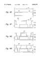
- WO 94/01885describes a PECVD process for depositing a multi-component dielectric layer wherein a silicon dioxide (SiO 2 ) liner layer 2 is first deposited on a patterned metal layer having metal lines 3 formed on a substrate 4.
- the liner layer 2is deposited by reaction of silane (SiH 4 ) and nitrous oxide (N 2 O).
- a self-planarizing low k dielectric layer 5is then deposited on the liner layer 2 by reaction of a silane compound and a peroxide compound.
- the liner layer 2is an oxidized silane film that has excellent barrier properties when deposited in a manner which provides a dielectric constant of about 4.5.
- the dielectric constant of the oxidized silane filmcan be decreased to about 4.1 by altering process conditions in a manner that decreases barrier properties of the film.
- WO 94/01885further describes an optional SiO 2 cap layer 6 that is deposited on the low k dielectric layer 5 by the reaction of silane and N 2 O.
- the cap layer 6is also an oxidized silane film that has excellent barrier properties when deposited in a manner which provides a dielectric constant of about 4.5.
- Both the liner layer 2 and the cap layer 6have a dielectric constant greater than 4.0 and the high dielectric constant layers substantially detract from the benefit of the low k dielectric layer.
- Silicon nitridehas been the etch stop material of choice for use with low k dielectric materials. However, the silicon nitride disposed between low k dielectric layers is within the fringing field between the interconnects. Silicon nitride has a relatively high dielectric constant (dielectric constant of about 7) compared to the surrounding dielectric, and it has been discovered that the silicon nitride may significantly increase the capacitive coupling between interconnect lines, even when an otherwise low k dielectric material is used as the primary insulator. This may lead to cross talk and/or resistance-capacitance (RC) delay which degrades the overall performance of the device.
- RCresistance-capacitance
- low k dielectric layerswhich have excellent barrier properties for use as liner or cap layers.
- low k dielectric layerswhich have sufficient oxide content for use as etch stop layers.
- the low k dielectric layerswould be compatible with existing low k dielectric materials and could be deposited in the same chambers as existing low k dielectric materials.
- the present inventionprovides a method and apparatus for deposition of a low dielectric constant layer which is produced by oxidation of an organo silane compound during plasma enhanced chemical vapor deposition.
- the oxidized organo silane layershave excellent barrier properties for use as a liner or cap layer adjacent other dielectric layers such as porous low k dielectric layers.
- the oxidized organo silane layershave can be used as an etch stop layer, as an adhesive layer between different layers, or as an intermetal dielectric layer.
- a preferred oxidized organ silane layeris produced by reaction of methyl silane, CH 3 SiH 3 , and nitrous oxide, N 2 O.
- a low k dielectric layeris deposited on a patterned metal layer by reaction of an organo silane compound and an oxidizing compound.
- a self-planarizing dielectric layeris then deposited in the same chamber by reaction of an organo-silane compound and a peroxide bonding compound.
- the self-planarizing dielectric layeris optionally capped in the same chamber by further reaction of the organo silane compound and the oxidizing compound.
- the liner and cap layersprovide strength to the self-planarizing dielectric layer during annealing of the self-planarizing dielectric layer. After annealing, the liner and cap layers serve as diffusion barriers which protect the self-planarizing dielectric layer.
- the present inventionfurther provides an etch stop material which provides a reliable dual damascene structure while minimizing the contribution of the etch stop layer to the capacitive coupling between interconnect lines.
- a low k dielectric filmsuch as an amorphous carbon ( ⁇ -C) or amorphous fluorinated carbon ( ⁇ -FC) film is used as the etch stop below an intermetal dielectric (IMD).
- IMDintermetal dielectric
- Other low k materialssuch as parylene, AF 4 , BCB, or PAE, or high k materials, such as oxynitride and silicon carbide, may also be used with the etch stop material.
- a preferred etch stop process sequencecomprises forming a dual damascene structure by depositing a first dielectric layer, such as parylene or a fluorinated silicate glass (FSG) layer, on a substrate, depositing the low k dielectric etch stop of the present invention on the first dielectric layer, patterning the etch stop to define the contacts/vias, depositing a second layer of a dielectric, patterning a resist layer on the second layer of dielectric to define one or more interconnects, and etching the interconnects and contacts/vias.
- the interconnectsare etched down to the etch stop, and then the etching continues past the patterned etch stop to define the contacts/vias.
- a barrier layeris preferably deposited conformably in the structure prior to filling the structure with copper to isolate the copper from other materials, such as silicon.
- the upper surfaceis then planarized using chemical mechanical polishing techniques.
- the inventionfurther provides an intermetal dielectric material comprising the low k dielectric film which is deposited on a conventional etch stop such as silicon oxide or silicon nitride.
- the low k dielectric filmcan also be deposited as a thin adhesive layer.
- FIGS. 1A-1Bare schematic diagrams of dielectric layers deposited on a substrate by the processes known in the art
- FIG. 2is a cross-sectional diagram of an exemplary CVD plasma reactor configured for use according to the present invention
- FIG. 3is a diagram of the system monitor of the CVD plasma reactor of FIG. 2;
- FIG. 4is a flowchart of a process control computer program product used in conjunction with the exemplary CVD plasma reactor of FIG. 2;
- FIG. 5is a flow chart illustrating steps undertaken in depositing liner and cap layers in a gap filling process according to one embodiment of the present invention
- FIGS. 6A-6Eis a schematic diagram of the layers deposited on a substrate by the process of FIG. 5;
- FIG. 7is a cross sectional view showing a dual damascene structure comprising the low k dielectric layers of the present invention.
- FIGS. 8A-8Hare cross sectional views showing one embodiment of a dual damascene deposition sequence of the present invention.
- FIG. 9is a cross sectional view showing an adhesive layer comprising the low k dielectric layers of the present invention between a premetal dielectric layer and an intermetal dielectric layer;
- FIGS. 10A-10Hare cross sectional views showing a dual damascene deposition sequence wherein the low k dielectric film of the present invention is used to adhere an intermetal dielectric film to a conventional etch stop.
- the present inventionprovides a method and apparatus for depositing a low dielectric constant layer which has excellent barrier properties and high oxide content.
- the low dielectric layeris an oxidized organo silane layer that can be used as a lining layer adjacent other dielectric materials, as an etch stop layer adjacent dielectric materials having lower oxide content, as an intermetal dielectric layer, and as an adhesion layer between different materials.
- the oxidized organo silane materialis deposited by oxidation of an organo silane compound which does not fully oxidize. Carbon, including some organo functional groups, which remains in the oxidized organo silane layer contribute to low dielectric constants and excellent barrier properties.
- the organo silane compoundsgenerally include the structure: ##STR1## wherein --C-- is included in an organo group and some C--Si bonds are not broken during oxidation.
- --C--is included in an alkyl, such as methyl or ethyl, or an aryl, such as phenyl.
- Suitable organo groupsalso can include alkenyl and cyclohexenyl groups and functional derivatives.
- the organo silane compoundsare oxidized during deposition by reaction with oxygen (O 2 ) or oxygen containing compounds such as nitrous oxide (N 2 O), preferably N 2 O, such that the carbon content of the deposited film is from 1 to 50% by atomic weight, preferably about 20%.
- the oxidized organo silane layerhas a dielectric constant of about 3.0 and has excellent barrier properties.
- the oxidized organo silane layersfurther have high oxide contents in comparison to conventional low k dielectric layers and good adhesion properties.
- the present inventionfurther provides a substrate processing system having a plasma reactor including a reaction zone, a substrate holder for positioning a substrate in the reaction zone, and a vacuum system.
- the processing systemfurther comprises a gas/liquid distribution system connecting the reaction zone of the vacuum chamber to supplies of an organo silane compound, an oxidizing gas, and an inert gas, and an RF generator coupled to the gas distribution system for generating a plasma in the reaction zone.
- the processing systemfurther comprises a controller comprising a computer for controlling the plasma reactor, the gas distribution system, and the RF generator, and a memory coupled to the controller, the memory comprising a computer usable medium comprising a computer readable program code for selecting the process steps of depositing a low dielectric constant film with a plasma of an organo silane compound and an oxidizing gas.
- the processing systemmay further comprise in one embodiment computer readable program code for selecting the process steps of depositing a liner of the oxidized organo silane compound, depositing a different dielectric layer, and optionally depositing a capping layer of the oxidized organo silane compound.
- FIG. 2is a vertical, cross-section view of a parallel plate chemical vapor deposition reactor 10 having a high vacuum region 15.
- Reactor 10contains a gas distribution manifold 11 for dispersing process gases through perforated holes in the manifold to a substrate or wafer (not shown) that rests on a substrate support plate or susceptor 12 which is raised or lowered by a lift motor 14.
- a liquid injection system(not shown), such as typically used for liquid injection of TEOS, may also be provided for injecting a liquid organo silane compound.
- the preferred methyl silanes and ethyl silanesare gases.
- the reactor 10includes heating of the process gases and substrate, such as by resistive heating coils (not shown) or external lamps (not shown).
- susceptor 12is mounted on a support stem 13 so that susceptor 12 (and the wafer supported on the upper surface of susceptor 12) can be controllably moved between a lower loading/off-loading position and an upper processing position which is closely adjacent to manifold 11.
- susceptor 12 and the waferWhen susceptor 12 and the wafer are in processing position 14, they are surrounded by a an insulator 17 and process gases exhaust into a manifold 24. During processing, gases inlet to manifold 11 are uniformly distributed radially across the surface of the wafer.
- a vacuum pump 32 having a throttle valvecontrols the exhaust rate of gases from the chamber.
- the process gases supply lines 18 for each of the process gasesinclude (i) safety shut-off valves (not shown) that can be used to automatically or manually shut off the flow of process gas into the chamber, and (ii) mass flow controllers (also not shown) that measure the flow of gas through the gas supply lines.
- safety shut-off valvesnot shown
- mass flow controllersalso not shown
- the deposition process performed in reactor 10can be either a thermal process or a plasma enhanced process.
- a controlled plasmais typically formed adjacent to the wafer by RF energy applied to distribution manifold 11 from RF power supply 25 (with susceptor 12 grounded).
- RF powercan be provided to the susceptor 12 or the RF power can be split between different components.
- RF power supply 25can supply either single or mixed frequency RF power to enhance the decomposition of reactive species introduced into the high vacuum region 15.
- a mixed frequency RF power supplytypically supplies power at a high RF frequency (RF1) of 13.56 MHZ and at a low RF frequency (RF2) of 360 KHz.
- any or all of the chamber lining, gas inlet manifold faceplate, support stem 13, and various other reactor hardwareis made out of material such as aluminum or anodized aluminum.
- An example of such a CVD reactoris described in U.S. Pat. No. 5,000,113, entitled “Thermal CVD/PECVD Reactor and Use for Thermal Chemical Vapor Deposition of Silicon Dioxide and In-situ Multi-step Planarized Process,” issued to Wang et al. And assigned to Applied Materials, Inc., the assignee of the present invention.
- the lift motor 14raises and lowers susceptor 12 between a processing position and a lower, wafer-loading position.
- the motor, the gas mixing system 19, and the RF power supply 25are controlled by a system controller 34 over control lines 36.
- the reactorincludes analog assemblies, such as mass flow controllers (MFCs) and RF generators, that are controlled by the system controller 34 which executes system control software stored in a memory 38, which in the preferred embodiment is a hard disk drive.
- MFCsmass flow controllers
- RF generatorsRF generators
- Motors and optical sensorsare used to move and determine the position of movable mechanical assemblies such as the throttle valve of the vacuum pump 32 and motor for positioning the susceptor 12.
- the system controller 34controls all of the activities of the CVD reactor and a preferred embodiment of the controller 34 includes a hard disk drive, a floppy disk drive, and a card rack.
- the card rackcontains a single board computer (SBC), analog and digital input/output boards, interface boards and stepper motor controller boards.
- SBCsingle board computer
- the system controllerconforms to the Versa Modular Europeans (VME) standard which defines board, card cage, and connector dimensions and types.
- VMEVersa Modular Europeans
- the VME standardalso defines the bus structure having a 16-bit data but and 24-bit address bus.
- the system controller 34operates under the control of a computer program stored on the hard disk drive 38.
- the computer programdictates the timing, mixture of gases, RF power levels, susceptor position, and other parameters of a particular process.
- the interface between a user and the system controlleris via a CRT monitor 40 and light pen 44 which are depicted in FIG. 3.
- a second monitor 42is used, the first monitor 40 being mounted in the clean room wall for the operators and the other monitor 42 behind the wall for the service technicians. Both monitors 40, 42 simultaneously display the same information but only one light pen 44 is enabled.
- the light pen 44detects light emitted by CRT display with a light sensor in the tip of the pen.
- the operatortouches a designated area of the display screen and pushes the button on the pen 44. The touched area changes its highlighted color, or a new menu or screen is displayed, confirming communication between the light pen and the display screen.
- the processcan be implemented using a computer program product 410 that runs on, for example, the system controller 34.
- the computer program codecan be written in any conventional computer readable programming language such as for example 68000 assembly language, C, C++, or Pascal. Suitable program code is entered into a single file, or multiple files, using a conventional text editor, and stored or embodied in a computer usable medium, such as a memory system of the computer. If the entered code text is in a high level language, the code is compiled, and the resultant compiler code is then linked with an object code of precompiled windows library routines. To execute the linked compiled object code, the system user invokes the object code, causing the computer system to load the code in memory, from which the CPU reads and executes the code to perform the tasks identified in the program
- FIG. 4shows an illustrative block diagram of the hierarchial control structure of the computer program 410.
- a userenters a process set number and process chamber number into a process selector subroutine 420 in response to menus or screens displayed on the CRT monitor 40 by using the light pen 44 interface.
- the process setsare predetermined sets of process parameters necessary to carry out specified processes, and are identified by predefined set numbers.
- the process selector subroutine 420the (i) selects a desired process chamber on a cluster tool such as an CenturaTM platform (available from Applied Materials, Inc.), and (ii) selects a desired set of process parameters needed to operate the process chamber for performing the desired process.
- the process parameters for performing a specific processrelate to process conditions such as, for example, process gas composition and flow rates, temperature, pressure, plasma conditions such as RF bias power levels and magnetic field power levels, cooling gas pressure, and chamber wall temperature and are provided to the user in the form of a recipe.
- process conditionssuch as, for example, process gas composition and flow rates, temperature, pressure, plasma conditions such as RF bias power levels and magnetic field power levels, cooling gas pressure, and chamber wall temperature and are provided to the user in the form of a recipe.
- the parameters specified by the recipeare entered utilizing the light pen/CRT monitor interface.
- the signals for monitoring the processare provided by the analog input and digital input boards of system controller and the signals for controlling the process are output on the analog output and digital output boards of the system controller 34.
- a process sequencer subroutine 430comprises program code for accepting the identified process chamber and set of process parameters from the process selector subroutine 420, and for controlling operation of the various process chambers. Multiple users can enter process set numbers and process chamber numbers, or a user can enter multiple process chamber numbers, so the sequencer subroutine 430 operates to schedule the selected processes in the desired sequence.
- the sequencer subroutine 430includes computer readable program code to perform the steps of (i) monitoring the operation of the process chambers to determine if the chambers are being used, (ii) determining what processes are being carried out in the chambers being used, and (iii) executing the desired process based on availability of a process chamber and type of process to be carried out.
- sequencer subroutine 430can be designed to take into consideration the present condition of the process chamber being used in comparison with the desired process conditions for a selected process, or the "age" of each particular user entered request, or any other relevant factor a system programmer desires to include for determining the scheduling priorities.
- the sequencer subroutine 430determines which process chamber and process set combination is going to be executed next, the sequencer subroutine 430 causes execution of the process set by passing the particular process set parameters to a chamber manager subroutine 440 which controls multiple processing tasks in a process chamber 10 according to the process set determined by the sequencer subroutine 430.
- the chamber manager subroutine 440comprises program code for controlling CVD process operations in the process chamber 10.
- the chamber manager subroutine 440also controls execution of various chamber component subroutines which control operation of the chamber component necessary to carry out the selected process set.
- chamber component subroutinesare susceptor control subroutine 450, process gas control subroutine 460, pressure control subroutine 470, heater control subroutine 480, and plasma control subroutine 490.
- process gas control subroutine 460processes gas control subroutine 460
- pressure control subroutine 470pressure control subroutine 470
- heater control subroutine 480heater control subroutine 480
- plasma control subroutine 490plasma control subroutine
- the chamber manager subroutine 440selectively schedules or calls the process component subroutines in accordance with the particular process set being executed.
- the chamber manager subroutine 440schedules the process component subroutines similarly to how the sequencer subroutine 430 schedules which process chamber 10 and process set is to be executed next.
- the chamber manager subroutine 440includes steps of monitoring the various chamber components, determining which components needs to be operated based on the process parameters for the process set to be executed, and causing execution of a chamber component subroutine responsive to the monitoring and determining steps.
- the susceptor control positioning subroutine 450comprises program code for controlling chamber components that are used to load the substrate onto the susceptor 12, and optionally to lift the substrate to a desired height in the reactor 10 to control the spacing between the substrate and the gas distribution manifold 11.
- the susceptor 12is lowered to receive the substrate, and thereafter, the susceptor 12 is raised to the desired height in the chamber, to maintain the substrate at a first distance or spacing from the gas distribution manifold 11 during the CVD process.
- the susceptor control subroutine 450controls movement of the susceptor 12 in response to process set parameters that are transferred from the chamber manager subroutine 440.
- the process gas control subroutine 460has program code for controlling process gas composition and flow rates.
- the process gas control subroutine 460controls the open/close position of the safety shut-off valves, and also ramps up/down the mass flow controllers to obtain the desired gas flow rate.
- the process gas control subroutine 460is invoked by the chamber manager subroutine 440, as are all chamber components subroutines, and receives from the chamber manager subroutine process parameters related to the desired gas flow rates.
- the process gas control subroutine 460operates by opening the gas supply lines, and repeatedly (i) reading the necessary mass flow controllers, (ii) comparing the readings to the desired flow rates received from the chamber manager subroutine 440, and (iii) adjusting the flow rates of the gas supply lines as necessary. Furthermore, the process gas control subroutine 460 includes steps for monitoring the gas flow rates for unsafe rates, and activating the safety shut-off valves when an unsafe condition is detected.
- an inert gassuch as helium or argon is flowed into the reactor 10 to stabilize the pressure in the chamber before reactive process gases are introduced into the chamber.
- the process gas control subroutine 460is programmed to include steps for flowing the inert gas into the chamber 10 for an amount of time necessary to stabilize the pressure in the chamber, and then the steps described above would be carried out. Additionally, when a process gas it to be vaporized from a liquid precursor, for example phenyl silane, the process gas control subroutine 460 would be written to include steps for bubbling a delivery gas such as helium through the liquid precursor in a bubbler assembly.
- the process gas control subroutine 460regulates the flow of the delivery gas, the pressure in the bubbler, and the bubbler temperature in order to obtain the desired process gas flow rates.
- the desired process gas flow ratesare transferred to the process gas control subroutine 460 as process parameters.
- the process gas control subroutine 460includes steps for obtaining the necessary delivery gas flow rate, bubbler pressure, and bubbler temperature for the desired process gas flow rate by accessing a stored table containing the necessary values for a given process gas flow rate. Once the necessary values are obtained, the delivery gas flow rate, bubbler pressure and bubbler temperature are monitored, compared to the necessary values and adjusted accordingly.
- the pressure control subroutine 470comprises program code for controlling the pressure in the reactor 10 by regulating the size of the opening of the throttle valve in the exhaust pump 32.
- the size of the opening of the throttle valveis set to control the chamber pressure to the desired level in relation to the total process gas flow, size of the process chamber, and pumping set point pressure for the exhaust pump 32.
- the pressure control subroutine 470is invoked, the desired, or target pressure level is received as a parameter from the chamber manager subroutine 440.
- the pressure control subroutine 470operates to measure the pressure in the reactor 10 by reading one or more conventional pressure manometers connected to the chamber, compare the measure value(s) to the target pressure, obtain PID (proportional, integral, and differential) values from a stored pressure table corresponding to the target pressure, and adjust the throttle valve according to the PID values obtained from the pressure table.
- the pressure control subroutine 470can be written to open or close the throttle valve to a particular opening size to regulate the reactor 10 to the desired pressure.
- the heater control subroutine 480comprises program code for controlling the temperature of the heat modules or radiated heat that is used to heat the susceptor 12.
- the heater control subroutine 480is also invoked by the chamber manager subroutine 440 and receives a target, or set point, temperature parameter.
- the heater control subroutine 480measures the temperature by measuring voltage output of a thermocouple located in a susceptor 12, compares the measured temperature to the set point temperature, and increases or decreases current applied to the heat module to obtain the set point temperature.
- the temperatureis obtained from the measured voltage by looking up the corresponding temperature in a stored conversion table, or by calculating the temperature using a fourth order polynomial.
- the heater control subroutine 480gradually controls a ramp up/down of current applied to the heat module. The gradual ramp up/down increases the life and reliability of the heat module. Additionally, a built-in-fail-safe mode can be included to detect process safety compliance, and can shut down operation of the heat module if the reactor 10 is not properly set
- the plasma control subroutine 490comprises program code for setting the RF bias voltage power level applied to the process electrodes in the reactor 10, and optionally, to set the level of the magnetic field generated in the reactor. Similar to the previously described chamber component subroutines, the plasma control subroutine 490 is invoked by the chamber manager subroutine 440.
- CVD system descriptionis mainly for illustrative purposes, and other plasma CVD equipment such as electrode cyclotron resonance (ECR) plasma CVD devices, induction-coupled RF high density plasma CVD devices, or the like may be employed. Additionally, variations of the above described system such as variations in susceptor design, heater design, location of RF power connections and others are possible. For example, the wafer could be supported and heated by a resistively heated susceptor.
- ECRelectrode cyclotron resonance
- the pretreatment and method for forming a pretreated layer of the present inventionis not limited to any specific apparatus or to any specific plasma excitation method.
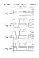
- the oxidized organo silane layer of the present inventioncan be used in a three-layer gap filling process as shown in FIG. 5 using the PECVD chamber of FIG. 2.
- a waferis positioned 200 in the reactor 10 and an oxidized organo silane layer having a low dielectric constant is deposited 205 by a PECVD process from a plasma comprising an organo silane compound, such as methyl silanes, ethyl silanes, or phenyl silanes, and an oxidizing gas.
- the deposition step 205can include a capacitively coupled plasma or both an inductively and a capacitively coupled plasma in the process chamber 15 according to methods known in the art.
- a gap fill layeris then deposited 210 on the liner layer by known methods.
- the gap fill layeris preferably self-planarizing, such as spin-on polymers or porous oxides deposited in liquid form by reaction of methyl silane and hydrogen peroxide.
- a cap layeris then deposited 215 on the gap fill layer, preferably using the same process for depositing the lining layer. The wafer is then removed 220 from the reactor 10.
- the three-layer gap filling processprovides a PECVD lining layer 300 of the oxidized organo silane polymer.
- the lining layer 300acts as an isolation layer between a subsequent PECVD gap fill layer 302 and the underlying substrate surface 304 and metal lines 306, 308, 310 formed on the substrate surface.
- the gap fill layer 302is capped by a PECVD capping layer 312 of the oxidized organo silane polymer. This process is implemented and controlled using a computer program stored in the memory 38 of a computer controller 34 for a CVD reactor 10.
- the PECVD lining layer 300is deposited in the reactor 10 by introducing an organo silane compound such as CH 3 SiH 3 , an oxidizing gas such as N 2 O, and a carrier gas such as helium.
- the substrateis maintained at a temperature of from about -10 to about 450° C., and preferably is maintained at a temperature of approximately 0° C. throughout the deposition of the PECVD lining layer.
- the PECVD lining layer 300is deposited with a process gas that includes a mixture of the organo silane compound at a flow rate of about 5 sccm to about 500 sccm and the oxidizing gas at a flow rate of about 5 sccm to about 2000 sccm.
- the process gasesare carried by an inert gas such He, Ar, Ne, or a relatively inert gas such as nitrogen, which are typically not incorporated into the film, at a flow rate of from about 0.2 to about 20 lpm.
- the process gasesreact at a pressure from about 0.2 to about 20 Torr to form a conformal polymer layer on the substrate surface 304 and metal lines 306, 308, 310, on the substrate surface.
- the reactionis plasma enhanced with a power density ranging from 0.05 W/cm 2 to 1000 W/cm 2 , preferably about 0.3 W/cm 2 .
- the high frequency RF source of approximately 13.56 MHzis preferably driven at about 30 to about 500 W and a low frequency RF source of about 350 KHz to MHz is preferably driven at about 0 to about 500 W.
- the high frequency RF sourceis driven at about 50-150 W, while the low frequency RF source is driven at about 0-100 W.
- the PECVD gap filling layer 302is deposited using similar reactor conditions as used for depositing the liner layer 300.
- the process gases for the gap filling layer 302are preferably SiH 4 , or CH 3 SiH 3 , and 50 wt% of hydrogen peroxide (H 2 O 2 ) which is vaporized and mixed with an inert carrier gas, such as helium.
- the gap filling layercan be any dielectric layer which has an acceptable dielectric constant.
- the process gas flowsrange from 0-2000 sccm for He, 10-200 sccm for CH 3 SiH 3 , and 0.1 to 3 g/min. for H 2 O 2 .
- the preferred gas flowsrange from 100-500 sccm for He, 20-100 sccm for CH 3 SiH 3 , and 0.1 to 1 g/min. for H 2 O 2 . These flow rates are given for a chamber having a volume of approximately 5.5 to 6.5 liters.
- reactor 10is maintained at a pressure of about 0.2 to about 5 torr during deposition of the PECVD gap filling layer 302.
- the gap filling layer 302may be partially cured as shown in FIG. 6C to remove solvents such as water prior to deposition of a cap layer 312 as shown in FIG. 6D. Curing is done in the reactor 10 by pumping under an inert gas atmosphere under 10 Torr.
- the reactor 10optionally resumes deposition of the oxidized organo silane layer of the present invention for deposition of a capping layer 312.
- the gap fill layer 302is preferably annealed in a furnace or another chamber at a temperature from about 100 to about 450 ° C. to drive off remaining solvent such as water.
- processing conditionswill vary according to the desired characteristics of the deposited films.
- a dual damascene structure which includes an oxidized organo silane layers as an etch stop or as an intermetal dielectric layeris shown in FIG. 7.
- a first dielectric layer 510is deposited on a substrate 512 and then the oxidized organo silane etch stop 514 is deposited on the first dielectric layer.
- the etch stopis then pattern etched to define the openings of the contacts/vias 516.
- a second dielectric layer 518is then deposited over the patterned etch stop and then pattern etched by conventional methods to define the interconnect lines 520.
- a single etch processis then performed to define the interconnects down to the etch stop and to etch the unprotected dielectric exposed by the patterned etch stop to define the contacts/vias.
- the damascene structurealternatively includes the oxidized organo silane as an intermetal dielectric.
- a first dielectric layer 510preferably consisting of the oxidized organo silane, is deposited on a substrate 512 and then a conventional silicon oxide or silicon nitride etch stop 514 is deposited on the first dielectric layer. The etch stop is then patterned to define the openings of the contacts/vias 516.
- a second dielectric layer 518, consisting of the oxidized organo silane,is then deposited over the patterned etch stop and then patterned to define the interconnect lines 520.
- a single etch processis then performed to define the interconnects down to the etch stop and to etch the unprotected dielectric exposed by the patterned etch stop to define the contacts/vias.
- a preferred dual damascene structure fabricated in accordance with the inventionincludes a lining layer as shown in FIG. 8H, and the method of making the structure is sequentially depicted schematically in FIGS. 8A-8H, which are cross sectional views of a substrate having the steps of the invention formed thereon.
- an initial first dielectric layer 510such as parylene, FSG, silicon oxide, or the like, is deposited on the substrate 512 to a thickness of about 5,000 to about 10,000 ⁇ , depending on the size of the structure to be fabricated.
- the low k etch stop 514which is the oxidized organo silane layer, is then deposited on the first dielectric layer to a thickness of about 200 to about 1000 ⁇ .
- Low k etch stop 514is then pattern etched to define the contact/via openings 516 and to expose first dielectric layer 510 in the areas where the contacts/vias are to be formed as shown in FIG. 8C.
- low k etch stop 514is pattern etched using conventional photolithography and etch processes using fluorine, carbon, and oxygen ions.
- a second dielectric layer 518is deposited over etch stop 514 to a thickness of about 5,000 to about 10,000 ⁇ as shown in FIG. 8D.
- a second dielectric layer 518is then patterned to define interconnect lines 520, preferably using conventional photolithography processes with a photo resist layer 522 as shown in FIG. 8E.
- interconnects and contacts/viasare then etched using reactive ion etching or other anisotropic etching techniques to define the metallization structure (i.e., the interconnect and contact/via) as shown in FIG. 8F.
- Any photo resist or other material used to pattern the etch stop 514 or the second dielectric layer 518is removed using an oxygen strip or other suitable process.
- the metallization structureis then formed with a conductive material such as aluminum, copper, tungsten or combinations thereof.
- a conductive materialsuch as aluminum, copper, tungsten or combinations thereof.
- the trendis to use copper to form the smaller features due to the low resistivity of copper (1.7 ⁇ -cm compared to 3.1 , ⁇ -cm for aluminum).
- a barrier layer 524 of the oxidized organo silane material, or other suitable barrieris first deposited conformally in the metallization pattern to prevent copper migration into the surrounding silicon and/or dielectric material.
- copper 526is deposited using either chemical vapor deposition, physical vapor deposition, electroplating, or combinations thereof to form the conductive structure.
- the surfaceis planarized using chemical mechanical polishing, as shown in FIG. 8H.
- a dual damascene structurewhich includes an oxidized organo silane layer as an adhesive layer between a premetal dielectric layer and an intermetal dielectric layer is shown in FIG. 9.
- the oxidized organo silane adhesive layer 612is deposited on a premetal dielectric layer 610 such as a conventional PSG or BPSG layer.
- An intermetal dielectric layer 614preferably a low k dielectric polymer layer, is then deposited over the adhesive layer 612.
- a conventional silicon oxide or silicon nitride etch stop 616is then patterned by conventional methods to define vias 620.
- a second intermetal dielectric layer 622preferably the low k dielectric polymer, is then deposited over the patterned etch stop and then patterned to define the interconnect lines.
- a single etch processis then performed to define the interconnects down to the etch stop and to etch the unprotected dielectric exposed by the patterned etch stop to define the contacts/vias prior to metallization.
- FIG. 10HA preferred dual damascene structure comprising an adhesive layer in accordance with the invention is shown in FIG. 10H, and the method of making the structure is sequentially depicted schematically in FIGS. 10A-10H, which are cross sectional views of a substrate having the steps of the invention formed thereon.
- an initial first intermetal dielectric layer 710such as parylene, FSG, silicon oxide, or the like, is deposited on a substrate 712 to a thickness of about 5,000 to about 10,000 ⁇ , depending on the size of the structure to be fabricated.
- a low k adhesive layer 714which is the oxidized organo silane layer, is then deposited on the first intermetal dielectric layer 710 to a thickness of about 50 to about 200 ⁇ .
- a conventional silicon oxide or silicon nitride etch stop 716is the deposited on the adhesive layer 714 to a thickness of about 50 to about 200 ⁇ .
- a second low k adhesive layer 718which is the oxidized organo silane layer, is then deposited on the etch stop 716 to a thickness of about 50 to about 200 ⁇ .
- the etch stop 716 and adhesive layers 714, 718are then pattern etched to define the contact/via openings 720 and to expose first intermetal dielectric layer 710 in the areas where the contacts/vias are to be formed as shown in FIG. 10C.
- the etch stop 716is pattern etched using conventional photolithography and etch processes using fluorine, carbon, and oxygen ions.
- a second intermetal dielectric layer 722is deposited over second adhesive layer 718 to a thickness of about 5,000 to about 10,000 ⁇ as shown in FIG. 10D.
- the second intermetal dielectric layer 722is then patterned to define interconnect lines 724, preferably using conventional photolithography processes with a photo resist layer 726 as shown in FIG. 10E.
- the interconnects and contacts/viasare then etched using reactive ion etching or other anisotropic etching techniques to define the metallization structure (i.e., the interconnect and contact/via) as shown in FIG. 10F.
- Any photo resist or other material used to pattern the etch stop 716 or the second intermetal dielectric layer 722is removed using an oxygen strip or other suitable process.
- the metallization structureis then formed with a conductive material such as aluminum, copper, tungsten or combinations thereof.
- a conductive materialsuch as aluminum, copper, tungsten or combinations thereof.
- the trendis to use copper to form the smaller features due to the low resistivity of copper (1.7 ⁇ -cm compared to 3.1 ⁇ -cm for aluminum).
- a barrier layer 728 of the oxidized organo silane material, or other suitable barrieris first deposited conformally in the metallization pattern to prevent copper migration into the surrounding silicon and/or dielectric material. Thereafter, copper is deposited using either chemical vapor deposition, physical vapor deposition, electroplating, or combinations thereof to form the conductive structure. Once the structure has been filled with copper or other metal, the surface is planarized using chemical mechanical polishing, as shown in FIG. 10H.
- the inventionis further described by the following example of a deposited methyl silane film.
- the following exampledemonstrates deposition of an oxidized organo silane film having excellent barrier and adhesion properties.
- This examplewas undertaken using a chemical vapor deposition chamber, and in particular, a "CENTURA DxZ" system which includes a solid-state RF matching unit with a two-piece quartz process kit, both fabricated and sold by Applied Materials, Inc., Santa Clara, Calif.
- the substratewas positioned 600 mil from the gas distribution showerhead and 80 W of high frequency power (13 MHz) was applied to the showerhead for plasma enhanced deposition of an oxidized methyl silane layer.
- the oxidized methyl silane materialwas deposited at a rate of 1800 ⁇ .
- the deposited filmhad a dielectric constant of 3.0 and a refractive index of 1.44.
- the filmhad a measured tensile stress of 0.8 ⁇ 10 9 dynes/cm 2 .
Landscapes
- Engineering & Computer Science (AREA)
- Physics & Mathematics (AREA)
- Condensed Matter Physics & Semiconductors (AREA)
- General Physics & Mathematics (AREA)
- Manufacturing & Machinery (AREA)
- Computer Hardware Design (AREA)
- Microelectronics & Electronic Packaging (AREA)
- Power Engineering (AREA)
- Chemical & Material Sciences (AREA)
- Inorganic Chemistry (AREA)
- General Chemical & Material Sciences (AREA)
- Chemical Kinetics & Catalysis (AREA)
- Materials Engineering (AREA)
- Mechanical Engineering (AREA)
- Metallurgy (AREA)
- Organic Chemistry (AREA)
- Internal Circuitry In Semiconductor Integrated Circuit Devices (AREA)
- Formation Of Insulating Films (AREA)
Abstract
Description
1.Field of the Invention
The present invention relates to the fabrication of integrated circuits. More particularly, the invention relates to a process and apparatus for depositing dielectric layers on a semiconductor substrate.
2. Background of the Invention
One of the primary steps in the fabrication of modem semiconductor devices is the formation of metal and dielectric films on a semiconductor substrate by chemical reaction of gases. Such deposition processes are referred to as chemical vapor deposition or CVD. Conventional thermal CVD processes supply reactive gases to the substrate surface where heat-induced chemical reactions take place to produce a desired film. The high temperatures at which some thermal CVD processes operate can damage device structures having layers previously formed thereon. A preferred method of depositing metal and dielectric films at relatively low temperatures is plasma-enhanced CVD (PECVD) techniques such as described in U.S. Pat. No. 5,362,526. Plasma-enhanced CVD techniques promote excitation and/or disassociation of the reactant gases by the application of radio frequency (RF) energy to a reaction zone near the substrate surface, thereby creating a plasma of highly reactive species. The high reactivity of the released species reduces the energy required for a chemical reaction to take place, and thus lowers the required temperature for such PECVD processes.
Semiconductor device geometries have dramatically decreased in size since such devices were first introduced several decades ago. Since then, integrated circuits have generally followed the two year/half-size rule (often called Moore's Law), which means that the number of devices that will fit on a chip doubles every two years. Today's wafer fabrication plants are routinely producing devices having 0.354μm and even 0.18μm feature sizes, and tomorrow's plants soon will be producing devices having even smaller geometries.
In order to further reduce the size of semiconductor devices on integrated circuits, it has become necessary to use conductive materials having low resistivity and insulators having low k (dielectric constant<4.0) to reduce the capacitive coupling between adjacent metal lines. For example, copper is now being considered as an interconnect material in place of aluminum because copper has a lower resistivity and higher current carrying capacity. However, these materials present new problems for integrated circuit manufacturing processes. For example, many low k dielectric materials are porous and are preferably protected by liner layers to prevent diffusion of metals. Conventional liner layers, such as SiN, have higher dielectric constants, and the combination of low k dielectric layers with high k dielectric liner layers may result in little or no improvement in the overall stack dielectric constant and capacitive coupling.
As shown in FIG. 1A, International Publication Number WO 94/01885 describes a PECVD process for depositing a multi-component dielectric layer wherein a silicon dioxide (SiO2)liner layer 2 is first deposited on a patterned metal layer havingmetal lines 3 formed on asubstrate 4. Theliner layer 2 is deposited by reaction of silane (SiH4) and nitrous oxide (N2 O). A self-planarizing low kdielectric layer 5 is then deposited on theliner layer 2 by reaction of a silane compound and a peroxide compound. Theliner layer 2 is an oxidized silane film that has excellent barrier properties when deposited in a manner which provides a dielectric constant of about 4.5. The dielectric constant of the oxidized silane film can be decreased to about 4.1 by altering process conditions in a manner that decreases barrier properties of the film.
As shown in FIG. 1B, WO 94/01885 further describes an optional SiO2 cap layer 6 that is deposited on the low kdielectric layer 5 by the reaction of silane and N2 O. Thecap layer 6 is also an oxidized silane film that has excellent barrier properties when deposited in a manner which provides a dielectric constant of about 4.5. Both theliner layer 2 and thecap layer 6 have a dielectric constant greater than 4.0 and the high dielectric constant layers substantially detract from the benefit of the low k dielectric layer.
The benefit of some low k dielectric materials is further compromised by low oxide content which makes the material inadequate as an etch stop layer. Silicon nitride has been the etch stop material of choice for use with low k dielectric materials. However, the silicon nitride disposed between low k dielectric layers is within the fringing field between the interconnects. Silicon nitride has a relatively high dielectric constant (dielectric constant of about 7) compared to the surrounding dielectric, and it has been discovered that the silicon nitride may significantly increase the capacitive coupling between interconnect lines, even when an otherwise low k dielectric material is used as the primary insulator. This may lead to cross talk and/or resistance-capacitance (RC) delay which degrades the overall performance of the device.
As devices get smaller, liner layers, cap layers, and etch stop layers contribute more to the overall dielectric constant of a multi-component dielectric layer. There remains a need for low k dielectric layers which have excellent barrier properties for use as liner or cap layers. There also remains a need for low k dielectric layers which have sufficient oxide content for use as etch stop layers. Ideally, the low k dielectric layers would be compatible with existing low k dielectric materials and could be deposited in the same chambers as existing low k dielectric materials.
The present invention provides a method and apparatus for deposition of a low dielectric constant layer which is produced by oxidation of an organo silane compound during plasma enhanced chemical vapor deposition. The oxidized organo silane layers have excellent barrier properties for use as a liner or cap layer adjacent other dielectric layers such as porous low k dielectric layers. In addition, the oxidized organo silane layers have can be used as an etch stop layer, as an adhesive layer between different layers, or as an intermetal dielectric layer. A preferred oxidized organ silane layer is produced by reaction of methyl silane, CH3 SiH3, and nitrous oxide, N2 O.
In a preferred embodiment, a low k dielectric layer is deposited on a patterned metal layer by reaction of an organo silane compound and an oxidizing compound. A self-planarizing dielectric layer is then deposited in the same chamber by reaction of an organo-silane compound and a peroxide bonding compound. The self-planarizing dielectric layer is optionally capped in the same chamber by further reaction of the organo silane compound and the oxidizing compound. The liner and cap layers provide strength to the self-planarizing dielectric layer during annealing of the self-planarizing dielectric layer. After annealing, the liner and cap layers serve as diffusion barriers which protect the self-planarizing dielectric layer.
The present invention further provides an etch stop material which provides a reliable dual damascene structure while minimizing the contribution of the etch stop layer to the capacitive coupling between interconnect lines. In a preferred embodiment, a low k dielectric film, such as an amorphous carbon (∝-C) or amorphous fluorinated carbon (∝-FC) film is used as the etch stop below an intermetal dielectric (IMD). Other low k materials, such as parylene, AF4, BCB, or PAE, or high k materials, such as oxynitride and silicon carbide, may also be used with the etch stop material.
A preferred etch stop process sequence comprises forming a dual damascene structure by depositing a first dielectric layer, such as parylene or a fluorinated silicate glass (FSG) layer, on a substrate, depositing the low k dielectric etch stop of the present invention on the first dielectric layer, patterning the etch stop to define the contacts/vias, depositing a second layer of a dielectric, patterning a resist layer on the second layer of dielectric to define one or more interconnects, and etching the interconnects and contacts/vias. The interconnects are etched down to the etch stop, and then the etching continues past the patterned etch stop to define the contacts/vias. Once the dual damascene structure has been formed, a barrier layer is preferably deposited conformably in the structure prior to filling the structure with copper to isolate the copper from other materials, such as silicon. The upper surface is then planarized using chemical mechanical polishing techniques.
The invention further provides an intermetal dielectric material comprising the low k dielectric film which is deposited on a conventional etch stop such as silicon oxide or silicon nitride. The low k dielectric film can also be deposited as a thin adhesive layer.
So that the manner in which the above recited features, advantages and objects of the present invention are attained and can be understood in detail, a more particular description of the invention, briefly summarized above, may be had by reference to the embodiments thereof which are illustrated in the appended drawings.
It is to be noted, however, that the appended drawings illustrate only typical embodiments of this invention and are therefore not to be considered limiting of its scope, for the invention may admit to other equally effective embodiments.
FIGS. 1A-1B (Prior Art) are schematic diagrams of dielectric layers deposited on a substrate by the processes known in the art;
FIG. 2 is a cross-sectional diagram of an exemplary CVD plasma reactor configured for use according to the present invention;
FIG. 3 is a diagram of the system monitor of the CVD plasma reactor of FIG. 2;
FIG. 4 is a flowchart of a process control computer program product used in conjunction with the exemplary CVD plasma reactor of FIG. 2;
FIG. 5 is a flow chart illustrating steps undertaken in depositing liner and cap layers in a gap filling process according to one embodiment of the present invention;
FIGS. 6A-6E is a schematic diagram of the layers deposited on a substrate by the process of FIG. 5;
FIG. 7 is a cross sectional view showing a dual damascene structure comprising the low k dielectric layers of the present invention;
FIGS. 8A-8H are cross sectional views showing one embodiment of a dual damascene deposition sequence of the present invention;
FIG. 9 is a cross sectional view showing an adhesive layer comprising the low k dielectric layers of the present invention between a premetal dielectric layer and an intermetal dielectric layer; and
FIGS. 10A-10H are cross sectional views showing a dual damascene deposition sequence wherein the low k dielectric film of the present invention is used to adhere an intermetal dielectric film to a conventional etch stop.
For a further understanding of the present invention, reference should be made to the ensuing detailed description.
The present invention provides a method and apparatus for depositing a low dielectric constant layer which has excellent barrier properties and high oxide content. The low dielectric layer is an oxidized organo silane layer that can be used as a lining layer adjacent other dielectric materials, as an etch stop layer adjacent dielectric materials having lower oxide content, as an intermetal dielectric layer, and as an adhesion layer between different materials. The oxidized organo silane material is deposited by oxidation of an organo silane compound which does not fully oxidize. Carbon, including some organo functional groups, which remains in the oxidized organo silane layer contribute to low dielectric constants and excellent barrier properties.
The organo silane compounds generally include the structure: ##STR1## wherein --C-- is included in an organo group and some C--Si bonds are not broken during oxidation. Preferably --C-- is included in an alkyl, such as methyl or ethyl, or an aryl, such as phenyl. Suitable organo groups also can include alkenyl and cyclohexenyl groups and functional derivatives. The preferred organo silane compounds have the structure SiHa (CH3)b (C2 H5)c (C6 H5)d, where a=1 to 3, b=0 to 3, c=0 to 3, d=0 to 3, and a+b+c+d=4 or the structure Si2 He (CH3)f (C2 H5)g (C6 H5)h, where e=1 to 5, f=0 to 5, g=0 to 5, h=0 to 5, and e+f+g+h=6. Preferred organo silane compounds include methyl silane compounds having the structure SiHn (CH3)4-n, where n=1 to 3, i.e. methyl silane, dimethyl silane, or trimethyl silane or the structure Si2 Hm (CH3)6-m, where m=1 to 5. The most preferred organo silane compound is methyl silane, CH3 SiH3. The organo silane compounds are oxidized during deposition by reaction with oxygen (O2) or oxygen containing compounds such as nitrous oxide (N2 O), preferably N2 O, such that the carbon content of the deposited film is from 1 to 50% by atomic weight, preferably about 20%. The oxidized organo silane layer has a dielectric constant of about 3.0 and has excellent barrier properties. The oxidized organo silane layers further have high oxide contents in comparison to conventional low k dielectric layers and good adhesion properties.
The present invention further provides a substrate processing system having a plasma reactor including a reaction zone, a substrate holder for positioning a substrate in the reaction zone, and a vacuum system. The processing system further comprises a gas/liquid distribution system connecting the reaction zone of the vacuum chamber to supplies of an organo silane compound, an oxidizing gas, and an inert gas, and an RF generator coupled to the gas distribution system for generating a plasma in the reaction zone. The processing system further comprises a controller comprising a computer for controlling the plasma reactor, the gas distribution system, and the RF generator, and a memory coupled to the controller, the memory comprising a computer usable medium comprising a computer readable program code for selecting the process steps of depositing a low dielectric constant film with a plasma of an organo silane compound and an oxidizing gas.
The processing system may further comprise in one embodiment computer readable program code for selecting the process steps of depositing a liner of the oxidized organo silane compound, depositing a different dielectric layer, and optionally depositing a capping layer of the oxidized organo silane compound.
Further description of the invention will be directed toward specific embodiments.
Exemplary CVD Plasma Reactor
One suitable CVD plasma reactor in which a method of the present invention can be carried out is shown in FIG. 2, which is a vertical, cross-section view of a parallel plate chemicalvapor deposition reactor 10 having ahigh vacuum region 15.Reactor 10 contains agas distribution manifold 11 for dispersing process gases through perforated holes in the manifold to a substrate or wafer (not shown) that rests on a substrate support plate orsusceptor 12 which is raised or lowered by alift motor 14. A liquid injection system (not shown), such as typically used for liquid injection of TEOS, may also be provided for injecting a liquid organo silane compound. The preferred methyl silanes and ethyl silanes are gases.
Thereactor 10 includes heating of the process gases and substrate, such as by resistive heating coils (not shown) or external lamps (not shown). Referring to FIG. 2,susceptor 12 is mounted on asupport stem 13 so that susceptor 12 (and the wafer supported on the upper surface of susceptor 12) can be controllably moved between a lower loading/off-loading position and an upper processing position which is closely adjacent tomanifold 11.
When susceptor 12 and the wafer are in processingposition 14, they are surrounded by a an insulator 17 and process gases exhaust into amanifold 24. During processing, gases inlet tomanifold 11 are uniformly distributed radially across the surface of the wafer. Avacuum pump 32 having a throttle valve controls the exhaust rate of gases from the chamber.
Before reachingmanifold 11, deposition and carrier gases are input throughgas lines 18 into amixing system 19 where they are combined and then sent tomanifold 11. Generally, the process gases supplylines 18 for each of the process gases include (i) safety shut-off valves (not shown) that can be used to automatically or manually shut off the flow of process gas into the chamber, and (ii) mass flow controllers (also not shown) that measure the flow of gas through the gas supply lines. When toxic gases are used in the process, several safety shut-off valves are positioned on each gas supply line in conventional configurations.
The deposition process performed inreactor 10 can be either a thermal process or a plasma enhanced process. In a plasma process, a controlled plasma is typically formed adjacent to the wafer by RF energy applied todistribution manifold 11 from RF power supply 25 (withsusceptor 12 grounded). Alternatively, RF power can be provided to thesusceptor 12 or the RF power can be split between different components.RF power supply 25 can supply either single or mixed frequency RF power to enhance the decomposition of reactive species introduced into thehigh vacuum region 15. A mixed frequency RF power supply typically supplies power at a high RF frequency (RF1) of 13.56 MHZ and at a low RF frequency (RF2) of 360 KHz.
Typically, any or all of the chamber lining, gas inlet manifold faceplate,support stem 13, and various other reactor hardware is made out of material such as aluminum or anodized aluminum. An example of such a CVD reactor is described in U.S. Pat. No. 5,000,113, entitled "Thermal CVD/PECVD Reactor and Use for Thermal Chemical Vapor Deposition of Silicon Dioxide and In-situ Multi-step Planarized Process," issued to Wang et al. And assigned to Applied Materials, Inc., the assignee of the present invention.
Thelift motor 14 raises and lowerssusceptor 12 between a processing position and a lower, wafer-loading position. The motor, thegas mixing system 19, and theRF power supply 25 are controlled by asystem controller 34 over control lines 36. The reactor includes analog assemblies, such as mass flow controllers (MFCs) and RF generators, that are controlled by thesystem controller 34 which executes system control software stored in amemory 38, which in the preferred embodiment is a hard disk drive. Motors and optical sensors are used to move and determine the position of movable mechanical assemblies such as the throttle valve of thevacuum pump 32 and motor for positioning thesusceptor 12.
Thesystem controller 34 controls all of the activities of the CVD reactor and a preferred embodiment of thecontroller 34 includes a hard disk drive, a floppy disk drive, and a card rack. The card rack contains a single board computer (SBC), analog and digital input/output boards, interface boards and stepper motor controller boards. The system controller conforms to the Versa Modular Europeans (VME) standard which defines board, card cage, and connector dimensions and types. The VME standard also defines the bus structure having a 16-bit data but and 24-bit address bus.
Thesystem controller 34 operates under the control of a computer program stored on thehard disk drive 38. The computer program dictates the timing, mixture of gases, RF power levels, susceptor position, and other parameters of a particular process. The interface between a user and the system controller is via aCRT monitor 40 andlight pen 44 which are depicted in FIG. 3. In the preferred embodiment asecond monitor 42 is used, thefirst monitor 40 being mounted in the clean room wall for the operators and theother monitor 42 behind the wall for the service technicians. Both monitors 40, 42 simultaneously display the same information but only onelight pen 44 is enabled. Thelight pen 44 detects light emitted by CRT display with a light sensor in the tip of the pen. To select a particular screen or function, the operator touches a designated area of the display screen and pushes the button on thepen 44. The touched area changes its highlighted color, or a new menu or screen is displayed, confirming communication between the light pen and the display screen.
Referring to FIG. 4, the process can be implemented using acomputer program product 410 that runs on, for example, thesystem controller 34. The computer program code can be written in any conventional computer readable programming language such as for example 68000 assembly language, C, C++, or Pascal. Suitable program code is entered into a single file, or multiple files, using a conventional text editor, and stored or embodied in a computer usable medium, such as a memory system of the computer. If the entered code text is in a high level language, the code is compiled, and the resultant compiler code is then linked with an object code of precompiled windows library routines. To execute the linked compiled object code, the system user invokes the object code, causing the computer system to load the code in memory, from which the CPU reads and executes the code to perform the tasks identified in the program
FIG. 4 shows an illustrative block diagram of the hierarchial control structure of thecomputer program 410. A user enters a process set number and process chamber number into aprocess selector subroutine 420 in response to menus or screens displayed on the CRT monitor 40 by using thelight pen 44 interface. The process sets are predetermined sets of process parameters necessary to carry out specified processes, and are identified by predefined set numbers. Theprocess selector subroutine 420 the (i) selects a desired process chamber on a cluster tool such as an Centura™ platform (available from Applied Materials, Inc.), and (ii) selects a desired set of process parameters needed to operate the process chamber for performing the desired process. The process parameters for performing a specific process relate to process conditions such as, for example, process gas composition and flow rates, temperature, pressure, plasma conditions such as RF bias power levels and magnetic field power levels, cooling gas pressure, and chamber wall temperature and are provided to the user in the form of a recipe. The parameters specified by the recipe are entered utilizing the light pen/CRT monitor interface.
The signals for monitoring the process are provided by the analog input and digital input boards of system controller and the signals for controlling the process are output on the analog output and digital output boards of thesystem controller 34.
Aprocess sequencer subroutine 430 comprises program code for accepting the identified process chamber and set of process parameters from theprocess selector subroutine 420, and for controlling operation of the various process chambers. Multiple users can enter process set numbers and process chamber numbers, or a user can enter multiple process chamber numbers, so thesequencer subroutine 430 operates to schedule the selected processes in the desired sequence. Preferably thesequencer subroutine 430 includes computer readable program code to perform the steps of (i) monitoring the operation of the process chambers to determine if the chambers are being used, (ii) determining what processes are being carried out in the chambers being used, and (iii) executing the desired process based on availability of a process chamber and type of process to be carried out. Conventional methods of monitoring the process chambers can be used, such as polling. When scheduling which process is to be executed, thesequencer subroutine 430 can be designed to take into consideration the present condition of the process chamber being used in comparison with the desired process conditions for a selected process, or the "age" of each particular user entered request, or any other relevant factor a system programmer desires to include for determining the scheduling priorities.
Once thesequencer subroutine 430 determines which process chamber and process set combination is going to be executed next, thesequencer subroutine 430 causes execution of the process set by passing the particular process set parameters to achamber manager subroutine 440 which controls multiple processing tasks in aprocess chamber 10 according to the process set determined by thesequencer subroutine 430. For example, thechamber manager subroutine 440 comprises program code for controlling CVD process operations in theprocess chamber 10. Thechamber manager subroutine 440 also controls execution of various chamber component subroutines which control operation of the chamber component necessary to carry out the selected process set. Examples of chamber component subroutines aresusceptor control subroutine 450, processgas control subroutine 460,pressure control subroutine 470,heater control subroutine 480, andplasma control subroutine 490. Those having ordinary skill in the art would readily recognize that other chamber control subroutines can be included depending on what processes are desired to be performed in thereactor 10.
In operation, thechamber manager subroutine 440 selectively schedules or calls the process component subroutines in accordance with the particular process set being executed. Thechamber manager subroutine 440 schedules the process component subroutines similarly to how thesequencer subroutine 430 schedules whichprocess chamber 10 and process set is to be executed next. Typically, thechamber manager subroutine 440 includes steps of monitoring the various chamber components, determining which components needs to be operated based on the process parameters for the process set to be executed, and causing execution of a chamber component subroutine responsive to the monitoring and determining steps.
Operation of particular chamber components subroutines will now be described with reference to FIG. 4. The susceptorcontrol positioning subroutine 450 comprises program code for controlling chamber components that are used to load the substrate onto thesusceptor 12, and optionally to lift the substrate to a desired height in thereactor 10 to control the spacing between the substrate and thegas distribution manifold 11. When a substrate is loaded into thereactor 10, thesusceptor 12 is lowered to receive the substrate, and thereafter, thesusceptor 12 is raised to the desired height in the chamber, to maintain the substrate at a first distance or spacing from thegas distribution manifold 11 during the CVD process. In operation, thesusceptor control subroutine 450 controls movement of thesusceptor 12 in response to process set parameters that are transferred from thechamber manager subroutine 440.
The processgas control subroutine 460 has program code for controlling process gas composition and flow rates. The processgas control subroutine 460 controls the open/close position of the safety shut-off valves, and also ramps up/down the mass flow controllers to obtain the desired gas flow rate. The processgas control subroutine 460 is invoked by thechamber manager subroutine 440, as are all chamber components subroutines, and receives from the chamber manager subroutine process parameters related to the desired gas flow rates. Typically, the processgas control subroutine 460 operates by opening the gas supply lines, and repeatedly (i) reading the necessary mass flow controllers, (ii) comparing the readings to the desired flow rates received from thechamber manager subroutine 440, and (iii) adjusting the flow rates of the gas supply lines as necessary. Furthermore, the processgas control subroutine 460 includes steps for monitoring the gas flow rates for unsafe rates, and activating the safety shut-off valves when an unsafe condition is detected.
In some processes, an inert gas such as helium or argon is flowed into thereactor 10 to stabilize the pressure in the chamber before reactive process gases are introduced into the chamber. For these processes, the processgas control subroutine 460 is programmed to include steps for flowing the inert gas into thechamber 10 for an amount of time necessary to stabilize the pressure in the chamber, and then the steps described above would be carried out. Additionally, when a process gas it to be vaporized from a liquid precursor, for example phenyl silane, the processgas control subroutine 460 would be written to include steps for bubbling a delivery gas such as helium through the liquid precursor in a bubbler assembly. For this type of process, the processgas control subroutine 460 regulates the flow of the delivery gas, the pressure in the bubbler, and the bubbler temperature in order to obtain the desired process gas flow rates. As discussed above, the desired process gas flow rates are transferred to the processgas control subroutine 460 as process parameters. Furthermore, the processgas control subroutine 460 includes steps for obtaining the necessary delivery gas flow rate, bubbler pressure, and bubbler temperature for the desired process gas flow rate by accessing a stored table containing the necessary values for a given process gas flow rate. Once the necessary values are obtained, the delivery gas flow rate, bubbler pressure and bubbler temperature are monitored, compared to the necessary values and adjusted accordingly.
Thepressure control subroutine 470 comprises program code for controlling the pressure in thereactor 10 by regulating the size of the opening of the throttle valve in theexhaust pump 32. The size of the opening of the throttle valve is set to control the chamber pressure to the desired level in relation to the total process gas flow, size of the process chamber, and pumping set point pressure for theexhaust pump 32. When thepressure control subroutine 470 is invoked, the desired, or target pressure level is received as a parameter from thechamber manager subroutine 440. Thepressure control subroutine 470 operates to measure the pressure in thereactor 10 by reading one or more conventional pressure manometers connected to the chamber, compare the measure value(s) to the target pressure, obtain PID (proportional, integral, and differential) values from a stored pressure table corresponding to the target pressure, and adjust the throttle valve according to the PID values obtained from the pressure table. Alternatively, thepressure control subroutine 470 can be written to open or close the throttle valve to a particular opening size to regulate thereactor 10 to the desired pressure.
Theheater control subroutine 480 comprises program code for controlling the temperature of the heat modules or radiated heat that is used to heat thesusceptor 12. Theheater control subroutine 480 is also invoked by thechamber manager subroutine 440 and receives a target, or set point, temperature parameter. Theheater control subroutine 480 measures the temperature by measuring voltage output of a thermocouple located in asusceptor 12, compares the measured temperature to the set point temperature, and increases or decreases current applied to the heat module to obtain the set point temperature. The temperature is obtained from the measured voltage by looking up the corresponding temperature in a stored conversion table, or by calculating the temperature using a fourth order polynomial. Theheater control subroutine 480 gradually controls a ramp up/down of current applied to the heat module. The gradual ramp up/down increases the life and reliability of the heat module. Additionally, a built-in-fail-safe mode can be included to detect process safety compliance, and can shut down operation of the heat module if thereactor 10 is not properly set up.
Theplasma control subroutine 490 comprises program code for setting the RF bias voltage power level applied to the process electrodes in thereactor 10, and optionally, to set the level of the magnetic field generated in the reactor. Similar to the previously described chamber component subroutines, theplasma control subroutine 490 is invoked by thechamber manager subroutine 440.
The above CVD system description is mainly for illustrative purposes, and other plasma CVD equipment such as electrode cyclotron resonance (ECR) plasma CVD devices, induction-coupled RF high density plasma CVD devices, or the like may be employed. Additionally, variations of the above described system such as variations in susceptor design, heater design, location of RF power connections and others are possible. For example, the wafer could be supported and heated by a resistively heated susceptor. The pretreatment and method for forming a pretreated layer of the present invention is not limited to any specific apparatus or to any specific plasma excitation method.
Deposition of the Oxidized Organo Silane Dielectric in a Three-Layer Gap Filling Process
The oxidized organo silane layer of the present invention can be used in a three-layer gap filling process as shown in FIG. 5 using the PECVD chamber of FIG. 2. Referring to FIG. 5, a wafer is positioned 200 in thereactor 10 and an oxidized organo silane layer having a low dielectric constant is deposited 205 by a PECVD process from a plasma comprising an organo silane compound, such as methyl silanes, ethyl silanes, or phenyl silanes, and an oxidizing gas. Thedeposition step 205 can include a capacitively coupled plasma or both an inductively and a capacitively coupled plasma in theprocess chamber 15 according to methods known in the art. An inert gas such as helium is commonly used in the PECVD deposition to assist in plasma generation. A gap fill layer is then deposited 210 on the liner layer by known methods. The gap fill layer is preferably self-planarizing, such as spin-on polymers or porous oxides deposited in liquid form by reaction of methyl silane and hydrogen peroxide. A cap layer is then deposited 215 on the gap fill layer, preferably using the same process for depositing the lining layer. The wafer is then removed 220 from thereactor 10.
Referring to FIGS. 6A-6E, the three-layer gap filling process provides aPECVD lining layer 300 of the oxidized organo silane polymer. Thelining layer 300 acts as an isolation layer between a subsequent PECVDgap fill layer 302 and theunderlying substrate surface 304 andmetal lines gap fill layer 302 is capped by aPECVD capping layer 312 of the oxidized organo silane polymer. This process is implemented and controlled using a computer program stored in thememory 38 of acomputer controller 34 for aCVD reactor 10.
Referring to FIG. 6A, thePECVD lining layer 300 is deposited in thereactor 10 by introducing an organo silane compound such as CH3 SiH3, an oxidizing gas such as N2 O, and a carrier gas such as helium. The substrate is maintained at a temperature of from about -10 to about 450° C., and preferably is maintained at a temperature of approximately 0° C. throughout the deposition of the PECVD lining layer. ThePECVD lining layer 300 is deposited with a process gas that includes a mixture of the organo silane compound at a flow rate of about 5 sccm to about 500 sccm and the oxidizing gas at a flow rate of about 5 sccm to about 2000 sccm. The process gases are carried by an inert gas such He, Ar, Ne, or a relatively inert gas such as nitrogen, which are typically not incorporated into the film, at a flow rate of from about 0.2 to about 20 lpm. The process gases react at a pressure from about 0.2 to about 20 Torr to form a conformal polymer layer on thesubstrate surface 304 andmetal lines
For an 8" single wafer chamber, the high frequency RF source of approximately 13.56 MHz is preferably driven at about 30 to about 500 W and a low frequency RF source of about 350 KHz to MHz is preferably driven at about 0 to about 500 W. In a currently preferred embodiment, the high frequency RF source is driven at about 50-150 W, while the low frequency RF source is driven at about 0-100 W.
The above process conditions result in the deposition of a PECVD lining layer 300 (at about 2000 Å per minute) with improved barrier characteristics for the subsequent deposition of the PECVDgap filling layer 302.
Referring to FIG. 6B, the PECVDgap filling layer 302 is deposited using similar reactor conditions as used for depositing theliner layer 300. The process gases for thegap filling layer 302 are preferably SiH4, or CH3 SiH3, and 50 wt% of hydrogen peroxide (H2 O2) which is vaporized and mixed with an inert carrier gas, such as helium. However, the gap filling layer can be any dielectric layer which has an acceptable dielectric constant. The process gas flows range from 0-2000 sccm for He, 10-200 sccm for CH3 SiH3, and 0.1 to 3 g/min. for H2 O2. The preferred gas flows range from 100-500 sccm for He, 20-100 sccm for CH3 SiH3, and 0.1 to 1 g/min. for H2 O2. These flow rates are given for a chamber having a volume of approximately 5.5 to 6.5 liters. Preferably,reactor 10 is maintained at a pressure of about 0.2 to about 5 torr during deposition of the PECVDgap filling layer 302. Thegap filling layer 302 may be partially cured as shown in FIG. 6C to remove solvents such as water prior to deposition of acap layer 312 as shown in FIG. 6D. Curing is done in thereactor 10 by pumping under an inert gas atmosphere under 10 Torr.
Referring to FIG. 6D, after deposition of the PECVDgap filling layer 302, thereactor 10 optionally resumes deposition of the oxidized organo silane layer of the present invention for deposition of acapping layer 312. Referring to FIG. 6E, after deposition of the capping layer, if any, thegap fill layer 302 is preferably annealed in a furnace or another chamber at a temperature from about 100 to about 450 ° C. to drive off remaining solvent such as water. Of course, processing conditions will vary according to the desired characteristics of the deposited films.
Deposition of a Dual Damascene Structure
A dual damascene structure which includes an oxidized organo silane layers as an etch stop or as an intermetal dielectric layer is shown in FIG. 7. When the oxidized organo silane is used as an etch stop, a firstdielectric layer 510 is deposited on asubstrate 512 and then the oxidized organosilane etch stop 514 is deposited on the first dielectric layer. The etch stop is then pattern etched to define the openings of the contacts/vias 516. Asecond dielectric layer 518 is then deposited over the patterned etch stop and then pattern etched by conventional methods to define the interconnect lines 520. A single etch process is then performed to define the interconnects down to the etch stop and to etch the unprotected dielectric exposed by the patterned etch stop to define the contacts/vias.
Referring again to FIG. 7, the damascene structure alternatively includes the oxidized organo silane as an intermetal dielectric. Afirst dielectric layer 510, preferably consisting of the oxidized organo silane, is deposited on asubstrate 512 and then a conventional silicon oxide or siliconnitride etch stop 514 is deposited on the first dielectric layer. The etch stop is then patterned to define the openings of the contacts/vias 516. Asecond dielectric layer 518, consisting of the oxidized organo silane, is then deposited over the patterned etch stop and then patterned to define the interconnect lines 520. A single etch process is then performed to define the interconnects down to the etch stop and to etch the unprotected dielectric exposed by the patterned etch stop to define the contacts/vias.
A preferred dual damascene structure fabricated in accordance with the invention includes a lining layer as shown in FIG. 8H, and the method of making the structure is sequentially depicted schematically in FIGS. 8A-8H, which are cross sectional views of a substrate having the steps of the invention formed thereon.
As shown in FIG. 8A, an initial firstdielectric layer 510, such as parylene, FSG, silicon oxide, or the like, is deposited on thesubstrate 512 to a thickness of about 5,000 to about 10,000 Å, depending on the size of the structure to be fabricated. As shown in FIG. 8B, the lowk etch stop 514, which is the oxidized organo silane layer, is then deposited on the first dielectric layer to a thickness of about 200 to about 1000 Å. Lowk etch stop 514 is then pattern etched to define the contact/viaopenings 516 and to expose firstdielectric layer 510 in the areas where the contacts/vias are to be formed as shown in FIG. 8C. Preferably, lowk etch stop 514 is pattern etched using conventional photolithography and etch processes using fluorine, carbon, and oxygen ions. After lowk etch stop 514 has been etched to pattern the contacts/vias and the photo resist has been removed, asecond dielectric layer 518 is deposited over etch stop 514 to a thickness of about 5,000 to about 10,000 Å as shown in FIG. 8D. Asecond dielectric layer 518 is then patterned to defineinterconnect lines 520, preferably using conventional photolithography processes with a photo resistlayer 522 as shown in FIG. 8E. The interconnects and contacts/vias are then etched using reactive ion etching or other anisotropic etching techniques to define the metallization structure (i.e., the interconnect and contact/via) as shown in FIG. 8F. Any photo resist or other material used to pattern the etch stop 514 or thesecond dielectric layer 518 is removed using an oxygen strip or other suitable process.
The metallization structure is then formed with a conductive material such as aluminum, copper, tungsten or combinations thereof. Presently, the trend is to use copper to form the smaller features due to the low resistivity of copper (1.7 μΩ-cm compared to 3.1 ,μΩ-cm for aluminum). Preferably, as shown in FIG. 8G, abarrier layer 524 of the oxidized organo silane material, or other suitable barrier is first deposited conformally in the metallization pattern to prevent copper migration into the surrounding silicon and/or dielectric material. Thereafter, as shown in FIG. 8H,copper 526 is deposited using either chemical vapor deposition, physical vapor deposition, electroplating, or combinations thereof to form the conductive structure. Once the structure has been filled with copper or other metal, the surface is planarized using chemical mechanical polishing, as shown in FIG. 8H.
Deposition of Adhesive Layers
A dual damascene structure which includes an oxidized organo silane layer as an adhesive layer between a premetal dielectric layer and an intermetal dielectric layer is shown in FIG. 9. The oxidized organosilane adhesive layer 612 is deposited on apremetal dielectric layer 610 such as a conventional PSG or BPSG layer. An intermetaldielectric layer 614, preferably a low k dielectric polymer layer, is then deposited over theadhesive layer 612. A conventional silicon oxide or siliconnitride etch stop 616 is then patterned by conventional methods to definevias 620. A second intermetal dielectric layer 622, preferably the low k dielectric polymer, is then deposited over the patterned etch stop and then patterned to define the interconnect lines. A single etch process is then performed to define the interconnects down to the etch stop and to etch the unprotected dielectric exposed by the patterned etch stop to define the contacts/vias prior to metallization.
A preferred dual damascene structure comprising an adhesive layer in accordance with the invention is shown in FIG. 10H, and the method of making the structure is sequentially depicted schematically in FIGS. 10A-10H, which are cross sectional views of a substrate having the steps of the invention formed thereon.
As shown in FIG. 10A, an initial firstintermetal dielectric layer 710, such as parylene, FSG, silicon oxide, or the like, is deposited on asubstrate 712 to a thickness of about 5,000 to about 10,000 Å, depending on the size of the structure to be fabricated. As shown in FIG. 10B, a lowk adhesive layer 714, which is the oxidized organo silane layer, is then deposited on the firstintermetal dielectric layer 710 to a thickness of about 50 to about 200 Å. A conventional silicon oxide or siliconnitride etch stop 716 is the deposited on theadhesive layer 714 to a thickness of about 50 to about 200 Å. A second lowk adhesive layer 718, which is the oxidized organo silane layer, is then deposited on the etch stop 716 to a thickness of about 50 to about 200 Å. Theetch stop 716 andadhesive layers openings 720 and to expose first intermetaldielectric layer 710 in the areas where the contacts/vias are to be formed as shown in FIG. 10C. Preferably, theetch stop 716 is pattern etched using conventional photolithography and etch processes using fluorine, carbon, and oxygen ions. After theetch stop 716 andadhesive layers intermetal dielectric layer 722 is deposited over secondadhesive layer 718 to a thickness of about 5,000 to about 10,000 Å as shown in FIG. 10D. The secondintermetal dielectric layer 722 is then patterned to defineinterconnect lines 724, preferably using conventional photolithography processes with a photo resistlayer 726 as shown in FIG. 10E. The interconnects and contacts/vias are then etched using reactive ion etching or other anisotropic etching techniques to define the metallization structure (i.e., the interconnect and contact/via) as shown in FIG. 10F. Any photo resist or other material used to pattern the etch stop 716 or the secondintermetal dielectric layer 722 is removed using an oxygen strip or other suitable process.
The metallization structure is then formed with a conductive material such as aluminum, copper, tungsten or combinations thereof. Presently, the trend is to use copper to form the smaller features due to the low resistivity of copper (1.7 μΩ-cm compared to 3.1 μΩ-cm for aluminum). Preferably, as shown in FIG. 10G, abarrier layer 728 of the oxidized organo silane material, or other suitable barrier is first deposited conformally in the metallization pattern to prevent copper migration into the surrounding silicon and/or dielectric material. Thereafter, copper is deposited using either chemical vapor deposition, physical vapor deposition, electroplating, or combinations thereof to form the conductive structure. Once the structure has been filled with copper or other metal, the surface is planarized using chemical mechanical polishing, as shown in FIG. 10H.
The invention is further described by the following example of a deposited methyl silane film.
The following example demonstrates deposition of an oxidized organo silane film having excellent barrier and adhesion properties. This example was undertaken using a chemical vapor deposition chamber, and in particular, a "CENTURA DxZ" system which includes a solid-state RF matching unit with a two-piece quartz process kit, both fabricated and sold by Applied Materials, Inc., Santa Clara, Calif.
An oxidized methyl silane film was deposited at a chamber pressure of 3.0 Torr and temperature of 0° C. from reactive gases which were flown into the reactor as follows:
______________________________________ Methyl silane, CH.sub.3 SiH.sub.3, at 55 sccm Nitrous oxide, N.sub.2 O, at 300 sccm Helium, He, at 4000 sccm. ______________________________________
The substrate was positioned 600 mil from the gas distribution showerhead and 80 W of high frequency power (13 MHz) was applied to the showerhead for plasma enhanced deposition of an oxidized methyl silane layer.
The oxidized methyl silane material was deposited at a rate of 1800 Å. The deposited film had a dielectric constant of 3.0 and a refractive index of 1.44. The film had a measured tensile stress of 0.8×10⁹ dynes/cm2.
While the foregoing is directed to a preferred embodiment of the present invention, other and further embodiments of the invention may be devised without departing from the basic scope thereof, and the scope thereof is determined by the claims which follow.
Claims (98)
1. A method for depositing a low dielectric constant film, comprising reacting an organo silane compound and an oxidizing gas at plasma conditions sufficient to deposit a film on a substrate, the plasma conditions comprising a high frequency RF power density from about 0.16 W/cm2 to about 0.48 W/cm2 and a sufficient amount of the organo silane compound with respect to the oxidizing gas to provide film with a carbon content of at least 1% by atomic weight.
2. The method of claim 1, wherein the organo silane compound is selected from the group consisting of SiHa (CH3)b (C2 H5)c (C6 H5)d, where a=1 to 3, b =0 to 3, c=0 to 3, d=0 to 3, and a+b+c+d=4, and Si2 He (CH3)f (C2 H5)g (C6 H5)h, where e=1 to 5, f=0 to 5, g=0 to 5, h=0 to 5, and e+f+g+h=6.
3. The method of claim 1, wherein the organo silane compound is selected from the group consisting of Si2 Hm (CH3)6-m, where m=1 to 5, and SiHn (CH3)4-n, where n=1 to 3.
4. The method of claim 1, wherein the oxidizing gas is selected from the group consisting of N2 O and O2.
5. A process for depositing a low dielectric constant film, comprising:
depositing a conformal lining layer on a substrate having a patterned metal layer from plasma enhanced process gases comprising an organo silane compound and an oxidizing gas, the plasma conditions comprising a high frequency RF power density from about 0.16 W/cm2 to about 0.48 W/cm2 and a sufficient amount of the organo silane compound with respect to the oxidizing gas to provide the lining layer with a carbon content of at least 1% by atomic weight; and
depositing a gap filling layer on the lining layer.
6. The process of claim 5, wherein the organo silane compound is selected from group consisting of SiHa (CH3)b (C2 H5)c (C6 H5)d, where a=1 to 3, b=0 to 3, c=0 to 3, d=0 to 3, and a+b+c+d=4, and Si2 He (CH3)f (C2 H5)g (C6 H5)h, where e=1to 5,f=0to 5,g=0to 5,h=0to 5,and e+f+g+h=6.
7. The process of claim 5, wherein the organo silane compound is selected from the group consisting of Si2 Hm (CH3)6-m, where m=1 to 5, and SiHn (CH3)4-n, where n=1 to 3.
8. The process of claim 5, wherein the oxidizing gas is selected from the group consisting of N2 O and O2.
9. The process of claim 5, wherein the gap filling layer is deposited by reaction of silane and hydrogen peroxide.
10. The process of claim 5, further comprising depositing a capping layer on the gap filling layer from plasma enhanced process gases comprising the organo silane compound and the oxidizing gas.
11. A method of forming a dual damascene structure, comprising:
depositing a first dielectric film on a substrate;
depositing a low k etch stop on the first dielectric film by reacting an organo silane with an oxidizing gas at plasma conditions sufficient to deposit a film on a substrate, the plasma conditions comprising a high frequency RF power density from about 0.16 W/cm2 to about 0.48 W/cm2 and a sufficient amount of the organo silane with respect to the oxidizing gas to provide the low k etch stop with carbon content of at least 1% by atomic weight;
pattern etching the low k etch stop to define a vertical interconnect opening and expose the first dielectric film;
depositing a second dielectric film on the low k etch stop and the exposed first dielectric film; and
pattern etching the second dielectric film to define a horizontal interconnect and continuing to etch the exposed first dielectric film to define the vertical interconnect.
12. The method of claim 11 wherein the first and the second dielectric films comprise parylene.
13. A method of forming a dual damascene structure, comprising:
depositing a first dielectric film on a substrate;
depositing an etch stop on the first dielectric film;
pattern etching the etch stop to define a vertical interconnect opening and expose the first dielectric film;
depositing a second dielectric film on the etch stop and the exposed first dielectric film by reacting an organo silane with an oxidizing gas at plasma conditions comprising a high frequency RF power density from about 0.16 W/cm2 to about 0.48 W/cm2 and a sufficient amount of the organo silane with respect to the oxidizing gas to provide the second dielectric film with a carbon content from 1% to 50% by atomic weight; and
pattern etching the second dielectric film to define a horizontal interconnect and continuing to etch the exposed first dielectric film to define the vertical interconnect.
14. The method of claim 13 wherein the first dielectric film is produced by reacting the organo silane with the oxidizing gas.
15. The method of claim 1, wherein the plasma conditions comprise a substrate temperature from about -10° C. to about 450° C. and the film has a carbon content of about 20% by atomic weight.
16. The method of claim 1, wherein the film has a carbon content from 1% to 50% by atomic weight.
17. The method of claim 1, wherein the RF power density is provided by a mixed frequency power source.
18. The method of claim 17, wherein the mixed frequency RF power source provides RF power at about 13.56 MHz and about 360 KHz.
19. The method of claim 1, wherein the plasma conditions comprise a RF power input from about 50 W to about 150 W.
20. The method of claim 1, wherein the film has a dielectric constant of about 3 or less.
21. The method of claim 20, wherein the oxidizing gas is oxygen.
22. The method of claim 20, wherein the organo silane compound has four methyl groups.
23. The method of claim 20, wherein the oxidizing gas is N2 O.
24. The method of claim 23, wherein the organo silane compound has one methyl group.
25. The method of claim 1, wherein the organo silane compound is selected from a group consisting of methyl silane, dimethyl silane, and trimethyl silane.
26. The method of claim 25, wherein the film has a dielectric constant of about 3.
27. The method of claim 5, wherein the conformal lining layer is deposited at a substrate temperature from about -10° C. to about 450° C. and has a carbon content from 1% to about 20% by atomic weight.
28. The method of claim 25, wherein the film has a carbon content from 1% to about 20% by atomic weight.
29. The method of claim 5, wherein the power density is provided by a mixed frequency RF power source.
30. The method of claim 29, wherein the mixed frequency RF power source provides RF power at about 13.56 MHz and about 360 KHz.
31. The method of claim 27, wherein the conformal lining layer is deposited at a RF power input from about 50 W to about 150 W.
32. The method of claim 5, wherein the film has a dielectric constant of about 3 or less.
33. The method of claim 32, wherein the oxidizing gas is oxygen.
34. The method of claim 32, wherein the organo silane compound has four methyl groups.
35. The method of claim 32, wherein the oxidizing gas is N2 O.
36. The method of claim 35, wherein the organo silane compound has one methyl group.
37. The method of claim 5, wherein the organo silane compound is selected from the group consisting of methyl silane, dimethyl silane, and trimethyl silane.
38. The method of claim 37, wherein the film has a dielectric constant of about 3.
39. A method for depositing a low dielectric constant film, comprising reacting an organo silane compound, the organo silane compound comprising from one to five methyl groups bonded to silicon and at least one silicon-hydrogen bond, and an oxidizing gas at plasma conditions sufficient to deposit a dielectric film on a substrate, wherein the plasma condition comprise a high frequency RF power density from about 0.16 W/cm2 to about 0.48 W/cm2 and a sufficient amount of the organo silane compound with respect to the oxidizing gas to provide the dielectric film with a carbon content from 1% to 50% by atomic weight and a dielectric constant of about 3 or less.
40. The method of claim 39, wherein the conditions comprise a substrate temperature from about -10° C. to about 450° C. and the film has a carbon content from 1% to about 20% by atomic weight.
41. The method of claim 39, wherein the plasma conditions comprise a RF power density of about 0.3 W/cm2 .
42. The method of claim 39, wherein the RF power density is provided by a mixed frequency RF power source.
43. The method of claim 42, wherein the mixed frequency RF power source provides the high frequency RF power at about 13.56 MHz and low frequency RF power at about 360 KHz.
44. The method of claim 39, wherein the plasma conditions comprise a RF power input from about 50 W to about 150W.
45. The method of claim 39, wherein the oxidizing gas is oxygen.
46. The method of claim 39, wherein the organo silane compound has four methyl groups.
47. The method of claim 46, wherein the oxidizing gas is N2 O.
48. The method of claim 39, wherein the organo silane compound has one methyl group.
49. The method of claim 39, wherein the film has a dielectric constant of about 3.
50. The method of claim 39, wherein the organo silane compound is selected from the group consisting of methyl silane, dimethyl silane, and trimethyl silane.
51. A method for depositing a low dielectric constant film, comprising reacting an organo silane compound, the organo silane compound comprising from one to five methyl groups bonded to silicon and at least one silicon-hydrogen bond, and an oxidizing gas at a substrate temperature from about -10° C. to about 450° C. and a RF power density ranging from about 0.16 W/cm2 to about 0.48 W/cm2 to deposit a dielectric film on a substrate, wherein a sufficient amount of the organo silane compound with respect to the oxidizing gas is introduced to deposit a dielectric film having a carbon content from 1% to 50% by atomic weight.
52. The method of claim 51, wherein the film has a carbon content from 1% to about 20% by atomic weight.
53. The method of claim 51, wherein the RF power density is about 0.3 W/cm2.
54. The method of claim 51, wherein the oxidizing gas is oxygen.
55. The method of claim 51, wherein the organo silane compound has four methyl groups.
56. The method of claim 51, wherein the oxidizing gas is N2 O.
57. The method of claim 51, wherein the organo silane compound has one methyl group.
58. The method of claim 51, wherein the film has a dielectric constant of about 3 or less.
59. The method of claim 51, wherein the organo silane compound is selected from the group consisting of methyl silane, dimethyl silane, and trimethyl silane.
60. A method for depositing a low dielectric constant film, comprising reacting an organo silane compound, the organo silane compound comprising from one to three methyl groups bonded to silicon and at least one silicon-carbon bond, and an oxidizing gas at a substrate temperature from about -10° C. to about 450° C. and a RF power density ranging from about 0.16 W/cm2 to about 0.48 W/cm2 to deposit a dielectric film on a substrate, wherein a sufficient amount of the organo silane compound with respect to the oxidizing gas is introduced to deposit a dielectric film having a carbon content from 1% to 50% by atomic weight.
61. The method of claim 60, wherein the film has a carbon content from 1% to about 20% by atomic weight.
62. The method of claim 60, wherein the RF power density is about 0.3 W/cm2.
63. The method of claim 60, wherein the oxidizing gas is N2 O.
64. The method of claim 60, wherein the film has a dielectric constant of about 3 or less.
65. The method of claim 60, wherein the organo silane compound is selected from the group consisting of methyl silane, dimethyl silane, and trimethyl silane.
66. The method of claim 60, wherein the RF power density is provided by a mixed frequency RF power source.
67. The method of claim 66, wherein the mixed frequency RF power source provides RF power at about 13.56 MHz and about 360 KHz.
68. A method for depositing a low dielectric constant film, comprising reacting an organo silane compound consisting essentially of CH3 --Si bonds, or both CH3 --Si bonds and Si--H bonds, and an oxidizing gas at plasma conditions sufficient to deposit a dielectric film on a substrate, wherein the plasma conditions comprise a high frequency RF power level from about 50 W to about 150 W and a sufficient amount of the organo silane compound with respect to the oxidizing gas to provide dielectric film with a carbon content from 1% to 50% by atomic weight.
69. The method of claim 68, wherein the film has a dielectric constant of about 3 or less.
70. The method of claim 68, wherein the film has a carbon content from 1% to about 20% by atomic weight.
71. The method of claim 68, wherein the conditions comprise a substrate temperature from about -10° C. to about 450° C.
72. The method of claim 68, wherein the plasma conditions comprise a RF power density of about 0.3 W/cm2.
73. The method of claim 68, wherein the RF power is provided by a mixed frequency RF power source.
74. The method of claim 73, wherein the mixed frequency RF power source provides the high frequency RF power at about 13.56 MHz and low frequency RF power at about 360 KHz.
75. The method of claim 68, wherein the oxidizing gas is oxygen.
76. The method of claim 68, wherein the organo silane compound has four methyl groups.
77. The method of claim 68, wherein the oxidizing gas is N2 O.
78. The method of claim 68, wherein the organo silane compound has one methyl group.
79. A method for depositing a low dielectric constant film, comprising reacting an organo silane compound consisting of carbon, silicon, and hydrogen and an oxidizing gas at plasma conditions sufficient to deposit a dielectric film on a substrate, wherein the plasma conditions comprise a high frequency RF power density from about 0.16 W/cm2 to about 0.48 W/cm2 and a sufficient amount of the organo silane compound with respect to the oxidizing gas to provide the dielectric film with a carbon content from 1% to 50% by atomic weight.
80. The method of claim 79, wherein the film has a dielectric constant of about 3 or less.
81. The method of claim 79, wherein the film has a carbon content from 1% to about 20% by atomic weight.
82. The method of claim 79, wherein the conditions comprise a substrate temperature from about -10° C. to about 450° C.
83. The method of claim 79, wherein plasma conditions comprise a RF power density of about 0.03 W/cm2.
84. The method of claim 79, wherein the RF power density is provided by a mixed frequency RF power source.
85. The method of claim 84, wherein the mixed frequency RF power source provides the high frequency RF power at about 13.56 MHz and low frequency RF power at about 360 KHz.
86. The method of claim 79, wherein the oxidizing gas is oxygen.
87. The method of claim 79, wherein the organo silane compound has four methyl groups.
88. The method of claim 79, wherein the oxidizing gas is N2 O.
89. The method of claim 79, wherein the organo silane compound has one methyl group.
90. A method for depositing a low dielectric constant film, comprising reacting a sufficient amount of an organo silane compound and an oxidizing gas at plasma conditions sufficient to deposit a film on a substrate, the film having a carbon content of at least 1% by atomic weight and the plasma conditions comprising a high frequency RF power density from about 0.16 W/cm2 to about 0.48 W/cm2.
91. The method of claim 90, wherein the film has a dielectric constant of about 3 or less.
92. The method of claim 90, wherein the film has a carbon content of about 20% by atomic weight.
93. The method of claim 90, wherein the organo silane compound comprises one or more silicon-carbon bonds.
94. A method for depositing a low dielectric constant film, comprising reacting an organo silane compound and an oxidizing gas at plasma conditions sufficient to deposit a film on a substrate, the film having a carbon content of about 20% by atomic weight.
95. The method of claim 94, wherein the film has a dielectric constant of about 3 or less.
96. The method of claim 94, wherein the organo silane compound comprises one or more silicon-carbon bonds.
97. The method of claim 94, wherein the plasma conditions comprise a high frequency RF power density ranging from about 0.09 W/cm2 to about 1.54 W/cm2.
98. The method of claim 94, wherein the plasma conditions comprise a high frequency RF power density ranging from about 0.16 W/cm2 to about 1.48 W/cm2.
Priority Applications (46)
| Application Number | Priority Date | Filing Date | Title |
|---|---|---|---|
| US09/021,788US6054379A (en) | 1998-02-11 | 1998-02-11 | Method of depositing a low k dielectric with organo silane |
| US09/114,682US6072227A (en) | 1998-02-11 | 1998-07-13 | Low power method of depositing a low k dielectric with organo silane |
| US09/162,915US6287990B1 (en) | 1998-02-11 | 1998-09-29 | CVD plasma assisted low dielectric constant films |
| US09/185,555US6303523B2 (en) | 1998-02-11 | 1998-11-04 | Plasma processes for depositing low dielectric constant films |
| TW88102101ATW408369B (en) | 1998-02-11 | 1999-02-10 | Plasma processes for depositing low dielectric constant films |
| US09/247,381US6348725B2 (en) | 1998-02-11 | 1999-02-10 | Plasma processes for depositing low dielectric constant films |
| KR1020007008809AKR100605770B1 (en) | 1998-02-11 | 1999-02-10 | Plasma Method for Depositing Low Dielectric Constant Film |
| DE69940082TDE69940082D1 (en) | 1998-02-11 | 1999-02-10 | Plasma deposition processes on dielectric films with low dielectric constant |
| EP05014450AEP1607493B1 (en) | 1998-02-11 | 1999-02-10 | Plasma processes for depositing low dielectric constant films |
| DE1999629771DE69929771T2 (en) | 1998-02-11 | 1999-02-10 | PLASMA DEPOSITION PROCESS OF DIELECTRIC FILMS WITH LOW DIELECTRIC CONSTANT |
| PCT/US1999/002903WO1999041423A2 (en) | 1998-02-11 | 1999-02-10 | Plasma processes for depositing low dielectric constant films |
| EP99906897AEP1055012B1 (en) | 1998-02-11 | 1999-02-10 | Plasma processes for depositing low dielectric constant films |
| JP2000531599AJP4447772B2 (en) | 1998-02-11 | 1999-02-10 | Plasma processing method for depositing low dielectric constant films |
| US09/329,012US6340435B1 (en) | 1998-02-11 | 1999-06-09 | Integrated low K dielectrics and etch stops |
| US09/338,470US6413583B1 (en) | 1998-02-11 | 1999-06-22 | Formation of a liquid-like silica layer by reaction of an organosilicon compound and a hydroxyl forming compound |
| US09/370,371US6511909B1 (en) | 1998-02-11 | 1999-08-09 | Method of depositing a low K dielectric with organo silane |
| US09/465,233US6511903B1 (en) | 1998-02-11 | 1999-12-16 | Method of depositing a low k dielectric with organo silane |
| US09/477,126US20020000670A1 (en) | 1998-02-11 | 1999-12-30 | A low dielectric constant film produced from silicon compounds comprising silicon-carbon bonds |
| US09/553,461US6593247B1 (en) | 1998-02-11 | 2000-04-19 | Method of depositing low k films using an oxidizing plasma |
| US09/580,505US6537929B1 (en) | 1998-02-11 | 2000-05-25 | CVD plasma assisted low dielectric constant films |
| US09/579,819US6660663B1 (en) | 1998-02-11 | 2000-05-25 | Computer readable medium for holding a program for performing plasma-assisted CVD of low dielectric constant films formed from organosilane compounds |
| US09/594,187US6541282B1 (en) | 1998-02-11 | 2000-06-13 | Plasma processes for depositing low dielectric constant films |
| US09/594,186US6562690B1 (en) | 1998-02-11 | 2000-06-13 | Plasma processes for depositing low dielectric constant films |
| US09/679,843US6627532B1 (en) | 1998-02-11 | 2000-10-05 | Method of decreasing the K value in SiOC layer deposited by chemical vapor deposition |
| US09/957,681US6596655B1 (en) | 1998-02-11 | 2001-09-19 | Plasma processes for depositing low dielectric constant films |
| US09/957,551US6660656B2 (en) | 1998-02-11 | 2001-09-19 | Plasma processes for depositing low dielectric constant films |
| US10/011,369US6669858B2 (en) | 1998-02-11 | 2001-11-05 | Integrated low k dielectrics and etch stops |
| US10/011,368US6858153B2 (en) | 1998-02-11 | 2001-11-05 | Integrated low K dielectrics and etch stops |
| US09/998,956US6730593B2 (en) | 1998-02-11 | 2001-11-15 | Method of depositing a low K dielectric with organo silane |
| US10/229,992US6734115B2 (en) | 1998-02-11 | 2002-08-27 | Plasma processes for depositing low dielectric constant films |
| US10/301,019US6770556B2 (en) | 1998-02-11 | 2002-11-21 | Method of depositing a low dielectric with organo silane |
| US10/375,852US6806207B2 (en) | 1998-02-11 | 2003-02-25 | Method of depositing low K films |
| US10/632,179US6784119B2 (en) | 1998-02-11 | 2003-07-31 | Method of decreasing the K value in SIOC layer deposited by chemical vapor deposition |
| US10/647,959US6869896B2 (en) | 1998-02-11 | 2003-08-26 | Plasma processes for depositing low dielectric constant films |
| US10/648,616US6930061B2 (en) | 1998-02-11 | 2003-08-26 | Plasma processes for depositing low dielectric constant films |
| US10/756,122US20040147109A1 (en) | 1998-02-11 | 2004-01-13 | Low dielectric constant film produced from silicon compounds comprising silicon-carbon bond |
| US10/765,361US7160821B2 (en) | 1998-02-11 | 2004-01-27 | Method of depositing low k films |
| US10/789,209US7074708B2 (en) | 1998-02-11 | 2004-02-27 | Method of decreasing the k value in sioc layer deposited by chemical vapor deposition |
| US10/835,171US7023092B2 (en) | 1998-02-11 | 2004-04-29 | Low dielectric constant film produced from silicon compounds comprising silicon-carbon bonds |
| US10/924,551US7227244B2 (en) | 1998-02-11 | 2004-08-24 | Integrated low k dielectrics and etch stops |
| US11/056,459US20050156317A1 (en) | 1998-02-11 | 2005-02-11 | Low dielectric constant film produced from silicon compounds comprising silicon-carbon bonds |
| US11/087,393US7560377B2 (en) | 1998-02-11 | 2005-03-22 | Plasma processes for depositing low dielectric constant films |
| US11/877,488US20080061439A1 (en) | 1998-02-11 | 2007-10-23 | Low dielectric constant film produced from silicon compounds comprising silicon-carbon bond |
| US11/877,483US20080064225A1 (en) | 1998-02-11 | 2007-10-23 | Low dielectric constant film produced from silicon compounds comprising silicon-carbon bond |
| US11/923,037US7651725B2 (en) | 1998-02-11 | 2007-10-24 | Low dielectric constant film produced from silicon compounds comprising silicon-carbon bond |
| JP2009274694AJP5090430B2 (en) | 1998-02-11 | 2009-12-02 | Low dielectric constant film deposition processing method, substrate processing system, dual damascene structure forming method, and dual damascene structure |
Applications Claiming Priority (1)
| Application Number | Priority Date | Filing Date | Title |
|---|---|---|---|
| US09/021,788US6054379A (en) | 1998-02-11 | 1998-02-11 | Method of depositing a low k dielectric with organo silane |
Related Parent Applications (4)
| Application Number | Title | Priority Date | Filing Date |
|---|---|---|---|
| US09/114,682Continuation-In-PartUS6072227A (en) | 1998-02-11 | 1998-07-13 | Low power method of depositing a low k dielectric with organo silane |
| US09/162,915Continuation-In-PartUS6287990B1 (en) | 1998-02-11 | 1998-09-29 | CVD plasma assisted low dielectric constant films |
| US09/247,381Continuation-In-PartUS6348725B2 (en) | 1998-02-11 | 1999-02-10 | Plasma processes for depositing low dielectric constant films |
| US09/553,461Continuation-In-PartUS6593247B1 (en) | 1998-02-11 | 2000-04-19 | Method of depositing low k films using an oxidizing plasma |
Related Child Applications (15)
| Application Number | Title | Priority Date | Filing Date |
|---|---|---|---|
| US09/114,682ContinuationUS6072227A (en) | 1998-02-11 | 1998-07-13 | Low power method of depositing a low k dielectric with organo silane |
| US09/114,682Continuation-In-PartUS6072227A (en) | 1998-02-11 | 1998-07-13 | Low power method of depositing a low k dielectric with organo silane |
| US09/162,915Continuation-In-PartUS6287990B1 (en) | 1998-02-11 | 1998-09-29 | CVD plasma assisted low dielectric constant films |
| US09/185,555Continuation-In-PartUS6303523B2 (en) | 1998-02-11 | 1998-11-04 | Plasma processes for depositing low dielectric constant films |
| US09/185,555ContinuationUS6303523B2 (en) | 1998-02-11 | 1998-11-04 | Plasma processes for depositing low dielectric constant films |
| US09/247,381Continuation-In-PartUS6348725B2 (en) | 1998-02-11 | 1999-02-10 | Plasma processes for depositing low dielectric constant films |
| US09/329,012Continuation-In-PartUS6340435B1 (en) | 1998-02-11 | 1999-06-09 | Integrated low K dielectrics and etch stops |
| US09/338,470Continuation-In-PartUS6413583B1 (en) | 1998-02-11 | 1999-06-22 | Formation of a liquid-like silica layer by reaction of an organosilicon compound and a hydroxyl forming compound |
| US09/370,371DivisionUS6511909B1 (en) | 1998-02-11 | 1999-08-09 | Method of depositing a low K dielectric with organo silane |
| US09/465,233ContinuationUS6511903B1 (en) | 1998-02-11 | 1999-12-16 | Method of depositing a low k dielectric with organo silane |
| US09/477,126DivisionUS20020000670A1 (en) | 1998-02-11 | 1999-12-30 | A low dielectric constant film produced from silicon compounds comprising silicon-carbon bonds |
| US09/477,126ContinuationUS20020000670A1 (en) | 1998-02-11 | 1999-12-30 | A low dielectric constant film produced from silicon compounds comprising silicon-carbon bonds |
| US09/553,461Continuation-In-PartUS6593247B1 (en) | 1998-02-11 | 2000-04-19 | Method of depositing low k films using an oxidizing plasma |
| US09/553,481Continuation-In-PartUS6280338B1 (en) | 1999-04-28 | 2000-04-20 | Plunging constant velocity universal joint for propeller shaft |
| US10/011,368Continuation-In-PartUS6858153B2 (en) | 1998-02-11 | 2001-11-05 | Integrated low K dielectrics and etch stops |
Publications (1)
| Publication Number | Publication Date |
|---|---|
| US6054379Atrue US6054379A (en) | 2000-04-25 |
Family
ID=21806156
Family Applications (13)
| Application Number | Title | Priority Date | Filing Date |
|---|---|---|---|
| US09/021,788Expired - LifetimeUS6054379A (en) | 1998-02-11 | 1998-02-11 | Method of depositing a low k dielectric with organo silane |
| US09/114,682Expired - LifetimeUS6072227A (en) | 1998-02-11 | 1998-07-13 | Low power method of depositing a low k dielectric with organo silane |
| US09/370,371Expired - Fee RelatedUS6511909B1 (en) | 1998-02-11 | 1999-08-09 | Method of depositing a low K dielectric with organo silane |
| US09/465,233Expired - Fee RelatedUS6511903B1 (en) | 1998-02-11 | 1999-12-16 | Method of depositing a low k dielectric with organo silane |
| US09/477,126AbandonedUS20020000670A1 (en) | 1998-02-11 | 1999-12-30 | A low dielectric constant film produced from silicon compounds comprising silicon-carbon bonds |
| US09/998,956Expired - LifetimeUS6730593B2 (en) | 1998-02-11 | 2001-11-15 | Method of depositing a low K dielectric with organo silane |
| US10/301,019Expired - Fee RelatedUS6770556B2 (en) | 1998-02-11 | 2002-11-21 | Method of depositing a low dielectric with organo silane |
| US10/756,122AbandonedUS20040147109A1 (en) | 1998-02-11 | 2004-01-13 | Low dielectric constant film produced from silicon compounds comprising silicon-carbon bond |
| US10/835,171Expired - LifetimeUS7023092B2 (en) | 1998-02-11 | 2004-04-29 | Low dielectric constant film produced from silicon compounds comprising silicon-carbon bonds |
| US11/056,459AbandonedUS20050156317A1 (en) | 1998-02-11 | 2005-02-11 | Low dielectric constant film produced from silicon compounds comprising silicon-carbon bonds |
| US11/877,483AbandonedUS20080064225A1 (en) | 1998-02-11 | 2007-10-23 | Low dielectric constant film produced from silicon compounds comprising silicon-carbon bond |
| US11/877,488AbandonedUS20080061439A1 (en) | 1998-02-11 | 2007-10-23 | Low dielectric constant film produced from silicon compounds comprising silicon-carbon bond |
| US11/923,037Expired - Fee RelatedUS7651725B2 (en) | 1998-02-11 | 2007-10-24 | Low dielectric constant film produced from silicon compounds comprising silicon-carbon bond |
Family Applications After (12)
| Application Number | Title | Priority Date | Filing Date |
|---|---|---|---|
| US09/114,682Expired - LifetimeUS6072227A (en) | 1998-02-11 | 1998-07-13 | Low power method of depositing a low k dielectric with organo silane |
| US09/370,371Expired - Fee RelatedUS6511909B1 (en) | 1998-02-11 | 1999-08-09 | Method of depositing a low K dielectric with organo silane |
| US09/465,233Expired - Fee RelatedUS6511903B1 (en) | 1998-02-11 | 1999-12-16 | Method of depositing a low k dielectric with organo silane |
| US09/477,126AbandonedUS20020000670A1 (en) | 1998-02-11 | 1999-12-30 | A low dielectric constant film produced from silicon compounds comprising silicon-carbon bonds |
| US09/998,956Expired - LifetimeUS6730593B2 (en) | 1998-02-11 | 2001-11-15 | Method of depositing a low K dielectric with organo silane |
| US10/301,019Expired - Fee RelatedUS6770556B2 (en) | 1998-02-11 | 2002-11-21 | Method of depositing a low dielectric with organo silane |
| US10/756,122AbandonedUS20040147109A1 (en) | 1998-02-11 | 2004-01-13 | Low dielectric constant film produced from silicon compounds comprising silicon-carbon bond |
| US10/835,171Expired - LifetimeUS7023092B2 (en) | 1998-02-11 | 2004-04-29 | Low dielectric constant film produced from silicon compounds comprising silicon-carbon bonds |
| US11/056,459AbandonedUS20050156317A1 (en) | 1998-02-11 | 2005-02-11 | Low dielectric constant film produced from silicon compounds comprising silicon-carbon bonds |
| US11/877,483AbandonedUS20080064225A1 (en) | 1998-02-11 | 2007-10-23 | Low dielectric constant film produced from silicon compounds comprising silicon-carbon bond |
| US11/877,488AbandonedUS20080061439A1 (en) | 1998-02-11 | 2007-10-23 | Low dielectric constant film produced from silicon compounds comprising silicon-carbon bond |
| US11/923,037Expired - Fee RelatedUS7651725B2 (en) | 1998-02-11 | 2007-10-24 | Low dielectric constant film produced from silicon compounds comprising silicon-carbon bond |
Country Status (3)
| Country | Link |
|---|---|
| US (13) | US6054379A (en) |
| JP (1) | JP5090430B2 (en) |
| DE (1) | DE69940082D1 (en) |
Cited By (288)
| Publication number | Priority date | Publication date | Assignee | Title |
|---|---|---|---|---|
| US6147012A (en)* | 1999-11-12 | 2000-11-14 | Lsi Logic Corporation | Process for forming low k silicon oxide dielectric material while suppressing pressure spiking and inhibiting increase in dielectric constant |
| US6153511A (en)* | 1998-10-14 | 2000-11-28 | Fujitsu Limited | Semiconductor device having a multilayered interconnection structure |
| US6153512A (en)* | 1999-10-12 | 2000-11-28 | Taiwan Semiconductor Manufacturing Company | Process to improve adhesion of HSQ to underlying materials |
| US6242339B1 (en)* | 1998-02-26 | 2001-06-05 | Matsushita Electric Industrial Co., Ltd. | Interconnect structure and method for forming the same |
| US6245665B1 (en)* | 1998-12-09 | 2001-06-12 | Nec Corporation | Semiconductor device and method of fabricating the same |
| US20010009803A1 (en)* | 1999-06-30 | 2001-07-26 | Uglow Jay E. | Methods for making dual-damascene dielectric structures |
| US6284644B1 (en)* | 2000-10-10 | 2001-09-04 | Chartered Semiconductor Manufacturing Ltd. | IMD scheme by post-plasma treatment of FSG and TEOS oxide capping layer |
| US6284653B1 (en)* | 2000-10-30 | 2001-09-04 | Vanguard International Semiconductor Corp. | Method of selectively forming a barrier layer from a directionally deposited metal layer |
| US6287990B1 (en) | 1998-02-11 | 2001-09-11 | Applied Materials, Inc. | CVD plasma assisted low dielectric constant films |
| US6303395B1 (en) | 1999-06-01 | 2001-10-16 | Applied Materials, Inc. | Semiconductor processing techniques |
| US6303523B2 (en) | 1998-02-11 | 2001-10-16 | Applied Materials, Inc. | Plasma processes for depositing low dielectric constant films |
| US20010051447A1 (en)* | 2000-05-16 | 2001-12-13 | Tatsuya Usami | Semiconductor device, semiconductor wafer, and methods of producing the same device and wafer |
| US20010055672A1 (en)* | 2000-02-08 | 2001-12-27 | Todd Michael A. | Low dielectric constant materials and processes |
| US6348407B1 (en) | 2001-03-15 | 2002-02-19 | Chartered Semiconductor Manufacturing Inc. | Method to improve adhesion of organic dielectrics in dual damascene interconnects |
| US6352945B1 (en) | 1998-02-05 | 2002-03-05 | Asm Japan K.K. | Silicone polymer insulation film on semiconductor substrate and method for forming the film |
| US6362094B1 (en)* | 2000-08-16 | 2002-03-26 | Agere Systems Guardian Corp. | Hydrogenated silicon carbide as a liner for self-aligning contact vias |
| US6372661B1 (en)* | 2000-07-14 | 2002-04-16 | Taiwan Semiconductor Manufacturing Company | Method to improve the crack resistance of CVD low-k dielectric constant material |
| EP1201785A1 (en)* | 2000-10-30 | 2002-05-02 | Applied Materials, Inc. | Method of depositing organosilicate layers |
| US6383955B1 (en)* | 1998-02-05 | 2002-05-07 | Asm Japan K.K. | Silicone polymer insulation film on semiconductor substrate and method for forming the film |
| US6391795B1 (en)* | 1999-10-22 | 2002-05-21 | Lsi Logic Corporation | Low k dielectric composite layer for intergrated circuit structure which provides void-free low k dielectric material between metal lines while mitigating via poisoning |
| US6408220B1 (en) | 1999-06-01 | 2002-06-18 | Applied Materials, Inc. | Semiconductor processing techniques |
| US6407013B1 (en) | 2001-01-16 | 2002-06-18 | Taiwan Semiconductor Manufacturing Co., Ltd | Soft plasma oxidizing plasma method for forming carbon doped silicon containing dielectric layer with enhanced adhesive properties |
| US6410770B2 (en) | 2000-02-08 | 2002-06-25 | Gelest, Inc. | Chloride-free process for the production of alkylsilanes suitable for microelectronic applications |
| US6413583B1 (en)* | 1998-02-11 | 2002-07-02 | Applied Materials, Inc. | Formation of a liquid-like silica layer by reaction of an organosilicon compound and a hydroxyl forming compound |
| US6417092B1 (en) | 2000-04-05 | 2002-07-09 | Novellus Systems, Inc. | Low dielectric constant etch stop films |
| US6417106B1 (en)* | 1999-11-01 | 2002-07-09 | Taiwan Semiconductor Manufacturing Company | Underlayer liner for copper damascene in low k dielectric |
| US6423630B1 (en) | 2000-10-31 | 2002-07-23 | Lsi Logic Corporation | Process for forming low K dielectric material between metal lines |
| US20020102843A1 (en)* | 1999-03-12 | 2002-08-01 | Kabushiki Kaisha Toshiba | Semiconductor device and manufacturing method of the same |
| US20020103866A1 (en)* | 2000-11-30 | 2002-08-01 | Chi Yueh-Shian T. | Dynamic subject information generation in message services of distributed object systems |
| US6432846B1 (en)* | 1999-02-02 | 2002-08-13 | Asm Japan K.K. | Silicone polymer insulation film on semiconductor substrate and method for forming the film |
| US6432826B1 (en) | 1999-11-29 | 2002-08-13 | Applied Materials, Inc. | Planarized Cu cleaning for reduced defects |
| US6432814B1 (en)* | 2000-11-30 | 2002-08-13 | Agere Systems Guardian Corp. | Method of manufacturing an interconnect structure having a passivation layer for preventing subsequent processing reactions |
| US20020113316A1 (en)* | 2000-12-19 | 2002-08-22 | Conon Sales Co., Ltd. | Semiconductor device and method of manufacturing the same |
| US6440860B1 (en) | 2000-01-18 | 2002-08-27 | Micron Technology, Inc. | Semiconductor processing methods of transferring patterns from patterned photoresists to materials, and structures comprising silicon nitride |
| US6448187B2 (en) | 1998-11-04 | 2002-09-10 | Applied Materials, Inc. | Method of improving moisture resistance of low dielectric constant films |
| US6448186B1 (en) | 2000-10-06 | 2002-09-10 | Novellus Systems, Inc. | Method and apparatus for use of hydrogen and silanes in plasma |
| US20020128735A1 (en)* | 2001-03-08 | 2002-09-12 | Hawkins Parris C.M. | Dynamic and extensible task guide |
| US6451697B1 (en) | 2000-04-06 | 2002-09-17 | Applied Materials, Inc. | Method for abrasive-free metal CMP in passivation domain |
| US6456894B1 (en) | 1999-06-01 | 2002-09-24 | Applied Materials, Inc. | Semiconductor processing techniques |
| US6455934B1 (en) | 1997-06-19 | 2002-09-24 | Lsi Logic Corporation | Polymeric dielectric layers having low dielectric constants and improved adhesion to metal lines |
| US6455417B1 (en) | 2001-07-05 | 2002-09-24 | Taiwan Semiconductor Manufacturing Co., Ltd. | Method for forming damascene structure employing bi-layer carbon doped silicon nitride/carbon doped silicon oxide etch stop layer |
| US20020136910A1 (en)* | 1999-10-18 | 2002-09-26 | Hacker Nigel P. | Deposition of organosilsesquioxane films |
| US20020138321A1 (en)* | 2001-03-20 | 2002-09-26 | Applied Materials, Inc. | Fault tolerant and automated computer software workflow |
| US20020142585A1 (en)* | 2000-01-18 | 2002-10-03 | Applied Materials, Inc. | Very low dielectric constant plasma-enhanced CVD films |
| US6461950B2 (en) | 1998-09-03 | 2002-10-08 | Micron Technology, Inc. | Semiconductor processing methods, semiconductor circuitry, and gate stacks |
| US6465343B1 (en)* | 2001-02-28 | 2002-10-15 | Advanced Micro Devices, Inc. | Method for forming backend interconnect with copper etching and ultra low-k dielectric materials |
| US6468927B1 (en)* | 2000-05-19 | 2002-10-22 | Applied Materials, Inc. | Method of depositing a nitrogen-doped FSG layer |
| US6472333B2 (en) | 2001-03-28 | 2002-10-29 | Applied Materials, Inc. | Silicon carbide cap layers for low dielectric constant silicon oxide layers |
| US20020158337A1 (en)* | 2000-02-08 | 2002-10-31 | Babich Katherina E. | Multilayer interconnect structure containing air gaps and method for making |
| US6486061B1 (en)* | 1999-08-17 | 2002-11-26 | Applied Materials, Inc. | Post-deposition treatment to enhance properties of Si-O-C low K films |
| US6486082B1 (en) | 2001-06-18 | 2002-11-26 | Applied Materials, Inc. | CVD plasma assisted lower dielectric constant sicoh film |
| US6489242B1 (en) | 2000-09-13 | 2002-12-03 | Lsi Logic Corporation | Process for planarization of integrated circuit structure which inhibits cracking of low dielectric constant dielectric material adjacent underlying raised structures |
| US6492731B1 (en) | 2000-06-27 | 2002-12-10 | Lsi Logic Corporation | Composite low dielectric constant film for integrated circuit structure |
| US20020193899A1 (en)* | 2001-06-19 | 2002-12-19 | Applied Materials, Inc. | Dynamic metrology schemes and sampling schemes for advanced process control in semiconductor processing |
| US6498112B1 (en)* | 2001-07-13 | 2002-12-24 | Advanced Micro Devices, Inc. | Graded oxide caps on low dielectric constant (low K) chemical vapor deposition (CVD) films |
| US20020197745A1 (en)* | 2001-06-19 | 2002-12-26 | Shanmugasundram Arulkumar P. | Feedback control of a chemical mechanical polishing device providing manipulation of removal rate profiles |
| US20020199082A1 (en)* | 2001-06-19 | 2002-12-26 | Applied Materials, Inc. | Method, system and medium for process control for the matching of tools, chambers and/or other semiconductor-related entities |
| US20030014145A1 (en)* | 2001-07-16 | 2003-01-16 | Applied Materials, Inc. | Integration of fault detection with run-to-run control |
| US20030017694A1 (en)* | 2001-07-23 | 2003-01-23 | Applied Materials, Inc. | Selective etching of organosilicate films over silicon oxide stop etch layers |
| US6511903B1 (en) | 1998-02-11 | 2003-01-28 | Applied Materials, Inc. | Method of depositing a low k dielectric with organo silane |
| US6514880B2 (en)* | 1998-02-05 | 2003-02-04 | Asm Japan K.K. | Siloxan polymer film on semiconductor substrate and method for forming same |
| US20030024902A1 (en)* | 2001-03-30 | 2003-02-06 | Li Si Yi | Method of plasma etching low-k dielectric materials |
| US20030027424A1 (en)* | 2001-06-19 | 2003-02-06 | Paik Young Joseph | Feedforward and feedback control for conditioning of chemical mechanical polishing pad |
| US6521520B1 (en) | 2001-08-30 | 2003-02-18 | Lsi Logic Corporation | Semiconductor wafer arrangement and method of processing a semiconductor wafer |
| US6524167B1 (en) | 2000-10-27 | 2003-02-25 | Applied Materials, Inc. | Method and composition for the selective removal of residual materials and barrier materials during substrate planarization |
| US6528423B1 (en) | 2001-10-26 | 2003-03-04 | Lsi Logic Corporation | Process for forming composite of barrier layers of dielectric material to inhibit migration of copper from copper metal interconnect of integrated circuit structure into adjacent layer of low k dielectric material |
| US20030049390A1 (en)* | 2001-06-19 | 2003-03-13 | Applied Materials, Inc. | Feedback control of plasma-enhanced chemical vapor deposition processes |
| US20030049376A1 (en)* | 2001-06-19 | 2003-03-13 | Applied Materials, Inc. | Feedback control of sub-atmospheric chemical vapor deposition processes |
| US20030054294A1 (en)* | 1998-02-25 | 2003-03-20 | Richard Holscher | Semiconductor processing methods |
| US6537733B2 (en) | 2001-02-23 | 2003-03-25 | Applied Materials, Inc. | Method of depositing low dielectric constant silicon carbide layers |
| US6537923B1 (en) | 2000-10-31 | 2003-03-25 | Lsi Logic Corporation | Process for forming integrated circuit structure with low dielectric constant material between closely spaced apart metal lines |
| US6537896B1 (en) | 2001-12-04 | 2003-03-25 | Lsi Logic Corporation | Process for treating porous low k dielectric material in damascene structure to form a non-porous dielectric diffusion barrier on etched via and trench surfaces in the porous low k dielectric material |
| US6541369B2 (en)* | 1999-12-07 | 2003-04-01 | Applied Materials, Inc. | Method and apparatus for reducing fixed charges in a semiconductor device |
| US20030068881A1 (en)* | 2001-10-09 | 2003-04-10 | Applied Materials, Inc. | Method of depositing low k barrier layers |
| US6556949B1 (en) | 1999-05-18 | 2003-04-29 | Applied Materials, Inc. | Semiconductor processing techniques |
| US6559033B1 (en) | 2001-06-27 | 2003-05-06 | Lsi Logic Corporation | Processing for forming integrated circuit structure with low dielectric constant material between closely spaced apart metal lines |
| US6559048B1 (en) | 2001-05-30 | 2003-05-06 | Lsi Logic Corporation | Method of making a sloped sidewall via for integrated circuit structure to suppress via poisoning |
| US6562735B1 (en) | 2001-12-11 | 2003-05-13 | Lsi Logic Corporation | Control of reaction rate in formation of low k carbon-containing silicon oxide dielectric material using organosilane, unsubstituted silane, and hydrogen peroxide reactants |
| US6562700B1 (en) | 2001-05-31 | 2003-05-13 | Lsi Logic Corporation | Process for removal of resist mask over low k carbon-doped silicon oxide dielectric material of an integrated circuit structure, and removal of residues from via etch and resist mask removal |
| US6566171B1 (en) | 2001-06-12 | 2003-05-20 | Lsi Logic Corporation | Fuse construction for integrated circuit structure having low dielectric constant dielectric material |
| US6570256B2 (en) | 2001-07-20 | 2003-05-27 | International Business Machines Corporation | Carbon-graded layer for improved adhesion of low-k dielectrics to silicon substrates |
| US6569349B1 (en) | 2000-10-23 | 2003-05-27 | Applied Materials Inc. | Additives to CMP slurry to polish dielectric films |
| US6573196B1 (en) | 2000-08-12 | 2003-06-03 | Applied Materials Inc. | Method of depositing organosilicate layers |
| US6572925B2 (en) | 2001-02-23 | 2003-06-03 | Lsi Logic Corporation | Process for forming a low dielectric constant fluorine and carbon containing silicon oxide dielectric material |
| US20030109143A1 (en)* | 2001-12-12 | 2003-06-12 | Applied Materials, Inc. | Process for selectively etching dielectric layers |
| US6583026B1 (en) | 2001-05-31 | 2003-06-24 | Lsi Logic Corporation | Process for forming a low k carbon-doped silicon oxide dielectric material on an integrated circuit structure |
| US6583048B2 (en) | 2001-01-17 | 2003-06-24 | Air Products And Chemicals, Inc. | Organosilicon precursors for interlayer dielectric films with low dielectric constants |
| US20030119307A1 (en)* | 2001-12-26 | 2003-06-26 | Applied Materials, Inc. | Method of forming a dual damascene structure |
| US20030119336A1 (en)* | 1998-02-05 | 2003-06-26 | Nobuo Matsuki | Insulation film on semiconductor substrate and method for forming same |
| US20030124859A1 (en)* | 1998-09-29 | 2003-07-03 | Applied Materials, Inc. | CVD plasma assisted low dielectric constant films |
| US6593655B1 (en) | 1998-05-29 | 2003-07-15 | Dow Corning Corporation | Method for producing hydrogenated silicon oxycarbide films having low dielectric constant |
| US6594540B1 (en) | 1998-07-10 | 2003-07-15 | Applied Materials, Inc. | Misalignment tolerant techniques for dual damascene fabrication |
| US6593247B1 (en)* | 1998-02-11 | 2003-07-15 | Applied Materials, Inc. | Method of depositing low k films using an oxidizing plasma |
| US20030139035A1 (en)* | 2001-12-14 | 2003-07-24 | Applied Materials, Inc. | Low dielectric (low k) barrier films with oxygen doping by plasma-enhanced chemical vapor deposition (pecvd) |
| US6602806B1 (en) | 1999-08-17 | 2003-08-05 | Applied Materials, Inc. | Thermal CVD process for depositing a low dielectric constant carbon-doped silicon oxide film |
| US6605549B2 (en) | 2001-09-29 | 2003-08-12 | Intel Corporation | Method for improving nucleation and adhesion of CVD and ALD films deposited onto low-dielectric-constant dielectrics |
| US6605542B2 (en)* | 1999-03-12 | 2003-08-12 | Kabushiki Kaisha Toshiba | Manufacturing method of semiconductor devices by using dry etching technology |
| US20030153189A1 (en)* | 2002-02-08 | 2003-08-14 | Applied Materials, Inc. | Low cost and low dishing slurry for polysilicon CMP |
| US6607967B1 (en) | 2000-11-15 | 2003-08-19 | Lsi Logic Corporation | Process for forming planarized isolation trench in integrated circuit structure on semiconductor substrate |
| US6610354B2 (en)* | 2001-06-18 | 2003-08-26 | Applied Materials, Inc. | Plasma display panel with a low k dielectric layer |
| US20030162408A1 (en)* | 1998-02-05 | 2003-08-28 | Asm Japan K.K. | Insulation film on semiconductor substrate and method for forming same |
| US20030162034A1 (en)* | 2001-05-23 | 2003-08-28 | O'neill Mark Leonard | Low dielectric constant material and method of processing by CVD |
| US6613665B1 (en) | 2001-10-26 | 2003-09-02 | Lsi Logic Corporation | Process for forming integrated circuit structure comprising layer of low k dielectric material having antireflective properties in an upper surface |
| US6624091B2 (en) | 2001-05-07 | 2003-09-23 | Applied Materials, Inc. | Methods of forming gap fill and layers formed thereby |
| US20030180972A1 (en)* | 2002-03-19 | 2003-09-25 | Amir Al-Bayati | Method, system and medium for controlling semiconductor wafer processes using critical dimension measurements |
| US6627539B1 (en)* | 1998-05-29 | 2003-09-30 | Newport Fab, Llc | Method of forming dual-damascene interconnect structures employing low-k dielectric materials |
| US6632735B2 (en)* | 2001-08-07 | 2003-10-14 | Applied Materials, Inc. | Method of depositing low dielectric constant carbon doped silicon oxide |
| US20030194495A1 (en)* | 2002-04-11 | 2003-10-16 | Applied Materials, Inc. | Crosslink cyclo-siloxane compound with linear bridging group to form ultra low k dielectric |
| US20030194496A1 (en)* | 2002-04-11 | 2003-10-16 | Applied Materials, Inc. | Methods for depositing dielectric material |
| US20030194880A1 (en)* | 2002-04-16 | 2003-10-16 | Applied Materials, Inc. | Use of cyclic siloxanes for hardness improvement |
| US6635583B2 (en) | 1998-10-01 | 2003-10-21 | Applied Materials, Inc. | Silicon carbide deposition for use as a low-dielectric constant anti-reflective coating |
| US20030199112A1 (en)* | 2002-03-22 | 2003-10-23 | Applied Materials, Inc. | Copper wiring module control |
| US6638143B2 (en) | 1999-12-22 | 2003-10-28 | Applied Materials, Inc. | Ion exchange materials for chemical mechanical polishing |
| US6640151B1 (en) | 1999-12-22 | 2003-10-28 | Applied Materials, Inc. | Multi-tool control system, method and medium |
| US20030203652A1 (en)* | 2002-04-25 | 2003-10-30 | Tien-I Bao | Method for forming a carbon doped oxide low-k insulating layer |
| US20030207033A1 (en)* | 2002-05-06 | 2003-11-06 | Applied Materials, Inc. | Method and apparatus for deposition of low dielectric constant materials |
| US20030207594A1 (en)* | 2001-06-19 | 2003-11-06 | Catabay Wilbur G. | Plasma treatment of low dielectric constant dielectric material to form structures useful in formation of metal interconnects and/or filled vias for intergrated circuit structure |
| US20030206337A1 (en)* | 2002-05-06 | 2003-11-06 | Eastman Kodak Company | Exposure apparatus for irradiating a sensitized substrate |
| US20030211244A1 (en)* | 2002-04-11 | 2003-11-13 | Applied Materials, Inc. | Reacting an organosilicon compound with an oxidizing gas to form an ultra low k dielectric |
| US6649219B2 (en) | 2001-02-23 | 2003-11-18 | Lsi Logic Corporation | Process for forming a low dielectric constant fluorine and carbon-containing silicon oxide dielectric material characterized by improved resistance to oxidation |
| US20030216049A1 (en)* | 2000-12-01 | 2003-11-20 | Applied Materials, Inc. | Method and composition for the removal of residual materials during substrate planarization |
| US6653242B1 (en) | 2000-06-30 | 2003-11-25 | Applied Materials, Inc. | Solution to metal re-deposition during substrate planarization |
| US6660391B1 (en)* | 1998-04-28 | 2003-12-09 | Asml Us, Inc. | Low κ dielectric inorganic/organic hybrid films and method of making |
| US6660656B2 (en) | 1998-02-11 | 2003-12-09 | Applied Materials Inc. | Plasma processes for depositing low dielectric constant films |
| US20030232495A1 (en)* | 2002-05-08 | 2003-12-18 | Farhad Moghadam | Methods and apparatus for E-beam treatment used to fabricate integrated circuit devices |
| US6667553B2 (en) | 1998-05-29 | 2003-12-23 | Dow Corning Corporation | H:SiOC coated substrates |
| US6677239B2 (en) | 2001-08-24 | 2004-01-13 | Applied Materials Inc. | Methods and compositions for chemical mechanical polishing |
| US20040009668A1 (en)* | 2001-08-28 | 2004-01-15 | Catabay Wilbur G. | Process for planarizing upper surface of damascene wiring structure for integrated circuit structures |
| US20040009676A1 (en)* | 2002-07-11 | 2004-01-15 | Applied Materials, Inc. | Nitrogen-free dielectric anti-reflective coating and hardmask |
| US20040029400A1 (en)* | 1998-02-11 | 2004-02-12 | Applied Materials, Inc. | Method of decreasing the K value in SIOC layer deposited by chemical vapor deposition |
| US20040033371A1 (en)* | 2002-05-16 | 2004-02-19 | Hacker Nigel P. | Deposition of organosilsesquioxane films |
| SG102010A1 (en)* | 2000-11-27 | 2004-02-27 | Applied Materials Inc | Method of depositing organosilicate layers |
| US20040043631A1 (en)* | 1998-05-21 | 2004-03-04 | Knut Beekmann | Method and apparatus for treating a semi-conductor substrate |
| KR100422916B1 (en)* | 2001-06-26 | 2004-03-12 | 주식회사 엘지화학 | Organic silicate polymer and low dielectric insulation film comprising the same |
| KR100422348B1 (en)* | 2001-06-15 | 2004-03-12 | 주식회사 하이닉스반도체 | Method for fabricating semiconductor device |
| US6708074B1 (en) | 2000-08-11 | 2004-03-16 | Applied Materials, Inc. | Generic interface builder |
| US20040053504A1 (en)* | 2002-09-16 | 2004-03-18 | International Business Machines Corporation | In-situ plasma etch for TERA hard mask materials |
| US6709715B1 (en)* | 1999-06-17 | 2004-03-23 | Applied Materials Inc. | Plasma enhanced chemical vapor deposition of copolymer of parylene N and comonomers with various double bonds |
| US6709721B2 (en) | 2001-03-28 | 2004-03-23 | Applied Materials Inc. | Purge heater design and process development for the improvement of low k film properties |
| US20040063224A1 (en)* | 2002-09-18 | 2004-04-01 | Applied Materials, Inc. | Feedback control of a chemical mechanical polishing process for multi-layered films |
| US6716770B2 (en) | 2001-05-23 | 2004-04-06 | Air Products And Chemicals, Inc. | Low dielectric constant material and method of processing by CVD |
| US20040067308A1 (en)* | 2002-10-07 | 2004-04-08 | Applied Materials, Inc. | Two-layer film for next generation damascene barrier application with good oxidation resistance |
| US6719919B1 (en) | 1998-12-23 | 2004-04-13 | Micron Technology, Inc. | Composition of matter |
| US6727173B2 (en) | 1998-09-03 | 2004-04-27 | Micron Technology, Inc. | Semiconductor processing methods of forming an utilizing antireflective material layers, and methods of forming transistor gate stacks |
| US20040082193A1 (en)* | 2002-10-23 | 2004-04-29 | Applied Materials, Inc | Plasma enhanced cvd low k carbon-doped silicon oxide film deposition using vhf-rf power |
| US6740602B1 (en) | 2003-03-17 | 2004-05-25 | Asm Japan K.K. | Method of forming low-dielectric constant film on semiconductor substrate by plasma reaction using high-RF power |
| US20040099281A1 (en)* | 2002-11-22 | 2004-05-27 | Applied Materials, Inc. | Method for cleaning plasma enhanced chemical vapor deposition chamber using very high frequency energy |
| US20040101633A1 (en)* | 2002-05-08 | 2004-05-27 | Applied Materials, Inc. | Method for forming ultra low k films using electron beam |
| US20040106297A1 (en)* | 2000-04-19 | 2004-06-03 | Matsushita Electric Industrial Co., Ltd. | Etching method, semiconductor and fabricating method for the same |
| US20040106278A1 (en)* | 2001-10-11 | 2004-06-03 | Applied Materials, Inc. | Method of eliminating photoresist poisoning in damascene applications |
| WO2003103020A3 (en)* | 2002-06-03 | 2004-06-03 | Honeywell Int Inc | Layered components, materials, methods of production and uses thereof |
| US6753258B1 (en)* | 2000-11-03 | 2004-06-22 | Applied Materials Inc. | Integration scheme for dual damascene structure |
| US20040123800A1 (en)* | 2002-08-08 | 2004-07-01 | Ole Schlottmann | Showerheads |
| US20040129211A1 (en)* | 2003-01-07 | 2004-07-08 | Applied Materials, Inc. | Tunable gas distribution plate assembly |
| US6762127B2 (en) | 2001-08-23 | 2004-07-13 | Yves Pierre Boiteux | Etch process for dielectric materials comprising oxidized organo silane materials |
| US20040137756A1 (en)* | 2003-01-13 | 2004-07-15 | Applied Materials, Inc. | Method of improving stability in low k barrier layers |
| US6764958B1 (en) | 2000-07-28 | 2004-07-20 | Applied Materials Inc. | Method of depositing dielectric films |
| US20040148049A1 (en)* | 2003-01-21 | 2004-07-29 | Applied Materials, Inc. | Automated design and execution of experiments with integrated model creation for semiconductor manufacturing tools |
| US20040152338A1 (en)* | 2003-01-31 | 2004-08-05 | Applied Materials, Inc. | Method for depositing a low dielectric constant film |
| US20040156987A1 (en)* | 2002-05-08 | 2004-08-12 | Applied Materials, Inc. | Ultra low dielectric materials based on hybrid system of linear silicon precursor and organic porogen by plasma-enhanced chemical vapor deposition (PECVD) |
| US6777171B2 (en) | 2001-04-20 | 2004-08-17 | Applied Materials, Inc. | Fluorine-containing layers for damascene structures |
| US20040175929A1 (en)* | 2003-03-07 | 2004-09-09 | Applied Materials, Inc. | Method of improving interlayer adhesion |
| US6806203B2 (en) | 2002-03-18 | 2004-10-19 | Applied Materials Inc. | Method of forming a dual damascene structure using an amorphous silicon hard mask |
| US20040214446A1 (en)* | 2002-07-11 | 2004-10-28 | Applied Materials, Inc. | Nitrogen-free dielectric anti-reflective coating and hardmask |
| US6811470B2 (en) | 2001-07-16 | 2004-11-02 | Applied Materials Inc. | Methods and compositions for chemical mechanical polishing shallow trench isolation substrates |
| US20040217346A1 (en)* | 2001-07-28 | 2004-11-04 | Cunnane Liam Joseph | Method of deposting a dielectric film |
| US20040225377A1 (en)* | 2002-11-15 | 2004-11-11 | Yuri Kokotov | Method, system and medium for controlling manufacture process having multivariate input parameters |
| US20040241463A1 (en)* | 2003-05-29 | 2004-12-02 | Vincent Jean Louise | Mechanical enhancer additives for low dielectric films |
| US20040248409A1 (en)* | 2003-06-03 | 2004-12-09 | Applied Materials, Inc. | Selective metal encapsulation schemes |
| US20050006665A1 (en)* | 2003-01-29 | 2005-01-13 | Sadayuki Ohnishi | Carbon containing silicon oxide film having high ashing tolerance and adhesion |
| US20050014299A1 (en)* | 2003-07-15 | 2005-01-20 | Applied Materials, Inc. | Control of metal resistance in semiconductor products via integrated metrology |
| US20050020074A1 (en)* | 2003-07-25 | 2005-01-27 | Grant Kloster | Sealing porous dielectrics with silane coupling reagents |
| WO2005008761A1 (en)* | 2003-07-10 | 2005-01-27 | Honeywell International Inc. | Layered components, materials, methods of production and uses thereof |
| US20050023694A1 (en)* | 1998-02-11 | 2005-02-03 | Bjorkman Claes H. | Integrated low k dielectrics and etch stops |
| US20050032459A1 (en)* | 2003-08-04 | 2005-02-10 | Applied Materials, Inc. | Technique for process-qualifying a semiconductor manufacturing tool using metrology data |
| US6858195B2 (en) | 2001-02-23 | 2005-02-22 | Lsi Logic Corporation | Process for forming a low dielectric constant fluorine and carbon-containing silicon oxide dielectric material |
| US20050042889A1 (en)* | 2001-12-14 | 2005-02-24 | Albert Lee | Bi-layer approach for a hermetic low dielectric constant layer for barrier applications |
| US6890850B2 (en) | 2001-12-14 | 2005-05-10 | Applied Materials, Inc. | Method of depositing dielectric materials in damascene applications |
| US20050101125A1 (en)* | 2003-11-06 | 2005-05-12 | Smith Patricia B. | Damage-free resist removal process for ultra-low-k processing |
| US20050101154A1 (en)* | 1999-06-18 | 2005-05-12 | Judy Huang | Plasma treatment to enhance adhesion and to minimize oxidation of carbon-containing layers |
| US6905981B1 (en) | 2000-11-24 | 2005-06-14 | Asm Japan K.K. | Low-k dielectric materials and processes |
| US20050130411A1 (en)* | 2002-09-27 | 2005-06-16 | Taiwan Semiconductor Manufacturing Co. | Method for forming openings in low-k dielectric layers |
| US6910947B2 (en) | 2001-06-19 | 2005-06-28 | Applied Materials, Inc. | Control of chemical mechanical polishing pad conditioner directional velocity to improve pad life |
| US20050171626A1 (en)* | 2004-01-29 | 2005-08-04 | Applied Materials, Inc. | System, method, and medium for monitoring performance of an advanced process control system |
| US20050167636A1 (en)* | 2002-05-29 | 2005-08-04 | Tracey Jacksier | Reduced moisture compositions comprising an acid gas and a matrix gas, articles of manufacture comprising said compositions, and processes for manufacturing same |
| US6936309B2 (en) | 2002-04-02 | 2005-08-30 | Applied Materials, Inc. | Hardness improvement of silicon carboxy films |
| US6942753B2 (en) | 2003-04-16 | 2005-09-13 | Applied Materials, Inc. | Gas distribution plate assembly for large area plasma enhanced chemical vapor deposition |
| US20050202685A1 (en)* | 2004-03-15 | 2005-09-15 | Applied Materials, Inc. | Adhesion improvement for low k dielectrics |
| US20050202683A1 (en)* | 2004-03-12 | 2005-09-15 | Applied Materials, Inc. | Method of depositing an amorphous carbon film for etch hardmask application |
| US20050214457A1 (en)* | 2004-03-29 | 2005-09-29 | Applied Materials, Inc. | Deposition of low dielectric constant films by N2O addition |
| US6952656B1 (en) | 2000-04-28 | 2005-10-04 | Applied Materials, Inc. | Wafer fabrication data acquisition and management systems |
| US20050233555A1 (en)* | 2004-04-19 | 2005-10-20 | Nagarajan Rajagopalan | Adhesion improvement for low k dielectrics to conductive materials |
| US6961626B1 (en) | 2004-05-28 | 2005-11-01 | Applied Materials, Inc | Dynamic offset and feedback threshold |
| US20050250346A1 (en)* | 2004-05-06 | 2005-11-10 | Applied Materials, Inc. | Process and apparatus for post deposition treatment of low k dielectric materials |
| US20050257856A1 (en)* | 2001-07-17 | 2005-11-24 | Tracey Jacksier | Reactive gases with concentrations of increased stability and processes for manufacturing same |
| US20050271544A1 (en)* | 2001-07-17 | 2005-12-08 | Robert Benesch | Articles of manufacture containing increased stability low concentration gases and methods of making and using the same |
| US6974766B1 (en) | 1998-10-01 | 2005-12-13 | Applied Materials, Inc. | In situ deposition of a low κ dielectric layer, barrier layer, etch stop, and anti-reflective coating for damascene application |
| US20050278051A1 (en)* | 2004-05-28 | 2005-12-15 | Applied Materials, Inc. | Process control by distinguishing a white noise component of a process variance |
| US20050277302A1 (en)* | 2004-05-28 | 2005-12-15 | Nguyen Son V | Advanced low dielectric constant barrier layers |
| US20050287771A1 (en)* | 2004-03-05 | 2005-12-29 | Applied Materials, Inc. | Liquid precursors for the CVD deposition of amorphous carbon films |
| US20060006140A1 (en)* | 2004-07-09 | 2006-01-12 | Annamalai Lakshmanan | Hermetic low dielectric constant layer for barrier applications |
| US20060017162A1 (en)* | 1999-03-12 | 2006-01-26 | Shoji Seta | Semiconductor device and manufacturing method of the same |
| US6999836B2 (en) | 2002-08-01 | 2006-02-14 | Applied Materials, Inc. | Method, system, and medium for handling misrepresentative metrology data within an advanced process control system |
| US7001823B1 (en) | 2001-11-14 | 2006-02-21 | Lsi Logic Corporation | Method of manufacturing a shallow trench isolation structure with low trench parasitic capacitance |
| US20060046479A1 (en)* | 2004-04-19 | 2006-03-02 | Applied Materials, Inc. | Adhesion improvement for low k dielectrics to conductive materials |
| US20060046623A1 (en)* | 2004-08-24 | 2006-03-02 | Applied Materials, Inc. | Method and apparatus for reduced wear polishing pad conditioning |
| US20060063370A1 (en)* | 2004-09-21 | 2006-03-23 | Applied Materials, Inc. | Semiconductor device interconnect fabricating techniques |
| US20060086850A1 (en)* | 2004-06-30 | 2006-04-27 | Cohen Douglas J | Lifting lid crusher |
| US20060088976A1 (en)* | 2004-10-22 | 2006-04-27 | Applied Materials, Inc. | Methods and compositions for chemical mechanical polishing substrates |
| US7047099B2 (en) | 2001-06-19 | 2006-05-16 | Applied Materials Inc. | Integrating tool, module, and fab level control |
| US20060115980A1 (en)* | 2004-11-30 | 2006-06-01 | Taiwan Semiconductor Manufacturing Company, Ltd. | Method for decreasing a dielectric constant of a low-k film |
| US7063597B2 (en) | 2002-10-25 | 2006-06-20 | Applied Materials | Polishing processes for shallow trench isolation substrates |
| US7069101B1 (en) | 1999-07-29 | 2006-06-27 | Applied Materials, Inc. | Computer integrated manufacturing techniques |
| US7067415B2 (en) | 1999-09-01 | 2006-06-27 | Micron Technology, Inc. | Low k interlevel dielectric layer fabrication methods |
| US20060183055A1 (en)* | 2005-02-15 | 2006-08-17 | O'neill Mark L | Method for defining a feature on a substrate |
| US7115926B1 (en)* | 1998-10-19 | 2006-10-03 | Micron Technology, Inc. | Capacitor constructions, DRAM constructions, and semiconductive material assemblies |
| US20060223286A1 (en)* | 2001-07-27 | 2006-10-05 | Chin Barry L | Atomic layer deposition apparatus |
| US20060249078A1 (en)* | 2005-05-09 | 2006-11-09 | Thomas Nowak | High efficiency uv curing system |
| US20060269699A1 (en)* | 1998-02-25 | 2006-11-30 | Richard Holscher | Semiconductor constructions |
| US20070054500A1 (en)* | 2002-03-29 | 2007-03-08 | Applied Materials, Inc. | Removable amorphous carbon cmp stop |
| US20070082477A1 (en)* | 2005-10-06 | 2007-04-12 | Applied Materials, Inc. | Integrated circuit fabricating techniques employing sacrificial liners |
| US20070095677A1 (en)* | 2005-10-31 | 2007-05-03 | Applied Materials, Inc. | Electrochemical method for ecmp polishing pad conditioning |
| US7220322B1 (en) | 2000-08-24 | 2007-05-22 | Applied Materials, Inc. | Cu CMP polishing pad cleaning |
| US20070116622A1 (en)* | 2001-07-17 | 2007-05-24 | Tracey Jacksier | Increased stability low concentration gases, products comprising same, and methods of making same |
| US20070117405A1 (en)* | 2004-02-03 | 2007-05-24 | Nec Electronics Corporation | Method of manufacturing a semiconductor device |
| US20070134435A1 (en)* | 2005-12-13 | 2007-06-14 | Ahn Sang H | Method to improve the ashing/wet etch damage resistance and integration stability of low dielectric constant films |
| US7235499B1 (en) | 1999-01-20 | 2007-06-26 | Micron Technology, Inc. | Semiconductor processing methods |
| US20070158207A1 (en)* | 2006-01-06 | 2007-07-12 | Applied Materials, Inc. | Methods for electrochemical processing with pre-biased cells |
| US20070227902A1 (en)* | 2006-03-29 | 2007-10-04 | Applied Materials, Inc. | Removal profile tuning by adjusting conditioning sweep profile on a conductive pad |
| US7297376B1 (en) | 2006-07-07 | 2007-11-20 | Applied Materials, Inc. | Method to reduce gas-phase reactions in a PECVD process with silicon and organic precursors to deposit defect-free initial layers |
| US20070281497A1 (en)* | 2006-06-01 | 2007-12-06 | Applied Materials, Inc. | Method to mitigate impact of uv and e-beam exposure on semiconductor device film properties by use of a bilayer film |
| US20070287849A1 (en)* | 2006-06-13 | 2007-12-13 | Air Products And Chemicals, Inc. | Low-Impurity Organosilicon Product As Precursor For CVD |
| US20070286954A1 (en)* | 2006-06-13 | 2007-12-13 | Applied Materials, Inc. | Methods for low temperature deposition of an amorphous carbon layer |
| US20070299239A1 (en)* | 2006-06-27 | 2007-12-27 | Air Products And Chemicals, Inc. | Curing Dielectric Films Under A Reducing Atmosphere |
| US20080038934A1 (en)* | 2006-04-18 | 2008-02-14 | Air Products And Chemicals, Inc. | Materials and methods of forming controlled void |
| US20080182404A1 (en)* | 2007-01-29 | 2008-07-31 | Demos Alexandros T | Novel air gap integration scheme |
| US20080182403A1 (en)* | 2007-01-26 | 2008-07-31 | Atif Noori | Uv curing of pecvd-deposited sacrificial polymer films for air-gap ild |
| EP1953168A1 (en) | 2007-02-05 | 2008-08-06 | Air Products and Chemicals, Inc. | Method of purifying organosilicon compositions used as precursors in chemical vapor deposition |
| EP1959485A2 (en) | 2007-02-15 | 2008-08-20 | Air Products and Chemicals, Inc. | Activated chemical process for enhancing material properties of dielectric films |
| US20080248656A1 (en)* | 2007-04-04 | 2008-10-09 | Novellus Systems, Inc. | Methods for stripping photoresist and/or cleaning metal regions |
| US20090032075A1 (en)* | 2004-05-11 | 2009-02-05 | Applied Materials, Inc. | Methods and apparatus for liquid chemical delivery |
| US20090053901A1 (en)* | 2004-12-13 | 2009-02-26 | Novellus Systems Inc. | High dose implantation strip (hdis) in h2 base chemistry |
| US20090056875A1 (en)* | 2004-12-13 | 2009-03-05 | Novellus Systems, Inc. | Enhanced stripping of low-K films using downstream gas mixing |
| US20090087980A1 (en)* | 2007-09-29 | 2009-04-02 | Dordi Yezdi N | Methods of low-k dielectric and metal process integration |
| US20090093128A1 (en)* | 2007-10-08 | 2009-04-09 | Martin Jay Seamons | Methods for high temperature deposition of an amorphous carbon layer |
| US20090093112A1 (en)* | 2007-10-09 | 2009-04-09 | Applied Materials, Inc. | Methods and apparatus of creating airgap in dielectric layers for the reduction of rc delay |
| EP2048700A2 (en) | 2007-10-12 | 2009-04-15 | Air Products and Chemicals, Inc. | Antireflective coatings |
| US7582555B1 (en)* | 2005-12-29 | 2009-09-01 | Novellus Systems, Inc. | CVD flowable gap fill |
| US20090252971A1 (en)* | 2008-04-03 | 2009-10-08 | General Electric Company | SiOC MEMBRANES AND METHODS OF MAKING THE SAME |
| US20090269923A1 (en)* | 2008-04-25 | 2009-10-29 | Lee Sang M | Adhesion and electromigration improvement between dielectric and conductive layers |
| US20100041234A1 (en)* | 2008-08-18 | 2010-02-18 | Air Products And Chemicals, Inc. | Process For Restoring Dielectric Properties |
| US7718548B2 (en) | 2006-12-06 | 2010-05-18 | Applied Materials, Inc. | Selective copper-silicon-nitride layer formation for an improved dielectric film/copper line interface |
| US20100140754A1 (en)* | 2006-08-15 | 2010-06-10 | Jsr Corporation | Film-forming material, silicon-containing insulating film and method for forming the same |
| US20100203722A1 (en)* | 2004-02-25 | 2010-08-12 | Taiwan Semiconductor Manufacturing Company, Ltd. | Semiconductor Device Having a Second Level of Metallization Formed over a First Level with Minimal Damage to the First Level and Method |
| US20100261925A1 (en)* | 2007-07-10 | 2010-10-14 | Jsr Corporation | Method for producing silicon compound |
| US7867779B2 (en) | 2005-02-03 | 2011-01-11 | Air Products And Chemicals, Inc. | System and method comprising same for measurement and/or analysis of particles in gas stream |
| EP2306499A2 (en) | 2002-11-14 | 2011-04-06 | Air Products and Chemicals, Inc. | Non-thermal process for forming porous low dielectric constant films |
| US20110139175A1 (en)* | 2009-12-11 | 2011-06-16 | David Cheung | Enhanced passivation process to protect silicon prior to high dose implant strip |
| US20110143548A1 (en)* | 2009-12-11 | 2011-06-16 | David Cheung | Ultra low silicon loss high dose implant strip |
| US8058181B1 (en) | 2002-03-26 | 2011-11-15 | Novellus Systems, Inc. | Method for post-etch cleans |
| US8058178B1 (en) | 2004-07-13 | 2011-11-15 | Novellus Systems, Inc. | Photoresist strip method for low-k dielectrics |
| US8129281B1 (en) | 2005-05-12 | 2012-03-06 | Novellus Systems, Inc. | Plasma based photoresist removal system for cleaning post ash residue |
| US8444869B1 (en) | 2006-10-12 | 2013-05-21 | Novellus Systems, Inc. | Simultaneous front side ash and backside clean |
| EP2657365A2 (en) | 2008-12-11 | 2013-10-30 | Air Products And Chemicals, Inc. | Method for removal of carbon from an organosilicate material |
| US8591661B2 (en) | 2009-12-11 | 2013-11-26 | Novellus Systems, Inc. | Low damage photoresist strip method for low-K dielectrics |
| US8809161B2 (en) | 2004-03-25 | 2014-08-19 | Novellus Systems, Inc. | Flowable film dielectric gap fill process |
| US8846536B2 (en) | 2012-03-05 | 2014-09-30 | Novellus Systems, Inc. | Flowable oxide film with tunable wet etch rate |
| US8987039B2 (en) | 2007-10-12 | 2015-03-24 | Air Products And Chemicals, Inc. | Antireflective coatings for photovoltaic applications |
| US9064684B1 (en) | 2009-09-24 | 2015-06-23 | Novellus Systems, Inc. | Flowable oxide deposition using rapid delivery of process gases |
| US9245739B2 (en) | 2006-11-01 | 2016-01-26 | Lam Research Corporation | Low-K oxide deposition by hydrolysis and condensation |
| US9257302B1 (en) | 2004-03-25 | 2016-02-09 | Novellus Systems, Inc. | CVD flowable gap fill |
| US9514954B2 (en) | 2014-06-10 | 2016-12-06 | Lam Research Corporation | Peroxide-vapor treatment for enhancing photoresist-strip performance and modifying organic films |
| US9613825B2 (en) | 2011-08-26 | 2017-04-04 | Novellus Systems, Inc. | Photoresist strip processes for improved device integrity |
| US9653327B2 (en) | 2011-05-12 | 2017-05-16 | Applied Materials, Inc. | Methods of removing a material layer from a substrate using water vapor treatment |
| US9719169B2 (en) | 2010-12-20 | 2017-08-01 | Novellus Systems, Inc. | System and apparatus for flowable deposition in semiconductor fabrication |
| EP3231892A1 (en) | 2003-03-04 | 2017-10-18 | Versum Materials US, LLC | Mechanical enhancement of dense and porous organosilicate materials by uv exposure |
| US9847222B2 (en) | 2013-10-25 | 2017-12-19 | Lam Research Corporation | Treatment for flowable dielectric deposition on substrate surfaces |
| US9916977B2 (en) | 2015-11-16 | 2018-03-13 | Lam Research Corporation | Low k dielectric deposition via UV driven photopolymerization |
| US9997350B2 (en)* | 2012-06-01 | 2018-06-12 | Versum Materials Us, Llc | Methods for depositing films with organoaminodisilane precursors |
| US10049921B2 (en) | 2014-08-20 | 2018-08-14 | Lam Research Corporation | Method for selectively sealing ultra low-k porous dielectric layer using flowable dielectric film formed from vapor phase dielectric precursor |
| US10388546B2 (en) | 2015-11-16 | 2019-08-20 | Lam Research Corporation | Apparatus for UV flowable dielectric |
| CN113012724A (en)* | 2021-02-09 | 2021-06-22 | 山东英信计算机技术有限公司 | Tool and hard disk copycat of hard disk copycat |
| US11164776B2 (en)* | 2019-09-30 | 2021-11-02 | International Business Machines Corporation | Metallic interconnect structure |
| CN114391325A (en)* | 2021-12-16 | 2022-04-26 | 安徽科技学院 | Soil improvement method for straw carbonization and field returning |
| US11393679B2 (en) | 2016-06-13 | 2022-07-19 | Gvd Corporation | Methods for plasma depositing polymers comprising cyclic siloxanes and related compositions and articles |
| US11679412B2 (en) | 2016-06-13 | 2023-06-20 | Gvd Corporation | Methods for plasma depositing polymers comprising cyclic siloxanes and related compositions and articles |
| US20240038666A1 (en)* | 2022-07-29 | 2024-02-01 | Taiwan Semiconductor Manufacturing Company, Ltd. | Interconnect layer and method for manufacturing the same |
| US12060639B2 (en) | 2019-04-19 | 2024-08-13 | Lam Research Corporation | Rapid flush purging during atomic layer deposition |
Families Citing this family (264)
| Publication number | Priority date | Publication date | Assignee | Title |
|---|---|---|---|---|
| US5955037A (en)* | 1996-12-31 | 1999-09-21 | Atmi Ecosys Corporation | Effluent gas stream treatment system having utility for oxidation treatment of semiconductor manufacturing effluent gases |
| GB9801359D0 (en)* | 1998-01-23 | 1998-03-18 | Poulton Limited | Methods and apparatus for treating a substrate |
| US6218268B1 (en)* | 1998-05-05 | 2001-04-17 | Applied Materials, Inc. | Two-step borophosphosilicate glass deposition process and related devices and apparatus |
| US6383951B1 (en) | 1998-09-03 | 2002-05-07 | Micron Technology, Inc. | Low dielectric constant material for integrated circuit fabrication |
| US6168726B1 (en)* | 1998-11-25 | 2001-01-02 | Applied Materials, Inc. | Etching an oxidized organo-silane film |
| US6346476B1 (en)* | 1999-09-27 | 2002-02-12 | Taiwan Semiconductor Manufacturing Company | Method for enhancing line-to-line capacitance uniformity of plasma enhanced chemical vapor deposited (PECVD) inter-metal dielectric (IMD) layers |
| US6423284B1 (en)* | 1999-10-18 | 2002-07-23 | Advanced Technology Materials, Inc. | Fluorine abatement using steam injection in oxidation treatment of semiconductor manufacturing effluent gases |
| US6376361B1 (en)* | 1999-10-18 | 2002-04-23 | Chartered Semiconductor Manufacturing Ltd. | Method to remove excess metal in the formation of damascene and dual interconnects |
| JP3615979B2 (en)* | 2000-01-18 | 2005-02-02 | 株式会社ルネサステクノロジ | Semiconductor device and manufacturing method thereof |
| JP2001267310A (en)* | 2000-03-17 | 2001-09-28 | Tokyo Electron Ltd | Plasma film forming method and apparatus therefor |
| US6410437B1 (en) | 2000-06-30 | 2002-06-25 | Lam Research Corporation | Method for etching dual damascene structures in organosilicate glass |
| US6524944B1 (en)* | 2000-07-17 | 2003-02-25 | Advanced Micro Devices, Inc. | Low k ILD process by removable ILD |
| US6303525B1 (en)* | 2000-08-18 | 2001-10-16 | Philips Electronics No. America Corp. | Method and structure for adhering MSQ material to liner oxide |
| US6521302B1 (en) | 2000-09-26 | 2003-02-18 | Applied Materials, Inc. | Method of reducing plasma-induced damage |
| US6657284B1 (en)* | 2000-12-01 | 2003-12-02 | Taiwan Semiconductor Manufacturing Co., Ltd. | Graded dielectric layer and method for fabrication thereof |
| KR20020051456A (en)* | 2000-12-22 | 2002-06-29 | 황 철 주 | Chemical Vapor deposition method in low temperature condition |
| US6603204B2 (en)* | 2001-02-28 | 2003-08-05 | International Business Machines Corporation | Low-k interconnect structure comprised of a multilayer of spin-on porous dielectrics |
| US6458650B1 (en) | 2001-07-20 | 2002-10-01 | Taiwan Semiconductor Manufacturing Company | CU second electrode process with in situ ashing and oxidation process |
| US6670717B2 (en)* | 2001-10-15 | 2003-12-30 | International Business Machines Corporation | Structure and method for charge sensitive electrical devices |
| US6699784B2 (en) | 2001-12-14 | 2004-03-02 | Applied Materials Inc. | Method for depositing a low k dielectric film (K>3.5) for hard mask application |
| US6777349B2 (en)* | 2002-03-13 | 2004-08-17 | Novellus Systems, Inc. | Hermetic silicon carbide |
| US6949389B2 (en)* | 2002-05-02 | 2005-09-27 | Osram Opto Semiconductors Gmbh | Encapsulation for organic light emitting diodes devices |
| US6602779B1 (en) | 2002-05-13 | 2003-08-05 | Taiwan Semiconductor Manufacturing Co., Ltd | Method for forming low dielectric constant damascene structure while employing carbon doped silicon oxide planarizing stop layer |
| US20040033703A1 (en)* | 2002-08-19 | 2004-02-19 | Shyh-Dar Lee | Method for forming amino-free low k material |
| US6806185B2 (en) | 2002-09-19 | 2004-10-19 | Taiwan Semiconductor Manufacturing Co., Ltd | Method for forming low dielectric constant damascene structure while employing a carbon doped silicon oxide capping layer |
| US6756321B2 (en)* | 2002-10-05 | 2004-06-29 | Taiwan Semiconductor Manufacturing Co., Ltd | Method for forming a capping layer over a low-k dielectric with improved adhesion and reduced dielectric constant |
| US6720255B1 (en)* | 2002-12-12 | 2004-04-13 | Texas Instruments Incorporated | Semiconductor device with silicon-carbon-oxygen dielectric having improved metal barrier adhesion and method of forming the device |
| US6855645B2 (en)* | 2002-12-30 | 2005-02-15 | Novellus Systems, Inc. | Silicon carbide having low dielectric constant |
| US7011890B2 (en)* | 2003-03-03 | 2006-03-14 | Applied Materials Inc. | Modulated/composited CVD low-k films with improved mechanical and electrical properties for nanoelectronic devices |
| US6774053B1 (en) | 2003-03-07 | 2004-08-10 | Freescale Semiconductor, Inc. | Method and structure for low-k dielectric constant applications |
| US7208389B1 (en)* | 2003-03-31 | 2007-04-24 | Novellus Systems, Inc. | Method of porogen removal from porous low-k films using UV radiation |
| US7067437B2 (en) | 2003-09-12 | 2006-06-27 | International Business Machines Corporation | Structures with improved interfacial strength of SiCOH dielectrics and method for preparing the same |
| US7256499B1 (en) | 2003-10-02 | 2007-08-14 | Advanced Micro Devices, Inc. | Ultra low dielectric constant integrated circuit system |
| KR100511890B1 (en)* | 2003-11-10 | 2005-09-05 | 매그나칩 반도체 유한회사 | method for fabricating semiconductor device |
| US7569193B2 (en) | 2003-12-19 | 2009-08-04 | Applied Materials, Inc. | Apparatus and method for controlled combustion of gaseous pollutants |
| US6909934B1 (en)* | 2004-01-05 | 2005-06-21 | Taiwan Semiconductor Manufacturing Company, Ltd. | Efficient method of dynamic formulation of chamber selections for multiple chamber tools |
| US20050150452A1 (en)* | 2004-01-14 | 2005-07-14 | Soovo Sen | Process kit design for deposition chamber |
| US20050230350A1 (en)* | 2004-02-26 | 2005-10-20 | Applied Materials, Inc. | In-situ dry clean chamber for front end of line fabrication |
| US20060051966A1 (en)* | 2004-02-26 | 2006-03-09 | Applied Materials, Inc. | In-situ chamber clean process to remove by-product deposits from chemical vapor etch chamber |
| JP4279195B2 (en)* | 2004-05-18 | 2009-06-17 | ソニー株式会社 | Semiconductor device |
| US20060021703A1 (en)* | 2004-07-29 | 2006-02-02 | Applied Materials, Inc. | Dual gas faceplate for a showerhead in a semiconductor wafer processing system |
| US7736599B2 (en) | 2004-11-12 | 2010-06-15 | Applied Materials, Inc. | Reactor design to reduce particle deposition during process abatement |
| US7262127B2 (en)* | 2005-01-21 | 2007-08-28 | Sony Corporation | Method for Cu metallization of highly reliable dual damascene structures |
| US20060166491A1 (en)* | 2005-01-21 | 2006-07-27 | Kensaku Ida | Dual damascene interconnection having low k layer and cap layer formed in a common PECVD process |
| US20060163731A1 (en)* | 2005-01-21 | 2006-07-27 | Keishi Inoue | Dual damascene interconnections employing a copper alloy at the copper/barrier interface |
| US7166531B1 (en) | 2005-01-31 | 2007-01-23 | Novellus Systems, Inc. | VLSI fabrication processes for introducing pores into dielectric materials |
| US7446047B2 (en)* | 2005-02-18 | 2008-11-04 | Taiwan Semiconductor Manufacturing Company, Ltd. | Metal structure with sidewall passivation and method |
| KR100675895B1 (en)* | 2005-06-29 | 2007-02-02 | 주식회사 하이닉스반도체 | Metal wiring structure of semiconductor device and manufacturing method |
| JP4197694B2 (en)* | 2005-08-10 | 2008-12-17 | 株式会社東芝 | Semiconductor device and manufacturing method thereof |
| US7867845B2 (en)* | 2005-09-01 | 2011-01-11 | Micron Technology, Inc. | Transistor gate forming methods and transistor structures |
| US20070080461A1 (en)* | 2005-10-11 | 2007-04-12 | Taiwan Semiconductor Manufacturing Comapny, Ltd. | Ultra low-k dielectric in damascene structures |
| US20070080455A1 (en)* | 2005-10-11 | 2007-04-12 | International Business Machines Corporation | Semiconductors and methods of making |
| KR101036734B1 (en) | 2005-10-31 | 2011-05-24 | 어플라이드 머티어리얼스, 인코포레이티드 | Process reduction reactor |
| US7829159B2 (en)* | 2005-12-16 | 2010-11-09 | Asm Japan K.K. | Method of forming organosilicon oxide film and multilayer resist structure |
| US7863183B2 (en)* | 2006-01-18 | 2011-01-04 | International Business Machines Corporation | Method for fabricating last level copper-to-C4 connection with interfacial cap structure |
| US20070173070A1 (en)* | 2006-01-26 | 2007-07-26 | Mei-Ling Chen | Porous low-k dielectric film and fabrication method thereof |
| US20070202640A1 (en)* | 2006-02-28 | 2007-08-30 | Applied Materials, Inc. | Low-k spacer integration into CMOS transistors |
| US7300868B2 (en) | 2006-03-30 | 2007-11-27 | Sony Corporation | Damascene interconnection having porous low k layer with a hard mask reduced in thickness |
| US20070232062A1 (en)* | 2006-03-31 | 2007-10-04 | Takeshi Nogami | Damascene interconnection having porous low k layer followed by a nonporous low k layer |
| US8232176B2 (en) | 2006-06-22 | 2012-07-31 | Applied Materials, Inc. | Dielectric deposition and etch back processes for bottom up gapfill |
| EP2074660A1 (en)* | 2006-09-04 | 2009-07-01 | Nxp B.V. | Control of carbon nanostructure growth in an interconnect structure |
| US7459388B2 (en)* | 2006-09-06 | 2008-12-02 | Samsung Electronics Co., Ltd. | Methods of forming dual-damascene interconnect structures using adhesion layers having high internal compressive stresses |
| US7598183B2 (en)* | 2006-09-20 | 2009-10-06 | Applied Materials, Inc. | Bi-layer capping of low-K dielectric films |
| TWI323266B (en)* | 2006-11-14 | 2010-04-11 | Nat Univ Tsing Hua | Method for synthesizing conducting polymer by plasma polymerization |
| KR20090119903A (en)* | 2007-02-14 | 2009-11-20 | 제이에스알 가부시끼가이샤 | Silicon-containing film forming material, silicon-containing insulating film and formation method thereof |
| US20080317831A1 (en)* | 2007-06-21 | 2008-12-25 | Denny Lo | Hemostatic sponge and method of making the same |
| US8618663B2 (en)* | 2007-09-20 | 2013-12-31 | International Business Machines Corporation | Patternable dielectric film structure with improved lithography and method of fabricating same |
| US7709370B2 (en) | 2007-09-20 | 2010-05-04 | International Business Machines Corporation | Spin-on antireflective coating for integration of patternable dielectric materials and interconnect structures |
| US8084862B2 (en)* | 2007-09-20 | 2011-12-27 | International Business Machines Corporation | Interconnect structures with patternable low-k dielectrics and method of fabricating same |
| JP2009088267A (en)* | 2007-09-28 | 2009-04-23 | Tokyo Electron Ltd | Film forming method, film forming apparatus, storage medium, and semiconductor device |
| US7867923B2 (en)* | 2007-10-22 | 2011-01-11 | Applied Materials, Inc. | High quality silicon oxide films by remote plasma CVD from disilane precursors |
| US8357435B2 (en) | 2008-05-09 | 2013-01-22 | Applied Materials, Inc. | Flowable dielectric equipment and processes |
| US7951695B2 (en)* | 2008-05-22 | 2011-05-31 | Freescale Semiconductor, Inc. | Method for reducing plasma discharge damage during processing |
| JP2010003894A (en)* | 2008-06-20 | 2010-01-07 | Nec Electronics Corp | Method for manufacturing semiconductor device, and the semiconductor device |
| JP2010067810A (en)* | 2008-09-11 | 2010-03-25 | Shin-Etsu Chemical Co Ltd | Method for forming si-containing film, insulator film, and semiconductor device |
| JP5105105B2 (en)* | 2008-12-02 | 2012-12-19 | 信越化学工業株式会社 | Organosilane compound for forming Si-containing film by plasma CVD method and method for forming Si-containing film |
| KR101039142B1 (en)* | 2008-12-23 | 2011-06-03 | 주식회사 하이닉스반도체 | Method for manufacturing a semiconductor device having a recess channel |
| US8980382B2 (en) | 2009-12-02 | 2015-03-17 | Applied Materials, Inc. | Oxygen-doping for non-carbon radical-component CVD films |
| US8741788B2 (en) | 2009-08-06 | 2014-06-03 | Applied Materials, Inc. | Formation of silicon oxide using non-carbon flowable CVD processes |
| US8449942B2 (en) | 2009-11-12 | 2013-05-28 | Applied Materials, Inc. | Methods of curing non-carbon flowable CVD films |
| US8836127B2 (en)* | 2009-11-19 | 2014-09-16 | Taiwan Semiconductor Manufacturing Co., Ltd. | Interconnect with flexible dielectric layer |
| JP2013516763A (en)* | 2009-12-30 | 2013-05-13 | アプライド マテリアルズ インコーポレイテッド | Dielectric film growth using radicals generated using a flexible nitrogen / hydrogen ratio |
| US8329262B2 (en) | 2010-01-05 | 2012-12-11 | Applied Materials, Inc. | Dielectric film formation using inert gas excitation |
| SG182336A1 (en)* | 2010-01-06 | 2012-08-30 | Applied Materials Inc | Flowable dielectric using oxide liner |
| KR101837648B1 (en) | 2010-01-07 | 2018-04-19 | 어플라이드 머티어리얼스, 인코포레이티드 | Insitu ozone cure for radicalcomponent cvd |
| JP2013521650A (en) | 2010-03-05 | 2013-06-10 | アプライド マテリアルズ インコーポレイテッド | Conformal layer by radical component CVD |
| US8236708B2 (en)* | 2010-03-09 | 2012-08-07 | Applied Materials, Inc. | Reduced pattern loading using bis(diethylamino)silane (C8H22N2Si) as silicon precursor |
| US9324576B2 (en) | 2010-05-27 | 2016-04-26 | Applied Materials, Inc. | Selective etch for silicon films |
| JP2011249678A (en)* | 2010-05-28 | 2011-12-08 | Elpida Memory Inc | Semiconductor device and method for manufacturing the same |
| US9285168B2 (en) | 2010-10-05 | 2016-03-15 | Applied Materials, Inc. | Module for ozone cure and post-cure moisture treatment |
| US8664127B2 (en) | 2010-10-15 | 2014-03-04 | Applied Materials, Inc. | Two silicon-containing precursors for gapfill enhancing dielectric liner |
| US10283321B2 (en) | 2011-01-18 | 2019-05-07 | Applied Materials, Inc. | Semiconductor processing system and methods using capacitively coupled plasma |
| US8450191B2 (en) | 2011-01-24 | 2013-05-28 | Applied Materials, Inc. | Polysilicon films by HDP-CVD |
| US8771539B2 (en) | 2011-02-22 | 2014-07-08 | Applied Materials, Inc. | Remotely-excited fluorine and water vapor etch |
| US8716154B2 (en) | 2011-03-04 | 2014-05-06 | Applied Materials, Inc. | Reduced pattern loading using silicon oxide multi-layers |
| US9064815B2 (en) | 2011-03-14 | 2015-06-23 | Applied Materials, Inc. | Methods for etch of metal and metal-oxide films |
| US8999856B2 (en) | 2011-03-14 | 2015-04-07 | Applied Materials, Inc. | Methods for etch of sin films |
| US8445078B2 (en) | 2011-04-20 | 2013-05-21 | Applied Materials, Inc. | Low temperature silicon oxide conversion |
| US8466073B2 (en) | 2011-06-03 | 2013-06-18 | Applied Materials, Inc. | Capping layer for reduced outgassing |
| US9404178B2 (en) | 2011-07-15 | 2016-08-02 | Applied Materials, Inc. | Surface treatment and deposition for reduced outgassing |
| US8771536B2 (en) | 2011-08-01 | 2014-07-08 | Applied Materials, Inc. | Dry-etch for silicon-and-carbon-containing films |
| US8679982B2 (en) | 2011-08-26 | 2014-03-25 | Applied Materials, Inc. | Selective suppression of dry-etch rate of materials containing both silicon and oxygen |
| US8679983B2 (en) | 2011-09-01 | 2014-03-25 | Applied Materials, Inc. | Selective suppression of dry-etch rate of materials containing both silicon and nitrogen |
| US8927390B2 (en) | 2011-09-26 | 2015-01-06 | Applied Materials, Inc. | Intrench profile |
| US8617989B2 (en) | 2011-09-26 | 2013-12-31 | Applied Materials, Inc. | Liner property improvement |
| US8551891B2 (en) | 2011-10-04 | 2013-10-08 | Applied Materials, Inc. | Remote plasma burn-in |
| US8808563B2 (en) | 2011-10-07 | 2014-08-19 | Applied Materials, Inc. | Selective etch of silicon by way of metastable hydrogen termination |
| WO2013070436A1 (en) | 2011-11-08 | 2013-05-16 | Applied Materials, Inc. | Methods of reducing substrate dislocation during gapfill processing |
| US8883638B2 (en)* | 2012-01-18 | 2014-11-11 | United Microelectronics Corp. | Method for manufacturing damascene structure involving dummy via holes |
| US8853831B2 (en)* | 2012-03-29 | 2014-10-07 | Taiwan Semiconductor Manufacturing Company, Ltd. | Interconnect structure and method for forming the same |
| US9267739B2 (en) | 2012-07-18 | 2016-02-23 | Applied Materials, Inc. | Pedestal with multi-zone temperature control and multiple purge capabilities |
| US9243324B2 (en)* | 2012-07-30 | 2016-01-26 | Air Products And Chemicals, Inc. | Methods of forming non-oxygen containing silicon-based films |
| US9373517B2 (en) | 2012-08-02 | 2016-06-21 | Applied Materials, Inc. | Semiconductor processing with DC assisted RF power for improved control |
| US8889566B2 (en) | 2012-09-11 | 2014-11-18 | Applied Materials, Inc. | Low cost flowable dielectric films |
| US9034770B2 (en) | 2012-09-17 | 2015-05-19 | Applied Materials, Inc. | Differential silicon oxide etch |
| US9023734B2 (en) | 2012-09-18 | 2015-05-05 | Applied Materials, Inc. | Radical-component oxide etch |
| US9390937B2 (en) | 2012-09-20 | 2016-07-12 | Applied Materials, Inc. | Silicon-carbon-nitride selective etch |
| US9132436B2 (en) | 2012-09-21 | 2015-09-15 | Applied Materials, Inc. | Chemical control features in wafer process equipment |
| US8765574B2 (en) | 2012-11-09 | 2014-07-01 | Applied Materials, Inc. | Dry etch process |
| US8969212B2 (en) | 2012-11-20 | 2015-03-03 | Applied Materials, Inc. | Dry-etch selectivity |
| US8980763B2 (en) | 2012-11-30 | 2015-03-17 | Applied Materials, Inc. | Dry-etch for selective tungsten removal |
| US9064816B2 (en) | 2012-11-30 | 2015-06-23 | Applied Materials, Inc. | Dry-etch for selective oxidation removal |
| CN103871961B (en)* | 2012-12-17 | 2017-08-25 | 中芯国际集成电路制造(上海)有限公司 | Interconnection structure and its manufacture method |
| US9111877B2 (en) | 2012-12-18 | 2015-08-18 | Applied Materials, Inc. | Non-local plasma oxide etch |
| US8921234B2 (en) | 2012-12-21 | 2014-12-30 | Applied Materials, Inc. | Selective titanium nitride etching |
| US9018108B2 (en) | 2013-01-25 | 2015-04-28 | Applied Materials, Inc. | Low shrinkage dielectric films |
| US10256079B2 (en) | 2013-02-08 | 2019-04-09 | Applied Materials, Inc. | Semiconductor processing systems having multiple plasma configurations |
| US9362130B2 (en) | 2013-03-01 | 2016-06-07 | Applied Materials, Inc. | Enhanced etching processes using remote plasma sources |
| US9040422B2 (en) | 2013-03-05 | 2015-05-26 | Applied Materials, Inc. | Selective titanium nitride removal |
| US8801952B1 (en) | 2013-03-07 | 2014-08-12 | Applied Materials, Inc. | Conformal oxide dry etch |
| US10170282B2 (en) | 2013-03-08 | 2019-01-01 | Applied Materials, Inc. | Insulated semiconductor faceplate designs |
| US9064970B2 (en) | 2013-03-15 | 2015-06-23 | Micron Technology, Inc. | Memory including blocking dielectric in etch stop tier |
| US20140271097A1 (en) | 2013-03-15 | 2014-09-18 | Applied Materials, Inc. | Processing systems and methods for halide scavenging |
| US9276011B2 (en) | 2013-03-15 | 2016-03-01 | Micron Technology, Inc. | Cell pillar structures and integrated flows |
| US8895449B1 (en) | 2013-05-16 | 2014-11-25 | Applied Materials, Inc. | Delicate dry clean |
| US9114438B2 (en) | 2013-05-21 | 2015-08-25 | Applied Materials, Inc. | Copper residue chamber clean |
| US9493879B2 (en) | 2013-07-12 | 2016-11-15 | Applied Materials, Inc. | Selective sputtering for pattern transfer |
| US9773648B2 (en) | 2013-08-30 | 2017-09-26 | Applied Materials, Inc. | Dual discharge modes operation for remote plasma |
| US8956980B1 (en) | 2013-09-16 | 2015-02-17 | Applied Materials, Inc. | Selective etch of silicon nitride |
| US8951429B1 (en) | 2013-10-29 | 2015-02-10 | Applied Materials, Inc. | Tungsten oxide processing |
| US9437604B2 (en) | 2013-11-01 | 2016-09-06 | Micron Technology, Inc. | Methods and apparatuses having strings of memory cells including a metal source |
| US9576809B2 (en) | 2013-11-04 | 2017-02-21 | Applied Materials, Inc. | Etch suppression with germanium |
| US9236265B2 (en) | 2013-11-04 | 2016-01-12 | Applied Materials, Inc. | Silicon germanium processing |
| US9520303B2 (en) | 2013-11-12 | 2016-12-13 | Applied Materials, Inc. | Aluminum selective etch |
| US9245762B2 (en) | 2013-12-02 | 2016-01-26 | Applied Materials, Inc. | Procedure for etch rate consistency |
| US9117855B2 (en) | 2013-12-04 | 2015-08-25 | Applied Materials, Inc. | Polarity control for remote plasma |
| US9287095B2 (en) | 2013-12-17 | 2016-03-15 | Applied Materials, Inc. | Semiconductor system assemblies and methods of operation |
| US9263278B2 (en) | 2013-12-17 | 2016-02-16 | Applied Materials, Inc. | Dopant etch selectivity control |
| US9190293B2 (en) | 2013-12-18 | 2015-11-17 | Applied Materials, Inc. | Even tungsten etch for high aspect ratio trenches |
| US9287134B2 (en) | 2014-01-17 | 2016-03-15 | Applied Materials, Inc. | Titanium oxide etch |
| US9293568B2 (en) | 2014-01-27 | 2016-03-22 | Applied Materials, Inc. | Method of fin patterning |
| US9396989B2 (en) | 2014-01-27 | 2016-07-19 | Applied Materials, Inc. | Air gaps between copper lines |
| US9385028B2 (en) | 2014-02-03 | 2016-07-05 | Applied Materials, Inc. | Air gap process |
| US9499898B2 (en) | 2014-03-03 | 2016-11-22 | Applied Materials, Inc. | Layered thin film heater and method of fabrication |
| US9299575B2 (en) | 2014-03-17 | 2016-03-29 | Applied Materials, Inc. | Gas-phase tungsten etch |
| US9299537B2 (en) | 2014-03-20 | 2016-03-29 | Applied Materials, Inc. | Radial waveguide systems and methods for post-match control of microwaves |
| US9299538B2 (en) | 2014-03-20 | 2016-03-29 | Applied Materials, Inc. | Radial waveguide systems and methods for post-match control of microwaves |
| US9136273B1 (en) | 2014-03-21 | 2015-09-15 | Applied Materials, Inc. | Flash gate air gap |
| US9903020B2 (en) | 2014-03-31 | 2018-02-27 | Applied Materials, Inc. | Generation of compact alumina passivation layers on aluminum plasma equipment components |
| US9269590B2 (en) | 2014-04-07 | 2016-02-23 | Applied Materials, Inc. | Spacer formation |
| US9309598B2 (en) | 2014-05-28 | 2016-04-12 | Applied Materials, Inc. | Oxide and metal removal |
| US9847289B2 (en) | 2014-05-30 | 2017-12-19 | Applied Materials, Inc. | Protective via cap for improved interconnect performance |
| US9378969B2 (en) | 2014-06-19 | 2016-06-28 | Applied Materials, Inc. | Low temperature gas-phase carbon removal |
| US9406523B2 (en) | 2014-06-19 | 2016-08-02 | Applied Materials, Inc. | Highly selective doped oxide removal method |
| US9412581B2 (en) | 2014-07-16 | 2016-08-09 | Applied Materials, Inc. | Low-K dielectric gapfill by flowable deposition |
| US9425058B2 (en) | 2014-07-24 | 2016-08-23 | Applied Materials, Inc. | Simplified litho-etch-litho-etch process |
| US9159606B1 (en) | 2014-07-31 | 2015-10-13 | Applied Materials, Inc. | Metal air gap |
| US9496167B2 (en) | 2014-07-31 | 2016-11-15 | Applied Materials, Inc. | Integrated bit-line airgap formation and gate stack post clean |
| US9378978B2 (en) | 2014-07-31 | 2016-06-28 | Applied Materials, Inc. | Integrated oxide recess and floating gate fin trimming |
| US9165786B1 (en) | 2014-08-05 | 2015-10-20 | Applied Materials, Inc. | Integrated oxide and nitride recess for better channel contact in 3D architectures |
| US9659753B2 (en) | 2014-08-07 | 2017-05-23 | Applied Materials, Inc. | Grooved insulator to reduce leakage current |
| US9553102B2 (en) | 2014-08-19 | 2017-01-24 | Applied Materials, Inc. | Tungsten separation |
| US9355856B2 (en) | 2014-09-12 | 2016-05-31 | Applied Materials, Inc. | V trench dry etch |
| US9355862B2 (en) | 2014-09-24 | 2016-05-31 | Applied Materials, Inc. | Fluorine-based hardmask removal |
| US9368364B2 (en) | 2014-09-24 | 2016-06-14 | Applied Materials, Inc. | Silicon etch process with tunable selectivity to SiO2 and other materials |
| US9613822B2 (en) | 2014-09-25 | 2017-04-04 | Applied Materials, Inc. | Oxide etch selectivity enhancement |
| US9355922B2 (en) | 2014-10-14 | 2016-05-31 | Applied Materials, Inc. | Systems and methods for internal surface conditioning in plasma processing equipment |
| US9966240B2 (en) | 2014-10-14 | 2018-05-08 | Applied Materials, Inc. | Systems and methods for internal surface conditioning assessment in plasma processing equipment |
| US9437484B2 (en) | 2014-10-17 | 2016-09-06 | Taiwan Semiconductor Manufacturing Company, Ltd. | Etch stop layer in integrated circuits |
| US9879340B2 (en) | 2014-11-03 | 2018-01-30 | Versum Materials Us, Llc | Silicon-based films and methods of forming the same |
| US11637002B2 (en) | 2014-11-26 | 2023-04-25 | Applied Materials, Inc. | Methods and systems to enhance process uniformity |
| US9299583B1 (en) | 2014-12-05 | 2016-03-29 | Applied Materials, Inc. | Aluminum oxide selective etch |
| US10224210B2 (en) | 2014-12-09 | 2019-03-05 | Applied Materials, Inc. | Plasma processing system with direct outlet toroidal plasma source |
| US10573496B2 (en) | 2014-12-09 | 2020-02-25 | Applied Materials, Inc. | Direct outlet toroidal plasma source |
| US9502258B2 (en) | 2014-12-23 | 2016-11-22 | Applied Materials, Inc. | Anisotropic gap etch |
| US9343272B1 (en) | 2015-01-08 | 2016-05-17 | Applied Materials, Inc. | Self-aligned process |
| US11257693B2 (en) | 2015-01-09 | 2022-02-22 | Applied Materials, Inc. | Methods and systems to improve pedestal temperature control |
| US9373522B1 (en) | 2015-01-22 | 2016-06-21 | Applied Mateials, Inc. | Titanium nitride removal |
| US9455136B2 (en)* | 2015-01-23 | 2016-09-27 | Infineon Technologies Austria Ag | Controlling the reflow behaviour of BPSG films and devices made thereof |
| US9449846B2 (en) | 2015-01-28 | 2016-09-20 | Applied Materials, Inc. | Vertical gate separation |
| US9728437B2 (en) | 2015-02-03 | 2017-08-08 | Applied Materials, Inc. | High temperature chuck for plasma processing systems |
| US20160225652A1 (en) | 2015-02-03 | 2016-08-04 | Applied Materials, Inc. | Low temperature chuck for plasma processing systems |
| US9881805B2 (en) | 2015-03-02 | 2018-01-30 | Applied Materials, Inc. | Silicon selective removal |
| US9608000B2 (en)* | 2015-05-27 | 2017-03-28 | Micron Technology, Inc. | Devices and methods including an etch stop protection material |
| US9691645B2 (en) | 2015-08-06 | 2017-06-27 | Applied Materials, Inc. | Bolted wafer chuck thermal management systems and methods for wafer processing systems |
| US9741593B2 (en) | 2015-08-06 | 2017-08-22 | Applied Materials, Inc. | Thermal management systems and methods for wafer processing systems |
| US9349605B1 (en) | 2015-08-07 | 2016-05-24 | Applied Materials, Inc. | Oxide etch selectivity systems and methods |
| WO2017034969A1 (en)* | 2015-08-21 | 2017-03-02 | Corning Incorporated | Methods of continuous fabrication of features in flexible substrate webs and products relating to the same |
| US10504700B2 (en) | 2015-08-27 | 2019-12-10 | Applied Materials, Inc. | Plasma etching systems and methods with secondary plasma injection |
| US10504754B2 (en) | 2016-05-19 | 2019-12-10 | Applied Materials, Inc. | Systems and methods for improved semiconductor etching and component protection |
| US10522371B2 (en) | 2016-05-19 | 2019-12-31 | Applied Materials, Inc. | Systems and methods for improved semiconductor etching and component protection |
| US9865484B1 (en) | 2016-06-29 | 2018-01-09 | Applied Materials, Inc. | Selective etch using material modification and RF pulsing |
| US10629473B2 (en) | 2016-09-09 | 2020-04-21 | Applied Materials, Inc. | Footing removal for nitride spacer |
| US10062575B2 (en) | 2016-09-09 | 2018-08-28 | Applied Materials, Inc. | Poly directional etch by oxidation |
| US9721789B1 (en) | 2016-10-04 | 2017-08-01 | Applied Materials, Inc. | Saving ion-damaged spacers |
| US9934942B1 (en) | 2016-10-04 | 2018-04-03 | Applied Materials, Inc. | Chamber with flow-through source |
| US10062585B2 (en) | 2016-10-04 | 2018-08-28 | Applied Materials, Inc. | Oxygen compatible plasma source |
| US10546729B2 (en) | 2016-10-04 | 2020-01-28 | Applied Materials, Inc. | Dual-channel showerhead with improved profile |
| US10062579B2 (en) | 2016-10-07 | 2018-08-28 | Applied Materials, Inc. | Selective SiN lateral recess |
| US9947549B1 (en) | 2016-10-10 | 2018-04-17 | Applied Materials, Inc. | Cobalt-containing material removal |
| US9768034B1 (en) | 2016-11-11 | 2017-09-19 | Applied Materials, Inc. | Removal methods for high aspect ratio structures |
| US10163696B2 (en) | 2016-11-11 | 2018-12-25 | Applied Materials, Inc. | Selective cobalt removal for bottom up gapfill |
| US10026621B2 (en) | 2016-11-14 | 2018-07-17 | Applied Materials, Inc. | SiN spacer profile patterning |
| US10242908B2 (en) | 2016-11-14 | 2019-03-26 | Applied Materials, Inc. | Airgap formation with damage-free copper |
| US10566206B2 (en) | 2016-12-27 | 2020-02-18 | Applied Materials, Inc. | Systems and methods for anisotropic material breakthrough |
| US10431429B2 (en) | 2017-02-03 | 2019-10-01 | Applied Materials, Inc. | Systems and methods for radial and azimuthal control of plasma uniformity |
| US10403507B2 (en) | 2017-02-03 | 2019-09-03 | Applied Materials, Inc. | Shaped etch profile with oxidation |
| US10043684B1 (en) | 2017-02-06 | 2018-08-07 | Applied Materials, Inc. | Self-limiting atomic thermal etching systems and methods |
| US10319739B2 (en) | 2017-02-08 | 2019-06-11 | Applied Materials, Inc. | Accommodating imperfectly aligned memory holes |
| US10943834B2 (en) | 2017-03-13 | 2021-03-09 | Applied Materials, Inc. | Replacement contact process |
| US10319649B2 (en) | 2017-04-11 | 2019-06-11 | Applied Materials, Inc. | Optical emission spectroscopy (OES) for remote plasma monitoring |
| JP7176860B6 (en) | 2017-05-17 | 2022-12-16 | アプライド マテリアルズ インコーポレイテッド | Semiconductor processing chamber to improve precursor flow |
| US11276559B2 (en) | 2017-05-17 | 2022-03-15 | Applied Materials, Inc. | Semiconductor processing chamber for multiple precursor flow |
| US11276590B2 (en) | 2017-05-17 | 2022-03-15 | Applied Materials, Inc. | Multi-zone semiconductor substrate supports |
| US10497579B2 (en) | 2017-05-31 | 2019-12-03 | Applied Materials, Inc. | Water-free etching methods |
| US10049891B1 (en) | 2017-05-31 | 2018-08-14 | Applied Materials, Inc. | Selective in situ cobalt residue removal |
| US10920320B2 (en) | 2017-06-16 | 2021-02-16 | Applied Materials, Inc. | Plasma health determination in semiconductor substrate processing reactors |
| US10541246B2 (en) | 2017-06-26 | 2020-01-21 | Applied Materials, Inc. | 3D flash memory cells which discourage cross-cell electrical tunneling |
| US10727080B2 (en) | 2017-07-07 | 2020-07-28 | Applied Materials, Inc. | Tantalum-containing material removal |
| US10541184B2 (en) | 2017-07-11 | 2020-01-21 | Applied Materials, Inc. | Optical emission spectroscopic techniques for monitoring etching |
| US10354889B2 (en) | 2017-07-17 | 2019-07-16 | Applied Materials, Inc. | Non-halogen etching of silicon-containing materials |
| US10170336B1 (en) | 2017-08-04 | 2019-01-01 | Applied Materials, Inc. | Methods for anisotropic control of selective silicon removal |
| US10043674B1 (en) | 2017-08-04 | 2018-08-07 | Applied Materials, Inc. | Germanium etching systems and methods |
| US10297458B2 (en) | 2017-08-07 | 2019-05-21 | Applied Materials, Inc. | Process window widening using coated parts in plasma etch processes |
| US10128086B1 (en) | 2017-10-24 | 2018-11-13 | Applied Materials, Inc. | Silicon pretreatment for nitride removal |
| US10283324B1 (en) | 2017-10-24 | 2019-05-07 | Applied Materials, Inc. | Oxygen treatment for nitride etching |
| US10256112B1 (en) | 2017-12-08 | 2019-04-09 | Applied Materials, Inc. | Selective tungsten removal |
| US10903054B2 (en) | 2017-12-19 | 2021-01-26 | Applied Materials, Inc. | Multi-zone gas distribution systems and methods |
| US11328909B2 (en) | 2017-12-22 | 2022-05-10 | Applied Materials, Inc. | Chamber conditioning and removal processes |
| US10854426B2 (en) | 2018-01-08 | 2020-12-01 | Applied Materials, Inc. | Metal recess for semiconductor structures |
| US10964512B2 (en) | 2018-02-15 | 2021-03-30 | Applied Materials, Inc. | Semiconductor processing chamber multistage mixing apparatus and methods |
| US10679870B2 (en) | 2018-02-15 | 2020-06-09 | Applied Materials, Inc. | Semiconductor processing chamber multistage mixing apparatus |
| TWI766433B (en) | 2018-02-28 | 2022-06-01 | 美商應用材料股份有限公司 | Systems and methods to form airgaps |
| US10593560B2 (en) | 2018-03-01 | 2020-03-17 | Applied Materials, Inc. | Magnetic induction plasma source for semiconductor processes and equipment |
| US10319600B1 (en) | 2018-03-12 | 2019-06-11 | Applied Materials, Inc. | Thermal silicon etch |
| US10497573B2 (en) | 2018-03-13 | 2019-12-03 | Applied Materials, Inc. | Selective atomic layer etching of semiconductor materials |
| US10714331B2 (en) | 2018-04-04 | 2020-07-14 | Applied Materials, Inc. | Method to fabricate thermally stable low K-FinFET spacer |
| US10573527B2 (en) | 2018-04-06 | 2020-02-25 | Applied Materials, Inc. | Gas-phase selective etching systems and methods |
| US10490406B2 (en) | 2018-04-10 | 2019-11-26 | Appled Materials, Inc. | Systems and methods for material breakthrough |
| US10699879B2 (en) | 2018-04-17 | 2020-06-30 | Applied Materials, Inc. | Two piece electrode assembly with gap for plasma control |
| US10886137B2 (en) | 2018-04-30 | 2021-01-05 | Applied Materials, Inc. | Selective nitride removal |
| US10755941B2 (en) | 2018-07-06 | 2020-08-25 | Applied Materials, Inc. | Self-limiting selective etching systems and methods |
| US10872778B2 (en) | 2018-07-06 | 2020-12-22 | Applied Materials, Inc. | Systems and methods utilizing solid-phase etchants |
| US10672642B2 (en) | 2018-07-24 | 2020-06-02 | Applied Materials, Inc. | Systems and methods for pedestal configuration |
| US10892198B2 (en) | 2018-09-14 | 2021-01-12 | Applied Materials, Inc. | Systems and methods for improved performance in semiconductor processing |
| US11049755B2 (en) | 2018-09-14 | 2021-06-29 | Applied Materials, Inc. | Semiconductor substrate supports with embedded RF shield |
| US11062887B2 (en) | 2018-09-17 | 2021-07-13 | Applied Materials, Inc. | High temperature RF heater pedestals |
| US11417534B2 (en) | 2018-09-21 | 2022-08-16 | Applied Materials, Inc. | Selective material removal |
| US11682560B2 (en) | 2018-10-11 | 2023-06-20 | Applied Materials, Inc. | Systems and methods for hafnium-containing film removal |
| US11121002B2 (en) | 2018-10-24 | 2021-09-14 | Applied Materials, Inc. | Systems and methods for etching metals and metal derivatives |
| US11437242B2 (en) | 2018-11-27 | 2022-09-06 | Applied Materials, Inc. | Selective removal of silicon-containing materials |
| US11721527B2 (en) | 2019-01-07 | 2023-08-08 | Applied Materials, Inc. | Processing chamber mixing systems |
| US10920319B2 (en) | 2019-01-11 | 2021-02-16 | Applied Materials, Inc. | Ceramic showerheads with conductive electrodes |
| JP7354943B2 (en)* | 2020-07-03 | 2023-10-03 | 信越半導体株式会社 | Junction type semiconductor photodetector and method for manufacturing the junction type semiconductor photodetector |
Citations (66)
| Publication number | Priority date | Publication date | Assignee | Title |
|---|---|---|---|---|
| JPS5998726A (en)* | 1982-11-26 | 1984-06-07 | Seiko Epson Corp | Formation of oxide film |
| JPS60111480A (en)* | 1983-11-22 | 1985-06-17 | Toshiba Corp | thin film light emitting device |
| US4557946A (en)* | 1983-06-03 | 1985-12-10 | Edward Sacher | Moisture impermeability or organosilicone films |
| US4717585A (en)* | 1985-02-09 | 1988-01-05 | Canon Kabushiki Kaisha | Process for forming deposited film |
| US4789648A (en)* | 1985-10-28 | 1988-12-06 | International Business Machines Corporation | Method for producing coplanar multi-level metal/insulator films on a substrate and for forming patterned conductive lines simultaneously with stud vias |
| US4798629A (en)* | 1987-10-22 | 1989-01-17 | Motorola Inc. | Spin-on glass for use in semiconductor processing |
| JPS6450429A (en)* | 1987-08-20 | 1989-02-27 | Semiconductor Energy Lab | Formation of insulating film |
| US4812325A (en)* | 1985-10-23 | 1989-03-14 | Canon Kabushiki Kaisha | Method for forming a deposited film |
| US4828880A (en)* | 1986-12-24 | 1989-05-09 | Pilkington Plc | Coatings on glass |
| US4845054A (en)* | 1985-06-14 | 1989-07-04 | Focus Semiconductor Systems, Inc. | Low temperature chemical vapor deposition of silicon dioxide films |
| US4894352A (en)* | 1988-10-26 | 1990-01-16 | Texas Instruments Inc. | Deposition of silicon-containing films using organosilicon compounds and nitrogen trifluoride |
| US4900591A (en)* | 1988-01-20 | 1990-02-13 | The United States Of America As Represented By The Secretary Of The Air Force | Method for the deposition of high quality silicon dioxide at low temperature |
| US4973511A (en)* | 1988-12-01 | 1990-11-27 | Monsanto Company | Composite solar/safety film and laminated window assembly made therefrom |
| US4981724A (en)* | 1988-10-27 | 1991-01-01 | Hochberg Arthur K | Deposition of silicon oxide films using alkylsilane liquid sources |
| US5028566A (en)* | 1987-04-10 | 1991-07-02 | Air Products And Chemicals, Inc. | Method of forming silicon dioxide glass films |
| US5040046A (en)* | 1990-10-09 | 1991-08-13 | Micron Technology, Inc. | Process for forming highly conformal dielectric coatings in the manufacture of integrated circuits and product produced thereby |
| EP0469926A1 (en)* | 1990-08-03 | 1992-02-05 | The Boc Group, Inc. | Silicon oxide based thin film vapour barriers |
| US5120680A (en)* | 1990-07-19 | 1992-06-09 | At&T Bell Laboratories | Method for depositing dielectric layers |
| US5124014A (en)* | 1990-02-27 | 1992-06-23 | At&T Bell Laboratories | Method of forming oxide layers by bias ECR plasma deposition |
| EP0519079A1 (en)* | 1991-01-08 | 1992-12-23 | Fujitsu Limited | Process for forming silicon oxide film |
| EP0522799A2 (en)* | 1991-07-10 | 1993-01-13 | AT&T Corp. | Dielectric deposition |
| US5204141A (en)* | 1991-09-18 | 1993-04-20 | Air Products And Chemicals, Inc. | Deposition of silicon dioxide films at temperatures as low as 100 degree c. by lpcvd using organodisilane sources |
| US5224441A (en)* | 1991-09-27 | 1993-07-06 | The Boc Group, Inc. | Apparatus for rapid plasma treatments and method |
| US5250473A (en)* | 1990-08-06 | 1993-10-05 | U.S. Philips Corp. | Method of providing silicon dioxide layer on a substrate by means of chemical reaction from the vapor phase at a low pressure (LPCVD) |
| JPH05267480A (en)* | 1992-03-21 | 1993-10-15 | Ricoh Co Ltd | Semiconductor device and its manufacture |
| US5279867A (en)* | 1989-09-14 | 1994-01-18 | L'air Liquide Societe Anonyme Pour L'etude Et L'exploitation Des Procedes Georges Claude | Process for producing a deposit of an inorganic and amorphous protective coating on an organic polymer substrate |
| WO1994001885A1 (en)* | 1992-07-04 | 1994-01-20 | Christopher David Dobson | A method of treating a semiconductor wafer |
| JPH0616352A (en)* | 1992-07-06 | 1994-01-25 | Mitsubishi Electric Corp | Elevator hall display device |
| JPH06168937A (en)* | 1992-11-17 | 1994-06-14 | Toagosei Chem Ind Co Ltd | Manufacture of silicon oxide film |
| US5362526A (en)* | 1986-12-19 | 1994-11-08 | Applied Materials, Inc. | Plasma-enhanced CVD process using TEOS for depositing silicon oxide |
| US5364666A (en)* | 1993-09-23 | 1994-11-15 | Becton, Dickinson And Company | Process for barrier coating of plastic objects |
| US5465680A (en)* | 1993-07-01 | 1995-11-14 | Dow Corning Corporation | Method of forming crystalline silicon carbide coatings |
| US5494712A (en)* | 1993-08-27 | 1996-02-27 | The Dow Chemical Company | Method of forming a plasma polymerized film |
| US5508368A (en)* | 1994-03-03 | 1996-04-16 | Diamonex, Incorporated | Ion beam process for deposition of highly abrasion-resistant coatings |
| EP0711817A2 (en)* | 1994-10-31 | 1996-05-15 | Dow Corning Toray Silicone Company Ltd. | Water-repellent thin films and methods for the preparation thereof |
| EP0721019A2 (en)* | 1995-01-04 | 1996-07-10 | Air Products And Chemicals, Inc. | Low temperature deposition of silicon dioxide using organosilanes |
| JPH08222559A (en)* | 1995-02-15 | 1996-08-30 | Toshiba Corp | Method for manufacturing semiconductor device |
| US5554570A (en)* | 1994-01-25 | 1996-09-10 | Canon Sales Co., Inc. | Method of forming insulating film |
| JPH08236518A (en)* | 1995-02-28 | 1996-09-13 | Hitachi Ltd | Method for forming silicon oxide film |
| US5563105A (en)* | 1994-09-30 | 1996-10-08 | International Business Machines Corporation | PECVD method of depositing fluorine doped oxide using a fluorine precursor containing a glass-forming element |
| JPH08288286A (en)* | 1995-04-19 | 1996-11-01 | Sharp Corp | Method for forming silicon oxide film |
| EP0743675A1 (en)* | 1995-05-15 | 1996-11-20 | France Telecom | Isolation process by deposition of viscous oxide in narrow cavities and semiconductor device |
| US5578523A (en)* | 1995-02-24 | 1996-11-26 | Motorola, Inc. | Method for forming inlaid interconnects in a semiconductor device |
| JPH098031A (en)* | 1995-06-23 | 1997-01-10 | Sony Corp | Manufacture of insulation film by means of chemical vapor phase epitaxy |
| US5593741A (en)* | 1992-11-30 | 1997-01-14 | Nec Corporation | Method and apparatus for forming silicon oxide film by chemical vapor deposition |
| US5598027A (en)* | 1992-06-24 | 1997-01-28 | Mitsubishi Denki Kabushiki Kaisha | Semiconductor device and method of fabricating the same |
| US5618619A (en)* | 1994-03-03 | 1997-04-08 | Monsanto Company | Highly abrasion-resistant, flexible coatings for soft substrates |
| EP0774533A1 (en)* | 1995-10-30 | 1997-05-21 | Dow Corning Corporation | Method for depositing Si-O containing coatings |
| US5637351A (en)* | 1995-05-11 | 1997-06-10 | Air Products And Chemicals, Inc. | Chemical vapor deposition (CVD) of silicon dioxide films using oxygen-silicon source reactants and a free radical promoter |
| DE19654737A1 (en)* | 1995-12-28 | 1997-07-03 | Toshiba Kawasaki Kk | Semiconductor device for LSI devices |
| JPH09212535A (en)* | 1996-01-31 | 1997-08-15 | Hitachi Ltd | Method for designing component mounting on printed circuit board and supporting apparatus therefor |
| US5683940A (en)* | 1994-12-26 | 1997-11-04 | Kabushiki Kaisha Toshiba | Method of depositing a reflow SiO2 film |
| US5693563A (en)* | 1996-07-15 | 1997-12-02 | Chartered Semiconductor Manufacturing Pte Ltd. | Etch stop for copper damascene process |
| US5700720A (en)* | 1994-12-26 | 1997-12-23 | Kabushiki Kaisha Toshiba | Method of manufacturing semiconductor device having multilayer interconnection |
| US5703404A (en)* | 1995-10-23 | 1997-12-30 | Mitsubishi Denki Kabushiki Kaisha | Semiconductor device comprising an SiOF insulative film |
| US5739579A (en)* | 1992-06-29 | 1998-04-14 | Intel Corporation | Method for forming interconnections for semiconductor fabrication and semiconductor device having such interconnections |
| US5753564A (en)* | 1992-11-24 | 1998-05-19 | Sumitomo Metal Industries, Ltd. | Method for forming a thin film of a silicon oxide on a silicon substrate, by BCR plasma |
| US5789319A (en)* | 1994-06-07 | 1998-08-04 | Texas Instruments Incorporated | Method of dual masking for selective gap fill of submicron interconnects |
| US5798319A (en)* | 1996-01-16 | 1998-08-25 | Exxon Chemical Patents Inc. | High stability and low metals esters based on 3,5,5-trimethyl-1-hexanol |
| US5807785A (en)* | 1996-08-02 | 1998-09-15 | Applied Materials, Inc. | Low dielectric constant silicon dioxide sandwich layer |
| US5821168A (en)* | 1997-07-16 | 1998-10-13 | Motorola, Inc. | Process for forming a semiconductor device |
| US5827785A (en)* | 1996-10-24 | 1998-10-27 | Applied Materials, Inc. | Method for improving film stability of fluorosilicate glass films |
| US5834162A (en)* | 1996-10-28 | 1998-11-10 | Regents Of The University Of California | Process for 3D chip stacking |
| US5858880A (en)* | 1994-05-14 | 1999-01-12 | Trikon Equipment Limited | Method of treating a semi-conductor wafer |
| US5888593A (en)* | 1994-03-03 | 1999-03-30 | Monsanto Company | Ion beam process for deposition of highly wear-resistant optical coatings |
| US5891799A (en)* | 1997-08-18 | 1999-04-06 | Industrial Technology Research Institute | Method for making stacked and borderless via structures for multilevel metal interconnections on semiconductor substrates |
Family Cites Families (158)
| Publication number | Priority date | Publication date | Assignee | Title |
|---|---|---|---|---|
| US4168330A (en) | 1977-10-13 | 1979-09-18 | Rca Corporation | Method of depositing a silicon oxide layer |
| CA1134214A (en) | 1978-03-08 | 1982-10-26 | Roy G. Gordon | Deposition method |
| DE3236541A1 (en) | 1982-10-02 | 1984-04-05 | Henkel KGaA, 4000 Düsseldorf | TAMPON FOR WOMEN'S HYGIENE AND METHOD FOR THE PRODUCTION THEREOF |
| US4599243A (en)* | 1982-12-23 | 1986-07-08 | International Business Machines Corporation | Use of plasma polymerized organosilicon films in fabrication of lift-off masks |
| ATE49023T1 (en) | 1984-03-03 | 1990-01-15 | Stc Plc | PULSING PLASMA PROCESS. |
| US5336489A (en)* | 1985-09-05 | 1994-08-09 | The Beth Israel Hospital Association | Treatment of allograft rejection with IL-2 receptor-specific cytotoxins |
| FR2591587A1 (en) | 1985-12-17 | 1987-06-19 | Saint Gobain Vitrage | ORGANO-MINERAL FILM REMOVED ON A GLASS SUBSTRATE WHICH CAN BE COATED WITH ONE OR MORE THIN METAL LAYERS. |
| US4690746A (en)* | 1986-02-24 | 1987-09-01 | Genus, Inc. | Interlayer dielectric process |
| US5087959A (en)* | 1987-03-02 | 1992-02-11 | Microwave Technology, Inc. | Protective coating useful as a passivation layer for semiconductor devices |
| KR910006164B1 (en) | 1987-03-18 | 1991-08-16 | 가부시키가이샤 도시바 | Making method and there device of thin film |
| FR2614317B1 (en) | 1987-04-22 | 1989-07-13 | Air Liquide | PROCESS FOR PROTECTING POLYMERIC SUBSTRATE BY PLASMA DEPOSITION OF COMPOUNDS OF THE SILICON OXYNITRIDE TYPE AND DEVICE FOR IMPLEMENTING SAME. |
| US4842888A (en) | 1988-04-07 | 1989-06-27 | Dow Corning Corporation | Ceramic coatings from the pyrolysis in ammonia of mixtures of silicate esters and other metal oxide precursors |
| US5186718A (en) | 1989-05-19 | 1993-02-16 | Applied Materials, Inc. | Staged-vacuum wafer processing system and method |
| KR910010516A (en) | 1989-11-15 | 1991-06-29 | 아오이 죠이치 | Semiconductor memory device |
| JPH053258A (en)* | 1990-09-25 | 1993-01-08 | Kawasaki Steel Corp | Method for forming interlayer insulating film |
| US5356515A (en) | 1990-10-19 | 1994-10-18 | Tokyo Electron Limited | Dry etching method |
| US5284730A (en) | 1990-10-24 | 1994-02-08 | Canon Kabushiki Kaisha | Electrophotographic light-receiving member |
| US5262279A (en) | 1990-12-21 | 1993-11-16 | Intel Corporation | Dry process for stripping photoresist from a polyimide surface |
| US5352493A (en) | 1991-05-03 | 1994-10-04 | Veniamin Dorfman | Method for forming diamond-like nanocomposite or doped-diamond-like nanocomposite films |
| US5525550A (en) | 1991-05-21 | 1996-06-11 | Fujitsu Limited | Process for forming thin films by plasma CVD for use in the production of semiconductor devices |
| US6238588B1 (en) | 1991-06-27 | 2001-05-29 | Applied Materials, Inc. | High pressure high non-reactive diluent gas content high plasma ion density plasma oxide etch process |
| DE4122605A1 (en) | 1991-07-08 | 1993-01-14 | Zur Steege Geb Hinze Ellen | SHUT-OFF ARMATURE |
| JPH05102329A (en)* | 1991-10-04 | 1993-04-23 | Fuji Xerox Co Ltd | Manufacture of semiconductor device |
| US5208069A (en) | 1991-10-28 | 1993-05-04 | Istituto Guido Donegani S.P.A. | Method for passivating the inner surface by deposition of a ceramic coating of an apparatus subject to coking, apparatus prepared thereby, and method of utilizing apparatus prepared thereby |
| US5182000A (en) | 1991-11-12 | 1993-01-26 | E. I. Du Pont De Nemours And Company | Method of coating metal using low temperature plasma and electrodeposition |
| TW223649B (en)* | 1992-01-29 | 1994-05-11 | Ciba Geigy Ag | |
| JPH0795548B2 (en) | 1992-09-10 | 1995-10-11 | アプライド マテリアルズ インコーポレイテッド | Vapor growth method of silicon dioxide film |
| US5825078A (en)* | 1992-09-23 | 1998-10-20 | Dow Corning Corporation | Hermetic protection for integrated circuits |
| US5610105A (en)* | 1992-10-23 | 1997-03-11 | Vlsi Technology, Inc. | Densification in an intermetal dielectric film |
| US5298587A (en) | 1992-12-21 | 1994-03-29 | The Dow Chemical Company | Protective film for articles and method |
| JPH06326099A (en)* | 1993-05-13 | 1994-11-25 | Sony Corp | Method for forming wiring of semiconductor device |
| DE4404690A1 (en) | 1994-02-15 | 1995-08-17 | Leybold Ag | Method of forming two-layer gas and vapour barrier |
| US5486493A (en) | 1994-02-25 | 1996-01-23 | Jeng; Shin-Puu | Planarized multi-level interconnect scheme with embedded low-dielectric constant insulators |
| JP2751820B2 (en)* | 1994-02-28 | 1998-05-18 | 日本電気株式会社 | Method for manufacturing semiconductor device |
| US5509553A (en) | 1994-04-22 | 1996-04-23 | Litel Instruments | Direct etch processes for the manufacture of high density multichip modules |
| US5488015A (en) | 1994-05-20 | 1996-01-30 | Texas Instruments Incorporated | Method of making an interconnect structure with an integrated low density dielectric |
| US5559367A (en) | 1994-07-12 | 1996-09-24 | International Business Machines Corporation | Diamond-like carbon for use in VLSI and ULSI interconnect systems |
| EP0775178B1 (en)* | 1994-08-12 | 2000-02-09 | Minnesota Mining And Manufacturing Company | Poly(beta-hydroxyorganoate) pressure sensitive adhesive compositions |
| US5482894A (en)* | 1994-08-23 | 1996-01-09 | Texas Instruments Incorporated | Method of fabricating a self-aligned contact using organic dielectric materials |
| CA2157257C (en) | 1994-09-12 | 1999-08-10 | Kazuhiko Endo | Semiconductor device with amorphous carbon layer and method of fabricating the same |
| US5492736A (en) | 1994-11-28 | 1996-02-20 | Air Products And Chemicals, Inc. | Fluorine doped silicon oxide process |
| US5607773A (en)* | 1994-12-20 | 1997-03-04 | Texas Instruments Incorporated | Method of forming a multilevel dielectric |
| US5559055A (en) | 1994-12-21 | 1996-09-24 | Advanced Micro Devices, Inc. | Method of decreased interlayer dielectric constant in a multilayer interconnect structure to increase device speed performance |
| US5550405A (en) | 1994-12-21 | 1996-08-27 | Advanced Micro Devices, Incorporated | Processing techniques for achieving production-worthy, low dielectric, low interconnect resistance and high performance ICS |
| US5818071A (en)* | 1995-02-02 | 1998-10-06 | Dow Corning Corporation | Silicon carbide metal diffusion barrier layer |
| US6037274A (en) | 1995-02-17 | 2000-03-14 | Fujitsu Limited | Method for forming insulating film |
| EP0793268A3 (en)* | 1995-05-23 | 1999-03-03 | Texas Instruments Incorporated | Process for filling a cavity in a semiconductor device |
| US5530581A (en) | 1995-05-31 | 1996-06-25 | Eic Laboratories, Inc. | Protective overlayer material and electro-optical coating using same |
| US5567332A (en)* | 1995-06-09 | 1996-10-22 | Fsi International | Micro-machine manufacturing process |
| JP3369817B2 (en)* | 1995-06-23 | 2003-01-20 | 三菱電機株式会社 | Semiconductor device |
| KR0161422B1 (en) | 1995-07-31 | 1999-02-01 | 김광호 | Manufacturing method of semiconductor device |
| JP3061255B2 (en) | 1995-08-18 | 2000-07-10 | キヤノン販売株式会社 | Film formation method |
| JPH09199501A (en)* | 1995-10-02 | 1997-07-31 | Applied Materials Inc | Process and apparatus for depositing stable fluorine-doped films using SiF4 |
| US5638251A (en) | 1995-10-03 | 1997-06-10 | Advanced Refractory Technologies, Inc. | Capacitive thin films using diamond-like nanocomposite materials |
| US5942802A (en)* | 1995-10-09 | 1999-08-24 | Matsushita Electric Industrial Co., Ltd. | Semiconductor device and method of producing the same |
| AU7435896A (en)* | 1995-10-13 | 1997-04-30 | Dow Chemical Company, The | Coated plastic substrate |
| JP3979687B2 (en)* | 1995-10-26 | 2007-09-19 | アプライド マテリアルズ インコーポレイテッド | Method for improving film stability of halogen-doped silicon oxide films |
| TW362118B (en) | 1995-10-30 | 1999-06-21 | Dow Corning | Method for depositing amorphous SiNC coatings |
| US5599740A (en) | 1995-11-16 | 1997-02-04 | Taiwan Semiconductor Manufacturing Company, Ltd. | Deposit-etch-deposit ozone/teos insulator layer method |
| US5552344A (en)* | 1995-11-16 | 1996-09-03 | Taiwan Semiconductor Manufacturing Company | Non-etchback self-aligned via size reduction method employing ozone assisted chemical vapor deposited silicon oxide |
| US5989338A (en)* | 1995-11-22 | 1999-11-23 | Micron Technology, Inc. | Method for depositing cell nitride with improved step coverage using MOCVD in a wafer deposition system |
| JPH09260369A (en)* | 1996-03-25 | 1997-10-03 | Toshiba Corp | Method of forming insulating film |
| US5693928A (en)* | 1996-06-27 | 1997-12-02 | International Business Machines Corporation | Method for producing a diffusion barrier and polymeric article having a diffusion barrier |
| JP3355949B2 (en) | 1996-08-16 | 2002-12-09 | 日本電気株式会社 | Method for forming plasma CVD insulating film |
| DE19781956T1 (en)* | 1996-08-24 | 1999-07-08 | Trikon Equip Ltd | Method and device for applying a planarized dielectric layer on a semiconductor substrate |
| US5989998A (en) | 1996-08-29 | 1999-11-23 | Matsushita Electric Industrial Co., Ltd. | Method of forming interlayer insulating film |
| US5711987A (en)* | 1996-10-04 | 1998-01-27 | Dow Corning Corporation | Electronic coatings |
| UA53673C2 (en) | 1996-11-19 | 2003-02-17 | Александр Константиновіч Камлюк | Winch with drive from transfer box of a vehicle |
| JP3773340B2 (en) | 1996-12-18 | 2006-05-10 | 大日本印刷株式会社 | Low refractive index SiO2 film and manufacturing method thereof |
| KR19980064444A (en) | 1996-12-20 | 1998-10-07 | 윌리엄비.켐플러 | Etching method of multi-layer integrated circuit dielectric structure |
| JP3354424B2 (en)* | 1997-02-27 | 2002-12-09 | 三洋電機株式会社 | Semiconductor device and method of manufacturing semiconductor device |
| US6080526A (en) | 1997-03-24 | 2000-06-27 | Alliedsignal Inc. | Integration of low-k polymers into interlevel dielectrics using controlled electron-beam radiation |
| US5780338A (en)* | 1997-04-11 | 1998-07-14 | Vanguard International Semiconductor Corporation | Method for manufacturing crown-shaped capacitors for dynamic random access memory integrated circuits |
| JPH10313003A (en)* | 1997-05-13 | 1998-11-24 | Sony Corp | Formation of silicon oxide dielectric film |
| US6008540A (en)* | 1997-05-28 | 1999-12-28 | Texas Instruments Incorporated | Integrated circuit dielectric and method |
| US6143646A (en)* | 1997-06-03 | 2000-11-07 | Motorola Inc. | Dual in-laid integrated circuit structure with selectively positioned low-K dielectric isolation and method of formation |
| TW392288B (en)* | 1997-06-06 | 2000-06-01 | Dow Corning | Thermally stable dielectric coatings |
| EP0885983A1 (en) | 1997-06-19 | 1998-12-23 | N.V. Bekaert S.A. | Method for coating a substrate with a diamond like nanocomposite composition |
| JPH1116904A (en) | 1997-06-26 | 1999-01-22 | Mitsubishi Electric Corp | Semiconductor device and manufacturing method thereof |
| DE19804375B4 (en) | 1997-06-26 | 2005-05-19 | Mitsubishi Denki K.K. | Method for producing an interlayer insulating film |
| JPH1154504A (en)* | 1997-08-04 | 1999-02-26 | Sony Corp | Method for forming laminated insulator film and semiconductor device using the same |
| US6100184A (en)* | 1997-08-20 | 2000-08-08 | Sematech, Inc. | Method of making a dual damascene interconnect structure using low dielectric constant material for an inter-level dielectric layer |
| US6001730A (en)* | 1997-10-20 | 1999-12-14 | Motorola, Inc. | Chemical mechanical polishing (CMP) slurry for polishing copper interconnects which use tantalum-based barrier layers |
| US6136682A (en)* | 1997-10-20 | 2000-10-24 | Motorola Inc. | Method for forming a conductive structure having a composite or amorphous barrier layer |
| US6051321A (en) | 1997-10-24 | 2000-04-18 | Quester Technology, Inc. | Low dielectric constant materials and method |
| US6126847A (en)* | 1997-11-24 | 2000-10-03 | Micron Technology Inc. | High selectivity etching process for oxides |
| US6103590A (en) | 1997-12-12 | 2000-08-15 | Texas Instruments Incorporated | SiC patterning of porous silicon |
| DE69840889D1 (en) | 1997-12-23 | 2009-07-23 | Texas Instruments Inc | Chemical-mechanical polishing for the planarization of insulating dielectrics |
| US5970376A (en)* | 1997-12-29 | 1999-10-19 | Taiwan Semiconductor Manufacturing Company, Ltd. | Post via etch plasma treatment method for forming with attenuated lateral etching a residue free via through a silsesquioxane spin-on-glass (SOG) dielectric layer |
| US6140226A (en) | 1998-01-16 | 2000-10-31 | International Business Machines Corporation | Dual damascene processing for semiconductor chip interconnects |
| US6383955B1 (en) | 1998-02-05 | 2002-05-07 | Asm Japan K.K. | Silicone polymer insulation film on semiconductor substrate and method for forming the film |
| US6432846B1 (en) | 1999-02-02 | 2002-08-13 | Asm Japan K.K. | Silicone polymer insulation film on semiconductor substrate and method for forming the film |
| US6514880B2 (en) | 1998-02-05 | 2003-02-04 | Asm Japan K.K. | Siloxan polymer film on semiconductor substrate and method for forming same |
| TW437017B (en) | 1998-02-05 | 2001-05-28 | Asm Japan Kk | Silicone polymer insulation film on semiconductor substrate and method for formation thereof |
| DE19904311A1 (en) | 1998-02-06 | 1999-08-12 | Nat Semiconductor Corp | Carbon-doped silicon oxide thin film to produce an insulating thin film for a semiconductor device |
| US6348421B1 (en) | 1998-02-06 | 2002-02-19 | National Semiconductor Corporation | Dielectric gap fill process that effectively reduces capacitance between narrow metal lines using HDP-CVD |
| US6162743A (en)* | 1998-02-10 | 2000-12-19 | Chu; Cheng-Jye | Low dielectric constant film and method thereof |
| US6303523B2 (en) | 1998-02-11 | 2001-10-16 | Applied Materials, Inc. | Plasma processes for depositing low dielectric constant films |
| US6287990B1 (en) | 1998-02-11 | 2001-09-11 | Applied Materials, Inc. | CVD plasma assisted low dielectric constant films |
| US6340435B1 (en) | 1998-02-11 | 2002-01-22 | Applied Materials, Inc. | Integrated low K dielectrics and etch stops |
| US6054379A (en) | 1998-02-11 | 2000-04-25 | Applied Materials, Inc. | Method of depositing a low k dielectric with organo silane |
| US6413583B1 (en) | 1998-02-11 | 2002-07-02 | Applied Materials, Inc. | Formation of a liquid-like silica layer by reaction of an organosilicon compound and a hydroxyl forming compound |
| JPH11251293A (en) | 1998-03-03 | 1999-09-17 | Hitachi Ltd | Method for manufacturing semiconductor integrated circuit device |
| US6448655B1 (en) | 1998-04-28 | 2002-09-10 | International Business Machines Corporation | Stabilization of fluorine-containing low-k dielectrics in a metal/insulator wiring structure by ultraviolet irradiation |
| US6068884A (en) | 1998-04-28 | 2000-05-30 | Silcon Valley Group Thermal Systems, Llc | Method of making low κ dielectric inorganic/organic hybrid films |
| US6627539B1 (en) | 1998-05-29 | 2003-09-30 | Newport Fab, Llc | Method of forming dual-damascene interconnect structures employing low-k dielectric materials |
| US6159871A (en) | 1998-05-29 | 2000-12-12 | Dow Corning Corporation | Method for producing hydrogenated silicon oxycarbide films having low dielectric constant |
| US6054206A (en) | 1998-06-22 | 2000-04-25 | Novellus Systems, Inc. | Chemical vapor deposition of low density silicon dioxide films |
| US6316167B1 (en)* | 2000-01-10 | 2001-11-13 | International Business Machines Corporation | Tunabale vapor deposited materials as antireflective coatings, hardmasks and as combined antireflective coating/hardmasks and methods of fabrication thereof and application thereof |
| US6147009A (en) | 1998-06-29 | 2000-11-14 | International Business Machines Corporation | Hydrogenated oxidized silicon carbon material |
| US6248429B1 (en) | 1998-07-06 | 2001-06-19 | Micron Technology, Inc. | Metallized recess in a substrate |
| JP3248492B2 (en) | 1998-08-14 | 2002-01-21 | 日本電気株式会社 | Semiconductor device and manufacturing method thereof |
| US6383951B1 (en) | 1998-09-03 | 2002-05-07 | Micron Technology, Inc. | Low dielectric constant material for integrated circuit fabrication |
| US6176198B1 (en) | 1998-11-02 | 2001-01-23 | Applied Materials, Inc. | Apparatus and method for depositing low K dielectric materials |
| US6245690B1 (en) | 1998-11-04 | 2001-06-12 | Applied Materials, Inc. | Method of improving moisture resistance of low dielectric constant films |
| US6462371B1 (en) | 1998-11-24 | 2002-10-08 | Micron Technology Inc. | Films doped with carbon for use in integrated circuit technology |
| US6255735B1 (en) | 1999-01-05 | 2001-07-03 | Advanced Micro Devices, Inc. | Dual damascene arrangement for metal interconnection with low k dielectric constant materials in dielectric layers |
| JP3084367B1 (en) | 1999-03-17 | 2000-09-04 | キヤノン販売株式会社 | Method of forming interlayer insulating film and semiconductor device |
| KR100292409B1 (en) | 1999-05-24 | 2001-06-01 | 윤종용 | Structure of multi-layered dielectric layer including insulating layer having Si-methyl bond therein and method for fabricating the same |
| US6312793B1 (en) | 1999-05-26 | 2001-11-06 | International Business Machines Corporation | Multiphase low dielectric constant material |
| US6436824B1 (en) | 1999-07-02 | 2002-08-20 | Chartered Semiconductor Manufacturing Ltd. | Low dielectric constant materials for copper damascene |
| US6458720B1 (en) | 1999-07-23 | 2002-10-01 | Matsushita Electric Industrial Co., Ltd. | Method for forming interlayer dielectric film |
| US7067414B1 (en) | 1999-09-01 | 2006-06-27 | Micron Technology, Inc. | Low k interlevel dielectric layer fabrication methods |
| US6417098B1 (en) | 1999-12-09 | 2002-07-09 | Intel Corporation | Enhanced surface modification of low K carbon-doped oxide |
| US6316063B1 (en) | 1999-12-15 | 2001-11-13 | Intel Corporation | Method for preparing carbon doped oxide insulating layers |
| US6761975B1 (en) | 1999-12-23 | 2004-07-13 | Honeywell International Inc. | Polycarbosilane adhesion promoters for low dielectric constant polymeric materials |
| EP1123991A3 (en) | 2000-02-08 | 2002-11-13 | Asm Japan K.K. | Low dielectric constant materials and processes |
| US6284657B1 (en) | 2000-02-25 | 2001-09-04 | Chartered Semiconductor Manufacturing Ltd. | Non-metallic barrier formation for copper damascene type interconnects |
| JP3419745B2 (en) | 2000-02-28 | 2003-06-23 | キヤノン販売株式会社 | Semiconductor device and manufacturing method thereof |
| EP1149933A1 (en) | 2000-04-28 | 2001-10-31 | STMicroelectronics S.r.l. | Deposition method of dielectric films having a low dielectric constant |
| US6410462B1 (en) | 2000-05-12 | 2002-06-25 | Sharp Laboratories Of America, Inc. | Method of making low-K carbon doped silicon oxide |
| JP3600507B2 (en) | 2000-05-18 | 2004-12-15 | キヤノン販売株式会社 | Semiconductor device and manufacturing method thereof |
| JP4504515B2 (en)* | 2000-06-13 | 2010-07-14 | ルネサスエレクトロニクス株式会社 | Semiconductor device and manufacturing method thereof |
| US6492731B1 (en) | 2000-06-27 | 2002-12-10 | Lsi Logic Corporation | Composite low dielectric constant film for integrated circuit structure |
| US6258735B1 (en) | 2000-10-05 | 2001-07-10 | Applied Materials, Inc. | Method for using bypass lines to stabilize gas flow and maintain plasma inside a deposition chamber |
| US6448186B1 (en) | 2000-10-06 | 2002-09-10 | Novellus Systems, Inc. | Method and apparatus for use of hydrogen and silanes in plasma |
| US6756323B2 (en) | 2001-01-25 | 2004-06-29 | International Business Machines Corporation | Method for fabricating an ultralow dielectric constant material as an intralevel or interlevel dielectric in a semiconductor device |
| US6441491B1 (en) | 2000-10-25 | 2002-08-27 | International Business Machines Corporation | Ultralow dielectric constant material as an intralevel or interlevel dielectric in a semiconductor device and electronic device containing the same |
| US6368924B1 (en) | 2000-10-31 | 2002-04-09 | Motorola, Inc. | Amorphous carbon layer for improved adhesion of photoresist and method of fabrication |
| US6649540B2 (en) | 2000-11-09 | 2003-11-18 | The Boc Group, Inc. | Organosilane CVD precursors and their use for making organosilane polymer low-k dielectric film |
| US6949450B2 (en) | 2000-12-06 | 2005-09-27 | Novellus Systems, Inc. | Method for integrated in-situ cleaning and subsequent atomic layer deposition within a single processing chamber |
| US6340628B1 (en) | 2000-12-12 | 2002-01-22 | Novellus Systems, Inc. | Method to deposit SiOCH films with dielectric constant below 3.0 |
| US6583047B2 (en)* | 2000-12-26 | 2003-06-24 | Honeywell International, Inc. | Method for eliminating reaction between photoresist and OSG |
| US6500772B2 (en) | 2001-01-08 | 2002-12-31 | International Business Machines Corporation | Methods and materials for depositing films on semiconductor substrates |
| US6737727B2 (en) | 2001-01-12 | 2004-05-18 | International Business Machines Corporation | Electronic structures with reduced capacitance |
| US6472231B1 (en) | 2001-01-29 | 2002-10-29 | Advanced Micro Devices, Inc. | Dielectric layer with treated top surface forming an etch stop layer and method of making the same |
| US6593248B2 (en) | 2001-03-23 | 2003-07-15 | Dow Corning Corporation | Method for producing hydrogenated silicon oxycarbide films having low dielectric constant |
| US20020173157A1 (en) | 2001-03-29 | 2002-11-21 | Taiwan Semiconductor Manufacturing Co., Ltd. | Dual damascene method employing composite low dielectric constant dielectric layer having intrinsic etch stop characteristics |
| TW582086B (en) | 2001-04-02 | 2004-04-01 | United Microelectronics Corp | Surface densification method of low dielectric constant film |
| US6803314B2 (en) | 2001-04-30 | 2004-10-12 | Chartered Semiconductor Manufacturing Ltd. | Double-layered low dielectric constant dielectric dual damascene method |
| US20020164868A1 (en) | 2001-05-02 | 2002-11-07 | Ting-Chang Chang | Method for forming a silicon dioxide-low k dielectric stack |
| US6780499B2 (en) | 2001-05-03 | 2004-08-24 | International Business Machines Corporation | Ordered two-phase dielectric film, and semiconductor device containing the same |
| US6602800B2 (en) | 2001-05-09 | 2003-08-05 | Asm Japan K.K. | Apparatus for forming thin film on semiconductor substrate by plasma reaction |
| US20030006477A1 (en) | 2001-05-23 | 2003-01-09 | Shipley Company, L.L.C. | Porous materials |
| US20020177303A1 (en) | 2001-05-23 | 2002-11-28 | Qing-Tang Jiang | Method for sealing via sidewalls in porous low-k dielectric layers |
| US6482754B1 (en) | 2001-05-29 | 2002-11-19 | Intel Corporation | Method of forming a carbon doped oxide layer on a substrate |
| US20030087043A1 (en) | 2001-11-08 | 2003-05-08 | International Business Machines Corporation | Low k dielectric film deposition process |
| US6972253B2 (en)* | 2003-09-09 | 2005-12-06 | Taiwan Semiconductor Manufacturing Company, Ltd. | Method for forming dielectric barrier layer in damascene structure |
- 1998
- 1998-02-11USUS09/021,788patent/US6054379A/ennot_activeExpired - Lifetime
- 1998-07-13USUS09/114,682patent/US6072227A/ennot_activeExpired - Lifetime
- 1999
- 1999-02-10DEDE69940082Tpatent/DE69940082D1/ennot_activeExpired - Fee Related
- 1999-08-09USUS09/370,371patent/US6511909B1/ennot_activeExpired - Fee Related
- 1999-12-16USUS09/465,233patent/US6511903B1/ennot_activeExpired - Fee Related
- 1999-12-30USUS09/477,126patent/US20020000670A1/ennot_activeAbandoned
- 2001
- 2001-11-15USUS09/998,956patent/US6730593B2/ennot_activeExpired - Lifetime
- 2002
- 2002-11-21USUS10/301,019patent/US6770556B2/ennot_activeExpired - Fee Related
- 2004
- 2004-01-13USUS10/756,122patent/US20040147109A1/ennot_activeAbandoned
- 2004-04-29USUS10/835,171patent/US7023092B2/ennot_activeExpired - Lifetime
- 2005
- 2005-02-11USUS11/056,459patent/US20050156317A1/ennot_activeAbandoned
- 2007
- 2007-10-23USUS11/877,483patent/US20080064225A1/ennot_activeAbandoned
- 2007-10-23USUS11/877,488patent/US20080061439A1/ennot_activeAbandoned
- 2007-10-24USUS11/923,037patent/US7651725B2/ennot_activeExpired - Fee Related
- 2009
- 2009-12-02JPJP2009274694Apatent/JP5090430B2/ennot_activeExpired - Lifetime
Patent Citations (71)
| Publication number | Priority date | Publication date | Assignee | Title |
|---|---|---|---|---|
| JPS5998726A (en)* | 1982-11-26 | 1984-06-07 | Seiko Epson Corp | Formation of oxide film |
| US4557946A (en)* | 1983-06-03 | 1985-12-10 | Edward Sacher | Moisture impermeability or organosilicone films |
| JPS60111480A (en)* | 1983-11-22 | 1985-06-17 | Toshiba Corp | thin film light emitting device |
| US4717585A (en)* | 1985-02-09 | 1988-01-05 | Canon Kabushiki Kaisha | Process for forming deposited film |
| US4845054A (en)* | 1985-06-14 | 1989-07-04 | Focus Semiconductor Systems, Inc. | Low temperature chemical vapor deposition of silicon dioxide films |
| US4812325A (en)* | 1985-10-23 | 1989-03-14 | Canon Kabushiki Kaisha | Method for forming a deposited film |
| US4789648A (en)* | 1985-10-28 | 1988-12-06 | International Business Machines Corporation | Method for producing coplanar multi-level metal/insulator films on a substrate and for forming patterned conductive lines simultaneously with stud vias |
| US5362526A (en)* | 1986-12-19 | 1994-11-08 | Applied Materials, Inc. | Plasma-enhanced CVD process using TEOS for depositing silicon oxide |
| US4828880A (en)* | 1986-12-24 | 1989-05-09 | Pilkington Plc | Coatings on glass |
| US5028566A (en)* | 1987-04-10 | 1991-07-02 | Air Products And Chemicals, Inc. | Method of forming silicon dioxide glass films |
| JPS6450429A (en)* | 1987-08-20 | 1989-02-27 | Semiconductor Energy Lab | Formation of insulating film |
| US4798629A (en)* | 1987-10-22 | 1989-01-17 | Motorola Inc. | Spin-on glass for use in semiconductor processing |
| US4900591A (en)* | 1988-01-20 | 1990-02-13 | The United States Of America As Represented By The Secretary Of The Air Force | Method for the deposition of high quality silicon dioxide at low temperature |
| US4894352A (en)* | 1988-10-26 | 1990-01-16 | Texas Instruments Inc. | Deposition of silicon-containing films using organosilicon compounds and nitrogen trifluoride |
| US4981724A (en)* | 1988-10-27 | 1991-01-01 | Hochberg Arthur K | Deposition of silicon oxide films using alkylsilane liquid sources |
| US4973511A (en)* | 1988-12-01 | 1990-11-27 | Monsanto Company | Composite solar/safety film and laminated window assembly made therefrom |
| US5279867A (en)* | 1989-09-14 | 1994-01-18 | L'air Liquide Societe Anonyme Pour L'etude Et L'exploitation Des Procedes Georges Claude | Process for producing a deposit of an inorganic and amorphous protective coating on an organic polymer substrate |
| US5124014A (en)* | 1990-02-27 | 1992-06-23 | At&T Bell Laboratories | Method of forming oxide layers by bias ECR plasma deposition |
| US5120680A (en)* | 1990-07-19 | 1992-06-09 | At&T Bell Laboratories | Method for depositing dielectric layers |
| EP0469926A1 (en)* | 1990-08-03 | 1992-02-05 | The Boc Group, Inc. | Silicon oxide based thin film vapour barriers |
| US5250473A (en)* | 1990-08-06 | 1993-10-05 | U.S. Philips Corp. | Method of providing silicon dioxide layer on a substrate by means of chemical reaction from the vapor phase at a low pressure (LPCVD) |
| US5040046A (en)* | 1990-10-09 | 1991-08-13 | Micron Technology, Inc. | Process for forming highly conformal dielectric coatings in the manufacture of integrated circuits and product produced thereby |
| US5314724A (en)* | 1991-01-08 | 1994-05-24 | Fujitsu Limited | Process for forming silicon oxide film |
| EP0519079A1 (en)* | 1991-01-08 | 1992-12-23 | Fujitsu Limited | Process for forming silicon oxide film |
| EP0522799A2 (en)* | 1991-07-10 | 1993-01-13 | AT&T Corp. | Dielectric deposition |
| US5246887A (en)* | 1991-07-10 | 1993-09-21 | At&T Bell Laboratories | Dielectric deposition |
| US5204141A (en)* | 1991-09-18 | 1993-04-20 | Air Products And Chemicals, Inc. | Deposition of silicon dioxide films at temperatures as low as 100 degree c. by lpcvd using organodisilane sources |
| US5224441A (en)* | 1991-09-27 | 1993-07-06 | The Boc Group, Inc. | Apparatus for rapid plasma treatments and method |
| JPH05267480A (en)* | 1992-03-21 | 1993-10-15 | Ricoh Co Ltd | Semiconductor device and its manufacture |
| US5598027A (en)* | 1992-06-24 | 1997-01-28 | Mitsubishi Denki Kabushiki Kaisha | Semiconductor device and method of fabricating the same |
| US5739579A (en)* | 1992-06-29 | 1998-04-14 | Intel Corporation | Method for forming interconnections for semiconductor fabrication and semiconductor device having such interconnections |
| WO1994001885A1 (en)* | 1992-07-04 | 1994-01-20 | Christopher David Dobson | A method of treating a semiconductor wafer |
| JPH0616352A (en)* | 1992-07-06 | 1994-01-25 | Mitsubishi Electric Corp | Elevator hall display device |
| JPH06168937A (en)* | 1992-11-17 | 1994-06-14 | Toagosei Chem Ind Co Ltd | Manufacture of silicon oxide film |
| US5753564A (en)* | 1992-11-24 | 1998-05-19 | Sumitomo Metal Industries, Ltd. | Method for forming a thin film of a silicon oxide on a silicon substrate, by BCR plasma |
| US5593741A (en)* | 1992-11-30 | 1997-01-14 | Nec Corporation | Method and apparatus for forming silicon oxide film by chemical vapor deposition |
| US5465680A (en)* | 1993-07-01 | 1995-11-14 | Dow Corning Corporation | Method of forming crystalline silicon carbide coatings |
| US5494712A (en)* | 1993-08-27 | 1996-02-27 | The Dow Chemical Company | Method of forming a plasma polymerized film |
| US5468520A (en)* | 1993-09-23 | 1995-11-21 | Becton, Dickinson And Company | Process for barrier coating of plastic objects |
| US5364666A (en)* | 1993-09-23 | 1994-11-15 | Becton, Dickinson And Company | Process for barrier coating of plastic objects |
| US5616369A (en)* | 1993-09-23 | 1997-04-01 | Becton, Dickinson And Company | Process for barrier coating of plastic objects |
| US5554570A (en)* | 1994-01-25 | 1996-09-10 | Canon Sales Co., Inc. | Method of forming insulating film |
| US5508368A (en)* | 1994-03-03 | 1996-04-16 | Diamonex, Incorporated | Ion beam process for deposition of highly abrasion-resistant coatings |
| US5888593A (en)* | 1994-03-03 | 1999-03-30 | Monsanto Company | Ion beam process for deposition of highly wear-resistant optical coatings |
| US5618619A (en)* | 1994-03-03 | 1997-04-08 | Monsanto Company | Highly abrasion-resistant, flexible coatings for soft substrates |
| US5858880A (en)* | 1994-05-14 | 1999-01-12 | Trikon Equipment Limited | Method of treating a semi-conductor wafer |
| US5789319A (en)* | 1994-06-07 | 1998-08-04 | Texas Instruments Incorporated | Method of dual masking for selective gap fill of submicron interconnects |
| US5563105A (en)* | 1994-09-30 | 1996-10-08 | International Business Machines Corporation | PECVD method of depositing fluorine doped oxide using a fluorine precursor containing a glass-forming element |
| EP0711817A2 (en)* | 1994-10-31 | 1996-05-15 | Dow Corning Toray Silicone Company Ltd. | Water-repellent thin films and methods for the preparation thereof |
| US5700720A (en)* | 1994-12-26 | 1997-12-23 | Kabushiki Kaisha Toshiba | Method of manufacturing semiconductor device having multilayer interconnection |
| US5683940A (en)* | 1994-12-26 | 1997-11-04 | Kabushiki Kaisha Toshiba | Method of depositing a reflow SiO2 film |
| EP0721019A2 (en)* | 1995-01-04 | 1996-07-10 | Air Products And Chemicals, Inc. | Low temperature deposition of silicon dioxide using organosilanes |
| JPH08222559A (en)* | 1995-02-15 | 1996-08-30 | Toshiba Corp | Method for manufacturing semiconductor device |
| US5578523A (en)* | 1995-02-24 | 1996-11-26 | Motorola, Inc. | Method for forming inlaid interconnects in a semiconductor device |
| JPH08236518A (en)* | 1995-02-28 | 1996-09-13 | Hitachi Ltd | Method for forming silicon oxide film |
| JPH08288286A (en)* | 1995-04-19 | 1996-11-01 | Sharp Corp | Method for forming silicon oxide film |
| US5637351A (en)* | 1995-05-11 | 1997-06-10 | Air Products And Chemicals, Inc. | Chemical vapor deposition (CVD) of silicon dioxide films using oxygen-silicon source reactants and a free radical promoter |
| EP0743675A1 (en)* | 1995-05-15 | 1996-11-20 | France Telecom | Isolation process by deposition of viscous oxide in narrow cavities and semiconductor device |
| JPH098031A (en)* | 1995-06-23 | 1997-01-10 | Sony Corp | Manufacture of insulation film by means of chemical vapor phase epitaxy |
| US5703404A (en)* | 1995-10-23 | 1997-12-30 | Mitsubishi Denki Kabushiki Kaisha | Semiconductor device comprising an SiOF insulative film |
| EP0774533A1 (en)* | 1995-10-30 | 1997-05-21 | Dow Corning Corporation | Method for depositing Si-O containing coatings |
| JPH09237785A (en)* | 1995-12-28 | 1997-09-09 | Toshiba Corp | Semiconductor device and manufacturing method thereof |
| DE19654737A1 (en)* | 1995-12-28 | 1997-07-03 | Toshiba Kawasaki Kk | Semiconductor device for LSI devices |
| US5798319A (en)* | 1996-01-16 | 1998-08-25 | Exxon Chemical Patents Inc. | High stability and low metals esters based on 3,5,5-trimethyl-1-hexanol |
| JPH09212535A (en)* | 1996-01-31 | 1997-08-15 | Hitachi Ltd | Method for designing component mounting on printed circuit board and supporting apparatus therefor |
| US5693563A (en)* | 1996-07-15 | 1997-12-02 | Chartered Semiconductor Manufacturing Pte Ltd. | Etch stop for copper damascene process |
| US5807785A (en)* | 1996-08-02 | 1998-09-15 | Applied Materials, Inc. | Low dielectric constant silicon dioxide sandwich layer |
| US5827785A (en)* | 1996-10-24 | 1998-10-27 | Applied Materials, Inc. | Method for improving film stability of fluorosilicate glass films |
| US5834162A (en)* | 1996-10-28 | 1998-11-10 | Regents Of The University Of California | Process for 3D chip stacking |
| US5821168A (en)* | 1997-07-16 | 1998-10-13 | Motorola, Inc. | Process for forming a semiconductor device |
| US5891799A (en)* | 1997-08-18 | 1999-04-06 | Industrial Technology Research Institute | Method for making stacked and borderless via structures for multilevel metal interconnections on semiconductor substrates |
Non-Patent Citations (12)
| Title |
|---|
| "Journal of Vacuum Science & Technology A Vacuum, Surfaces, and Films," J. Vac. Sci. Technol. A, vol. 13, No. 2, Mar./Apr. 1995, 475-480. |
| C.D. Dobson, A. Kiermasz, K. Beekman, R.J. Wilby, "Advanced SIO2 Planarization Using Silane H2 O2," Dec. 1991, pp. 85-87. |
| C.D. Dobson, A. Kiermasz, K. Beekman, R.J. Wilby, Advanced SIO 2 Planarization Using Silane H 2 O 2 , Dec. 1991, pp. 85 87.* |
| Frederic Gaillard, Pascal Brault, and Pierre Brouquet "Silicon dioxide chemical vapor deposition using silane and hydrogen peroxide," J. Vac. Sci. Technol. Jul./Aug. 1996, pp. 2767-2769. |
| Frederic Gaillard, Pascal Brault, and Pierre Brouquet Silicon dioxide chemical vapor deposition using silane and hydrogen peroxide, J. Vac. Sci. Technol. Jul./Aug. 1996, pp. 2767 2769.* |
| Journal of Vacuum Science & Technology A Vacuum, Surfaces, and Films, J. Vac. Sci. Technol. A, vol. 13, No. 2, Mar./Apr. 1995, 475 480.* |
| L.C. Feldman, Murray Hill, and W.F. van der Weg, "Applied Surface Science," vol. 43 (1989), pp. 4-6. |
| L.C. Feldman, Murray Hill, and W.F. van der Weg, Applied Surface Science, vol. 43 (1989), pp. 4 6.* |
| M. Matsuura, Y. Hayashide, H. Kotani, T. Nishimura, H. Iuchi, C.D. Dobson, A. Kiermasz, K. Beekmann and R. Wilby, "Novel Sel-planarizing CVD Oxide for Interlayer Dielectric Applications," 1994, pp. 5.7.1-5.7.4. |
| M. Matsuura, Y. Hayashide, H. Kotani, T. Nishimura, H. Iuchi, C.D. Dobson, A. Kiermasz, K. Beekmann and R. Wilby, Novel Sel planarizing CVD Oxide for Interlayer Dielectric Applications, 1994, pp. 5.7.1 5.7.4.* |
| PCT International Search Report for PCT/US99/02903.* |
| PCT International Search Report for PCT/US99/03903 Dated Aug. 31, 1999.* |
Cited By (609)
| Publication number | Priority date | Publication date | Assignee | Title |
|---|---|---|---|---|
| US6455934B1 (en) | 1997-06-19 | 2002-09-24 | Lsi Logic Corporation | Polymeric dielectric layers having low dielectric constants and improved adhesion to metal lines |
| US6881683B2 (en) | 1998-02-05 | 2005-04-19 | Asm Japan K.K. | Insulation film on semiconductor substrate and method for forming same |
| US6514880B2 (en)* | 1998-02-05 | 2003-02-04 | Asm Japan K.K. | Siloxan polymer film on semiconductor substrate and method for forming same |
| US6559520B2 (en) | 1998-02-05 | 2003-05-06 | Asm Japan K.K. | Siloxan polymer film on semiconductor substrate |
| US20030119336A1 (en)* | 1998-02-05 | 2003-06-26 | Nobuo Matsuki | Insulation film on semiconductor substrate and method for forming same |
| US20030162408A1 (en)* | 1998-02-05 | 2003-08-28 | Asm Japan K.K. | Insulation film on semiconductor substrate and method for forming same |
| US6653719B2 (en) | 1998-02-05 | 2003-11-25 | Asm Japan K.K. | Silicone polymer insulation film on semiconductor substrate |
| US6455445B2 (en) | 1998-02-05 | 2002-09-24 | Asm Japan K.K. | Silicone polymer insulation film on semiconductor substrate and method for forming the film |
| US6410463B1 (en) | 1998-02-05 | 2002-06-25 | Asm Japan K.K. | Method for forming film with low dielectric constant on semiconductor substrate |
| US6383955B1 (en)* | 1998-02-05 | 2002-05-07 | Asm Japan K.K. | Silicone polymer insulation film on semiconductor substrate and method for forming the film |
| US6852650B2 (en)* | 1998-02-05 | 2005-02-08 | Asm Japan K.K. | Insulation film on semiconductor substrate and method for forming same |
| US6352945B1 (en) | 1998-02-05 | 2002-03-05 | Asm Japan K.K. | Silicone polymer insulation film on semiconductor substrate and method for forming the film |
| US6660663B1 (en)* | 1998-02-11 | 2003-12-09 | Applied Materials Inc. | Computer readable medium for holding a program for performing plasma-assisted CVD of low dielectric constant films formed from organosilane compounds |
| US20030162410A1 (en)* | 1998-02-11 | 2003-08-28 | Applied Materials, Inc. | Method of depositing low K films |
| US6537929B1 (en)* | 1998-02-11 | 2003-03-25 | Applied Materials, Inc. | CVD plasma assisted low dielectric constant films |
| US20050260864A1 (en)* | 1998-02-11 | 2005-11-24 | Applied Materials, Inc. | Method of depositing low k films |
| US6593247B1 (en)* | 1998-02-11 | 2003-07-15 | Applied Materials, Inc. | Method of depositing low k films using an oxidizing plasma |
| US6596655B1 (en) | 1998-02-11 | 2003-07-22 | Applied Materials Inc. | Plasma processes for depositing low dielectric constant films |
| US6858153B2 (en) | 1998-02-11 | 2005-02-22 | Applied Materials Inc. | Integrated low K dielectrics and etch stops |
| US6303523B2 (en) | 1998-02-11 | 2001-10-16 | Applied Materials, Inc. | Plasma processes for depositing low dielectric constant films |
| US7023092B2 (en) | 1998-02-11 | 2006-04-04 | Applied Materials Inc. | Low dielectric constant film produced from silicon compounds comprising silicon-carbon bonds |
| US20050023694A1 (en)* | 1998-02-11 | 2005-02-03 | Bjorkman Claes H. | Integrated low k dielectrics and etch stops |
| US7160821B2 (en) | 1998-02-11 | 2007-01-09 | Applied Materials, Inc. | Method of depositing low k films |
| US7651725B2 (en) | 1998-02-11 | 2010-01-26 | Applied Materials, Inc. | Low dielectric constant film produced from silicon compounds comprising silicon-carbon bond |
| US6287990B1 (en) | 1998-02-11 | 2001-09-11 | Applied Materials, Inc. | CVD plasma assisted low dielectric constant films |
| US7074708B2 (en) | 1998-02-11 | 2006-07-11 | Applied Materials, Inc. | Method of decreasing the k value in sioc layer deposited by chemical vapor deposition |
| US6413583B1 (en)* | 1998-02-11 | 2002-07-02 | Applied Materials, Inc. | Formation of a liquid-like silica layer by reaction of an organosilicon compound and a hydroxyl forming compound |
| US6806207B2 (en) | 1998-02-11 | 2004-10-19 | Applied Materials Inc. | Method of depositing low K films |
| US20040201103A1 (en)* | 1998-02-11 | 2004-10-14 | Wai-Fan Yau | Low dielectric constant film produced from silicon compounds comprising silicon-carbon bonds |
| US7227244B2 (en) | 1998-02-11 | 2007-06-05 | Applied Materials, Inc. | Integrated low k dielectrics and etch stops |
| US6784119B2 (en) | 1998-02-11 | 2004-08-31 | Applied Materials Inc. | Method of decreasing the K value in SIOC layer deposited by chemical vapor deposition |
| US20040166665A1 (en)* | 1998-02-11 | 2004-08-26 | Applied Materials, Inc. | Method of decreasing the K value in SIOC layer deposited by chemical vapor deposition |
| US6770556B2 (en) | 1998-02-11 | 2004-08-03 | Applied Materials Inc. | Method of depositing a low dielectric with organo silane |
| US20040147109A1 (en)* | 1998-02-11 | 2004-07-29 | Applied Materials, Inc. | Low dielectric constant film produced from silicon compounds comprising silicon-carbon bond |
| US20080044557A1 (en)* | 1998-02-11 | 2008-02-21 | Wai-Fan Yau | Low dielectric constant film produced from silicon compounds comprising silicon-carbon bond |
| US20080061439A1 (en)* | 1998-02-11 | 2008-03-13 | Wai-Fan Yau | Low dielectric constant film produced from silicon compounds comprising silicon-carbon bond |
| US20080064225A1 (en)* | 1998-02-11 | 2008-03-13 | Wai-Fan Yau | Low dielectric constant film produced from silicon compounds comprising silicon-carbon bond |
| US6734115B2 (en) | 1998-02-11 | 2004-05-11 | Applied Materials Inc. | Plasma processes for depositing low dielectric constant films |
| US6730593B2 (en) | 1998-02-11 | 2004-05-04 | Applied Materials Inc. | Method of depositing a low K dielectric with organo silane |
| US6511903B1 (en) | 1998-02-11 | 2003-01-28 | Applied Materials, Inc. | Method of depositing a low k dielectric with organo silane |
| US6660656B2 (en) | 1998-02-11 | 2003-12-09 | Applied Materials Inc. | Plasma processes for depositing low dielectric constant films |
| US7560377B2 (en)* | 1998-02-11 | 2009-07-14 | Applied Materials, Inc. | Plasma processes for depositing low dielectric constant films |
| US20040029400A1 (en)* | 1998-02-11 | 2004-02-12 | Applied Materials, Inc. | Method of decreasing the K value in SIOC layer deposited by chemical vapor deposition |
| US20050156317A1 (en)* | 1998-02-11 | 2005-07-21 | Applied Materials, Inc. | Low dielectric constant film produced from silicon compounds comprising silicon-carbon bonds |
| US20050191846A1 (en)* | 1998-02-11 | 2005-09-01 | David Cheung | Plasma processes for depositing low dielectric constant films |
| US20050020055A1 (en)* | 1998-02-25 | 2005-01-27 | Richard Holscher | Semiconductor processing methods |
| US20060038262A1 (en)* | 1998-02-25 | 2006-02-23 | Richard Holscher | Semiconductor processing methods |
| US20030054294A1 (en)* | 1998-02-25 | 2003-03-20 | Richard Holscher | Semiconductor processing methods |
| US7626238B2 (en) | 1998-02-25 | 2009-12-01 | Micron Technology, Inc. | Semiconductor devices having antireflective material |
| US7825443B2 (en) | 1998-02-25 | 2010-11-02 | Micron Technology, Inc. | Semiconductor constructions |
| US20060269699A1 (en)* | 1998-02-25 | 2006-11-30 | Richard Holscher | Semiconductor constructions |
| US7804115B2 (en) | 1998-02-25 | 2010-09-28 | Micron Technology, Inc. | Semiconductor constructions having antireflective portions |
| US6878507B2 (en) | 1998-02-25 | 2005-04-12 | Micron Technology, Inc. | Semiconductor processing methods |
| US20060220186A1 (en)* | 1998-02-25 | 2006-10-05 | Micron Technology, Inc. | Semiconductor constructions |
| US6710451B2 (en) | 1998-02-26 | 2004-03-23 | Matsushita Electric Industrial Co., Ltd. | Interconnect structure and method for forming the same |
| US6333257B1 (en) | 1998-02-26 | 2001-12-25 | Matsushita Electric Industrial Co., Ltd. | Interconnection structure and method for forming the same |
| USRE38753E1 (en)* | 1998-02-26 | 2005-07-05 | Matsushita Electric Industrial Co., Ltd. | Interconnect structure and method for forming the same |
| US6242339B1 (en)* | 1998-02-26 | 2001-06-05 | Matsushita Electric Industrial Co., Ltd. | Interconnect structure and method for forming the same |
| US7153580B2 (en) | 1998-04-28 | 2006-12-26 | Aviza Technology, Inc. | Low κ dielectric inorganic/organic hybrid films and method of making |
| US7901783B2 (en)* | 1998-04-28 | 2011-03-08 | Applied Materials, Inc. | Low κ dielectric inorganic/organic hybrid films and method of making |
| US20040033373A1 (en)* | 1998-04-28 | 2004-02-19 | Peter Rose | Low kappa dielectric inorganic/organic hybrid films and methods of making |
| US20070092732A1 (en)* | 1998-04-28 | 2007-04-26 | Watkins-Johnson Company, Inc. | Low k dielectric inorganic/organic hybrid films and method of making |
| US6660391B1 (en)* | 1998-04-28 | 2003-12-09 | Asml Us, Inc. | Low κ dielectric inorganic/organic hybrid films and method of making |
| US7923383B2 (en)* | 1998-05-21 | 2011-04-12 | Tokyo Electron Limited | Method and apparatus for treating a semi-conductor substrate |
| US20040043631A1 (en)* | 1998-05-21 | 2004-03-04 | Knut Beekmann | Method and apparatus for treating a semi-conductor substrate |
| US6667553B2 (en) | 1998-05-29 | 2003-12-23 | Dow Corning Corporation | H:SiOC coated substrates |
| US6593655B1 (en) | 1998-05-29 | 2003-07-15 | Dow Corning Corporation | Method for producing hydrogenated silicon oxycarbide films having low dielectric constant |
| US6627539B1 (en)* | 1998-05-29 | 2003-09-30 | Newport Fab, Llc | Method of forming dual-damascene interconnect structures employing low-k dielectric materials |
| US6594540B1 (en) | 1998-07-10 | 2003-07-15 | Applied Materials, Inc. | Misalignment tolerant techniques for dual damascene fabrication |
| US7151054B2 (en) | 1998-09-03 | 2006-12-19 | Micron Technology, Inc. | Semiconductor processing methods of forming and utilizing antireflective material layers, and methods of forming transistor gate stacks |
| US20040180537A1 (en)* | 1998-09-03 | 2004-09-16 | Micron Technology, Inc. | Semiconductor processing methods of forming and utilizing antireflective material layers, and methods of forming transistor gate stacks |
| US7576400B1 (en) | 1998-09-03 | 2009-08-18 | Micron Technology, Inc. | Circuitry and gate stacks |
| US6727173B2 (en) | 1998-09-03 | 2004-04-27 | Micron Technology, Inc. | Semiconductor processing methods of forming an utilizing antireflective material layers, and methods of forming transistor gate stacks |
| US6461950B2 (en) | 1998-09-03 | 2002-10-08 | Micron Technology, Inc. | Semiconductor processing methods, semiconductor circuitry, and gate stacks |
| US7205249B2 (en) | 1998-09-29 | 2007-04-17 | Applied Materials, Inc. | CVD plasma assisted low dielectric constant films |
| US20050059264A1 (en)* | 1998-09-29 | 2005-03-17 | David Cheung | CVD plasma assisted low dielectric constant films |
| US20030124859A1 (en)* | 1998-09-29 | 2003-07-03 | Applied Materials, Inc. | CVD plasma assisted low dielectric constant films |
| US6800571B2 (en)* | 1998-09-29 | 2004-10-05 | Applied Materials Inc. | CVD plasma assisted low dielectric constant films |
| US20060089007A1 (en)* | 1998-10-01 | 2006-04-27 | Applied Materials, Inc. | In situ deposition of a low K dielectric layer, barrier layer, etch stop, and anti-reflective coating for damascene application |
| US7670945B2 (en) | 1998-10-01 | 2010-03-02 | Applied Materials, Inc. | In situ deposition of a low κ dielectric layer, barrier layer, etch stop, and anti-reflective coating for damascene application |
| US6951826B2 (en) | 1998-10-01 | 2005-10-04 | Applied Materials, Inc. | Silicon carbide deposition for use as a low dielectric constant anti-reflective coating |
| US7470611B2 (en) | 1998-10-01 | 2008-12-30 | Applied Materials, Inc. | In situ deposition of a low K dielectric layer, barrier layer, etch stop, and anti-reflective coating for damascene application |
| US20090130837A1 (en)* | 1998-10-01 | 2009-05-21 | Applied Materials, Inc. | In situ deposition of a low k dielectric layer, barrier layer, etch stop, and anti-reflective coating for damascene application |
| US6635583B2 (en) | 1998-10-01 | 2003-10-21 | Applied Materials, Inc. | Silicon carbide deposition for use as a low-dielectric constant anti-reflective coating |
| US20050181623A1 (en)* | 1998-10-01 | 2005-08-18 | Applied Materials, Inc. | Silicon carbide deposition for use as a low dielectric constant anti-reflective coating |
| US6974766B1 (en) | 1998-10-01 | 2005-12-13 | Applied Materials, Inc. | In situ deposition of a low κ dielectric layer, barrier layer, etch stop, and anti-reflective coating for damascene application |
| US6514878B2 (en) | 1998-10-14 | 2003-02-04 | Fujitsu Limited | Method of fabricating a semiconductor device having a multilayered interconnection structure |
| US6153511A (en)* | 1998-10-14 | 2000-11-28 | Fujitsu Limited | Semiconductor device having a multilayered interconnection structure |
| US6337519B1 (en) | 1998-10-14 | 2002-01-08 | Fujitsu Limited | Semiconductor device having a multilayered interconnection structure |
| US7115926B1 (en)* | 1998-10-19 | 2006-10-03 | Micron Technology, Inc. | Capacitor constructions, DRAM constructions, and semiconductive material assemblies |
| US6448187B2 (en) | 1998-11-04 | 2002-09-10 | Applied Materials, Inc. | Method of improving moisture resistance of low dielectric constant films |
| US6743737B2 (en) | 1998-11-04 | 2004-06-01 | Applied Materials, Inc. | Method of improving moisture resistance of low dielectric constant films |
| US20030054667A1 (en)* | 1998-11-04 | 2003-03-20 | Applied Materials, Inc. | Method of improving moisture resistance of low dielectric constant films |
| US6245665B1 (en)* | 1998-12-09 | 2001-06-12 | Nec Corporation | Semiconductor device and method of fabricating the same |
| US6828683B2 (en) | 1998-12-23 | 2004-12-07 | Micron Technology, Inc. | Semiconductor devices, and semiconductor processing methods |
| US6719919B1 (en) | 1998-12-23 | 2004-04-13 | Micron Technology, Inc. | Composition of matter |
| US20040159875A1 (en)* | 1998-12-23 | 2004-08-19 | Weimin Li | Compositions of matter and barrier layer compositions |
| US7279118B2 (en) | 1998-12-23 | 2007-10-09 | Micron Technology, Inc. | Compositions of matter and barrier layer compositions |
| US7235499B1 (en) | 1999-01-20 | 2007-06-26 | Micron Technology, Inc. | Semiconductor processing methods |
| US6432846B1 (en)* | 1999-02-02 | 2002-08-13 | Asm Japan K.K. | Silicone polymer insulation film on semiconductor substrate and method for forming the film |
| US20050082674A1 (en)* | 1999-03-12 | 2005-04-21 | Kabushiki Kaisha Toshiba | Semiconductor device and manufacturing method of the same |
| US6849923B2 (en) | 1999-03-12 | 2005-02-01 | Kabushiki Kaisha Toshiba | Semiconductor device and manufacturing method of the same |
| US20060017162A1 (en)* | 1999-03-12 | 2006-01-26 | Shoji Seta | Semiconductor device and manufacturing method of the same |
| US20020102843A1 (en)* | 1999-03-12 | 2002-08-01 | Kabushiki Kaisha Toshiba | Semiconductor device and manufacturing method of the same |
| US7169697B2 (en) | 1999-03-12 | 2007-01-30 | Kabushiki Kaisha Toshiba | Semiconductor device and manufacturing method of the same |
| US20030224611A1 (en)* | 1999-03-12 | 2003-12-04 | Kabushiki Kaisha Toshiba | Manufacturing method of semiconductor devices by using dry etching technology |
| US6605542B2 (en)* | 1999-03-12 | 2003-08-12 | Kabushiki Kaisha Toshiba | Manufacturing method of semiconductor devices by using dry etching technology |
| US6556949B1 (en) | 1999-05-18 | 2003-04-29 | Applied Materials, Inc. | Semiconductor processing techniques |
| US6456894B1 (en) | 1999-06-01 | 2002-09-24 | Applied Materials, Inc. | Semiconductor processing techniques |
| US6408220B1 (en) | 1999-06-01 | 2002-06-18 | Applied Materials, Inc. | Semiconductor processing techniques |
| US6583509B2 (en) | 1999-06-01 | 2003-06-24 | Applied Materials, Inc. | Semiconductor processing techniques |
| US6303395B1 (en) | 1999-06-01 | 2001-10-16 | Applied Materials, Inc. | Semiconductor processing techniques |
| US6709715B1 (en)* | 1999-06-17 | 2004-03-23 | Applied Materials Inc. | Plasma enhanced chemical vapor deposition of copolymer of parylene N and comonomers with various double bonds |
| US20050101154A1 (en)* | 1999-06-18 | 2005-05-12 | Judy Huang | Plasma treatment to enhance adhesion and to minimize oxidation of carbon-containing layers |
| US7144606B2 (en) | 1999-06-18 | 2006-12-05 | Applied Materials, Inc. | Plasma treatment to enhance adhesion and to minimize oxidation of carbon-containing layers |
| US20010009803A1 (en)* | 1999-06-30 | 2001-07-26 | Uglow Jay E. | Methods for making dual-damascene dielectric structures |
| US7060605B2 (en) | 1999-06-30 | 2006-06-13 | Lam Research Corporation | Methods for making dual-damascene dielectric structures |
| US6909190B2 (en)* | 1999-06-30 | 2005-06-21 | Lam Research Corporation | Dual-damascene dielectric structures |
| US7069101B1 (en) | 1999-07-29 | 2006-06-27 | Applied Materials, Inc. | Computer integrated manufacturing techniques |
| US7174230B2 (en) | 1999-07-29 | 2007-02-06 | Applied Materials, Inc. | Computer integrated manufacturing techniques |
| US20030077857A1 (en)* | 1999-08-17 | 2003-04-24 | Applied Materials, Inc. | Post-deposition treatment to enhance properties of SI-O-C low films |
| US20080132087A1 (en)* | 1999-08-17 | 2008-06-05 | Applied Materials, Inc. | Post-deposition treatment to enhance properties of si-o-c low k films |
| US8143174B2 (en)* | 1999-08-17 | 2012-03-27 | Applied Materials, Inc. | Post-deposition treatment to enhance properties of Si-O-C low K films |
| US20050070128A1 (en)* | 1999-08-17 | 2005-03-31 | Applied Materials, Inc. | Post-deposition treatment to enhance properties of Si-O-C low K films |
| US7326657B2 (en) | 1999-08-17 | 2008-02-05 | Applied Materials, Inc. | Post-deposition treatment to enhance properties of Si-O-C low k films |
| US6858923B2 (en) | 1999-08-17 | 2005-02-22 | Applied Materials Inc. | Post-deposition treatment to enhance properties of Si-O-C low films |
| US6602806B1 (en) | 1999-08-17 | 2003-08-05 | Applied Materials, Inc. | Thermal CVD process for depositing a low dielectric constant carbon-doped silicon oxide film |
| US6486061B1 (en)* | 1999-08-17 | 2002-11-26 | Applied Materials, Inc. | Post-deposition treatment to enhance properties of Si-O-C low K films |
| US7521354B2 (en) | 1999-09-01 | 2009-04-21 | Micron Technology, Inc. | Low k interlevel dielectric layer fabrication methods |
| US7078356B2 (en) | 1999-09-01 | 2006-07-18 | Micron Technology, Inc. | Low K interlevel dielectric layer fabrication methods |
| US7067415B2 (en) | 1999-09-01 | 2006-06-27 | Micron Technology, Inc. | Low k interlevel dielectric layer fabrication methods |
| US6153512A (en)* | 1999-10-12 | 2000-11-28 | Taiwan Semiconductor Manufacturing Company | Process to improve adhesion of HSQ to underlying materials |
| US20020136910A1 (en)* | 1999-10-18 | 2002-09-26 | Hacker Nigel P. | Deposition of organosilsesquioxane films |
| US6391795B1 (en)* | 1999-10-22 | 2002-05-21 | Lsi Logic Corporation | Low k dielectric composite layer for intergrated circuit structure which provides void-free low k dielectric material between metal lines while mitigating via poisoning |
| US6800940B2 (en) | 1999-10-22 | 2004-10-05 | Lsi Logic Corporation | Low k dielectric composite layer for integrated circuit structure which provides void-free low k dielectric material between metal lines while mitigating via poisoning |
| US6417106B1 (en)* | 1999-11-01 | 2002-07-09 | Taiwan Semiconductor Manufacturing Company | Underlayer liner for copper damascene in low k dielectric |
| US6147012A (en)* | 1999-11-12 | 2000-11-14 | Lsi Logic Corporation | Process for forming low k silicon oxide dielectric material while suppressing pressure spiking and inhibiting increase in dielectric constant |
| US20050221599A1 (en)* | 1999-11-16 | 2005-10-06 | Matsushita Electric Industrial Co., Ltd. | Etching method, semiconductor and fabricating method for the same |
| US7732339B2 (en)* | 1999-11-16 | 2010-06-08 | Panasonic Corporation | Etching method, semiconductor and fabricating method for the same |
| US7104267B2 (en) | 1999-11-29 | 2006-09-12 | Applied Materials Inc. | Planarized copper cleaning for reduced defects |
| US6432826B1 (en) | 1999-11-29 | 2002-08-13 | Applied Materials, Inc. | Planarized Cu cleaning for reduced defects |
| US6541369B2 (en)* | 1999-12-07 | 2003-04-01 | Applied Materials, Inc. | Method and apparatus for reducing fixed charges in a semiconductor device |
| US6640151B1 (en) | 1999-12-22 | 2003-10-28 | Applied Materials, Inc. | Multi-tool control system, method and medium |
| US6638143B2 (en) | 1999-12-22 | 2003-10-28 | Applied Materials, Inc. | Ion exchange materials for chemical mechanical polishing |
| US20040083021A1 (en)* | 1999-12-22 | 2004-04-29 | Applied Materials, Inc. | Multi-tool control system, method and medium |
| US6858523B2 (en) | 2000-01-18 | 2005-02-22 | Micron Technology, Inc. | Semiconductor processing methods of transferring patterns from patterned photoresists to materials, and structures comprising silicon nitride |
| US7633163B2 (en) | 2000-01-18 | 2009-12-15 | Applied Materials, Inc. | Very low dielectric constant plasma-enhanced CVD films |
| US6596627B2 (en) | 2000-01-18 | 2003-07-22 | Applied Materials Inc. | Very low dielectric constant plasma-enhanced CVD films |
| US20060240652A1 (en)* | 2000-01-18 | 2006-10-26 | Mandal Robert P | Very low dielectric constant plasma-enhanced cvd films |
| US20020142585A1 (en)* | 2000-01-18 | 2002-10-03 | Applied Materials, Inc. | Very low dielectric constant plasma-enhanced CVD films |
| US20060226548A1 (en)* | 2000-01-18 | 2006-10-12 | Mandal Robert P | Very low dielectric constant plasma-enhanced cvd films |
| US7825042B2 (en) | 2000-01-18 | 2010-11-02 | Applied Materials, Inc. | Very low dielectric constant plasma-enhanced CVD films |
| US7012030B2 (en) | 2000-01-18 | 2006-03-14 | Applied Materials Inc. | Very low dielectric constant plasma-enhanced CVD films |
| US20050136240A1 (en)* | 2000-01-18 | 2005-06-23 | Mandal Robert P. | Very low dielectric constant plasma-enhanced CVD films |
| US20040235291A1 (en)* | 2000-01-18 | 2004-11-25 | Mandal Robert P. | Very low dielectric constant plasma-enhanced CVD films |
| US20070111526A1 (en)* | 2000-01-18 | 2007-05-17 | Deboer Scott J | Semiconductor processing methods of patterning materials |
| US6440860B1 (en) | 2000-01-18 | 2002-08-27 | Micron Technology, Inc. | Semiconductor processing methods of transferring patterns from patterned photoresists to materials, and structures comprising silicon nitride |
| US7094710B2 (en) | 2000-01-18 | 2006-08-22 | Applied Materials | Very low dielectric constant plasma-enhanced CVD films |
| US20030211728A1 (en)* | 2000-01-18 | 2003-11-13 | Applied Materials, Inc. | Very low dielectric constant plasma-enhanced CVD films |
| US7601631B2 (en) | 2000-01-18 | 2009-10-13 | Appplied Materials, Inc. | Very low dielectric constant plasma-enhanced CVD films |
| US7078328B2 (en) | 2000-01-18 | 2006-07-18 | Micron Technology, Inc. | Semiconductor processing methods of transferring patterns from patterned photoresists to materials, and structures comprising silicon nitride |
| US7205224B2 (en) | 2000-01-18 | 2007-04-17 | Applied Materials, Inc. | Very low dielectric constant plasma-enhanced CVD films |
| US7399697B2 (en) | 2000-01-18 | 2008-07-15 | Applied Materials, Inc. | Very low dielectric constant plasma-enhanced CVD films |
| US7045277B2 (en) | 2000-01-18 | 2006-05-16 | Micron Technology, Inc. | Semiconductor processing methods of transferring patterns from patterned photoresists to materials, and structures comprising silicon nitride |
| US20020151180A1 (en)* | 2000-01-18 | 2002-10-17 | Deboer Scott Jeffrey | Semiconductor processing methods of transferring patterns from patterned photoresists to materials, and structures comprising silicon nitride |
| US7638436B2 (en) | 2000-01-18 | 2009-12-29 | Micron Technology, Inc. | Semiconductor processing methods of transferring patterns from patterned photoresists to materials |
| US20090004605A1 (en)* | 2000-01-18 | 2009-01-01 | Deboer Scott Jeffrey | Semiconductor Processing Methods of Transferring Patterns from Patterned Photoresists to Materials |
| US7208805B2 (en) | 2000-01-18 | 2007-04-24 | Micron Technology, Inc. | Structures comprising a layer free of nitrogen between silicon nitride and photoresist |
| US6890639B2 (en) | 2000-01-18 | 2005-05-10 | Applied Materials, Inc. | Very low dielectric constant plasma-enhanced CVD films |
| US7435688B2 (en) | 2000-01-18 | 2008-10-14 | Micron Technology, Inc. | Semiconductor processing methods of transferring patterns from patterned photoresists to materials, and structures comprising silicon nitride |
| US6541367B1 (en) | 2000-01-18 | 2003-04-01 | Applied Materials, Inc. | Very low dielectric constant plasma-enhanced CVD films |
| US7098476B2 (en) | 2000-02-08 | 2006-08-29 | International Business Machines Corporation | Multilayer interconnect structure containing air gaps and method for making |
| DE10195358B3 (en) | 2000-02-08 | 2018-07-26 | Gelest Inc. | Chloride-free process for the preparation of alkyl silanes, which are suitable for applications in microelectronics |
| US20010055672A1 (en)* | 2000-02-08 | 2001-12-27 | Todd Michael A. | Low dielectric constant materials and processes |
| US20070032676A1 (en)* | 2000-02-08 | 2007-02-08 | Todd Michael A | Process for depositing low dielectric constant materials |
| US6815329B2 (en)* | 2000-02-08 | 2004-11-09 | International Business Machines Corporation | Multilayer interconnect structure containing air gaps and method for making |
| US20040161617A1 (en)* | 2000-02-08 | 2004-08-19 | Todd Michael A. | Process for depositing low dielectric constant materials |
| US20050037604A1 (en)* | 2000-02-08 | 2005-02-17 | International Business Machines Corporation | Multilayer interconnect structure containing air gaps and method for making |
| US6410770B2 (en) | 2000-02-08 | 2002-06-25 | Gelest, Inc. | Chloride-free process for the production of alkylsilanes suitable for microelectronic applications |
| US7144620B2 (en) | 2000-02-08 | 2006-12-05 | Asm Japan K.K. | Process for depositing low dielectric constant materials |
| US6733830B2 (en) | 2000-02-08 | 2004-05-11 | Asm Japan K.K. | Processes for depositing low dielectric constant materials |
| US20020158337A1 (en)* | 2000-02-08 | 2002-10-31 | Babich Katherina E. | Multilayer interconnect structure containing air gaps and method for making |
| US7544827B2 (en) | 2000-02-08 | 2009-06-09 | Asm Japan K.K. | Process for depositing low dielectric constant materials |
| US6417092B1 (en) | 2000-04-05 | 2002-07-09 | Novellus Systems, Inc. | Low dielectric constant etch stop films |
| US6451697B1 (en) | 2000-04-06 | 2002-09-17 | Applied Materials, Inc. | Method for abrasive-free metal CMP in passivation domain |
| US20100203733A1 (en)* | 2000-04-19 | 2010-08-12 | Panasonic Corporation | Etching method, semiconductor and fabricating method for the same |
| US20040106297A1 (en)* | 2000-04-19 | 2004-06-03 | Matsushita Electric Industrial Co., Ltd. | Etching method, semiconductor and fabricating method for the same |
| US7282452B2 (en)* | 2000-04-19 | 2007-10-16 | Matsushita Electric Industrial Co., Ltd. | Etching method, semiconductor and fabricating method for the same |
| US7985691B2 (en) | 2000-04-19 | 2011-07-26 | Panasonic Corporation | Etching method, semiconductor and fabricating method for the same |
| US6952656B1 (en) | 2000-04-28 | 2005-10-04 | Applied Materials, Inc. | Wafer fabrication data acquisition and management systems |
| US7816280B2 (en) | 2000-05-16 | 2010-10-19 | Nec Electronics Corporation | Semiconductor device, semiconductor wafer, and methods of producing the same device and wafer |
| US7229910B2 (en)* | 2000-05-16 | 2007-06-12 | Nec Electronics Corporation | Method of producing a semiconductor device having a multi-layered insulation film |
| US20010051447A1 (en)* | 2000-05-16 | 2001-12-13 | Tatsuya Usami | Semiconductor device, semiconductor wafer, and methods of producing the same device and wafer |
| US7674721B2 (en)* | 2000-05-16 | 2010-03-09 | Nec Electronics Corporation | Semiconductor device, semiconductor wafer, and methods of producing same device and wafer |
| US7602048B2 (en)* | 2000-05-16 | 2009-10-13 | Nec Electronics Corporation | Semiconductor device and semiconductor wafer having a multi-layered insulation film |
| US20090137108A1 (en)* | 2000-05-16 | 2009-05-28 | Nec Electronics Corporation | Semiconductor device, semiconductor wafer, and methods of producing the same device and wafer |
| US20070207610A1 (en)* | 2000-05-16 | 2007-09-06 | Nec Electronics Corporation | Semiconductor device, semiconductor wafer, and methods of producing same device and wafer |
| US20020127807A1 (en)* | 2000-05-16 | 2002-09-12 | Tatsuya Usami | Semiconductor device, semiconductor wafer, and methods of producing the same device and wafer |
| US6468927B1 (en)* | 2000-05-19 | 2002-10-22 | Applied Materials, Inc. | Method of depositing a nitrogen-doped FSG layer |
| US6492731B1 (en) | 2000-06-27 | 2002-12-10 | Lsi Logic Corporation | Composite low dielectric constant film for integrated circuit structure |
| US6653242B1 (en) | 2000-06-30 | 2003-11-25 | Applied Materials, Inc. | Solution to metal re-deposition during substrate planarization |
| US6372661B1 (en)* | 2000-07-14 | 2002-04-16 | Taiwan Semiconductor Manufacturing Company | Method to improve the crack resistance of CVD low-k dielectric constant material |
| US20060141805A1 (en)* | 2000-07-28 | 2006-06-29 | Applied Materials, Inc. | Method of depositing dielectric films |
| US6764958B1 (en) | 2000-07-28 | 2004-07-20 | Applied Materials Inc. | Method of depositing dielectric films |
| US7001850B2 (en) | 2000-07-28 | 2006-02-21 | Applied Materials Inc. | Method of depositing dielectric films |
| US20050020048A1 (en)* | 2000-07-28 | 2005-01-27 | Nemani Srinivas D. | Method of depositing dielectric films |
| US7117064B2 (en) | 2000-07-28 | 2006-10-03 | Applied Materials, Inc. | Method of depositing dielectric films |
| US6708074B1 (en) | 2000-08-11 | 2004-03-16 | Applied Materials, Inc. | Generic interface builder |
| US6573196B1 (en) | 2000-08-12 | 2003-06-03 | Applied Materials Inc. | Method of depositing organosilicate layers |
| US6362094B1 (en)* | 2000-08-16 | 2002-03-26 | Agere Systems Guardian Corp. | Hydrogenated silicon carbide as a liner for self-aligning contact vias |
| US7220322B1 (en) | 2000-08-24 | 2007-05-22 | Applied Materials, Inc. | Cu CMP polishing pad cleaning |
| US6489242B1 (en) | 2000-09-13 | 2002-12-03 | Lsi Logic Corporation | Process for planarization of integrated circuit structure which inhibits cracking of low dielectric constant dielectric material adjacent underlying raised structures |
| US6713394B2 (en) | 2000-09-13 | 2004-03-30 | Lsi Logic Corporation | Process for planarization of integrated circuit structure which inhibits cracking of low dielectric constant dielectric material adjacent underlying raised structures |
| US6448186B1 (en) | 2000-10-06 | 2002-09-10 | Novellus Systems, Inc. | Method and apparatus for use of hydrogen and silanes in plasma |
| US6284644B1 (en)* | 2000-10-10 | 2001-09-04 | Chartered Semiconductor Manufacturing Ltd. | IMD scheme by post-plasma treatment of FSG and TEOS oxide capping layer |
| US6569349B1 (en) | 2000-10-23 | 2003-05-27 | Applied Materials Inc. | Additives to CMP slurry to polish dielectric films |
| US6524167B1 (en) | 2000-10-27 | 2003-02-25 | Applied Materials, Inc. | Method and composition for the selective removal of residual materials and barrier materials during substrate planarization |
| US6284653B1 (en)* | 2000-10-30 | 2001-09-04 | Vanguard International Semiconductor Corp. | Method of selectively forming a barrier layer from a directionally deposited metal layer |
| EP1201785A1 (en)* | 2000-10-30 | 2002-05-02 | Applied Materials, Inc. | Method of depositing organosilicate layers |
| US6531398B1 (en) | 2000-10-30 | 2003-03-11 | Applied Materials, Inc. | Method of depositing organosillicate layers |
| US6423630B1 (en) | 2000-10-31 | 2002-07-23 | Lsi Logic Corporation | Process for forming low K dielectric material between metal lines |
| US6537923B1 (en) | 2000-10-31 | 2003-03-25 | Lsi Logic Corporation | Process for forming integrated circuit structure with low dielectric constant material between closely spaced apart metal lines |
| US6753258B1 (en)* | 2000-11-03 | 2004-06-22 | Applied Materials Inc. | Integration scheme for dual damascene structure |
| US6607967B1 (en) | 2000-11-15 | 2003-08-19 | Lsi Logic Corporation | Process for forming planarized isolation trench in integrated circuit structure on semiconductor substrate |
| US6905981B1 (en) | 2000-11-24 | 2005-06-14 | Asm Japan K.K. | Low-k dielectric materials and processes |
| SG102010A1 (en)* | 2000-11-27 | 2004-02-27 | Applied Materials Inc | Method of depositing organosilicate layers |
| US8504620B2 (en) | 2000-11-30 | 2013-08-06 | Applied Materials, Inc. | Dynamic subject information generation in message services of distributed object systems |
| US7188142B2 (en) | 2000-11-30 | 2007-03-06 | Applied Materials, Inc. | Dynamic subject information generation in message services of distributed object systems in a semiconductor assembly line facility |
| US20070112928A1 (en)* | 2000-11-30 | 2007-05-17 | Applied Materials, Inc. | Dynamic subject information generation in message services of distributed object systems |
| US6432814B1 (en)* | 2000-11-30 | 2002-08-13 | Agere Systems Guardian Corp. | Method of manufacturing an interconnect structure having a passivation layer for preventing subsequent processing reactions |
| US20020103866A1 (en)* | 2000-11-30 | 2002-08-01 | Chi Yueh-Shian T. | Dynamic subject information generation in message services of distributed object systems |
| US7022608B2 (en) | 2000-12-01 | 2006-04-04 | Applied Materials Inc. | Method and composition for the removal of residual materials during substrate planarization |
| US20030216049A1 (en)* | 2000-12-01 | 2003-11-20 | Applied Materials, Inc. | Method and composition for the removal of residual materials during substrate planarization |
| US20020113316A1 (en)* | 2000-12-19 | 2002-08-22 | Conon Sales Co., Ltd. | Semiconductor device and method of manufacturing the same |
| EP1217648A3 (en)* | 2000-12-19 | 2003-12-03 | Canon Sales Co., Inc. | Method of manufacturing an interlayer dielectric layer with low dielectric constant |
| US6852651B2 (en) | 2000-12-19 | 2005-02-08 | Canon Sales Co., Inc. | Semiconductor device and method of manufacturing the same |
| US6407013B1 (en) | 2001-01-16 | 2002-06-18 | Taiwan Semiconductor Manufacturing Co., Ltd | Soft plasma oxidizing plasma method for forming carbon doped silicon containing dielectric layer with enhanced adhesive properties |
| US6583048B2 (en) | 2001-01-17 | 2003-06-24 | Air Products And Chemicals, Inc. | Organosilicon precursors for interlayer dielectric films with low dielectric constants |
| US7200460B2 (en) | 2001-02-23 | 2007-04-03 | Applied Materials, Inc. | Method of depositing low dielectric constant silicon carbide layers |
| US6649219B2 (en) | 2001-02-23 | 2003-11-18 | Lsi Logic Corporation | Process for forming a low dielectric constant fluorine and carbon-containing silicon oxide dielectric material characterized by improved resistance to oxidation |
| US6572925B2 (en) | 2001-02-23 | 2003-06-03 | Lsi Logic Corporation | Process for forming a low dielectric constant fluorine and carbon containing silicon oxide dielectric material |
| US6855484B2 (en) | 2001-02-23 | 2005-02-15 | Applied Materials, Inc. | Method of depositing low dielectric constant silicon carbide layers |
| US20030148223A1 (en)* | 2001-02-23 | 2003-08-07 | Applied Materials, Inc. | Method of depositing low dielectric constant silicon carbide layers |
| US6537733B2 (en) | 2001-02-23 | 2003-03-25 | Applied Materials, Inc. | Method of depositing low dielectric constant silicon carbide layers |
| US20030148020A1 (en)* | 2001-02-23 | 2003-08-07 | Applied Materials, Inc. | Method of depositing low dielectric constant silicon carbide layers |
| US6858195B2 (en) | 2001-02-23 | 2005-02-22 | Lsi Logic Corporation | Process for forming a low dielectric constant fluorine and carbon-containing silicon oxide dielectric material |
| US6465343B1 (en)* | 2001-02-28 | 2002-10-15 | Advanced Micro Devices, Inc. | Method for forming backend interconnect with copper etching and ultra low-k dielectric materials |
| US20020128735A1 (en)* | 2001-03-08 | 2002-09-12 | Hawkins Parris C.M. | Dynamic and extensible task guide |
| US6348407B1 (en) | 2001-03-15 | 2002-02-19 | Chartered Semiconductor Manufacturing Inc. | Method to improve adhesion of organic dielectrics in dual damascene interconnects |
| US20020138321A1 (en)* | 2001-03-20 | 2002-09-26 | Applied Materials, Inc. | Fault tolerant and automated computer software workflow |
| US6750141B2 (en) | 2001-03-28 | 2004-06-15 | Applied Materials Inc. | Silicon carbide cap layers for low dielectric constant silicon oxide layers |
| US6472333B2 (en) | 2001-03-28 | 2002-10-29 | Applied Materials, Inc. | Silicon carbide cap layers for low dielectric constant silicon oxide layers |
| US6709721B2 (en) | 2001-03-28 | 2004-03-23 | Applied Materials Inc. | Purge heater design and process development for the improvement of low k film properties |
| US7311852B2 (en) | 2001-03-30 | 2007-12-25 | Lam Research Corporation | Method of plasma etching low-k dielectric materials |
| US20030024902A1 (en)* | 2001-03-30 | 2003-02-06 | Li Si Yi | Method of plasma etching low-k dielectric materials |
| US6777171B2 (en) | 2001-04-20 | 2004-08-17 | Applied Materials, Inc. | Fluorine-containing layers for damascene structures |
| US6624091B2 (en) | 2001-05-07 | 2003-09-23 | Applied Materials, Inc. | Methods of forming gap fill and layers formed thereby |
| US6716770B2 (en) | 2001-05-23 | 2004-04-06 | Air Products And Chemicals, Inc. | Low dielectric constant material and method of processing by CVD |
| US20030162034A1 (en)* | 2001-05-23 | 2003-08-28 | O'neill Mark Leonard | Low dielectric constant material and method of processing by CVD |
| US7074489B2 (en) | 2001-05-23 | 2006-07-11 | Air Products And Chemicals, Inc. | Low dielectric constant material and method of processing by CVD |
| US6559048B1 (en) | 2001-05-30 | 2003-05-06 | Lsi Logic Corporation | Method of making a sloped sidewall via for integrated circuit structure to suppress via poisoning |
| US6562700B1 (en) | 2001-05-31 | 2003-05-13 | Lsi Logic Corporation | Process for removal of resist mask over low k carbon-doped silicon oxide dielectric material of an integrated circuit structure, and removal of residues from via etch and resist mask removal |
| US6583026B1 (en) | 2001-05-31 | 2003-06-24 | Lsi Logic Corporation | Process for forming a low k carbon-doped silicon oxide dielectric material on an integrated circuit structure |
| US6566171B1 (en) | 2001-06-12 | 2003-05-20 | Lsi Logic Corporation | Fuse construction for integrated circuit structure having low dielectric constant dielectric material |
| KR100422348B1 (en)* | 2001-06-15 | 2004-03-12 | 주식회사 하이닉스반도체 | Method for fabricating semiconductor device |
| US7122962B2 (en) | 2001-06-18 | 2006-10-17 | Applied Materials, Inc. | Plasma display panel with a low K dielectric layer |
| US6610354B2 (en)* | 2001-06-18 | 2003-08-26 | Applied Materials, Inc. | Plasma display panel with a low k dielectric layer |
| US6943127B2 (en) | 2001-06-18 | 2005-09-13 | Applied Materials Inc. | CVD plasma assisted lower dielectric constant SICOH film |
| US20050153572A1 (en)* | 2001-06-18 | 2005-07-14 | Applied Materials, Inc. | CVD plasma assisted lower dielectric constant sicoh film |
| US20030218424A1 (en)* | 2001-06-18 | 2003-11-27 | Applied Materials, Inc. | Plasma display panel with a low k dielectric layer |
| US20030104708A1 (en)* | 2001-06-18 | 2003-06-05 | Applied Materials, Inc. | CVD plasma assisted lower dielectric constant sicoh film |
| US7153787B2 (en) | 2001-06-18 | 2006-12-26 | Applied Materials, Inc. | CVD plasma assisted lower dielectric constant SICOH film |
| US6486082B1 (en) | 2001-06-18 | 2002-11-26 | Applied Materials, Inc. | CVD plasma assisted lower dielectric constant sicoh film |
| US6910947B2 (en) | 2001-06-19 | 2005-06-28 | Applied Materials, Inc. | Control of chemical mechanical polishing pad conditioner directional velocity to improve pad life |
| US6790784B2 (en) | 2001-06-19 | 2004-09-14 | Lsi Logic Corporation | Plasma treatment of low dielectric constant dielectric material to form structures useful in formation of metal interconnects and/or filled vias for intergrated circuit structure |
| US7725208B2 (en) | 2001-06-19 | 2010-05-25 | Applied Materials, Inc. | Dynamic metrology schemes and sampling schemes for advanced process control in semiconductor processing |
| US20080109089A1 (en)* | 2001-06-19 | 2008-05-08 | Shanmugasundram Arulkumar P | Dynamic metrology schemes and sampling schemes for advanced process control in semiconductor processing |
| US7698012B2 (en) | 2001-06-19 | 2010-04-13 | Applied Materials, Inc. | Dynamic metrology schemes and sampling schemes for advanced process control in semiconductor processing |
| US7082345B2 (en) | 2001-06-19 | 2006-07-25 | Applied Materials, Inc. | Method, system and medium for process control for the matching of tools, chambers and/or other semiconductor-related entities |
| US6930056B1 (en) | 2001-06-19 | 2005-08-16 | Lsi Logic Corporation | Plasma treatment of low dielectric constant dielectric material to form structures useful in formation of metal interconnects and/or filled vias for integrated circuit structure |
| US7160739B2 (en) | 2001-06-19 | 2007-01-09 | Applied Materials, Inc. | Feedback control of a chemical mechanical polishing device providing manipulation of removal rate profiles |
| US20080133163A1 (en)* | 2001-06-19 | 2008-06-05 | Shanmugasundram Arulkumar P | Dynamic metrology schemes and sampling schemes for advanced process control in semiconductor processing |
| US8070909B2 (en) | 2001-06-19 | 2011-12-06 | Applied Materials, Inc. | Feedback control of chemical mechanical polishing device providing manipulation of removal rate profiles |
| US6913938B2 (en) | 2001-06-19 | 2005-07-05 | Applied Materials, Inc. | Feedback control of plasma-enhanced chemical vapor deposition processes |
| US20020197745A1 (en)* | 2001-06-19 | 2002-12-26 | Shanmugasundram Arulkumar P. | Feedback control of a chemical mechanical polishing device providing manipulation of removal rate profiles |
| US7201936B2 (en) | 2001-06-19 | 2007-04-10 | Applied Materials, Inc. | Method of feedback control of sub-atmospheric chemical vapor deposition processes |
| US20070169694A1 (en)* | 2001-06-19 | 2007-07-26 | Applied Materials, Inc. | Feedback control of sub-atmospheric chemical vapor deposition processes |
| US20030027424A1 (en)* | 2001-06-19 | 2003-02-06 | Paik Young Joseph | Feedforward and feedback control for conditioning of chemical mechanical polishing pad |
| US20030207594A1 (en)* | 2001-06-19 | 2003-11-06 | Catabay Wilbur G. | Plasma treatment of low dielectric constant dielectric material to form structures useful in formation of metal interconnects and/or filled vias for intergrated circuit structure |
| US20050208879A1 (en)* | 2001-06-19 | 2005-09-22 | Applied Materials | Control of chemical mechanical polishing pad conditioner directional velocity to improve pad life |
| US7101799B2 (en) | 2001-06-19 | 2006-09-05 | Applied Materials, Inc. | Feedforward and feedback control for conditioning of chemical mechanical polishing pad |
| US20020199082A1 (en)* | 2001-06-19 | 2002-12-26 | Applied Materials, Inc. | Method, system and medium for process control for the matching of tools, chambers and/or other semiconductor-related entities |
| US7783375B2 (en) | 2001-06-19 | 2010-08-24 | Applied Materials, Inc. | Dynamic metrology schemes and sampling schemes for advanced process control in semiconductor processing |
| US8694145B2 (en) | 2001-06-19 | 2014-04-08 | Applied Materials, Inc. | Feedback control of a chemical mechanical polishing device providing manipulation of removal rate profiles |
| US20030049376A1 (en)* | 2001-06-19 | 2003-03-13 | Applied Materials, Inc. | Feedback control of sub-atmospheric chemical vapor deposition processes |
| US7047099B2 (en) | 2001-06-19 | 2006-05-16 | Applied Materials Inc. | Integrating tool, module, and fab level control |
| US20070102116A1 (en)* | 2001-06-19 | 2007-05-10 | Applied Materials, Inc. | Feedback control of chemical mechanical polishing device providing manipulation of removal rate profiles |
| US7040956B2 (en) | 2001-06-19 | 2006-05-09 | Applied Materials, Inc. | Control of chemical mechanical polishing pad conditioner directional velocity to improve pad life |
| US20030049390A1 (en)* | 2001-06-19 | 2003-03-13 | Applied Materials, Inc. | Feedback control of plasma-enhanced chemical vapor deposition processes |
| US20020193899A1 (en)* | 2001-06-19 | 2002-12-19 | Applied Materials, Inc. | Dynamic metrology schemes and sampling schemes for advanced process control in semiconductor processing |
| US20060009129A1 (en)* | 2001-06-19 | 2006-01-12 | Applied Materials, Inc. | Feedforward and feedback control for conditioning of chemical mechanical polishing pad |
| KR100422916B1 (en)* | 2001-06-26 | 2004-03-12 | 주식회사 엘지화학 | Organic silicate polymer and low dielectric insulation film comprising the same |
| US6559033B1 (en) | 2001-06-27 | 2003-05-06 | Lsi Logic Corporation | Processing for forming integrated circuit structure with low dielectric constant material between closely spaced apart metal lines |
| US6455417B1 (en) | 2001-07-05 | 2002-09-24 | Taiwan Semiconductor Manufacturing Co., Ltd. | Method for forming damascene structure employing bi-layer carbon doped silicon nitride/carbon doped silicon oxide etch stop layer |
| US6498112B1 (en)* | 2001-07-13 | 2002-12-24 | Advanced Micro Devices, Inc. | Graded oxide caps on low dielectric constant (low K) chemical vapor deposition (CVD) films |
| US6811470B2 (en) | 2001-07-16 | 2004-11-02 | Applied Materials Inc. | Methods and compositions for chemical mechanical polishing shallow trench isolation substrates |
| US20030014145A1 (en)* | 2001-07-16 | 2003-01-16 | Applied Materials, Inc. | Integration of fault detection with run-to-run control |
| US7337019B2 (en) | 2001-07-16 | 2008-02-26 | Applied Materials, Inc. | Integration of fault detection with run-to-run control |
| US20050271544A1 (en)* | 2001-07-17 | 2005-12-08 | Robert Benesch | Articles of manufacture containing increased stability low concentration gases and methods of making and using the same |
| US20070116622A1 (en)* | 2001-07-17 | 2007-05-24 | Tracey Jacksier | Increased stability low concentration gases, products comprising same, and methods of making same |
| US20110100088A1 (en)* | 2001-07-17 | 2011-05-05 | American Air Liquide Inc. | Articles Of Manufacture Containing Increased Stability Low Concentration Gases And Methods Of Making And Using The Same |
| US7799150B2 (en) | 2001-07-17 | 2010-09-21 | American Air Liquide, Inc. | Increased stability low concentration gases, products comprising same, and methods of making same |
| US7794841B2 (en) | 2001-07-17 | 2010-09-14 | American Air Liquide, Inc. | Articles of manufacture containing increased stability low concentration gases and methods of making and using the same |
| US20090223594A1 (en)* | 2001-07-17 | 2009-09-10 | American Air Liquide Inc. | Reactive Gases With Concentrations Of Increased Stability And Processes For Manufacturing Same |
| US7832550B2 (en) | 2001-07-17 | 2010-11-16 | American Air Liquide, Inc. | Reactive gases with concentrations of increased stability and processes for manufacturing same |
| US7837806B2 (en) | 2001-07-17 | 2010-11-23 | American Air Liquide, Inc. | Articles of manufacture containing increased stability low concentration gases and methods of making and using the same |
| US20050257856A1 (en)* | 2001-07-17 | 2005-11-24 | Tracey Jacksier | Reactive gases with concentrations of increased stability and processes for manufacturing same |
| US7850790B2 (en) | 2001-07-17 | 2010-12-14 | American Air Liquide, Inc. | Reactive gases with concentrations of increased stability and processes for manufacturing same |
| US20090120158A1 (en)* | 2001-07-17 | 2009-05-14 | American Air Liquide Inc. | Articles Of Manufacture Containing Increased Stability Low Concentration Gases And Methods Of Making And Using The Same |
| US8288161B2 (en) | 2001-07-17 | 2012-10-16 | American Air Liquide, Inc. | Articles of manufacture containing increased stability low concentration gases and methods of making and using the same |
| US6740539B2 (en) | 2001-07-20 | 2004-05-25 | International Business Machines Corporation | Carbon-graded layer for improved adhesion of low-k dielectrics to silicon substrates |
| US6570256B2 (en) | 2001-07-20 | 2003-05-27 | International Business Machines Corporation | Carbon-graded layer for improved adhesion of low-k dielectrics to silicon substrates |
| US20030153198A1 (en)* | 2001-07-20 | 2003-08-14 | Conti Richard A. | Carbon-graded layer for improved adhesion of low-k dielectrics to silicon substrates |
| US7183201B2 (en) | 2001-07-23 | 2007-02-27 | Applied Materials, Inc. | Selective etching of organosilicate films over silicon oxide stop etch layers |
| US20050255697A1 (en)* | 2001-07-23 | 2005-11-17 | Applied Materials, Inc. | Selective etching of organosilicate films over silicon oxide stop etch layers |
| US20030017694A1 (en)* | 2001-07-23 | 2003-01-23 | Applied Materials, Inc. | Selective etching of organosilicate films over silicon oxide stop etch layers |
| US7244672B2 (en) | 2001-07-23 | 2007-07-17 | Applied Materials, Inc. | Selective etching of organosilicate films over silicon oxide stop etch layers |
| US20110111603A1 (en)* | 2001-07-27 | 2011-05-12 | Chin Barry L | Atomic layer deposition apparatus |
| US9031685B2 (en) | 2001-07-27 | 2015-05-12 | Applied Materials, Inc. | Atomic layer deposition apparatus |
| US8027746B2 (en) | 2001-07-27 | 2011-09-27 | Applied Materials, Inc. | Atomic layer deposition apparatus |
| US20060223286A1 (en)* | 2001-07-27 | 2006-10-05 | Chin Barry L | Atomic layer deposition apparatus |
| US20100099270A1 (en)* | 2001-07-27 | 2010-04-22 | Chin Barry L | Atomic layer deposition apparatus |
| US7660644B2 (en) | 2001-07-27 | 2010-02-09 | Applied Materials, Inc. | Atomic layer deposition apparatus |
| US8626330B2 (en) | 2001-07-27 | 2014-01-07 | Applied Materials, Inc. | Atomic layer deposition apparatus |
| US7860597B2 (en) | 2001-07-27 | 2010-12-28 | Applied Materials, Inc. | Atomic layer deposition apparatus |
| US20040217346A1 (en)* | 2001-07-28 | 2004-11-04 | Cunnane Liam Joseph | Method of deposting a dielectric film |
| US6632735B2 (en)* | 2001-08-07 | 2003-10-14 | Applied Materials, Inc. | Method of depositing low dielectric constant carbon doped silicon oxide |
| US6762127B2 (en) | 2001-08-23 | 2004-07-13 | Yves Pierre Boiteux | Etch process for dielectric materials comprising oxidized organo silane materials |
| US6677239B2 (en) | 2001-08-24 | 2004-01-13 | Applied Materials Inc. | Methods and compositions for chemical mechanical polishing |
| US20040009668A1 (en)* | 2001-08-28 | 2004-01-15 | Catabay Wilbur G. | Process for planarizing upper surface of damascene wiring structure for integrated circuit structures |
| US6881664B2 (en) | 2001-08-28 | 2005-04-19 | Lsi Logic Corporation | Process for planarizing upper surface of damascene wiring structure for integrated circuit structures |
| US6521520B1 (en) | 2001-08-30 | 2003-02-18 | Lsi Logic Corporation | Semiconductor wafer arrangement and method of processing a semiconductor wafer |
| US20030205823A1 (en)* | 2001-09-29 | 2003-11-06 | Jihperng Leu | Method for improving nucleation and adhesion of CVD and ALD films deposited onto low-dielectric-constant dielectrics |
| US6605549B2 (en) | 2001-09-29 | 2003-08-12 | Intel Corporation | Method for improving nucleation and adhesion of CVD and ALD films deposited onto low-dielectric-constant dielectrics |
| US20040198070A1 (en)* | 2001-10-09 | 2004-10-07 | Li-Qun Xia | Method of depositing low K barrier layers |
| US6759327B2 (en) | 2001-10-09 | 2004-07-06 | Applied Materials Inc. | Method of depositing low k barrier layers |
| US20070042610A1 (en)* | 2001-10-09 | 2007-02-22 | Li-Qun Xia | Method of depositing low k barrier layers |
| US7125813B2 (en) | 2001-10-09 | 2006-10-24 | Applied Materials, Inc. | Method of depositing low K barrier layers |
| US7319068B2 (en)* | 2001-10-09 | 2008-01-15 | Applied Materials, Inc. | Method of depositing low k barrier layers |
| US20030068881A1 (en)* | 2001-10-09 | 2003-04-10 | Applied Materials, Inc. | Method of depositing low k barrier layers |
| US7034409B2 (en) | 2001-10-11 | 2006-04-25 | Applied Materials Inc. | Method of eliminating photoresist poisoning in damascene applications |
| US20060205206A1 (en)* | 2001-10-11 | 2006-09-14 | Applied Materials, Inc. | Method of eliminating photoresist poisoning in damascene applications |
| US20040106278A1 (en)* | 2001-10-11 | 2004-06-03 | Applied Materials, Inc. | Method of eliminating photoresist poisoning in damascene applications |
| US6528423B1 (en) | 2001-10-26 | 2003-03-04 | Lsi Logic Corporation | Process for forming composite of barrier layers of dielectric material to inhibit migration of copper from copper metal interconnect of integrated circuit structure into adjacent layer of low k dielectric material |
| US6613665B1 (en) | 2001-10-26 | 2003-09-02 | Lsi Logic Corporation | Process for forming integrated circuit structure comprising layer of low k dielectric material having antireflective properties in an upper surface |
| WO2003043073A3 (en)* | 2001-11-13 | 2004-01-29 | Applied Materials Inc | A method of depositing low k barrier layers |
| US8021955B1 (en) | 2001-11-14 | 2011-09-20 | Lsi Logic Corporation | Method characterizing materials for a trench isolation structure having low trench parasitic capacitance |
| US7001823B1 (en) | 2001-11-14 | 2006-02-21 | Lsi Logic Corporation | Method of manufacturing a shallow trench isolation structure with low trench parasitic capacitance |
| US6537896B1 (en) | 2001-12-04 | 2003-03-25 | Lsi Logic Corporation | Process for treating porous low k dielectric material in damascene structure to form a non-porous dielectric diffusion barrier on etched via and trench surfaces in the porous low k dielectric material |
| US6562735B1 (en) | 2001-12-11 | 2003-05-13 | Lsi Logic Corporation | Control of reaction rate in formation of low k carbon-containing silicon oxide dielectric material using organosilane, unsubstituted silane, and hydrogen peroxide reactants |
| US6905968B2 (en) | 2001-12-12 | 2005-06-14 | Applied Materials, Inc. | Process for selectively etching dielectric layers |
| US20030109143A1 (en)* | 2001-12-12 | 2003-06-12 | Applied Materials, Inc. | Process for selectively etching dielectric layers |
| US7151053B2 (en) | 2001-12-14 | 2006-12-19 | Applied Materials, Inc. | Method of depositing dielectric materials including oxygen-doped silicon carbide in damascene applications |
| US20050042889A1 (en)* | 2001-12-14 | 2005-02-24 | Albert Lee | Bi-layer approach for a hermetic low dielectric constant layer for barrier applications |
| US6838393B2 (en) | 2001-12-14 | 2005-01-04 | Applied Materials, Inc. | Method for producing semiconductor including forming a layer containing at least silicon carbide and forming a second layer containing at least silicon oxygen carbide |
| US7091137B2 (en) | 2001-12-14 | 2006-08-15 | Applied Materials | Bi-layer approach for a hermetic low dielectric constant layer for barrier applications |
| US20050233576A1 (en)* | 2001-12-14 | 2005-10-20 | Lee Ju-Hyung | Method of depositing dielectric materials in damascene applications |
| US20050130440A1 (en)* | 2001-12-14 | 2005-06-16 | Yim Kang S. | Low dielectric (low k) barrier films with oxygen doping by plasma-enhanced chemical vapor deposition (PECVD) |
| US7157384B2 (en) | 2001-12-14 | 2007-01-02 | Applied Materials, Inc. | Low dielectric (low k) barrier films with oxygen doping by plasma-enhanced chemical vapor deposition (PECVD) |
| US6890850B2 (en) | 2001-12-14 | 2005-05-10 | Applied Materials, Inc. | Method of depositing dielectric materials in damascene applications |
| US20030139035A1 (en)* | 2001-12-14 | 2003-07-24 | Applied Materials, Inc. | Low dielectric (low k) barrier films with oxygen doping by plasma-enhanced chemical vapor deposition (pecvd) |
| US20030119307A1 (en)* | 2001-12-26 | 2003-06-26 | Applied Materials, Inc. | Method of forming a dual damascene structure |
| US7226853B2 (en) | 2001-12-26 | 2007-06-05 | Applied Materials, Inc. | Method of forming a dual damascene structure utilizing a three layer hard mask structure |
| US20030153189A1 (en)* | 2002-02-08 | 2003-08-14 | Applied Materials, Inc. | Low cost and low dishing slurry for polysilicon CMP |
| US7199056B2 (en) | 2002-02-08 | 2007-04-03 | Applied Materials, Inc. | Low cost and low dishing slurry for polysilicon CMP |
| US6806203B2 (en) | 2002-03-18 | 2004-10-19 | Applied Materials Inc. | Method of forming a dual damascene structure using an amorphous silicon hard mask |
| US7225047B2 (en) | 2002-03-19 | 2007-05-29 | Applied Materials, Inc. | Method, system and medium for controlling semiconductor wafer processes using critical dimension measurements |
| US20030180972A1 (en)* | 2002-03-19 | 2003-09-25 | Amir Al-Bayati | Method, system and medium for controlling semiconductor wafer processes using critical dimension measurements |
| US20070122921A1 (en)* | 2002-03-22 | 2007-05-31 | Applied Materials, Inc. | Copper Wiring Module Control |
| US20030199112A1 (en)* | 2002-03-22 | 2003-10-23 | Applied Materials, Inc. | Copper wiring module control |
| US8005634B2 (en) | 2002-03-22 | 2011-08-23 | Applied Materials, Inc. | Copper wiring module control |
| US8058181B1 (en) | 2002-03-26 | 2011-11-15 | Novellus Systems, Inc. | Method for post-etch cleans |
| US7507677B2 (en) | 2002-03-29 | 2009-03-24 | Applied Materials, Inc. | Removable amorphous carbon CMP stop |
| US20070054500A1 (en)* | 2002-03-29 | 2007-03-08 | Applied Materials, Inc. | Removable amorphous carbon cmp stop |
| US6936309B2 (en) | 2002-04-02 | 2005-08-30 | Applied Materials, Inc. | Hardness improvement of silicon carboxy films |
| US20030194496A1 (en)* | 2002-04-11 | 2003-10-16 | Applied Materials, Inc. | Methods for depositing dielectric material |
| US20030194495A1 (en)* | 2002-04-11 | 2003-10-16 | Applied Materials, Inc. | Crosslink cyclo-siloxane compound with linear bridging group to form ultra low k dielectric |
| US20030211244A1 (en)* | 2002-04-11 | 2003-11-13 | Applied Materials, Inc. | Reacting an organosilicon compound with an oxidizing gas to form an ultra low k dielectric |
| US20030194880A1 (en)* | 2002-04-16 | 2003-10-16 | Applied Materials, Inc. | Use of cyclic siloxanes for hardness improvement |
| US6815373B2 (en) | 2002-04-16 | 2004-11-09 | Applied Materials Inc. | Use of cyclic siloxanes for hardness improvement of low k dielectric films |
| US20040234688A1 (en)* | 2002-04-16 | 2004-11-25 | Vinita Singh | Use of cyclic siloxanes for hardness improvement |
| US6812043B2 (en)* | 2002-04-25 | 2004-11-02 | Taiwan Semiconductor Manufacturing Co., Ltd. | Method for forming a carbon doped oxide low-k insulating layer |
| SG118174A1 (en)* | 2002-04-25 | 2006-01-27 | Taiwan Semiconductor Mfg | A method for forming a carbon doped oxide low-k insulating layer |
| US20030203652A1 (en)* | 2002-04-25 | 2003-10-30 | Tien-I Bao | Method for forming a carbon doped oxide low-k insulating layer |
| US7008484B2 (en) | 2002-05-06 | 2006-03-07 | Applied Materials Inc. | Method and apparatus for deposition of low dielectric constant materials |
| US20060144334A1 (en)* | 2002-05-06 | 2006-07-06 | Applied Materials, Inc. | Method and apparatus for deposition of low dielectric constant materials |
| US20030207033A1 (en)* | 2002-05-06 | 2003-11-06 | Applied Materials, Inc. | Method and apparatus for deposition of low dielectric constant materials |
| US20030206337A1 (en)* | 2002-05-06 | 2003-11-06 | Eastman Kodak Company | Exposure apparatus for irradiating a sensitized substrate |
| US7256139B2 (en) | 2002-05-08 | 2007-08-14 | Applied Materials, Inc. | Methods and apparatus for e-beam treatment used to fabricate integrated circuit devices |
| US20050153073A1 (en)* | 2002-05-08 | 2005-07-14 | Applied Materials, Inc. | Method for forming ultra low k films using electron beam |
| US6936551B2 (en) | 2002-05-08 | 2005-08-30 | Applied Materials Inc. | Methods and apparatus for E-beam treatment used to fabricate integrated circuit devices |
| US20070275569A1 (en)* | 2002-05-08 | 2007-11-29 | Farhad Moghadam | Methods and apparatus for e-beam treatment used to fabricate integrated circuit devices |
| US20040101633A1 (en)* | 2002-05-08 | 2004-05-27 | Applied Materials, Inc. | Method for forming ultra low k films using electron beam |
| US7056560B2 (en) | 2002-05-08 | 2006-06-06 | Applies Materials Inc. | Ultra low dielectric materials based on hybrid system of linear silicon precursor and organic porogen by plasma-enhanced chemical vapor deposition (PECVD) |
| US20050130404A1 (en)* | 2002-05-08 | 2005-06-16 | Applied Materials, Inc. | Methods and apparatus for e-beam treatment used to fabricate integrated circuit devices |
| US7422774B2 (en) | 2002-05-08 | 2008-09-09 | Applied Materials, Inc. | Method for forming ultra low k films using electron beam |
| US20040156987A1 (en)* | 2002-05-08 | 2004-08-12 | Applied Materials, Inc. | Ultra low dielectric materials based on hybrid system of linear silicon precursor and organic porogen by plasma-enhanced chemical vapor deposition (PECVD) |
| US7060330B2 (en) | 2002-05-08 | 2006-06-13 | Applied Materials, Inc. | Method for forming ultra low k films using electron beam |
| US20030232495A1 (en)* | 2002-05-08 | 2003-12-18 | Farhad Moghadam | Methods and apparatus for E-beam treatment used to fabricate integrated circuit devices |
| US20040033371A1 (en)* | 2002-05-16 | 2004-02-19 | Hacker Nigel P. | Deposition of organosilsesquioxane films |
| US20050167636A1 (en)* | 2002-05-29 | 2005-08-04 | Tracey Jacksier | Reduced moisture compositions comprising an acid gas and a matrix gas, articles of manufacture comprising said compositions, and processes for manufacturing same |
| US7156225B2 (en) | 2002-05-29 | 2007-01-02 | American Air Liquide, Inc. | Reduced moisture compositions comprising an acid gas and a matrix gas, articles of manufacture comprising said compositions, and processes for manufacturing same |
| US7229667B2 (en) | 2002-05-29 | 2007-06-12 | American Air Liquide, Inc. | Reduced moisture compositions comprising an acid gas and a matrix gas, articles of manufacture comprising said compositions, and processes for manufacturing same |
| WO2003103020A3 (en)* | 2002-06-03 | 2004-06-03 | Honeywell Int Inc | Layered components, materials, methods of production and uses thereof |
| US6927178B2 (en) | 2002-07-11 | 2005-08-09 | Applied Materials, Inc. | Nitrogen-free dielectric anti-reflective coating and hardmask |
| US20040009676A1 (en)* | 2002-07-11 | 2004-01-15 | Applied Materials, Inc. | Nitrogen-free dielectric anti-reflective coating and hardmask |
| US7105460B2 (en) | 2002-07-11 | 2006-09-12 | Applied Materials | Nitrogen-free dielectric anti-reflective coating and hardmask |
| US20040214446A1 (en)* | 2002-07-11 | 2004-10-28 | Applied Materials, Inc. | Nitrogen-free dielectric anti-reflective coating and hardmask |
| US6999836B2 (en) | 2002-08-01 | 2006-02-14 | Applied Materials, Inc. | Method, system, and medium for handling misrepresentative metrology data within an advanced process control system |
| US20040123800A1 (en)* | 2002-08-08 | 2004-07-01 | Ole Schlottmann | Showerheads |
| US6903023B2 (en)* | 2002-09-16 | 2005-06-07 | International Business Machines Corporation | In-situ plasma etch for TERA hard mask materials |
| US20040053504A1 (en)* | 2002-09-16 | 2004-03-18 | International Business Machines Corporation | In-situ plasma etch for TERA hard mask materials |
| US20040063224A1 (en)* | 2002-09-18 | 2004-04-01 | Applied Materials, Inc. | Feedback control of a chemical mechanical polishing process for multi-layered films |
| US7001833B2 (en) | 2002-09-27 | 2006-02-21 | Taiwan Semiconductor Manufacturing Company, Ltd. | Method for forming openings in low-k dielectric layers |
| US20050130411A1 (en)* | 2002-09-27 | 2005-06-16 | Taiwan Semiconductor Manufacturing Co. | Method for forming openings in low-k dielectric layers |
| US7749563B2 (en) | 2002-10-07 | 2010-07-06 | Applied Materials, Inc. | Two-layer film for next generation damascene barrier application with good oxidation resistance |
| US20040067308A1 (en)* | 2002-10-07 | 2004-04-08 | Applied Materials, Inc. | Two-layer film for next generation damascene barrier application with good oxidation resistance |
| US6797643B2 (en) | 2002-10-23 | 2004-09-28 | Applied Materials Inc. | Plasma enhanced CVD low k carbon-doped silicon oxide film deposition using VHF-RF power |
| US20040082193A1 (en)* | 2002-10-23 | 2004-04-29 | Applied Materials, Inc | Plasma enhanced cvd low k carbon-doped silicon oxide film deposition using vhf-rf power |
| US7063597B2 (en) | 2002-10-25 | 2006-06-20 | Applied Materials | Polishing processes for shallow trench isolation substrates |
| EP2306499A2 (en) | 2002-11-14 | 2011-04-06 | Air Products and Chemicals, Inc. | Non-thermal process for forming porous low dielectric constant films |
| US7966087B2 (en) | 2002-11-15 | 2011-06-21 | Applied Materials, Inc. | Method, system and medium for controlling manufacture process having multivariate input parameters |
| US20040225377A1 (en)* | 2002-11-15 | 2004-11-11 | Yuri Kokotov | Method, system and medium for controlling manufacture process having multivariate input parameters |
| US20080021571A1 (en)* | 2002-11-15 | 2008-01-24 | Yuri Kokotov | Method, system and medium for controlling manufacture process having multivariate input parameters |
| US7272459B2 (en) | 2002-11-15 | 2007-09-18 | Applied Materials, Inc. | Method, system and medium for controlling manufacture process having multivariate input parameters |
| US20040099281A1 (en)* | 2002-11-22 | 2004-05-27 | Applied Materials, Inc. | Method for cleaning plasma enhanced chemical vapor deposition chamber using very high frequency energy |
| US6932092B2 (en) | 2002-11-22 | 2005-08-23 | Applied Materials, Inc. | Method for cleaning plasma enhanced chemical vapor deposition chamber using very high frequency energy |
| EP1918415A1 (en) | 2002-12-12 | 2008-05-07 | Air Products and Chemicals, Inc. | Low dielectric constant material and method of processing by CVD |
| US20040129211A1 (en)* | 2003-01-07 | 2004-07-08 | Applied Materials, Inc. | Tunable gas distribution plate assembly |
| US7270713B2 (en) | 2003-01-07 | 2007-09-18 | Applied Materials, Inc. | Tunable gas distribution plate assembly |
| US6790788B2 (en) | 2003-01-13 | 2004-09-14 | Applied Materials Inc. | Method of improving stability in low k barrier layers |
| US20040137756A1 (en)* | 2003-01-13 | 2004-07-15 | Applied Materials, Inc. | Method of improving stability in low k barrier layers |
| US7049249B2 (en) | 2003-01-13 | 2006-05-23 | Applied Materials | Method of improving stability in low k barrier layers |
| US20050042858A1 (en)* | 2003-01-13 | 2005-02-24 | Lihua Li | Method of improving stability in low k barrier layers |
| US7333871B2 (en) | 2003-01-21 | 2008-02-19 | Applied Materials, Inc. | Automated design and execution of experiments with integrated model creation for semiconductor manufacturing tools |
| US20040148049A1 (en)* | 2003-01-21 | 2004-07-29 | Applied Materials, Inc. | Automated design and execution of experiments with integrated model creation for semiconductor manufacturing tools |
| US20050006665A1 (en)* | 2003-01-29 | 2005-01-13 | Sadayuki Ohnishi | Carbon containing silicon oxide film having high ashing tolerance and adhesion |
| US7102236B2 (en)* | 2003-01-29 | 2006-09-05 | Nec Electronics Corporation | Carbon containing silicon oxide film having high ashing tolerance and adhesion |
| US7420279B2 (en) | 2003-01-29 | 2008-09-02 | Nec Electronics Corporation | Carbon containing silicon oxide film having high ashing tolerance and adhesion |
| US7582970B2 (en) | 2003-01-29 | 2009-09-01 | Nec Electronics Corporation | Carbon containing silicon oxide film having high ashing tolerance and adhesion |
| US20060255466A1 (en)* | 2003-01-29 | 2006-11-16 | Sadayuki Ohnishi | Carbon containing silicon oxide film having high ashing tolerance and adhesion |
| US20040152338A1 (en)* | 2003-01-31 | 2004-08-05 | Applied Materials, Inc. | Method for depositing a low dielectric constant film |
| US6897163B2 (en) | 2003-01-31 | 2005-05-24 | Applied Materials, Inc. | Method for depositing a low dielectric constant film |
| EP3231892A1 (en) | 2003-03-04 | 2017-10-18 | Versum Materials US, LLC | Mechanical enhancement of dense and porous organosilicate materials by uv exposure |
| US7960294B2 (en) | 2003-03-07 | 2011-06-14 | Applied Materials, Inc. | Method of modifying interlayer adhesion |
| WO2004082010A3 (en)* | 2003-03-07 | 2005-03-31 | Applied Materials Inc | Method of improving interlayer adhesion |
| CN100437933C (en)* | 2003-03-07 | 2008-11-26 | 应用材料有限公司 | Method of improving interlayer adhesion |
| US7226876B2 (en) | 2003-03-07 | 2007-06-05 | Applied Materials, Inc. | Method of modifying interlayer adhesion |
| US7563728B2 (en) | 2003-03-07 | 2009-07-21 | Applied Materials, Inc. | Methods of modifying interlayer adhesion |
| US20110237085A1 (en)* | 2003-03-07 | 2011-09-29 | Francimar Campana Schmitt | Methods of modifying interlayer adhesion |
| US20040175929A1 (en)* | 2003-03-07 | 2004-09-09 | Applied Materials, Inc. | Method of improving interlayer adhesion |
| US8569166B2 (en) | 2003-03-07 | 2013-10-29 | Applied Materials, Inc. | Methods of modifying interlayer adhesion |
| US6740602B1 (en) | 2003-03-17 | 2004-05-25 | Asm Japan K.K. | Method of forming low-dielectric constant film on semiconductor substrate by plasma reaction using high-RF power |
| US6942753B2 (en) | 2003-04-16 | 2005-09-13 | Applied Materials, Inc. | Gas distribution plate assembly for large area plasma enhanced chemical vapor deposition |
| EP2261390A2 (en) | 2003-05-29 | 2010-12-15 | Air Products And Chemicals, Inc. | Mechanical enhancer additives for low dielectric films |
| US20040241463A1 (en)* | 2003-05-29 | 2004-12-02 | Vincent Jean Louise | Mechanical enhancer additives for low dielectric films |
| US8137764B2 (en) | 2003-05-29 | 2012-03-20 | Air Products And Chemicals, Inc. | Mechanical enhancer additives for low dielectric films |
| US7205228B2 (en) | 2003-06-03 | 2007-04-17 | Applied Materials, Inc. | Selective metal encapsulation schemes |
| US20040248409A1 (en)* | 2003-06-03 | 2004-12-09 | Applied Materials, Inc. | Selective metal encapsulation schemes |
| WO2005008761A1 (en)* | 2003-07-10 | 2005-01-27 | Honeywell International Inc. | Layered components, materials, methods of production and uses thereof |
| US20050238889A1 (en)* | 2003-07-10 | 2005-10-27 | Nancy Iwamoto | Layered components, materials, methods of production and uses thereof |
| US20050014299A1 (en)* | 2003-07-15 | 2005-01-20 | Applied Materials, Inc. | Control of metal resistance in semiconductor products via integrated metrology |
| US7122481B2 (en)* | 2003-07-25 | 2006-10-17 | Intel Corporation | Sealing porous dielectrics with silane coupling reagents |
| US20050020074A1 (en)* | 2003-07-25 | 2005-01-27 | Grant Kloster | Sealing porous dielectrics with silane coupling reagents |
| US7354332B2 (en) | 2003-08-04 | 2008-04-08 | Applied Materials, Inc. | Technique for process-qualifying a semiconductor manufacturing tool using metrology data |
| US20050032459A1 (en)* | 2003-08-04 | 2005-02-10 | Applied Materials, Inc. | Technique for process-qualifying a semiconductor manufacturing tool using metrology data |
| US7067441B2 (en)* | 2003-11-06 | 2006-06-27 | Texas Instruments Incorporated | Damage-free resist removal process for ultra-low-k processing |
| US20050101125A1 (en)* | 2003-11-06 | 2005-05-12 | Smith Patricia B. | Damage-free resist removal process for ultra-low-k processing |
| US20050171626A1 (en)* | 2004-01-29 | 2005-08-04 | Applied Materials, Inc. | System, method, and medium for monitoring performance of an advanced process control system |
| US7356377B2 (en) | 2004-01-29 | 2008-04-08 | Applied Materials, Inc. | System, method, and medium for monitoring performance of an advanced process control system |
| US7615498B2 (en)* | 2004-02-03 | 2009-11-10 | Nec Electronics Corporation | Method of manufacturing a semiconductor device |
| US20070117405A1 (en)* | 2004-02-03 | 2007-05-24 | Nec Electronics Corporation | Method of manufacturing a semiconductor device |
| US20100203722A1 (en)* | 2004-02-25 | 2010-08-12 | Taiwan Semiconductor Manufacturing Company, Ltd. | Semiconductor Device Having a Second Level of Metallization Formed over a First Level with Minimal Damage to the First Level and Method |
| US8053359B2 (en)* | 2004-02-25 | 2011-11-08 | Taiwan Semiconductor Manufacturing Company, Ltd. | Semiconductor device having a second level of metallization formed over a first level with minimal damage to the first level and method |
| US7407893B2 (en) | 2004-03-05 | 2008-08-05 | Applied Materials, Inc. | Liquid precursors for the CVD deposition of amorphous carbon films |
| US20050287771A1 (en)* | 2004-03-05 | 2005-12-29 | Applied Materials, Inc. | Liquid precursors for the CVD deposition of amorphous carbon films |
| US20050202683A1 (en)* | 2004-03-12 | 2005-09-15 | Applied Materials, Inc. | Method of depositing an amorphous carbon film for etch hardmask application |
| US7638440B2 (en) | 2004-03-12 | 2009-12-29 | Applied Materials, Inc. | Method of depositing an amorphous carbon film for etch hardmask application |
| US7459404B2 (en) | 2004-03-15 | 2008-12-02 | Applied Materials, Inc. | Adhesion improvement for low k dielectrics |
| US20050202685A1 (en)* | 2004-03-15 | 2005-09-15 | Applied Materials, Inc. | Adhesion improvement for low k dielectrics |
| US20060189162A1 (en)* | 2004-03-15 | 2006-08-24 | Applied Materials, Inc. | Adhesion improvement for low k dielectrics |
| US7030041B2 (en) | 2004-03-15 | 2006-04-18 | Applied Materials Inc. | Adhesion improvement for low k dielectrics |
| US8809161B2 (en) | 2004-03-25 | 2014-08-19 | Novellus Systems, Inc. | Flowable film dielectric gap fill process |
| US9257302B1 (en) | 2004-03-25 | 2016-02-09 | Novellus Systems, Inc. | CVD flowable gap fill |
| US20050214457A1 (en)* | 2004-03-29 | 2005-09-29 | Applied Materials, Inc. | Deposition of low dielectric constant films by N2O addition |
| US20050233555A1 (en)* | 2004-04-19 | 2005-10-20 | Nagarajan Rajagopalan | Adhesion improvement for low k dielectrics to conductive materials |
| US20060046479A1 (en)* | 2004-04-19 | 2006-03-02 | Applied Materials, Inc. | Adhesion improvement for low k dielectrics to conductive materials |
| US7229911B2 (en) | 2004-04-19 | 2007-06-12 | Applied Materials, Inc. | Adhesion improvement for low k dielectrics to conductive materials |
| US20050250346A1 (en)* | 2004-05-06 | 2005-11-10 | Applied Materials, Inc. | Process and apparatus for post deposition treatment of low k dielectric materials |
| US7910897B2 (en) | 2004-05-06 | 2011-03-22 | Applied Materials, Inc. | Process and apparatus for post deposition treatment of low dielectric materials |
| US20090032075A1 (en)* | 2004-05-11 | 2009-02-05 | Applied Materials, Inc. | Methods and apparatus for liquid chemical delivery |
| US6961626B1 (en) | 2004-05-28 | 2005-11-01 | Applied Materials, Inc | Dynamic offset and feedback threshold |
| US7349753B2 (en) | 2004-05-28 | 2008-03-25 | Applied Materials, Inc. | Adjusting manufacturing process control parameter using updated process threshold derived from uncontrollable error |
| US20050277302A1 (en)* | 2004-05-28 | 2005-12-15 | Nguyen Son V | Advanced low dielectric constant barrier layers |
| US20060195214A1 (en)* | 2004-05-28 | 2006-08-31 | Applied Materials, Inc. | Process control by distinguishing a white noise component of a process variance |
| US20050267607A1 (en)* | 2004-05-28 | 2005-12-01 | Applied Materials, Inc. | Dynamic offset and feedback threshold |
| US7096085B2 (en) | 2004-05-28 | 2006-08-22 | Applied Materials | Process control by distinguishing a white noise component of a process variance |
| US20050278051A1 (en)* | 2004-05-28 | 2005-12-15 | Applied Materials, Inc. | Process control by distinguishing a white noise component of a process variance |
| US7221990B2 (en) | 2004-05-28 | 2007-05-22 | Applied Materials, Inc. | Process control by distinguishing a white noise component of a process variance |
| US20060086850A1 (en)* | 2004-06-30 | 2006-04-27 | Cohen Douglas J | Lifting lid crusher |
| US7288205B2 (en) | 2004-07-09 | 2007-10-30 | Applied Materials, Inc. | Hermetic low dielectric constant layer for barrier applications |
| US20060006140A1 (en)* | 2004-07-09 | 2006-01-12 | Annamalai Lakshmanan | Hermetic low dielectric constant layer for barrier applications |
| US8058178B1 (en) | 2004-07-13 | 2011-11-15 | Novellus Systems, Inc. | Photoresist strip method for low-k dielectrics |
| US20060046623A1 (en)* | 2004-08-24 | 2006-03-02 | Applied Materials, Inc. | Method and apparatus for reduced wear polishing pad conditioning |
| US7210988B2 (en) | 2004-08-24 | 2007-05-01 | Applied Materials, Inc. | Method and apparatus for reduced wear polishing pad conditioning |
| US7312146B2 (en) | 2004-09-21 | 2007-12-25 | Applied Materials, Inc. | Semiconductor device interconnect fabricating techniques |
| US20060063370A1 (en)* | 2004-09-21 | 2006-03-23 | Applied Materials, Inc. | Semiconductor device interconnect fabricating techniques |
| US20060088999A1 (en)* | 2004-10-22 | 2006-04-27 | Applied Materials, Inc. | Methods and compositions for chemical mechanical polishing substrates |
| US20060088976A1 (en)* | 2004-10-22 | 2006-04-27 | Applied Materials, Inc. | Methods and compositions for chemical mechanical polishing substrates |
| US20060115980A1 (en)* | 2004-11-30 | 2006-06-01 | Taiwan Semiconductor Manufacturing Company, Ltd. | Method for decreasing a dielectric constant of a low-k film |
| US9941108B2 (en) | 2004-12-13 | 2018-04-10 | Novellus Systems, Inc. | High dose implantation strip (HDIS) in H2 base chemistry |
| US8193096B2 (en) | 2004-12-13 | 2012-06-05 | Novellus Systems, Inc. | High dose implantation strip (HDIS) in H2 base chemistry |
| US8641862B2 (en) | 2004-12-13 | 2014-02-04 | Novellus Systems, Inc. | High dose implantation strip (HDIS) in H2 base chemistry |
| US20090056875A1 (en)* | 2004-12-13 | 2009-03-05 | Novellus Systems, Inc. | Enhanced stripping of low-K films using downstream gas mixing |
| US20090053901A1 (en)* | 2004-12-13 | 2009-02-26 | Novellus Systems Inc. | High dose implantation strip (hdis) in h2 base chemistry |
| US7867779B2 (en) | 2005-02-03 | 2011-01-11 | Air Products And Chemicals, Inc. | System and method comprising same for measurement and/or analysis of particles in gas stream |
| US20060183055A1 (en)* | 2005-02-15 | 2006-08-17 | O'neill Mark L | Method for defining a feature on a substrate |
| US7663121B2 (en) | 2005-05-09 | 2010-02-16 | Applied Materials, Inc. | High efficiency UV curing system |
| US20060249078A1 (en)* | 2005-05-09 | 2006-11-09 | Thomas Nowak | High efficiency uv curing system |
| US20090162259A1 (en)* | 2005-05-09 | 2009-06-25 | Thomas Nowak | High efficiency uv curing system |
| US8129281B1 (en) | 2005-05-12 | 2012-03-06 | Novellus Systems, Inc. | Plasma based photoresist removal system for cleaning post ash residue |
| US8716143B1 (en) | 2005-05-12 | 2014-05-06 | Novellus Systems, Inc. | Plasma based photoresist removal system for cleaning post ash residue |
| US20070082477A1 (en)* | 2005-10-06 | 2007-04-12 | Applied Materials, Inc. | Integrated circuit fabricating techniques employing sacrificial liners |
| US7504018B2 (en) | 2005-10-31 | 2009-03-17 | Applied Materials, Inc. | Electrochemical method for Ecmp polishing pad conditioning |
| US20070095677A1 (en)* | 2005-10-31 | 2007-05-03 | Applied Materials, Inc. | Electrochemical method for ecmp polishing pad conditioning |
| US20070134435A1 (en)* | 2005-12-13 | 2007-06-14 | Ahn Sang H | Method to improve the ashing/wet etch damage resistance and integration stability of low dielectric constant films |
| US7582555B1 (en)* | 2005-12-29 | 2009-09-01 | Novellus Systems, Inc. | CVD flowable gap fill |
| US20070158207A1 (en)* | 2006-01-06 | 2007-07-12 | Applied Materials, Inc. | Methods for electrochemical processing with pre-biased cells |
| US20070227902A1 (en)* | 2006-03-29 | 2007-10-04 | Applied Materials, Inc. | Removal profile tuning by adjusting conditioning sweep profile on a conductive pad |
| US8399349B2 (en) | 2006-04-18 | 2013-03-19 | Air Products And Chemicals, Inc. | Materials and methods of forming controlled void |
| US8846522B2 (en) | 2006-04-18 | 2014-09-30 | Air Products And Chemicals, Inc. | Materials and methods of forming controlled void |
| US20080038934A1 (en)* | 2006-04-18 | 2008-02-14 | Air Products And Chemicals, Inc. | Materials and methods of forming controlled void |
| US7851384B2 (en) | 2006-06-01 | 2010-12-14 | Applied Materials, Inc. | Method to mitigate impact of UV and E-beam exposure on semiconductor device film properties by use of a bilayer film |
| US20070281497A1 (en)* | 2006-06-01 | 2007-12-06 | Applied Materials, Inc. | Method to mitigate impact of uv and e-beam exposure on semiconductor device film properties by use of a bilayer film |
| US8759563B2 (en) | 2006-06-13 | 2014-06-24 | Air Products And Chemicals, Inc. | Low-impurity organosilicon product as precursor for CVD |
| US8329933B2 (en) | 2006-06-13 | 2012-12-11 | Air Products And Chemicals, Inc. | Low-impurity organosilicon product as precursor for CVD |
| US20070287849A1 (en)* | 2006-06-13 | 2007-12-13 | Air Products And Chemicals, Inc. | Low-Impurity Organosilicon Product As Precursor For CVD |
| US20070286954A1 (en)* | 2006-06-13 | 2007-12-13 | Applied Materials, Inc. | Methods for low temperature deposition of an amorphous carbon layer |
| EP1867653A1 (en) | 2006-06-13 | 2007-12-19 | Air Products and Chemicals, Inc. | Low-impurity organosilicon product as precursor for CVD |
| US20070299239A1 (en)* | 2006-06-27 | 2007-12-27 | Air Products And Chemicals, Inc. | Curing Dielectric Films Under A Reducing Atmosphere |
| US7297376B1 (en) | 2006-07-07 | 2007-11-20 | Applied Materials, Inc. | Method to reduce gas-phase reactions in a PECVD process with silicon and organic precursors to deposit defect-free initial layers |
| US20100140754A1 (en)* | 2006-08-15 | 2010-06-10 | Jsr Corporation | Film-forming material, silicon-containing insulating film and method for forming the same |
| US8444869B1 (en) | 2006-10-12 | 2013-05-21 | Novellus Systems, Inc. | Simultaneous front side ash and backside clean |
| US9245739B2 (en) | 2006-11-01 | 2016-01-26 | Lam Research Corporation | Low-K oxide deposition by hydrolysis and condensation |
| US7718548B2 (en) | 2006-12-06 | 2010-05-18 | Applied Materials, Inc. | Selective copper-silicon-nitride layer formation for an improved dielectric film/copper line interface |
| US20080182403A1 (en)* | 2007-01-26 | 2008-07-31 | Atif Noori | Uv curing of pecvd-deposited sacrificial polymer films for air-gap ild |
| US7670924B2 (en) | 2007-01-29 | 2010-03-02 | Applied Materials, Inc. | Air gap integration scheme |
| US20080182404A1 (en)* | 2007-01-29 | 2008-07-31 | Demos Alexandros T | Novel air gap integration scheme |
| US20080188679A1 (en)* | 2007-02-05 | 2008-08-07 | Air Products And Chemicals, Inc. | Method Of Purifying Organosilicon Compositions Used As Precursors In Chemical Vapor Desposition |
| EP1953168A1 (en) | 2007-02-05 | 2008-08-06 | Air Products and Chemicals, Inc. | Method of purifying organosilicon compositions used as precursors in chemical vapor deposition |
| EP1959485A2 (en) | 2007-02-15 | 2008-08-20 | Air Products and Chemicals, Inc. | Activated chemical process for enhancing material properties of dielectric films |
| US8435895B2 (en) | 2007-04-04 | 2013-05-07 | Novellus Systems, Inc. | Methods for stripping photoresist and/or cleaning metal regions |
| US20080248656A1 (en)* | 2007-04-04 | 2008-10-09 | Novellus Systems, Inc. | Methods for stripping photoresist and/or cleaning metal regions |
| US9373497B2 (en) | 2007-04-04 | 2016-06-21 | Novellus Systems, Inc. | Methods for stripping photoresist and/or cleaning metal regions |
| US20100261925A1 (en)* | 2007-07-10 | 2010-10-14 | Jsr Corporation | Method for producing silicon compound |
| US8084356B2 (en) | 2007-09-29 | 2011-12-27 | Lam Research Corporation | Methods of low-K dielectric and metal process integration |
| US20090087980A1 (en)* | 2007-09-29 | 2009-04-02 | Dordi Yezdi N | Methods of low-k dielectric and metal process integration |
| US20090093128A1 (en)* | 2007-10-08 | 2009-04-09 | Martin Jay Seamons | Methods for high temperature deposition of an amorphous carbon layer |
| US20090093112A1 (en)* | 2007-10-09 | 2009-04-09 | Applied Materials, Inc. | Methods and apparatus of creating airgap in dielectric layers for the reduction of rc delay |
| US7879683B2 (en) | 2007-10-09 | 2011-02-01 | Applied Materials, Inc. | Methods and apparatus of creating airgap in dielectric layers for the reduction of RC delay |
| US20110104891A1 (en)* | 2007-10-09 | 2011-05-05 | Amir Al-Bayati | Methods and apparatus of creating airgap in dielectric layers for the reduction of rc delay |
| EP2048700A2 (en) | 2007-10-12 | 2009-04-15 | Air Products and Chemicals, Inc. | Antireflective coatings |
| US20090096106A1 (en)* | 2007-10-12 | 2009-04-16 | Air Products And Chemicals, Inc. | Antireflective coatings |
| US8987039B2 (en) | 2007-10-12 | 2015-03-24 | Air Products And Chemicals, Inc. | Antireflective coatings for photovoltaic applications |
| US8764993B2 (en)* | 2008-04-03 | 2014-07-01 | General Electric Company | SiOC membranes and methods of making the same |
| US20090252971A1 (en)* | 2008-04-03 | 2009-10-08 | General Electric Company | SiOC MEMBRANES AND METHODS OF MAKING THE SAME |
| US20090269923A1 (en)* | 2008-04-25 | 2009-10-29 | Lee Sang M | Adhesion and electromigration improvement between dielectric and conductive layers |
| US8283260B2 (en) | 2008-08-18 | 2012-10-09 | Air Products And Chemicals, Inc. | Process for restoring dielectric properties |
| US20100041234A1 (en)* | 2008-08-18 | 2010-02-18 | Air Products And Chemicals, Inc. | Process For Restoring Dielectric Properties |
| EP3211121A2 (en) | 2008-12-11 | 2017-08-30 | Air Products and Chemicals, Inc. | Method for removal of carbon from an organosilicate material |
| EP3121310A1 (en) | 2008-12-11 | 2017-01-25 | Air Products and Chemicals, Inc. | Method for removal of carbon from an organosilicate material |
| EP2657365A2 (en) | 2008-12-11 | 2013-10-30 | Air Products And Chemicals, Inc. | Method for removal of carbon from an organosilicate material |
| US9064684B1 (en) | 2009-09-24 | 2015-06-23 | Novellus Systems, Inc. | Flowable oxide deposition using rapid delivery of process gases |
| US8721797B2 (en) | 2009-12-11 | 2014-05-13 | Novellus Systems, Inc. | Enhanced passivation process to protect silicon prior to high dose implant strip |
| US8591661B2 (en) | 2009-12-11 | 2013-11-26 | Novellus Systems, Inc. | Low damage photoresist strip method for low-K dielectrics |
| US20110139175A1 (en)* | 2009-12-11 | 2011-06-16 | David Cheung | Enhanced passivation process to protect silicon prior to high dose implant strip |
| US20110143548A1 (en)* | 2009-12-11 | 2011-06-16 | David Cheung | Ultra low silicon loss high dose implant strip |
| US9564344B2 (en) | 2009-12-11 | 2017-02-07 | Novellus Systems, Inc. | Ultra low silicon loss high dose implant strip |
| US9719169B2 (en) | 2010-12-20 | 2017-08-01 | Novellus Systems, Inc. | System and apparatus for flowable deposition in semiconductor fabrication |
| US9653327B2 (en) | 2011-05-12 | 2017-05-16 | Applied Materials, Inc. | Methods of removing a material layer from a substrate using water vapor treatment |
| US9613825B2 (en) | 2011-08-26 | 2017-04-04 | Novellus Systems, Inc. | Photoresist strip processes for improved device integrity |
| US9299559B2 (en) | 2012-03-05 | 2016-03-29 | Novellus Systems, Inc. | Flowable oxide film with tunable wet etch rate |
| US8846536B2 (en) | 2012-03-05 | 2014-09-30 | Novellus Systems, Inc. | Flowable oxide film with tunable wet etch rate |
| US10077364B2 (en)* | 2012-06-01 | 2018-09-18 | Versum Materials Us, Llc | Organoaminodisilane precursors and methods for depositing films comprising same |
| US9997350B2 (en)* | 2012-06-01 | 2018-06-12 | Versum Materials Us, Llc | Methods for depositing films with organoaminodisilane precursors |
| US9847222B2 (en) | 2013-10-25 | 2017-12-19 | Lam Research Corporation | Treatment for flowable dielectric deposition on substrate surfaces |
| US9514954B2 (en) | 2014-06-10 | 2016-12-06 | Lam Research Corporation | Peroxide-vapor treatment for enhancing photoresist-strip performance and modifying organic films |
| US10049921B2 (en) | 2014-08-20 | 2018-08-14 | Lam Research Corporation | Method for selectively sealing ultra low-k porous dielectric layer using flowable dielectric film formed from vapor phase dielectric precursor |
| US10388546B2 (en) | 2015-11-16 | 2019-08-20 | Lam Research Corporation | Apparatus for UV flowable dielectric |
| US9916977B2 (en) | 2015-11-16 | 2018-03-13 | Lam Research Corporation | Low k dielectric deposition via UV driven photopolymerization |
| US11270896B2 (en) | 2015-11-16 | 2022-03-08 | Lam Research Corporation | Apparatus for UV flowable dielectric |
| US11393679B2 (en) | 2016-06-13 | 2022-07-19 | Gvd Corporation | Methods for plasma depositing polymers comprising cyclic siloxanes and related compositions and articles |
| US11679412B2 (en) | 2016-06-13 | 2023-06-20 | Gvd Corporation | Methods for plasma depositing polymers comprising cyclic siloxanes and related compositions and articles |
| US12060639B2 (en) | 2019-04-19 | 2024-08-13 | Lam Research Corporation | Rapid flush purging during atomic layer deposition |
| US11164776B2 (en)* | 2019-09-30 | 2021-11-02 | International Business Machines Corporation | Metallic interconnect structure |
| CN113012724A (en)* | 2021-02-09 | 2021-06-22 | 山东英信计算机技术有限公司 | Tool and hard disk copycat of hard disk copycat |
| CN114391325A (en)* | 2021-12-16 | 2022-04-26 | 安徽科技学院 | Soil improvement method for straw carbonization and field returning |
| CN114391325B (en)* | 2021-12-16 | 2023-12-12 | 安徽科技学院 | Straw carbonization returning soil improvement method |
| US20240038666A1 (en)* | 2022-07-29 | 2024-02-01 | Taiwan Semiconductor Manufacturing Company, Ltd. | Interconnect layer and method for manufacturing the same |
Also Published As
| Publication number | Publication date |
|---|---|
| US20020000670A1 (en) | 2002-01-03 |
| US20040201103A1 (en) | 2004-10-14 |
| JP2010123972A (en) | 2010-06-03 |
| US20080044557A1 (en) | 2008-02-21 |
| US6770556B2 (en) | 2004-08-03 |
| JP5090430B2 (en) | 2012-12-05 |
| US20020111042A1 (en) | 2002-08-15 |
| US20040147109A1 (en) | 2004-07-29 |
| US6072227A (en) | 2000-06-06 |
| US20050156317A1 (en) | 2005-07-21 |
| US20080061439A1 (en) | 2008-03-13 |
| US7023092B2 (en) | 2006-04-04 |
| US7651725B2 (en) | 2010-01-26 |
| US6730593B2 (en) | 2004-05-04 |
| US20030113992A1 (en) | 2003-06-19 |
| US6511909B1 (en) | 2003-01-28 |
| US6511903B1 (en) | 2003-01-28 |
| DE69940082D1 (en) | 2009-01-22 |
| US20080064225A1 (en) | 2008-03-13 |
Similar Documents
| Publication | Publication Date | Title |
|---|---|---|
| US6054379A (en) | Method of depositing a low k dielectric with organo silane | |
| US6660663B1 (en) | Computer readable medium for holding a program for performing plasma-assisted CVD of low dielectric constant films formed from organosilane compounds | |
| US6800571B2 (en) | CVD plasma assisted low dielectric constant films | |
| US6596655B1 (en) | Plasma processes for depositing low dielectric constant films | |
| US6930061B2 (en) | Plasma processes for depositing low dielectric constant films | |
| US6171945B1 (en) | CVD nanoporous silica low dielectric constant films | |
| US6448187B2 (en) | Method of improving moisture resistance of low dielectric constant films | |
| EP1607493B1 (en) | Plasma processes for depositing low dielectric constant films |
Legal Events
| Date | Code | Title | Description |
|---|---|---|---|
| AS | Assignment | Owner name:APPLIED MATERIALS, INC., CALIFORNIA Free format text:ASSIGNMENT OF ASSIGNORS INTEREST;ASSIGNORS:YAU, WAI-FAN;CHEUNG, DAVID;JENG, SHIN-PUU;AND OTHERS;REEL/FRAME:008976/0094 Effective date:19980211 Owner name:APPLIED MATERIALS, INC., CALIFORNIA Free format text:ASSIGNMENT OF ASSIGNORS INTEREST;ASSIGNORS:YAU, WAI-FAN;CHEUNG, DAVID;JENG, SHIN-PUU;AND OTHERS;REEL/FRAME:008976/0091 Effective date:19980211 | |
| STCF | Information on status: patent grant | Free format text:PATENTED CASE | |
| CC | Certificate of correction | ||
| FPAY | Fee payment | Year of fee payment:4 | |
| FPAY | Fee payment | Year of fee payment:8 | |
| FPAY | Fee payment | Year of fee payment:12 |