US6054337A - Method of making a compliant multichip package - Google Patents
Method of making a compliant multichip packageDownload PDFInfo
- Publication number
- US6054337A US6054337AUS08/989,710US98971097AUS6054337AUS 6054337 AUS6054337 AUS 6054337AUS 98971097 AUS98971097 AUS 98971097AUS 6054337 AUS6054337 AUS 6054337A
- Authority
- US
- United States
- Prior art keywords
- microelectronic element
- compliant
- substrate
- flexible substrate
- semiconductor chip
- Prior art date
- Legal status (The legal status is an assumption and is not a legal conclusion. Google has not performed a legal analysis and makes no representation as to the accuracy of the status listed.)
- Expired - Lifetime
Links
Images


Classifications
- H—ELECTRICITY
- H01—ELECTRIC ELEMENTS
- H01L—SEMICONDUCTOR DEVICES NOT COVERED BY CLASS H10
- H01L25/00—Assemblies consisting of a plurality of semiconductor or other solid state devices
- H01L25/50—Multistep manufacturing processes of assemblies consisting of devices, the devices being individual devices of subclass H10D or integrated devices of class H10
- H—ELECTRICITY
- H01—ELECTRIC ELEMENTS
- H01L—SEMICONDUCTOR DEVICES NOT COVERED BY CLASS H10
- H01L24/00—Arrangements for connecting or disconnecting semiconductor or solid-state bodies; Methods or apparatus related thereto
- H01L24/01—Means for bonding being attached to, or being formed on, the surface to be connected, e.g. chip-to-package, die-attach, "first-level" interconnects; Manufacturing methods related thereto
- H—ELECTRICITY
- H01—ELECTRIC ELEMENTS
- H01L—SEMICONDUCTOR DEVICES NOT COVERED BY CLASS H10
- H01L25/00—Assemblies consisting of a plurality of semiconductor or other solid state devices
- H01L25/03—Assemblies consisting of a plurality of semiconductor or other solid state devices all the devices being of a type provided for in a single subclass of subclasses H10B, H10D, H10F, H10H, H10K or H10N, e.g. assemblies of rectifier diodes
- H01L25/04—Assemblies consisting of a plurality of semiconductor or other solid state devices all the devices being of a type provided for in a single subclass of subclasses H10B, H10D, H10F, H10H, H10K or H10N, e.g. assemblies of rectifier diodes the devices not having separate containers
- H01L25/065—Assemblies consisting of a plurality of semiconductor or other solid state devices all the devices being of a type provided for in a single subclass of subclasses H10B, H10D, H10F, H10H, H10K or H10N, e.g. assemblies of rectifier diodes the devices not having separate containers the devices being of a type provided for in group H10D89/00
- H01L25/0657—Stacked arrangements of devices
- H—ELECTRICITY
- H01—ELECTRIC ELEMENTS
- H01L—SEMICONDUCTOR DEVICES NOT COVERED BY CLASS H10
- H01L2225/00—Details relating to assemblies covered by the group H01L25/00 but not provided for in its subgroups
- H01L2225/03—All the devices being of a type provided for in the same main group of the same subclass of class H10, e.g. assemblies of rectifier diodes
- H01L2225/04—All the devices being of a type provided for in the same main group of the same subclass of class H10, e.g. assemblies of rectifier diodes the devices not having separate containers
- H01L2225/065—All the devices being of a type provided for in the same main group of the same subclass of class H10
- H01L2225/06503—Stacked arrangements of devices
- H01L2225/06513—Bump or bump-like direct electrical connections between devices, e.g. flip-chip connection, solder bumps
- H—ELECTRICITY
- H01—ELECTRIC ELEMENTS
- H01L—SEMICONDUCTOR DEVICES NOT COVERED BY CLASS H10
- H01L2225/00—Details relating to assemblies covered by the group H01L25/00 but not provided for in its subgroups
- H01L2225/03—All the devices being of a type provided for in the same main group of the same subclass of class H10, e.g. assemblies of rectifier diodes
- H01L2225/04—All the devices being of a type provided for in the same main group of the same subclass of class H10, e.g. assemblies of rectifier diodes the devices not having separate containers
- H01L2225/065—All the devices being of a type provided for in the same main group of the same subclass of class H10
- H01L2225/06503—Stacked arrangements of devices
- H01L2225/06517—Bump or bump-like direct electrical connections from device to substrate
- H—ELECTRICITY
- H01—ELECTRIC ELEMENTS
- H01L—SEMICONDUCTOR DEVICES NOT COVERED BY CLASS H10
- H01L2225/00—Details relating to assemblies covered by the group H01L25/00 but not provided for in its subgroups
- H01L2225/03—All the devices being of a type provided for in the same main group of the same subclass of class H10, e.g. assemblies of rectifier diodes
- H01L2225/04—All the devices being of a type provided for in the same main group of the same subclass of class H10, e.g. assemblies of rectifier diodes the devices not having separate containers
- H01L2225/065—All the devices being of a type provided for in the same main group of the same subclass of class H10
- H01L2225/06503—Stacked arrangements of devices
- H01L2225/0652—Bump or bump-like direct electrical connections from substrate to substrate
- H—ELECTRICITY
- H01—ELECTRIC ELEMENTS
- H01L—SEMICONDUCTOR DEVICES NOT COVERED BY CLASS H10
- H01L2225/00—Details relating to assemblies covered by the group H01L25/00 but not provided for in its subgroups
- H01L2225/03—All the devices being of a type provided for in the same main group of the same subclass of class H10, e.g. assemblies of rectifier diodes
- H01L2225/04—All the devices being of a type provided for in the same main group of the same subclass of class H10, e.g. assemblies of rectifier diodes the devices not having separate containers
- H01L2225/065—All the devices being of a type provided for in the same main group of the same subclass of class H10
- H01L2225/06503—Stacked arrangements of devices
- H01L2225/06527—Special adaptation of electrical connections, e.g. rewiring, engineering changes, pressure contacts, layout
- H—ELECTRICITY
- H01—ELECTRIC ELEMENTS
- H01L—SEMICONDUCTOR DEVICES NOT COVERED BY CLASS H10
- H01L2225/00—Details relating to assemblies covered by the group H01L25/00 but not provided for in its subgroups
- H01L2225/03—All the devices being of a type provided for in the same main group of the same subclass of class H10, e.g. assemblies of rectifier diodes
- H01L2225/04—All the devices being of a type provided for in the same main group of the same subclass of class H10, e.g. assemblies of rectifier diodes the devices not having separate containers
- H01L2225/065—All the devices being of a type provided for in the same main group of the same subclass of class H10
- H01L2225/06503—Stacked arrangements of devices
- H01L2225/06575—Auxiliary carrier between devices, the carrier having no electrical connection structure
- H—ELECTRICITY
- H01—ELECTRIC ELEMENTS
- H01L—SEMICONDUCTOR DEVICES NOT COVERED BY CLASS H10
- H01L2225/00—Details relating to assemblies covered by the group H01L25/00 but not provided for in its subgroups
- H01L2225/03—All the devices being of a type provided for in the same main group of the same subclass of class H10, e.g. assemblies of rectifier diodes
- H01L2225/04—All the devices being of a type provided for in the same main group of the same subclass of class H10, e.g. assemblies of rectifier diodes the devices not having separate containers
- H01L2225/065—All the devices being of a type provided for in the same main group of the same subclass of class H10
- H01L2225/06503—Stacked arrangements of devices
- H01L2225/06579—TAB carriers; beam leads
- H—ELECTRICITY
- H01—ELECTRIC ELEMENTS
- H01L—SEMICONDUCTOR DEVICES NOT COVERED BY CLASS H10
- H01L2225/00—Details relating to assemblies covered by the group H01L25/00 but not provided for in its subgroups
- H01L2225/03—All the devices being of a type provided for in the same main group of the same subclass of class H10, e.g. assemblies of rectifier diodes
- H01L2225/04—All the devices being of a type provided for in the same main group of the same subclass of class H10, e.g. assemblies of rectifier diodes the devices not having separate containers
- H01L2225/065—All the devices being of a type provided for in the same main group of the same subclass of class H10
- H01L2225/06503—Stacked arrangements of devices
- H01L2225/06582—Housing for the assembly, e.g. chip scale package [CSP]
- H01L2225/06586—Housing with external bump or bump-like connectors
- H—ELECTRICITY
- H01—ELECTRIC ELEMENTS
- H01L—SEMICONDUCTOR DEVICES NOT COVERED BY CLASS H10
- H01L2225/00—Details relating to assemblies covered by the group H01L25/00 but not provided for in its subgroups
- H01L2225/03—All the devices being of a type provided for in the same main group of the same subclass of class H10, e.g. assemblies of rectifier diodes
- H01L2225/04—All the devices being of a type provided for in the same main group of the same subclass of class H10, e.g. assemblies of rectifier diodes the devices not having separate containers
- H01L2225/065—All the devices being of a type provided for in the same main group of the same subclass of class H10
- H01L2225/06503—Stacked arrangements of devices
- H01L2225/06589—Thermal management, e.g. cooling
- H—ELECTRICITY
- H01—ELECTRIC ELEMENTS
- H01L—SEMICONDUCTOR DEVICES NOT COVERED BY CLASS H10
- H01L2225/00—Details relating to assemblies covered by the group H01L25/00 but not provided for in its subgroups
- H01L2225/03—All the devices being of a type provided for in the same main group of the same subclass of class H10, e.g. assemblies of rectifier diodes
- H01L2225/04—All the devices being of a type provided for in the same main group of the same subclass of class H10, e.g. assemblies of rectifier diodes the devices not having separate containers
- H01L2225/065—All the devices being of a type provided for in the same main group of the same subclass of class H10
- H01L2225/06503—Stacked arrangements of devices
- H01L2225/06593—Mounting aids permanently on device; arrangements for alignment
- H—ELECTRICITY
- H01—ELECTRIC ELEMENTS
- H01L—SEMICONDUCTOR DEVICES NOT COVERED BY CLASS H10
- H01L2924/00—Indexing scheme for arrangements or methods for connecting or disconnecting semiconductor or solid-state bodies as covered by H01L24/00
- H01L2924/10—Details of semiconductor or other solid state devices to be connected
- H01L2924/11—Device type
- H01L2924/14—Integrated circuits
Definitions
- the present inventionrelates to the art of electronic packaging, and more specifically relates to compliant multichip packages and to methods of making the same.
- Modern electronic devicesutilize semiconductor chips, commonly referred to as integrated circuits which incorporate numerous electronic elements. These chips are typically mounted on external circuit elements, such as printed circuit boards, which physically support the chips and electrically interconnect each chip with other elements of the circuit.
- external circuit elementssuch as printed circuit boards
- the dielectric elementis generally a flexible substrate and is typically referred to as an "interposer” or a "chip carrier.”
- the dielectric elementis preferably juxtaposed with the chip so that the chip and the dielectric element may be electrically interconnected by connecting the leads of the dielectric element to the contacts of the chip.
- the electrically interconnected chip and dielectric elementis typically referred to as a "chip package.”
- the terminals on the dielectric elementmay be connected to the external circuit element by, inter alia, solder bonding the terminals to the contact pads of the external circuit element.
- the dielectric element of the packageremains movable with respect to the chip so as to compensate for thermal expansion and contraction of the elements.
- the chipcan move with respect to the dielectric element as the chip grows and shrinks during changes in temperature.
- a compliant dielectric layeris incorporated into the package.
- the compliant layerwhich may be formed from a soft material such as a gel, elastomer, foam or the like, preferably lies between the chip and the terminals of the dielectric element.
- the compliant layermechanically decouples the dielectric element and terminals from the chip and facilitates movement of the chip and the dielectric element relative to one another.
- the compliant layermay also permit movement of the terminals in the Z direction, i.e. towards the chip, which further facilitates testing and mounting of the chip package.
- one or more chipsmay be mounted to a common dielectric element or interposer. Alternatively, several chips may be mounted in a single package, commonly referred to as a "multichip module.” These chips may be connected to one another and to a common set of external connecting elements, so that the entire chip package can be mounted to the substrate as a unit.
- the dielectric elementmay incorporate conductive traces which form interconnections between the various chips and electronic components of the package and which completes circuits as required.
- the size of the chip and the chip packagesis a major concern, because the size of each such package influences the overall size of the electronic device. Moreover, the size of each package controls the required distance between each of the chips within the package as well as the distance between each chip and the other elements of the circuit. Delays in transmission of electrical signals between chips, which limit the operating speed of the device, are directly related to these distances. For example, in a computer where a central processing unit operates cyclically, signals must be interchanged between the central processing unit chip and other chips during each cycle. The transmission delays inherent in such interchanges often limit the cycling rate of the central processing chip. Thus, more compact interconnection assemblies, with smaller distances between chips and smaller signal transmission delays, are necessary to provide for faster operation of the central processing chip.
- One embodiment of the invention taught in the above-mentioned '265 Patentincludes a plurality of semiconductor chip assemblies stacked one atop the other.
- Each individual semiconductor chip assemblyincludes a chip having a front contact-bearing face and a rear surface.
- the assemblyincludes an interposer overlying the front face of the chip and having central terminals which are connected to the chip contacts through conductive leads.
- the leadshave outer extensions extending outwardly beyond the chip contacts and beyond the edges of the chip.
- a sheet-like backing element having conductive terminals on a surface thereofabuts the rear face of chip, so that the chip is sandwiched between the backing element and the interposer.
- a plurality of the above-described chip assembliesare combined to form a larger, multichip circuit assembly, whereby the chip assemblies are electrically interconnected and stacked one atop the other, with the backing element of each chip assembly overlying the interposer of the next lower chip assembly.
- a stacked chip assemblyincluding a plurality of semiconductor chips which are stacked one atop the other and electrically interconnected.
- a stacked chip assemblyincludes three chips: a top chip, an intermediate chip and a bottom chip. The chips are electrically interconnected with one another and the assembly is electrically connected to an external circuit element.
- the stacked circuit assemblies or multichip packages shown and described in the '265 and '159 Patentsare particularly useful for accommodating large numbers of chips in a small area.
- the chipsare stacked in essentially the same circuit board area as ordinarily occupied by a single chip.
- These stacked packagesare especially useful with memory chips such as random access memory chips, whereby the chips are provided with parallel connections to a data bus.
- a package in accordance with this aspect of the inventionincludes a substrate, most preferably a flexible substrate such as a dielectric sheet.
- the substratehas a plurality of conductive traces and flexible leads connected to outer ends of said conductive traces adjacent the periphery of said flexible substrate.
- the substratealso has conductive terminals accessible at one or more surfaces thereof which are connected to at least some of said traces.
- the packagealso includes first and second microelectronic elements.
- the first microelectronic elementtypically is a relatively small semiconductor chip such as a memory chip, and has a front face including contacts and a back face. The front face of the first microelectronic element confronts the flexible substrate, typically adjacent the center of the substrate.
- the second microelectronic elementtypically is larger than the first microelectronic element.
- the second microelectronic elementis a chip such as a microprocessor, microcontroller or application specific integrated circuit ("ASIC") which must interchange signals with the first microelectronic element during operation.
- ASICapplication specific integrated circuit
- the second microelectronic elementhas a front face including contacts.
- the second microelectronic elementoverlies the first microelectronic element and substrate, with the front face of said second microelectronic element facing toward said substrate. Typically, the second microelectronic element extends outwardly beyond the first microelectronic element.
- the packagealso includes a compliant element disposed alongside the first microelectronic element, between the second microelectronic element and the substrate.
- the compliant elementdesirably includes a compliant layer extending between the back face of the first microelectronic element and the front face of the first microelectronic element.
- the flexible leads, and hence at least some of the traces,are connected to the contacts of the second microelectronic element. At least some of the traces are connected to the contacts of the first microelectronic element and to the contacts of the second microelectronic element for electrically interconnecting the first and second microelectronic elements with one another and with the terminals on the substrate.
- the stacked multichip packages according to this aspect the present inventionalso save valuable "footprint" space on the circuit board so that the overall size of the electronic devices incorporating the package may be reduced.
- the package which provides interconnection between the first and second microelectronic elementsalso provides electrical connections between one or both of these elements and a larger circuit.
- the packaged microelectronic elementscan be connected to a larger circuit by connecting the terminals on the substrate to the larger circuit, as by bonding the terminals to contact pads on a circuit panel.
- the compliant element and flexible leadsprovide mechanical decoupling at least between the relatively large second microelectronic element and the substrate. The package therefore can compensate for thermal expansion and contraction during operation while maintaining reliable electrical connections.
- Such a methoddesirably includes the steps of providing a substrate, most preferably a flexible substrate such as a sheet-like dielectric film, having a plurality of conductive traces and flexible leads connected to outer ends of the conductive traces adjacent to the periphery of the flexible substrate, the flexible substrate including conductive terminals accessible at a surface thereof connected to at least some of the conductive traces.
- the flexible substratehas a first surface and a second surface and may include an interior bond window.
- the inner ends of the conductive tracesmay extend at least partially across the interior bond window. In certain embodiments the inner ends of the conductive traces may also include flexible leads.
- the flexible substratemay also include an exterior bond window adjacent the periphery of the flexible substrate, with the flexible leads connected to the outer ends of the conductive traces extending at least partially across the exterior bond window.
- the flexible substratepreferably includes an inner region and an outer region surrounding the inner region with the exterior bond window lying between the inner and outer regions.
- the inner region of the flexible substratedesirably includes a central region which is bounded and defined by the interior bond window.
- a first microelectronic elementhaving a front face including contacts and a rear surface is assembled with the flexible substrate.
- the front face of the first microelectronic elementpreferably includes a central portion and a peripheral portion surrounding the central portion, with the contacts of the first microelectronic element disposed in the peripheral portion thereof.
- the central portion of the first microelectronic elementis abutted against the central region of the flexible substrate with the contacts of the first microelectronic element aligned with the interior bond window and the interior ends of the traces.
- a second microelectronic elementsuch as a microprocessor or microcontroller, preferably having a front face including contacts is assembled with the first microelectronic element and substrate so that the front face of the second microelectronic element overlies the first microelectronic element and the flexible substrate.
- the second microelectronic elementis preferably larger than the first microelectronic element, and the second microelectronic element thus protrudes beyond the periphery of the first microelectronic element.
- the front face of the second microelectronic elementmay include a central portion and a peripheral portion surrounding the central portion with the contacts of the second microelectronic element disposed in the peripheral portion of the front face.
- the first and second microelectronic elementsare preferably electrically interconnected with one another and with the conductive terminals by connecting the flexible leads to the second microelectronic element and connecting at least some of the inner ends of the conductive traces to the first microelectronic element.
- a compliant elementpreferably comprising a resilient material such as a silicone elastomer, most preferably is provided in the space between the second microelectronic element and the substrate.
- the compliant elementextends alongside of the first microelectronic element.
- the compliant elementdesirably also extends between the rear surface of the first microelectronic element and the front surface of the second microelectronic element.
- the compliant elementmay be provided as a pre-formed element such as a substantially continuous compliant pad which is deposited over the rear surface of the first microelectronic element and the flexible substrate, during the assembly process.
- the compliant paddesirably includes a pre-formed cut-out region therein having dimensions substantially similar to the dimensions of the sides and rear surface of the first microelectronic element.
- the cut-out regionpreferably intimately surrounds the sides and the rear surface of the first microelectronic element after being deposited thereover.
- the compliant elementmay also be formed by allowing a curable liquid to flow into the assembly and curing the liquid.
- standoffssuch as a plurality of compliant pads defining channels therebetween, may be provided between the first and second microelectronic elements, between the second microelectronic element and the substrate, or both.
- a protective layersuch as a coverlay, is preferably provided to cover the interior and exterior bond windows and protect the terminals from contamination by the liquid.
- the multichip packagemay be connected to an external circuit element, such as a printed circuit board, via the conductive terminals of the flexible substrate.
- an external circuit elementsuch as a printed circuit board
- FIG. 1Ashows an exploded side view of a compliant multichip package according to one preferred embodiments of the present invention.
- FIG. 1Bshows a front view of a first microelectronic element shown in FIG. 1A.
- FIG. 1Cshows a front view of a second microelectronic element shown in FIG. 1A.
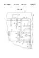
- FIG. 2Ashows a bottom fragmentary view of a flexible substrate used in the compliant multichip package shown in FIG. 1 in accordance with one preferred embodiment of the present invention.
- FIG. 2Bshows a close-up view of a portion of the flexible substrate shown in FIG. 2A.
- FIG. 3shows a side view of the compliant multichip package shown in FIG. 1 during further stages of an assembly process.
- FIG. 4shows the package of FIG. 3 during further stages of an assembly process.
- FIG. 5shows a bottom fragmentary view of the flexible substrate shown in FIG. 1 according to yet another preferred embodiment of the present invention.
- FIG. 6shows an exploded side view of a compliant multichip package according to another embodiment of the present invention.
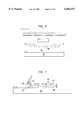
- FIG. 7shows the compliant multichip package shown in FIG. 6 during one stage of an assembly process
- FIG. 8shows a side view of the compliant multichip package shown in FIG. 6 during further stages of an assembly process according to preferred embodiments of the present invention.
- FIG. 9shows a side view of the package shown in FIG. 8 during further stages of an assembly process according to preferred methods of the present invention.
- FIG. 10shows a side view of the package shown in FIG. 9 during further stages of an assembly process according to preferred embodiments of the present invention.
- FIG. 11shows a fragmentary side view of a plurality of compliant pads used during assembly of a compliant multichip package according to further preferred embodiments of the present invention.
- FIG. 12shows a fragmentary side view of the compliant pads shown in FIG. 11 during further stages of an assembly process according to preferred embodiments of the present invention.
- FIG. 13shows a fragmentary side view of a compliant multichip package according to yet another preferred embodiment of the present invention.
- FIG. 14shows close-up fragmentary side view of the compliant multichip package shown in FIG. 13.
- FIG. 15shows a side view of a compliant multichip package according to yet another preferred embodiment of the present invention.
- FIG. 16shows a side view of a compliant multichip package according to still another preferred embodiment of the present invention.
- FIG. 17shows a fragmentary top view of the package shown in FIG. 16 during one stage of an assembly process.
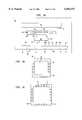
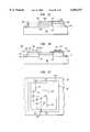
- one embodiment of the present inventionprovides a method of making a compliant multichip package 20 which includes providing a flexible substrate 22 having a top surface 24 and a bottom surface 26.
- the flexible substrate 22preferably includes a sheet-like dielectric film of the type used in tape automated bonding ("TAB") processes.
- TABtape automated bonding
- the flexible substrate 22is provided with sprocket holes 28 to facilitate feeding and movement of the flexible substrate 22 during various assembly processes.
- the flexible substrateis preferably about 0.01 to about 0.1 millimeters thick.
- top and bottomare used herein to indicate directions relative to the structure of the compliant multichip package itself.
- the flexible substrate 22has an interior bond window 30 and an exterior bond window 32.
- the interior bond window 30 and the exterior bond window 32include gaps in the form of elongated channels which extend through the flexible substrate 22 from the top surface 24 to the bottom surface 26 thereof.
- the interior bond window 30includes two channels which are substantially parallel to one another; however, the interior bond window may have more or less than two substantially parallel channels depending on the chip or microelectronic component selected for attachment to the flexible substrate 22.
- the exterior bond window 32includes gaps which are contiguous with one another to form a square or ring-shaped bond window.
- the flexible substrate 22includes an inner region 34 and a peripheral region 36 which surrounds the inner region 34, the exterior bond window 32 lying between the inner region 34 and the peripheral region 36.
- the inner region 34 of the flexible substrate 22also includes a central region 37 which is bounded and defined by the interior bond window 30.
- the flexible substrate 22includes a plurality of conductive traces 38 having outer ends 40 extending toward the peripheral region 36 of the flexible substrate and inner ends 41 extending toward the central region 37 of the flexible substrate.
- the conductive traces 38are desirably photolithographically defined from a single sheet of copper attached, such as by lamination, electroplating or sputtering processes, to the top surface 24 of the flexible substrate 22.
- the substrateincludes flexible leads 42A connected to outer ends 40 of the conductive traces 38.
- the flexible leads 42A at the outer ends 40 of the conductive traces 38extend at least partially across the exterior bond window 32.
- the inner region 34 of the flexible substrate 22is temporarily connected to the peripheral region 36 of the flexible substrate 22 by the flexible leads which extend across the exterior bond window 32.
- the flexible leads 42A connected to the outer ends 40 of the conductive traces 38are preferably configured to be detachable from the peripheral region of flexible substrate 22. Detachable lead structures are described in commonly assigned U.S. Pat. Nos. 5,489,749 and 5,536,909, the disclosures of which are hereby incorporated by reference herein.
- Flexible leads 42B connected to the inner ends 41 of the conductive traces 38extend at least partially across the interior bond window 30. Leads 42B may be detachably secured to the central region 37, or else may be permanently secured on both sides of the slot or interior bond window 30.
- the flexible substrate 22includes conductive terminals 44 accessible at the bottom surface 26 thereof which are connected to at least some of the conductive traces 38.
- a first microelectronic element 50preferably a relatively small semiconductor chip such as a memory chip, has a front face 52 including contacts 54 and a rear surface 56.
- the first microelectronic element 50has a central region 58 and a peripheral region 60 surrounding the central region 58 with the contacts 54 on the front face 52 thereof being disposed in the peripheral region 60.
- the first microelectronic element 50is assembled with the flexible substrate 22 so that the central portion 58 thereof is abutted against the central region 37 of the flexible substrate 22, with the contacts 54 aligned with the interior bond window 30.
- Alignment of the contacts 54 with the interior bond window 30facilitates bonding of the flexible leads 42B at the inner ends 41 of conductive traces 38 with the contacts 54 of the first microelectronic element 50.
- a bonding tape or adhesivemay be provided between the flexible substrate 22 and the first microelectronic element 50 using standard lamination or screen printing techniques to form a strong bond between the first microelectronic element 50 and the flexible substrate 22.
- the flexible leads 42B at the inner ends 41 of the conductive traces 38are then bonded to the contacts 54 on the front face 52 of the first microelectronic element 50, such as by using an ultrasonic or thermosonic bonding technique conventionally known in the art or by using the various bonding techniques disclosed in U.S. Pat. Nos. 5,398,863; 5,390,844; 5,536,909 and 5,491,302.
- a pre-formed compliant element 58such as a compliant silicone elastomer material, is then deposited over the rear surface 56 of the first microelectronic element 50 so that the compliant element 58 completely covers the edges 60 and the rear surface 56 of the first microelectronic element 50.
- the compliant element 58preferably includes a substantially continuous compliant pad having a pre-formed, cut-out region 62 or indentation having dimensions substantially similar to the external dimensions of the edges 60 and rear surface 56 of the first microelectronic element 50.
- the compliant elementincludes a relatively thick, rectangular ring-like structure 59 surrounding indentation 62, and a relatively thin compliant layer 61 forming a floor at the rear surface of the indentation.
- the cut-out region 62intimately surrounds and engages the edges 60 and rear surface 56 of the first microelectronic element 50.
- a second microelectronic element 64which typically is a relatively large semiconductor chip such as a microprocessor, a microcontroller or an ASIC, is then provided over a rear surface 66 of the compliant element 58 remote from the rear surface 56 of the first microelectronic element 50.
- the second microelectronic element 64is larger in size than the first microelectronic element 50.
- the second microelectronic element 64desirably includes a front face 68 having a central portion 70, a peripheral portion 72 which surrounds the central portion 70 and contacts 74 disposed in the peripheral portion 72.
- the second microelectronic element 64is assembled with the compliant element 58 so that the central portion 70 thereof is abutted against the rear surface 66 of the compliant element 58.
- the front face 68 of second microelectronic element 64faces toward the first microelectronic element 50 and the substrate 22.
- Compliant layer 61is disposed between the confronting faces of the microelectronic elements, whereas the ring-like structure 59 extends alongside of the first microelectronic element in the space between the second microelectronic element and substrate 22.
- the second microelectronic element 64after the second microelectronic element 64 has been assembled to the compliant element 58, the second microelectronic element 64 overlies the first microelectronic element 50 and the flexible substrate 22, with the contacts 74 of the second microelectronic element 64 aligned with the exterior bond window 32.
- the flexible leads 42A at the outer ends 40 of the conductive traces 38are then connected to the contacts 74 of the second microelectronic element 64.
- flexible leads 42Aare bent downwardly to the vertically-extensive configuration depicted in FIG. 3. In this configuration, leads 42A extend alongside the outer edges of the compliant element 58.
- traces 38electrically interconnect the first and second microelectronic elements 50 and 64 with one another. Connection of flexible leads 42A to the second microelectronic element 64 also serves to connect the second microelectronic element to terminals 44. Only some of the conductive traces 38 are connected to the conductive terminals 44. For example, the conductive trace 38A shown on the left side of FIG. 3A interconnects the first and second microelectronic elements 50 and 64 with one another and with the conductive terminal 44. The conductive trace 38B on the right side of FIG. 3A interconnects the first and second microelectronic elements 50 and 64 with one another, however, it is not connected to a conductive terminal. Also, only some of the conductive traces 38 interconnect the first and second microelectronic elements. Thus, trace 38C connects the second microelectronic element to a terminal 44, but does not make connection with the first microelectronic element 50.
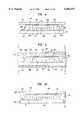
- a curable liquid encapsulant 76such as a liquid silicone elastomer, is then introduced between the second microelectronic element 64 and the first surface 24 of the flexible substrate 22.
- a protective coverlay 78such as that disclosed in commonly assigned U.S. Provisional Patent Application Ser. No. 60/032,871 filed Dec. 13, 1996, the disclosure of which is incorporated herein by reference, is provided over the bottom surface 26 of the flexible substrate 22 to cover the interior and exterior bond windows 30 and 32. The coverlay, prevents the liquid encapsulant from flowing through the bond windows and contacting the terminals 44 at the bottom surface 26 of the flexible substrate 22.
- the curable liquid encapsulant 76is then cured to form a compliant material, using energy such as heat or ultraviolet light.
- the compliant material formed from the cured encapsulantmerges with the compliant material of the original compliant element 58 to form a larger compliant element encompassing the first and second microelectronic elements and flexible leads 42A.
- the finished packagecan be handled, stored and shipped as a unit. It can be connected to a circuit panel (not shown) by bonding terminals 44 to contact pads on the circuit panel, as by solder bonding the terminals to the contact pads.
- FIG. 5shows a flexible substrate 222 according to yet another embodiment which includes conductive terminals 244B which are accessible at the central region 237 of the flexible substrate and which are connected to conductive traces 238 running to the interior bond window 230.
- the flexible substratealso includes conductive terminals 244A which are accessible at the inner region 236 of the flexible substrate 222 and which are connected to conductive traces extending toward the exterior bond window 232 or which extend between the exterior bond window 232 and the interior bond window 230.
- Substrate 222can be used in the same manner as the substrate discussed above with reference to FIGS. 1-4.
- the compliant elementin another embodiment of the present invention includes a plurality of central compliant pads 358 which are provided over the central region of front face 368 of the second microelectronic element 364.
- the compliant elementalso includes a plurality of peripheral compliant pads 371 provided over the peripheral region of the second microelectronic element.
- a stencil 380having a top surface 382 and a bottom surface 384 with a plurality of apertures 386 formed therein is provided over the central region of front face 368 of the second microelectronic element 364 so that the bottom surface 384 of the stencil mask 380 abuts against the front face 368 of the second microelectronic element 364.
- a curable liquid material 388such as a curable silicone elastomer, is then screened or stenciled printed across the top surface 382 of the stencil mask 380 so that the silicone elastomer 388 fills the apertures 386.
- the stencil mask 380is then removed from engagement with the front face 368 of the second microelectronic element 364.
- the uncured silicone elastomer pads 358remain on the front face 368 of the second microelectronic element 364.
- Peripheral compliant pads 371are formed using a similar stencil (not shown) overlying the peripheral region of the microelectronic element.
- the compliant pads 358 and 371preferably are only partially cured, so that they have sufficient rigidity to remain in place but still remain tacky. The cure is not completed until later stages of the assembly process.
- the rear face 356 of the first microelectronic element 350is then abutted against surfaces of the compliant pads 358 which are remote from the front face 368 of the second microelectronic element 364.
- the flexible substrate 322is then assembled with the first and second microelectronic elements 350 and 364 so that the interior bond window 330 is aligned with the contacts 354 of the first microelectronic element 350 and the exterior bond window 332 is aligned with the contacts 374 of the second microelectronic element 364.
- the peripheral region of substrate 322is supported by the peripheral compliant pads 371.
- the first and second microelectronic elements 350 and 360are then electrically interconnected with one another and with at least some of the conductive terminals 344 using the bonding techniques described above.
- the pad assembly process described abovemay be reversed.
- the first microelectronic element 350is assembled with the flexible substrate 322 and the compliant pads 358 are assembled with the rear surface 356 of the first microelectronic element 350.
- Peripheral pads 371are assembled to the peripheral region of the substrate.
- the second microelectronic elementis then assembled with the compliant pads 358 and 371, and the first and second microelectronic elements 350 and 364 are then interconnected with one another and with at least some of the conductive terminals 344.
- a curable liquid encapsulant 376is introduced between the second microelectronic element 364 and the flexible substrate 322 in accordance with the methods described in U.S. Pat. No. 5,659,952, the disclosure of which is hereby incorporated by reference herein.
- a protective coverlay 392Asuch as that disclosed in copending, commonly assigned U.S. patent application Ser. No.
- 08/726,697is provided over the second surface 326 of the flexible substrate 322 to prevent the curable liquid encapsulant 376 from flowing through the interior and exterior bond windows 330 and 332 and contacting the conductive terminals 344 accessible at the second surface 326 of the flexible substrate 322.
- a second protective coverlay 392Bmay be provided over the rear surface 394 of the second microelectronic element 364. After the liquid encapsulant 376 is introduced, it surrounds the conductive traces 338 and passes through the channels 390 between the compliant pads 358 and 371. The encapsulant is then cured using energy such as heat or ultraviolet light.
- the encapsulant 376is preferably CTE matched with the compliant pads 358 and 371 so that the pads and the encapsulant form a uniform compliant element between the second microelectronic element 364 and the flexible substrate 322.
- the protective coverlays 392A and 392Bmay be removed after the curable liquid encapsulant 376 has been cured or may remain in place while the package is in storage to protect the package and the conductive terminals 344 from contamination.
- the outer portion of the compliant element formed by encapsulant 376may then be severed outside the periphery of the second microelectronic element 364, along the axis designated A--A, to provide an individual compliant multichip packages of precise size.
- the encapsulant layer 376extends beyond the perimeter of the second microelectronic element to provide resilient bumpers 390 around the perimeter of the package.
- the plurality of compliant pads 458 described abovemay be transferable, such as those disclosed in U.S. patent application Ser. No. 08/879,922, the disclosure of which is incorporated by reference herein.
- the plurality of compliant pads 458are initially stored separately from the other package elements, between a first storage liner 494 and a second storage liner 496.
- the first and second storage liners 494 and 496include a tacky material 498, such as an adhesive, which provides tack to the top and bottom surfaces of the compliant pads 458.
- the tacky material 498may be an adhesive such as a pressure sensitive adhesive or other known adhesive for providing the surface regions of the compliant pads 458 with tack.
- the first storage liner 494is peeled away from the plurality of compliant pads 458 to expose the bottom surfaces of the compliant pads.
- heatmay be applied to the exterior surface of the first liner 494 to reduce the level of tack between the first liner 494 and the compliant pads 458 to thereby ensure that the compliant pads 458 will remain attached to the second liner 496 until it is desirable to remove the second liner 496.
- the first liner 494should preferably be pulled at a severe angle which further ensures that the compliant pads 458 remain attached to the second storage liner 496.
- the compliant pads 458are assembled to the front face 468 of the second microelectronic element 464.
- the second storage liner 496is then removed from the compliant pads 458 to expose the top surface region thereof and the rear surface of the first microelectronic element (not shown) is preferably abutted against the top surface of the compliant pads 458.
- the flexible substrateis then assembled with the first microelectronic element as described above with reference to FIGS. 8-10.
- Peripheral compliant pads(not shown) are provided by a similar process. In other preferred embodiments the transferable compliant pads are first assembled with the rear surface of the first microelectronic element and with the peripheral portion of the substrate.
- the inner ends 541 of the conductive traces 538 which extend to the interior bond window 530are releasably attached to the flexible substrate 522.
- the inner ends 541 of the conductive traces 538bridge the bond windows 530.
- the inner ends 541are bonded to the contacts 554 of the first microelectronic element by advancing a thermosonic, ultrasonic or other similar bonding tool into the bond window to form permanent bonds 595 between the lead ends and the contacts 554.
- the bonds 595are depicted in FIGS. 13 and 14 as having some downward bending relative to the rest of the conductive traces, this is not essential.
- the inner ends of the tracesneed not be flexible.
- Rigid connections between the inner ends of the traces and the first microelectronic elementdo not provide for mechanical decoupling of the first microelectronic element and the substrate.
- the stresses created during operation by differential thermal expansion and warpage of the first microelectronic elementare also relatively small. Therefore, the absence of mechanical decoupling can be tolerated at these connections.
- the outer ends of the leads, which are connected to the larger, second microelectronic elementshould be flexible to accommodate the larger relative motion of the contacts on the second microelectronic element. Stated another way, mechanical decoupling of the second microelectronic element from the substrate is more important than mechanical decoupling of the first microelectronic element from the substrate.
- the flexible substrate 722includes an interior bond window 730 which is a unitary central aperture extending between the top and bottom surface thereof. In this embodiment, the central region of the substrate inside of the interior bond window used in the embodiments discussed above is omitted.
- the conductive traces 738extend across the first surface 724 of the flexible substrate 722.
- the inner ends 741 of the conductive traces 738include flexible leads 742 which are cantilevered over the central aperture.
- the flexible leads 742 at the inner ends 741 of the conductive traces 738are connected to the contacts 754 of the first microelectronic element 750 through conventional tape automated bonding techniques.
- the flexible leads 742 at the outer ends 740 of the conductive traces 738are connected to the contacts 774 of the second microelectronic element 764 in a substantially similar manner.
- the conductive traces 738are electrically connected to the conductive terminals 744 through conductive vias 797 extending through the flexible substrate 722.
- the flexible leads 742 at the inner and outer ends of the conductive traces 738are preferably encapsulated using the curable liquid encapsulant processes described above.
- the encapsulant(not shown) is then cured to provide a compliant layer for the package 720.
- the multichip packagesmay include the first and second microelectronic elements provided one atop the other with additional microelectronic elements provided to the side(s) of the first and second microelectronic elements.
- the additional microelectronic elements provided to the side(s)are also disposed within the package.
- the packagemay include additional packaging elements such as a metallic heat sink or protective cover overlying the rear surface of the second microelectronic element and preferably surrounding the other components.
- a plurality of the above-described multichip packagesare provided side-by-side so that the packages may be simultaneously encapsulated to provide a unitary compliant element extending into several packages.
- the unitary compliant elementis then severed to separate the packages from one another.
- the second microelectronic elementsmay be chips constituting parts of a wafer, and the remaining process steps may be performed before severing the chips from one another while also severing the unitary compliant element.
Landscapes
- Engineering & Computer Science (AREA)
- Microelectronics & Electronic Packaging (AREA)
- Power Engineering (AREA)
- Computer Hardware Design (AREA)
- Physics & Mathematics (AREA)
- Condensed Matter Physics & Semiconductors (AREA)
- General Physics & Mathematics (AREA)
- Manufacturing & Machinery (AREA)
- Wire Bonding (AREA)
- Structure Of Printed Boards (AREA)
Abstract
Description
Claims (39)
Priority Applications (3)
| Application Number | Priority Date | Filing Date | Title |
|---|---|---|---|
| US08/989,710US6054337A (en) | 1996-12-13 | 1997-12-12 | Method of making a compliant multichip package |
| US09/500,364US6147401A (en) | 1996-12-13 | 2000-02-08 | Compliant multichip package |
| US09/632,986US6313528B1 (en) | 1996-12-13 | 2000-08-04 | Compliant multichip package |
Applications Claiming Priority (2)
| Application Number | Priority Date | Filing Date | Title |
|---|---|---|---|
| US3335296P | 1996-12-13 | 1996-12-13 | |
| US08/989,710US6054337A (en) | 1996-12-13 | 1997-12-12 | Method of making a compliant multichip package |
Related Child Applications (1)
| Application Number | Title | Priority Date | Filing Date |
|---|---|---|---|
| US09/500,364DivisionUS6147401A (en) | 1996-12-13 | 2000-02-08 | Compliant multichip package |
Publications (1)
| Publication Number | Publication Date |
|---|---|
| US6054337Atrue US6054337A (en) | 2000-04-25 |
Family
ID=26709596
Family Applications (3)
| Application Number | Title | Priority Date | Filing Date |
|---|---|---|---|
| US08/989,710Expired - LifetimeUS6054337A (en) | 1996-12-13 | 1997-12-12 | Method of making a compliant multichip package |
| US09/500,364Expired - LifetimeUS6147401A (en) | 1996-12-13 | 2000-02-08 | Compliant multichip package |
| US09/632,986Expired - LifetimeUS6313528B1 (en) | 1996-12-13 | 2000-08-04 | Compliant multichip package |
Family Applications After (2)
| Application Number | Title | Priority Date | Filing Date |
|---|---|---|---|
| US09/500,364Expired - LifetimeUS6147401A (en) | 1996-12-13 | 2000-02-08 | Compliant multichip package |
| US09/632,986Expired - LifetimeUS6313528B1 (en) | 1996-12-13 | 2000-08-04 | Compliant multichip package |
Country Status (1)
| Country | Link |
|---|---|
| US (3) | US6054337A (en) |
Cited By (95)
| Publication number | Priority date | Publication date | Assignee | Title |
|---|---|---|---|---|
| US6236109B1 (en)* | 1999-01-29 | 2001-05-22 | United Microelectronics Corp. | Multi-chip chip scale package |
| US6291259B1 (en)* | 1998-05-30 | 2001-09-18 | Hyundai Electronics Industries Co., Ltd. | Stackable ball grid array semiconductor package and fabrication method thereof |
| US6294040B1 (en)* | 1996-12-13 | 2001-09-25 | Tessera, Inc. | Transferable resilient element for packaging of a semiconductor chip and method therefor |
| US6307749B1 (en)* | 2000-10-23 | 2001-10-23 | Delphi Technologies, Inc. | Overmolded electronic module with underfilled surface-mount components |
| US6324072B1 (en)* | 1996-09-30 | 2001-11-27 | Siemens Aktiengesellschaft | Microelectronic component of sandwich construction |
| US6482673B2 (en)* | 1996-10-17 | 2002-11-19 | Seiko Epson Corporation | Semiconductor device, method of making the same, circuit board, flexible substrate, and method of making substrate |
| US20020180035A1 (en)* | 2001-06-04 | 2002-12-05 | Siliconware Precision Industries Co., Ltd. | Semiconductor package with heat sink |
| US6515370B2 (en)* | 1997-03-10 | 2003-02-04 | Seiko Epson Corporation | Electronic component and semiconductor device, method for manufacturing the same, circuit board have the same mounted thereon, and electronic equipment having the circuit board |
| US20030038356A1 (en)* | 2001-08-24 | 2003-02-27 | Derderian James M | Semiconductor devices including stacking spacers thereon, assemblies including the semiconductor devices, and methods |
| US20030048624A1 (en)* | 2001-08-22 | 2003-03-13 | Tessera, Inc. | Low-height multi-component assemblies |
| US6602737B2 (en)* | 2001-04-18 | 2003-08-05 | Siliconware Precision Industries Co., Ltd. | Semiconductor package with heat-dissipating structure and method of making the same |
| US6651868B2 (en)* | 2001-01-19 | 2003-11-25 | Kabushiki Kaisha Shinkawa | Workpiece retainer for a bonding apparatus |
| US6791171B2 (en) | 2000-06-20 | 2004-09-14 | Nanonexus, Inc. | Systems for testing and packaging integrated circuits |
| US20040262729A1 (en)* | 2003-06-30 | 2004-12-30 | Takashi Kumamoto | Microelectronic package array |
| US20050017345A1 (en)* | 2001-06-27 | 2005-01-27 | Intel Corporation | Flexible tape electronics packaging and methods of manufacture |
| US20050026476A1 (en)* | 2000-06-20 | 2005-02-03 | Sammy Mok | Systems for testing and packaging integrated circuits |
| US20050056922A1 (en)* | 2003-08-29 | 2005-03-17 | Vasoya Kalu K. | Expansion constrained die stack |
| US20050277228A1 (en)* | 2004-06-14 | 2005-12-15 | David Lee | Method and apparatus for forming interposers on integrated circuits |
| US20050280134A1 (en)* | 2004-06-18 | 2005-12-22 | Tessera, Inc. | Multi-frequency noise suppression capacitor set |
| DE102004055061A1 (en)* | 2004-11-15 | 2006-05-18 | Robert Bosch Gmbh | Method for arranging a flip-chip on a substrate |
| US20060186906A1 (en)* | 2000-05-23 | 2006-08-24 | Bottoms W R | High density interconnect system for IC packages and interconnect assemblies |
| US20060258052A1 (en)* | 2000-02-16 | 2006-11-16 | Micron Technology, Inc. | Wafer level pre-packaged flip chip |
| US20070024128A1 (en)* | 2005-08-01 | 2007-02-01 | Denso Corporation | Vehicle-use generator |
| US20070057684A1 (en)* | 1999-05-27 | 2007-03-15 | Chong Fu C | Massively parallel interface for electronic circuit |
| US20070098895A1 (en)* | 2001-08-24 | 2007-05-03 | Smith Donald L | Method and Apparatus for Producing Uniform, Isotropic Stresses in a Sputtered Film |
| US20070164412A1 (en)* | 2002-10-15 | 2007-07-19 | Megica Corporation | Method of wire bonding over active area of a semiconductor circuit |
| US20070232053A1 (en)* | 2002-10-24 | 2007-10-04 | Megica Corporation | Method for fabricating thermal compliant semiconductor chip wiring structure for chip scale packaging |
| US20070245553A1 (en)* | 1999-05-27 | 2007-10-25 | Chong Fu C | Fine pitch microfabricated spring contact structure & method |
| US20080011507A1 (en)* | 2006-07-14 | 2008-01-17 | Vasoya Kalu K | Build-up printed wiring board substrate having a core layer that is part of a circuit |
| US20080054429A1 (en)* | 2006-08-25 | 2008-03-06 | Bolken Todd O | Spacers for separating components of semiconductor device assemblies, semiconductor device assemblies and systems including spacers and methods of making spacers |
| US7349223B2 (en) | 2000-05-23 | 2008-03-25 | Nanonexus, Inc. | Enhanced compliant probe card systems having improved planarity |
| US7382142B2 (en) | 2000-05-23 | 2008-06-03 | Nanonexus, Inc. | High density interconnect system having rapid fabrication cycle |
| US20090057901A1 (en)* | 2001-09-17 | 2009-03-05 | Megica Corporation | Structure of high performance combo chip and processing method |
| US20090057919A1 (en)* | 2000-05-19 | 2009-03-05 | Megica Corporation | Multiple chips bonded to packaging structure with low noise and multiple selectable functions |
| US20090278255A1 (en)* | 2008-05-09 | 2009-11-12 | Kouji Oomori | Semiconductor device |
| US7952373B2 (en) | 2000-05-23 | 2011-05-31 | Verigy (Singapore) Pte. Ltd. | Construction structures and manufacturing processes for integrated circuit wafer probe card assemblies |
| US8168527B2 (en) | 2006-09-06 | 2012-05-01 | Megica Corporation | Semiconductor chip and method for fabricating the same |
| US8426982B2 (en) | 2001-03-30 | 2013-04-23 | Megica Corporation | Structure and manufacturing method of chip scale package |
| US8618659B2 (en) | 2011-05-03 | 2013-12-31 | Tessera, Inc. | Package-on-package assembly with wire bonds to encapsulation surface |
| US8623706B2 (en)* | 2010-11-15 | 2014-01-07 | Tessera, Inc. | Microelectronic package with terminals on dielectric mass |
| US20140138809A1 (en)* | 2012-11-20 | 2014-05-22 | Raydium Semiconductor Corporation | Package structure and manufacturing method thereof |
| US8772152B2 (en) | 2012-02-24 | 2014-07-08 | Invensas Corporation | Method for package-on-package assembly with wire bonds to encapsulation surface |
| US20140230989A1 (en)* | 2011-10-15 | 2014-08-21 | Danfoss Silicon Power Gmbh | Method for creating a connection between metallic moulded bodies and a power semiconductor which is used to bond to thick wires or strips |
| US8836136B2 (en) | 2011-10-17 | 2014-09-16 | Invensas Corporation | Package-on-package assembly with wire bond vias |
| US8835228B2 (en) | 2012-05-22 | 2014-09-16 | Invensas Corporation | Substrate-less stackable package with wire-bond interconnect |
| US8878353B2 (en) | 2012-12-20 | 2014-11-04 | Invensas Corporation | Structure for microelectronic packaging with bond elements to encapsulation surface |
| US8883563B1 (en) | 2013-07-15 | 2014-11-11 | Invensas Corporation | Fabrication of microelectronic assemblies having stack terminals coupled by connectors extending through encapsulation |
| US8907466B2 (en) | 2010-07-19 | 2014-12-09 | Tessera, Inc. | Stackable molded microelectronic packages |
| US8927337B2 (en) | 2004-11-03 | 2015-01-06 | Tessera, Inc. | Stacked packaging improvements |
| US8975738B2 (en) | 2012-11-12 | 2015-03-10 | Invensas Corporation | Structure for microelectronic packaging with terminals on dielectric mass |
| US9023691B2 (en) | 2013-07-15 | 2015-05-05 | Invensas Corporation | Microelectronic assemblies with stack terminals coupled by connectors extending through encapsulation |
| US9034696B2 (en) | 2013-07-15 | 2015-05-19 | Invensas Corporation | Microelectronic assemblies having reinforcing collars on connectors extending through encapsulation |
| US9082753B2 (en) | 2013-11-12 | 2015-07-14 | Invensas Corporation | Severing bond wire by kinking and twisting |
| US9087815B2 (en) | 2013-11-12 | 2015-07-21 | Invensas Corporation | Off substrate kinking of bond wire |
| USRE45637E1 (en) | 2005-08-29 | 2015-07-28 | Stablcor Technology, Inc. | Processes for manufacturing printed wiring boards |
| US9159708B2 (en) | 2010-07-19 | 2015-10-13 | Tessera, Inc. | Stackable molded microelectronic packages with area array unit connectors |
| US9214454B2 (en) | 2014-03-31 | 2015-12-15 | Invensas Corporation | Batch process fabrication of package-on-package microelectronic assemblies |
| US9218988B2 (en) | 2005-12-23 | 2015-12-22 | Tessera, Inc. | Microelectronic packages and methods therefor |
| US9224717B2 (en) | 2011-05-03 | 2015-12-29 | Tessera, Inc. | Package-on-package assembly with wire bonds to encapsulation surface |
| US9324681B2 (en) | 2010-12-13 | 2016-04-26 | Tessera, Inc. | Pin attachment |
| US9332632B2 (en) | 2014-08-20 | 2016-05-03 | Stablcor Technology, Inc. | Graphene-based thermal management cores and systems and methods for constructing printed wiring boards |
| US9349706B2 (en) | 2012-02-24 | 2016-05-24 | Invensas Corporation | Method for package-on-package assembly with wire bonds to encapsulation surface |
| US9391008B2 (en) | 2012-07-31 | 2016-07-12 | Invensas Corporation | Reconstituted wafer-level package DRAM |
| US20160225738A1 (en)* | 2011-10-15 | 2016-08-04 | Danfoss Silicon Power Gmbh | Power semiconductor chip with a metallic moulded body for contacting thick wires or strips and method for the production thereof |
| US9412714B2 (en) | 2014-05-30 | 2016-08-09 | Invensas Corporation | Wire bond support structure and microelectronic package including wire bonds therefrom |
| US9502390B2 (en) | 2012-08-03 | 2016-11-22 | Invensas Corporation | BVA interposer |
| US9530749B2 (en) | 2015-04-28 | 2016-12-27 | Invensas Corporation | Coupling of side surface contacts to a circuit platform |
| US9583411B2 (en) | 2014-01-17 | 2017-02-28 | Invensas Corporation | Fine pitch BVA using reconstituted wafer with area array accessible for testing |
| US9601454B2 (en) | 2013-02-01 | 2017-03-21 | Invensas Corporation | Method of forming a component having wire bonds and a stiffening layer |
| US9646917B2 (en) | 2014-05-29 | 2017-05-09 | Invensas Corporation | Low CTE component with wire bond interconnects |
| US9659848B1 (en) | 2015-11-18 | 2017-05-23 | Invensas Corporation | Stiffened wires for offset BVA |
| US9685365B2 (en) | 2013-08-08 | 2017-06-20 | Invensas Corporation | Method of forming a wire bond having a free end |
| US9728527B2 (en) | 2013-11-22 | 2017-08-08 | Invensas Corporation | Multiple bond via arrays of different wire heights on a same substrate |
| US9735084B2 (en) | 2014-12-11 | 2017-08-15 | Invensas Corporation | Bond via array for thermal conductivity |
| US9761554B2 (en) | 2015-05-07 | 2017-09-12 | Invensas Corporation | Ball bonding metal wire bond wires to metal pads |
| US9812402B2 (en) | 2015-10-12 | 2017-11-07 | Invensas Corporation | Wire bond wires for interference shielding |
| US9842745B2 (en) | 2012-02-17 | 2017-12-12 | Invensas Corporation | Heat spreading substrate with embedded interconnects |
| US9852969B2 (en) | 2013-11-22 | 2017-12-26 | Invensas Corporation | Die stacks with one or more bond via arrays of wire bond wires and with one or more arrays of bump interconnects |
| US9888579B2 (en) | 2015-03-05 | 2018-02-06 | Invensas Corporation | Pressing of wire bond wire tips to provide bent-over tips |
| US9911718B2 (en) | 2015-11-17 | 2018-03-06 | Invensas Corporation | ‘RDL-First’ packaged microelectronic device for a package-on-package device |
| US9935075B2 (en) | 2016-07-29 | 2018-04-03 | Invensas Corporation | Wire bonding method and apparatus for electromagnetic interference shielding |
| US9984992B2 (en) | 2015-12-30 | 2018-05-29 | Invensas Corporation | Embedded wire bond wires for vertical integration with separate surface mount and wire bond mounting surfaces |
| US10008477B2 (en) | 2013-09-16 | 2018-06-26 | Invensas Corporation | Microelectronic element with bond elements to encapsulation surface |
| US10008469B2 (en) | 2015-04-30 | 2018-06-26 | Invensas Corporation | Wafer-level packaging using wire bond wires in place of a redistribution layer |
| US10026717B2 (en) | 2013-11-22 | 2018-07-17 | Invensas Corporation | Multiple bond via arrays of different wire heights on a same substrate |
| US10181457B2 (en) | 2015-10-26 | 2019-01-15 | Invensas Corporation | Microelectronic package for wafer-level chip scale packaging with fan-out |
| US10192845B2 (en)* | 2014-07-07 | 2019-01-29 | Rohm Co., Ltd. | Electronic device and mounting structure of the same |
| US10299368B2 (en) | 2016-12-21 | 2019-05-21 | Invensas Corporation | Surface integrated waveguides and circuit structures therefor |
| US10332854B2 (en) | 2015-10-23 | 2019-06-25 | Invensas Corporation | Anchoring structure of fine pitch bva |
| US20190198452A1 (en)* | 2017-12-27 | 2019-06-27 | Toshiba Memory Corporation | Semiconductor device |
| US10381326B2 (en) | 2014-05-28 | 2019-08-13 | Invensas Corporation | Structure and method for integrated circuits packaging with increased density |
| US10460958B2 (en) | 2013-08-07 | 2019-10-29 | Invensas Corporation | Method of manufacturing embedded packaging with preformed vias |
| US10490528B2 (en) | 2015-10-12 | 2019-11-26 | Invensas Corporation | Embedded wire bond wires |
| US20210407911A1 (en)* | 2020-06-29 | 2021-12-30 | Samsung Electronics Co., Ltd. | Semiconductor package and a package-on-package including the same |
| US20230230966A1 (en)* | 2022-01-14 | 2023-07-20 | Advanced Semiconductor Engineering, Inc. | Electronic package and electronic device |
Families Citing this family (98)
| Publication number | Priority date | Publication date | Assignee | Title |
|---|---|---|---|---|
| US6870272B2 (en)* | 1994-09-20 | 2005-03-22 | Tessera, Inc. | Methods of making microelectronic assemblies including compliant interfaces |
| US6284563B1 (en) | 1995-10-31 | 2001-09-04 | Tessera, Inc. | Method of making compliant microelectronic assemblies |
| US6211572B1 (en) | 1995-10-31 | 2001-04-03 | Tessera, Inc. | Semiconductor chip package with fan-in leads |
| US6054337A (en)* | 1996-12-13 | 2000-04-25 | Tessera, Inc. | Method of making a compliant multichip package |
| JPH10294423A (en)* | 1997-04-17 | 1998-11-04 | Nec Corp | Semiconductor device |
| US6914196B2 (en) | 1998-01-09 | 2005-07-05 | Samsung Electronics Co., Ltd. | Reel-deployed printed circuit board |
| KR100272737B1 (en)* | 1998-01-09 | 2001-01-15 | 윤종용 | reel printed circuit board and chip on board packages using the reel printed circuit board |
| SG75873A1 (en)* | 1998-09-01 | 2000-10-24 | Texas Instr Singapore Pte Ltd | Stacked flip-chip integrated circuit assemblage |
| JP2000223657A (en)* | 1999-02-03 | 2000-08-11 | Rohm Co Ltd | Semiconductor device and semiconductor chip used for the same |
| US6376915B1 (en)* | 1999-02-26 | 2002-04-23 | Rohm Co., Ltd | Semiconductor device and semiconductor chip |
| JP2003517709A (en) | 1999-12-17 | 2003-05-27 | オスラム オプト セミコンダクターズ ゲゼルシャフト ミット ベシュレンクテル ハフツング | Improved encapsulation for organic light emitting diode devices |
| US7394153B2 (en)* | 1999-12-17 | 2008-07-01 | Osram Opto Semiconductors Gmbh | Encapsulation of electronic devices |
| WO2001045140A2 (en) | 1999-12-17 | 2001-06-21 | Osram Opto Semiconductors Gmbh | Encapsulation for organic led device |
| JP3996315B2 (en)* | 2000-02-21 | 2007-10-24 | 松下電器産業株式会社 | Semiconductor device and manufacturing method thereof |
| US6448659B1 (en)* | 2000-04-26 | 2002-09-10 | Advanced Micro Devices, Inc. | Stacked die design with supporting O-ring |
| JP2001320014A (en)* | 2000-05-11 | 2001-11-16 | Seiko Epson Corp | Semiconductor device and manufacturing method thereof |
| JP2002040095A (en)* | 2000-07-26 | 2002-02-06 | Nec Corp | Semiconductor device and mounting method thereof |
| JP3565334B2 (en)* | 2001-01-25 | 2004-09-15 | シャープ株式会社 | Semiconductor device, liquid crystal module using the same, and method of manufacturing semiconductor device |
| US6472743B2 (en)* | 2001-02-22 | 2002-10-29 | Siliconware Precision Industries, Co., Ltd. | Semiconductor package with heat dissipating structure |
| DE10137666A1 (en)* | 2001-08-01 | 2003-02-27 | Infineon Technologies Ag | Protection device for assemblies and process for their manufacture |
| US7605479B2 (en)* | 2001-08-22 | 2009-10-20 | Tessera, Inc. | Stacked chip assembly with encapsulant layer |
| US7518223B2 (en)* | 2001-08-24 | 2009-04-14 | Micron Technology, Inc. | Semiconductor devices and semiconductor device assemblies including a nonconfluent spacer layer |
| US6509208B1 (en)* | 2001-09-14 | 2003-01-21 | Infineon Ag | Method for forming structures on a wafer |
| US6633005B2 (en) | 2001-10-22 | 2003-10-14 | Micro Mobio Corporation | Multilayer RF amplifier module |
| US6673698B1 (en) | 2002-01-19 | 2004-01-06 | Megic Corporation | Thin film semiconductor package utilizing a glass substrate with composite polymer/metal interconnect layers |
| TW503496B (en) | 2001-12-31 | 2002-09-21 | Megic Corp | Chip packaging structure and manufacturing process of the same |
| TW584950B (en) | 2001-12-31 | 2004-04-21 | Megic Corp | Chip packaging structure and process thereof |
| TW544882B (en) | 2001-12-31 | 2003-08-01 | Megic Corp | Chip package structure and process thereof |
| US6638870B2 (en)* | 2002-01-10 | 2003-10-28 | Infineon Technologies Ag | Forming a structure on a wafer |
| US20030218246A1 (en)* | 2002-05-22 | 2003-11-27 | Hirofumi Abe | Semiconductor device passing large electric current |
| US6677522B1 (en)* | 2002-09-26 | 2004-01-13 | International Business Machines Corporation | Package for electronic component |
| JP3867785B2 (en)* | 2002-10-15 | 2007-01-10 | セイコーエプソン株式会社 | Optical module |
| US7208825B2 (en)* | 2003-01-22 | 2007-04-24 | Siliconware Precision Industries Co., Ltd. | Stacked semiconductor packages |
| TWI235469B (en)* | 2003-02-07 | 2005-07-01 | Siliconware Precision Industries Co Ltd | Thermally enhanced semiconductor package with EMI shielding |
| KR100555507B1 (en)* | 2003-07-16 | 2006-03-03 | 삼성전자주식회사 | Thin Printed Circuit Boards for Chip Scale Package Manufacturing |
| US7294929B2 (en)* | 2003-12-30 | 2007-11-13 | Texas Instruments Incorporated | Solder ball pad structure |
| US7303941B1 (en) | 2004-03-12 | 2007-12-04 | Cisco Technology, Inc. | Methods and apparatus for providing a power signal to an area array package |
| US7116002B2 (en)* | 2004-05-10 | 2006-10-03 | Taiwan Semiconductor Manufacturing Company, Ltd. | Overhang support for a stacked semiconductor device, and method of forming thereof |
| US7588963B2 (en)* | 2004-06-30 | 2009-09-15 | Taiwan Semiconductor Manufacturing Company, Ltd. | Method of forming overhang support for a stacked semiconductor device |
| US7327044B2 (en)* | 2005-01-21 | 2008-02-05 | Fox Electronics | Integrated circuit package encapsulating a hermetically sealed device |
| CN101128931B (en)* | 2005-02-25 | 2010-05-19 | 德塞拉股份有限公司 | Microelectronic assemblies having compliancy |
| US7098073B1 (en) | 2005-04-18 | 2006-08-29 | Freescale Semiconductor, Inc. | Method for stacking an integrated circuit on another integrated circuit |
| US7196427B2 (en)* | 2005-04-18 | 2007-03-27 | Freescale Semiconductor, Inc. | Structure having an integrated circuit on another integrated circuit with an intervening bent adhesive element |
| US7304382B2 (en)* | 2006-01-11 | 2007-12-04 | Staktek Group L.P. | Managed memory component |
| US7710735B2 (en)* | 2006-04-01 | 2010-05-04 | Stats Chippac Ltd. | Multichip package system |
| US7633168B2 (en)* | 2006-06-28 | 2009-12-15 | Intel Corporation | Method, system, and apparatus for a secure bus on a printed circuit board |
| KR100912427B1 (en)* | 2006-10-23 | 2009-08-14 | 삼성전자주식회사 | Laminated chip package and its manufacturing method |
| US7749886B2 (en) | 2006-12-20 | 2010-07-06 | Tessera, Inc. | Microelectronic assemblies having compliancy and methods therefor |
| US7709951B2 (en)* | 2007-03-16 | 2010-05-04 | International Business Machines Corporation | Thermal pillow |
| FI122217B (en)* | 2008-07-22 | 2011-10-14 | Imbera Electronics Oy | Multi-chip package and manufacturing method |
| US7989950B2 (en)* | 2008-08-14 | 2011-08-02 | Stats Chippac Ltd. | Integrated circuit packaging system having a cavity |
| US9536815B2 (en) | 2009-05-28 | 2017-01-03 | Hsio Technologies, Llc | Semiconductor socket with direct selective metalization |
| US8955215B2 (en) | 2009-05-28 | 2015-02-17 | Hsio Technologies, Llc | High performance surface mount electrical interconnect |
| WO2010147939A1 (en) | 2009-06-17 | 2010-12-23 | Hsio Technologies, Llc | Semiconductor socket |
| WO2011153298A1 (en) | 2010-06-03 | 2011-12-08 | Hsio Technologies, Llc | Electrical connector insulator housing |
| US9276336B2 (en) | 2009-05-28 | 2016-03-01 | Hsio Technologies, Llc | Metalized pad to electrical contact interface |
| US9184145B2 (en) | 2009-06-02 | 2015-11-10 | Hsio Technologies, Llc | Semiconductor device package adapter |
| US9414500B2 (en) | 2009-06-02 | 2016-08-09 | Hsio Technologies, Llc | Compliant printed flexible circuit |
| US9320133B2 (en) | 2009-06-02 | 2016-04-19 | Hsio Technologies, Llc | Electrical interconnect IC device socket |
| US8988093B2 (en) | 2009-06-02 | 2015-03-24 | Hsio Technologies, Llc | Bumped semiconductor wafer or die level electrical interconnect |
| WO2010141296A1 (en) | 2009-06-02 | 2010-12-09 | Hsio Technologies, Llc | Compliant printed circuit semiconductor package |
| US8912812B2 (en) | 2009-06-02 | 2014-12-16 | Hsio Technologies, Llc | Compliant printed circuit wafer probe diagnostic tool |
| US9613841B2 (en) | 2009-06-02 | 2017-04-04 | Hsio Technologies, Llc | Area array semiconductor device package interconnect structure with optional package-to-package or flexible circuit to package connection |
| US9054097B2 (en) | 2009-06-02 | 2015-06-09 | Hsio Technologies, Llc | Compliant printed circuit area array semiconductor device package |
| WO2010141264A1 (en) | 2009-06-03 | 2010-12-09 | Hsio Technologies, Llc | Compliant wafer level probe assembly |
| US9232654B2 (en) | 2009-06-02 | 2016-01-05 | Hsio Technologies, Llc | High performance electrical circuit structure |
| US8610265B2 (en) | 2009-06-02 | 2013-12-17 | Hsio Technologies, Llc | Compliant core peripheral lead semiconductor test socket |
| WO2010141298A1 (en) | 2009-06-02 | 2010-12-09 | Hsio Technologies, Llc | Composite polymer-metal electrical contacts |
| US8525346B2 (en) | 2009-06-02 | 2013-09-03 | Hsio Technologies, Llc | Compliant conductive nano-particle electrical interconnect |
| US9699906B2 (en) | 2009-06-02 | 2017-07-04 | Hsio Technologies, Llc | Hybrid printed circuit assembly with low density main core and embedded high density circuit regions |
| US9136196B2 (en) | 2009-06-02 | 2015-09-15 | Hsio Technologies, Llc | Compliant printed circuit wafer level semiconductor package |
| WO2012074963A1 (en) | 2010-12-01 | 2012-06-07 | Hsio Technologies, Llc | High performance surface mount electrical interconnect |
| WO2010141318A1 (en) | 2009-06-02 | 2010-12-09 | Hsio Technologies, Llc | Compliant printed circuit peripheral lead semiconductor test socket |
| US9231328B2 (en) | 2009-06-02 | 2016-01-05 | Hsio Technologies, Llc | Resilient conductive electrical interconnect |
| US9603249B2 (en) | 2009-06-02 | 2017-03-21 | Hsio Technologies, Llc | Direct metalization of electrical circuit structures |
| WO2010141313A1 (en) | 2009-06-02 | 2010-12-09 | Hsio Technologies, Llc | Compliant printed circuit socket diagnostic tool |
| WO2011002709A1 (en) | 2009-06-29 | 2011-01-06 | Hsio Technologies, Llc | Compliant printed circuit semiconductor tester interface |
| US8955216B2 (en) | 2009-06-02 | 2015-02-17 | Hsio Technologies, Llc | Method of making a compliant printed circuit peripheral lead semiconductor package |
| US8987886B2 (en) | 2009-06-02 | 2015-03-24 | Hsio Technologies, Llc | Copper pillar full metal via electrical circuit structure |
| US9276339B2 (en) | 2009-06-02 | 2016-03-01 | Hsio Technologies, Llc | Electrical interconnect IC device socket |
| US9196980B2 (en) | 2009-06-02 | 2015-11-24 | Hsio Technologies, Llc | High performance surface mount electrical interconnect with external biased normal force loading |
| US9930775B2 (en) | 2009-06-02 | 2018-03-27 | Hsio Technologies, Llc | Copper pillar full metal via electrical circuit structure |
| US9318862B2 (en) | 2009-06-02 | 2016-04-19 | Hsio Technologies, Llc | Method of making an electronic interconnect |
| WO2010147934A1 (en) | 2009-06-16 | 2010-12-23 | Hsio Technologies, Llc | Semiconductor die terminal |
| WO2010147782A1 (en) | 2009-06-16 | 2010-12-23 | Hsio Technologies, Llc | Simulated wirebond semiconductor package |
| US8984748B2 (en) | 2009-06-29 | 2015-03-24 | Hsio Technologies, Llc | Singulated semiconductor device separable electrical interconnect |
| US9689897B2 (en) | 2010-06-03 | 2017-06-27 | Hsio Technologies, Llc | Performance enhanced semiconductor socket |
| US8758067B2 (en) | 2010-06-03 | 2014-06-24 | Hsio Technologies, Llc | Selective metalization of electrical connector or socket housing |
| US10159154B2 (en) | 2010-06-03 | 2018-12-18 | Hsio Technologies, Llc | Fusion bonded liquid crystal polymer circuit structure |
| US9350093B2 (en) | 2010-06-03 | 2016-05-24 | Hsio Technologies, Llc | Selective metalization of electrical connector or socket housing |
| US9761520B2 (en) | 2012-07-10 | 2017-09-12 | Hsio Technologies, Llc | Method of making an electrical connector having electrodeposited terminals |
| US10506722B2 (en) | 2013-07-11 | 2019-12-10 | Hsio Technologies, Llc | Fusion bonded liquid crystal polymer electrical circuit structure |
| US10667410B2 (en) | 2013-07-11 | 2020-05-26 | Hsio Technologies, Llc | Method of making a fusion bonded circuit structure |
| TWI581690B (en)* | 2014-12-30 | 2017-05-01 | 恆勁科技股份有限公司 | Package apparatus and manufacturing method thereof |
| US9559447B2 (en) | 2015-03-18 | 2017-01-31 | Hsio Technologies, Llc | Mechanical contact retention within an electrical connector |
| US9893058B2 (en)* | 2015-09-17 | 2018-02-13 | Semiconductor Components Industries, Llc | Method of manufacturing a semiconductor device having reduced on-state resistance and structure |
| US11239168B2 (en)* | 2019-07-30 | 2022-02-01 | Industrial Technology Research Institute | Chip package structure |
| US11676912B2 (en) | 2020-12-23 | 2023-06-13 | Advanced Semiconductor Engineering, Inc. | Semiconductor device package and method for manufacturing the same |
Citations (11)
| Publication number | Priority date | Publication date | Assignee | Title |
|---|---|---|---|---|
| US5148266A (en)* | 1990-09-24 | 1992-09-15 | Ist Associates, Inc. | Semiconductor chip assemblies having interposer and flexible lead |
| US5148265A (en)* | 1990-09-24 | 1992-09-15 | Ist Associates, Inc. | Semiconductor chip assemblies with fan-in leads |
| US5270261A (en)* | 1991-09-13 | 1993-12-14 | International Business Machines Corporation | Three dimensional multichip package methods of fabrication |
| US5390844A (en)* | 1993-07-23 | 1995-02-21 | Tessera, Inc. | Semiconductor inner lead bonding tool |
| US5398863A (en)* | 1993-07-23 | 1995-03-21 | Tessera, Inc. | Shaped lead structure and method |
| US5455390A (en)* | 1994-02-01 | 1995-10-03 | Tessera, Inc. | Microelectronics unit mounting with multiple lead bonding |
| US5489749A (en)* | 1992-07-24 | 1996-02-06 | Tessera, Inc. | Semiconductor connection components and method with releasable lead support |
| US5491302A (en)* | 1994-09-19 | 1996-02-13 | Tessera, Inc. | Microelectronic bonding with lead motion |
| US5518964A (en)* | 1994-07-07 | 1996-05-21 | Tessera, Inc. | Microelectronic mounting with multiple lead deformation and bonding |
| US5534467A (en)* | 1993-03-18 | 1996-07-09 | Lsi Logic Corporation | Semiconductor packages for high I/O semiconductor dies |
| US5659952A (en)* | 1994-09-20 | 1997-08-26 | Tessera, Inc. | Method of fabricating compliant interface for semiconductor chip |
Family Cites Families (2)
| Publication number | Priority date | Publication date | Assignee | Title |
|---|---|---|---|---|
| EP0732107A3 (en)* | 1995-03-16 | 1997-05-07 | Toshiba Kk | Circuit substrate shielding device |
| US6054337A (en)* | 1996-12-13 | 2000-04-25 | Tessera, Inc. | Method of making a compliant multichip package |
- 1997
- 1997-12-12USUS08/989,710patent/US6054337A/ennot_activeExpired - Lifetime
- 2000
- 2000-02-08USUS09/500,364patent/US6147401A/ennot_activeExpired - Lifetime
- 2000-08-04USUS09/632,986patent/US6313528B1/ennot_activeExpired - Lifetime
Patent Citations (13)
| Publication number | Priority date | Publication date | Assignee | Title |
|---|---|---|---|---|
| US5148265A (en)* | 1990-09-24 | 1992-09-15 | Ist Associates, Inc. | Semiconductor chip assemblies with fan-in leads |
| US5347159A (en)* | 1990-09-24 | 1994-09-13 | Tessera, Inc. | Semiconductor chip assemblies with face-up mounting and rear-surface connection to substrate |
| US5148266A (en)* | 1990-09-24 | 1992-09-15 | Ist Associates, Inc. | Semiconductor chip assemblies having interposer and flexible lead |
| US5270261A (en)* | 1991-09-13 | 1993-12-14 | International Business Machines Corporation | Three dimensional multichip package methods of fabrication |
| US5489749A (en)* | 1992-07-24 | 1996-02-06 | Tessera, Inc. | Semiconductor connection components and method with releasable lead support |
| US5536909A (en)* | 1992-07-24 | 1996-07-16 | Tessera, Inc. | Semiconductor connection components and methods with releasable lead support |
| US5534467A (en)* | 1993-03-18 | 1996-07-09 | Lsi Logic Corporation | Semiconductor packages for high I/O semiconductor dies |
| US5390844A (en)* | 1993-07-23 | 1995-02-21 | Tessera, Inc. | Semiconductor inner lead bonding tool |
| US5398863A (en)* | 1993-07-23 | 1995-03-21 | Tessera, Inc. | Shaped lead structure and method |
| US5455390A (en)* | 1994-02-01 | 1995-10-03 | Tessera, Inc. | Microelectronics unit mounting with multiple lead bonding |
| US5518964A (en)* | 1994-07-07 | 1996-05-21 | Tessera, Inc. | Microelectronic mounting with multiple lead deformation and bonding |
| US5491302A (en)* | 1994-09-19 | 1996-02-13 | Tessera, Inc. | Microelectronic bonding with lead motion |
| US5659952A (en)* | 1994-09-20 | 1997-08-26 | Tessera, Inc. | Method of fabricating compliant interface for semiconductor chip |
Cited By (216)
| Publication number | Priority date | Publication date | Assignee | Title |
|---|---|---|---|---|
| US6584681B2 (en) | 1996-09-30 | 2003-07-01 | Infineon Technologies Ag | Method for producing a microelectronic component of sandwich construction |
| US6324072B1 (en)* | 1996-09-30 | 2001-11-27 | Siemens Aktiengesellschaft | Microelectronic component of sandwich construction |
| US6482673B2 (en)* | 1996-10-17 | 2002-11-19 | Seiko Epson Corporation | Semiconductor device, method of making the same, circuit board, flexible substrate, and method of making substrate |
| US6727595B2 (en)* | 1996-10-17 | 2004-04-27 | Seiko Epson Corporation | Semiconductor device, method of making the same, circuit board, and flexible substrate |
| US6294040B1 (en)* | 1996-12-13 | 2001-09-25 | Tessera, Inc. | Transferable resilient element for packaging of a semiconductor chip and method therefor |
| US6803663B2 (en) | 1997-03-10 | 2004-10-12 | Seiko Epson Corporation | Electronic component and semiconductor device, method of fabricating the same, circuit board mounted with the same, and electronic appliance comprising the circuit board |
| US20060065968A1 (en)* | 1997-03-10 | 2006-03-30 | Seiko Epson Corporation | Electronic component and semiconductor device, method of fabricating the same, circuit board mounted with the same, and electronic appliance comprising the circuit board |
| US7119445B2 (en) | 1997-03-10 | 2006-10-10 | Seiko Epson Corporation | Electronic component and semiconductor device, method of fabricating the same, circuit board mounted with the same, and electronic appliance comprising the circuit board |
| US6515370B2 (en)* | 1997-03-10 | 2003-02-04 | Seiko Epson Corporation | Electronic component and semiconductor device, method for manufacturing the same, circuit board have the same mounted thereon, and electronic equipment having the circuit board |
| US20090302467A1 (en)* | 1997-03-10 | 2009-12-10 | Seiko Epson Corporation | Electronic component and semiconductor device, method of fabricating the same, circuit board mounted with the same, and electronic appliance comprising the circuit board |
| US8134237B2 (en) | 1997-03-10 | 2012-03-13 | Seiko Epson Corporation | Electronic component and semiconductor device, method of fabricating the same, circuit board mounted with the same, and electronic appliance comprising the circuit board |
| US20030116859A1 (en)* | 1997-03-10 | 2003-06-26 | Seiko Epson Corporation | Electronic component and semiconductor device, method of fabricating the same, circuit board mounted with the same, and electronic appliance comprising the circuit board |
| US6989605B2 (en) | 1997-03-10 | 2006-01-24 | Seiko Epson Corporation | Electronic component and semiconductor device, method of fabricating the same, circuit board mounted with the same, and electronic appliance comprising the circuit board |
| US7598619B2 (en) | 1997-03-10 | 2009-10-06 | Seiko Epson Corporation | Electronic component and semiconductor device, method of fabricating the same, circuit board mounted with the same, and electronic appliance comprising the circuit board |
| US20110180927A1 (en)* | 1997-03-10 | 2011-07-28 | Seiko Epson Corporation | Electronic component and semiconductor device, method of fabricating the same, circuit board mounted with the same, and electronic appliance comprising the circuit board |
| US20050023652A1 (en)* | 1997-03-10 | 2005-02-03 | Seiko Epson Corporation | Electronic component and semiconductor device, method of fabricating the same, circuit board mounted with the same, and electronic appliance comprising the circuit board |
| US7932612B2 (en) | 1997-03-10 | 2011-04-26 | Seiko Epson Corporation | Electronic component and semiconductor device, method of fabricating the same, circuit board mounted with the same, and electronic appliance comprising the circuit board |
| US7436071B2 (en) | 1997-03-10 | 2008-10-14 | Seiko Epson Corporation | Electronic component and semiconductor device, method of fabricating the same, circuit board mounted with the same, and electronic appliance comprising the circuit board |
| US6291259B1 (en)* | 1998-05-30 | 2001-09-18 | Hyundai Electronics Industries Co., Ltd. | Stackable ball grid array semiconductor package and fabrication method thereof |
| US6407448B2 (en) | 1998-05-30 | 2002-06-18 | Hyundai Electronics Industries Co., Inc. | Stackable ball grid array semiconductor package and fabrication method thereof |
| US8138079B2 (en) | 1998-12-21 | 2012-03-20 | Megica Corporation | Method of wire bonding over active area of a semiconductor circuit |
| US20080233733A1 (en)* | 1998-12-21 | 2008-09-25 | Megica Corporation | Method of wire bonding over active area of a semiconductor circuit |
| US6236109B1 (en)* | 1999-01-29 | 2001-05-22 | United Microelectronics Corp. | Multi-chip chip scale package |
| US20070057684A1 (en)* | 1999-05-27 | 2007-03-15 | Chong Fu C | Massively parallel interface for electronic circuit |
| US7403029B2 (en) | 1999-05-27 | 2008-07-22 | Nanonexus Corporation | Massively parallel interface for electronic circuit |
| US20070245553A1 (en)* | 1999-05-27 | 2007-10-25 | Chong Fu C | Fine pitch microfabricated spring contact structure & method |
| US7884634B2 (en) | 1999-05-27 | 2011-02-08 | Verigy (Singapore) Pte, Ltd | High density interconnect system having rapid fabrication cycle |
| US20090153165A1 (en)* | 1999-05-27 | 2009-06-18 | Fu Chiung Chong | High Density Interconnect System Having Rapid Fabrication Cycle |
| US7772860B2 (en) | 1999-05-27 | 2010-08-10 | Nanonexus, Inc. | Massively parallel interface for electronic circuit |
| US20060261475A1 (en)* | 2000-02-16 | 2006-11-23 | Micron Technology, Inc. | Wafer level pre-packaged flip chip |
| US7943422B2 (en)* | 2000-02-16 | 2011-05-17 | Micron Technology, Inc. | Wafer level pre-packaged flip chip |
| US7812447B2 (en) | 2000-02-16 | 2010-10-12 | Micron Technology, Inc. | Wafer level pre-packaged flip chip |
| US7808112B2 (en) | 2000-02-16 | 2010-10-05 | Micron Technology, Inc. | Wafer level pre-packaged flip chip system |
| US7646102B2 (en) | 2000-02-16 | 2010-01-12 | Micron Technology, Inc. | Wafer level pre-packaged flip chip systems |
| US20060261493A1 (en)* | 2000-02-16 | 2006-11-23 | Micron Technology, Inc. | Wafer level pre-packaged flip chip systems |
| US20060258052A1 (en)* | 2000-02-16 | 2006-11-16 | Micron Technology, Inc. | Wafer level pre-packaged flip chip |
| US20060255475A1 (en)* | 2000-02-16 | 2006-11-16 | Micron Technology, Inc. | Wafer level pre-packaged flip chip system |
| US8148806B2 (en) | 2000-05-19 | 2012-04-03 | Megica Corporation | Multiple chips bonded to packaging structure with low noise and multiple selectable functions |
| US20090057919A1 (en)* | 2000-05-19 | 2009-03-05 | Megica Corporation | Multiple chips bonded to packaging structure with low noise and multiple selectable functions |
| US20060186906A1 (en)* | 2000-05-23 | 2006-08-24 | Bottoms W R | High density interconnect system for IC packages and interconnect assemblies |
| US7872482B2 (en) | 2000-05-23 | 2011-01-18 | Verigy (Singapore) Pte. Ltd | High density interconnect system having rapid fabrication cycle |
| US7579848B2 (en) | 2000-05-23 | 2009-08-25 | Nanonexus, Inc. | High density interconnect system for IC packages and interconnect assemblies |
| US7382142B2 (en) | 2000-05-23 | 2008-06-03 | Nanonexus, Inc. | High density interconnect system having rapid fabrication cycle |
| US7349223B2 (en) | 2000-05-23 | 2008-03-25 | Nanonexus, Inc. | Enhanced compliant probe card systems having improved planarity |
| US7952373B2 (en) | 2000-05-23 | 2011-05-31 | Verigy (Singapore) Pte. Ltd. | Construction structures and manufacturing processes for integrated circuit wafer probe card assemblies |
| US7621761B2 (en) | 2000-06-20 | 2009-11-24 | Nanonexus, Inc. | Systems for testing and packaging integrated circuits |
| US6791171B2 (en) | 2000-06-20 | 2004-09-14 | Nanonexus, Inc. | Systems for testing and packaging integrated circuits |
| US7247035B2 (en) | 2000-06-20 | 2007-07-24 | Nanonexus, Inc. | Enhanced stress metal spring contactor |
| US20060240690A9 (en)* | 2000-06-20 | 2006-10-26 | Sammy Mok | Systems for testing and packaging integrated circuits |
| US20080090429A1 (en)* | 2000-06-20 | 2008-04-17 | Sammy Mok | Systems for testing and packaging integrated circuits |
| US20050026476A1 (en)* | 2000-06-20 | 2005-02-03 | Sammy Mok | Systems for testing and packaging integrated circuits |
| US6307749B1 (en)* | 2000-10-23 | 2001-10-23 | Delphi Technologies, Inc. | Overmolded electronic module with underfilled surface-mount components |
| US6651868B2 (en)* | 2001-01-19 | 2003-11-25 | Kabushiki Kaisha Shinkawa | Workpiece retainer for a bonding apparatus |
| US8426982B2 (en) | 2001-03-30 | 2013-04-23 | Megica Corporation | Structure and manufacturing method of chip scale package |
| US8912666B2 (en) | 2001-03-30 | 2014-12-16 | Qualcomm Incorporated | Structure and manufacturing method of chip scale package |
| US9018774B2 (en) | 2001-03-30 | 2015-04-28 | Qualcomm Incorporated | Chip package |
| US8748227B2 (en) | 2001-03-30 | 2014-06-10 | Megit Acquisition Corp. | Method of fabricating chip package |
| US6602737B2 (en)* | 2001-04-18 | 2003-08-05 | Siliconware Precision Industries Co., Ltd. | Semiconductor package with heat-dissipating structure and method of making the same |
| US6753602B2 (en) | 2001-04-18 | 2004-06-22 | Siliconware Precision Industries Co., Ltd. | Semiconductor package with heat-dissipating structure and method of making the same |
| US20050095875A1 (en)* | 2001-06-04 | 2005-05-05 | Chien-Ping Huang | Fabrication method of semiconductor package with heat sink |
| US6844622B2 (en)* | 2001-06-04 | 2005-01-18 | Siliconware Precision Industries Co., Ltd. | Semiconductor package with heat sink |
| US20020180035A1 (en)* | 2001-06-04 | 2002-12-05 | Siliconware Precision Industries Co., Ltd. | Semiconductor package with heat sink |
| US7074645B2 (en) | 2001-06-04 | 2006-07-11 | Siliconware Precision Industries Co., Ltd. | Fabrication method of semiconductor package with heat sink |
| US20050017345A1 (en)* | 2001-06-27 | 2005-01-27 | Intel Corporation | Flexible tape electronics packaging and methods of manufacture |
| US20030048624A1 (en)* | 2001-08-22 | 2003-03-13 | Tessera, Inc. | Low-height multi-component assemblies |
| US20040200885A1 (en)* | 2001-08-24 | 2004-10-14 | Derderian James M | Methods for assembling semiconductor devices in stacked arrangements by positioning spacers therebetween |
| US20030038356A1 (en)* | 2001-08-24 | 2003-02-27 | Derderian James M | Semiconductor devices including stacking spacers thereon, assemblies including the semiconductor devices, and methods |
| US8101459B2 (en)* | 2001-08-24 | 2012-01-24 | Micron Technology, Inc. | Methods for assembling semiconductor devices in stacked arrangements by positioning spacers therebetween |
| US20070098895A1 (en)* | 2001-08-24 | 2007-05-03 | Smith Donald L | Method and Apparatus for Producing Uniform, Isotropic Stresses in a Sputtered Film |
| US7960842B2 (en) | 2001-09-17 | 2011-06-14 | Megica Corporation | Structure of high performance combo chip and processing method |
| US7960212B2 (en) | 2001-09-17 | 2011-06-14 | Megica Corporation | Structure of high performance combo chip and processing method |
| US8124446B2 (en) | 2001-09-17 | 2012-02-28 | Megica Corporation | Structure of high performance combo chip and processing method |
| US20090057901A1 (en)* | 2001-09-17 | 2009-03-05 | Megica Corporation | Structure of high performance combo chip and processing method |
| US7919873B2 (en) | 2001-09-17 | 2011-04-05 | Megica Corporation | Structure of high performance combo chip and processing method |
| US20070164412A1 (en)* | 2002-10-15 | 2007-07-19 | Megica Corporation | Method of wire bonding over active area of a semiconductor circuit |
| US8742580B2 (en) | 2002-10-15 | 2014-06-03 | Megit Acquisition Corp. | Method of wire bonding over active area of a semiconductor circuit |
| US9153555B2 (en) | 2002-10-15 | 2015-10-06 | Qualcomm Incorporated | Method of wire bonding over active area of a semiconductor circuit |
| US9142527B2 (en) | 2002-10-15 | 2015-09-22 | Qualcomm Incorporated | Method of wire bonding over active area of a semiconductor circuit |
| US8026588B2 (en) | 2002-10-15 | 2011-09-27 | Megica Corporation | Method of wire bonding over active area of a semiconductor circuit |
| US8021976B2 (en) | 2002-10-15 | 2011-09-20 | Megica Corporation | Method of wire bonding over active area of a semiconductor circuit |
| US20110204522A1 (en)* | 2002-10-24 | 2011-08-25 | Megica Corporation | Method for fabricating thermal compliant semiconductor chip wiring structure for chip scale packaging |
| US7960272B2 (en) | 2002-10-24 | 2011-06-14 | Megica Corporation | Method for fabricating thermal compliant semiconductor chip wiring structure for chip scale packaging |
| US8334588B2 (en) | 2002-10-24 | 2012-12-18 | Megica Corporation | Circuit component with conductive layer structure |
| US20070232053A1 (en)* | 2002-10-24 | 2007-10-04 | Megica Corporation | Method for fabricating thermal compliant semiconductor chip wiring structure for chip scale packaging |
| CN100511676C (en)* | 2003-06-30 | 2009-07-08 | 英特尔公司 | Microelectronic packaging method and apparatus |
| US7138709B2 (en)* | 2003-06-30 | 2006-11-21 | Intel Corporation | Microelectronic package array |
| US20040262729A1 (en)* | 2003-06-30 | 2004-12-30 | Takashi Kumamoto | Microelectronic package array |
| US20050056922A1 (en)* | 2003-08-29 | 2005-03-17 | Vasoya Kalu K. | Expansion constrained die stack |
| US7173325B2 (en) | 2003-08-29 | 2007-02-06 | C-Core Technologies, Inc. | Expansion constrained die stack |
| US7208346B2 (en) | 2004-06-14 | 2007-04-24 | David Lee | Methods of forming interposers on surfaces of dies of a wafer |
| US20050277228A1 (en)* | 2004-06-14 | 2005-12-15 | David Lee | Method and apparatus for forming interposers on integrated circuits |
| US20050280134A1 (en)* | 2004-06-18 | 2005-12-22 | Tessera, Inc. | Multi-frequency noise suppression capacitor set |
| US9153562B2 (en) | 2004-11-03 | 2015-10-06 | Tessera, Inc. | Stacked packaging improvements |
| US9570416B2 (en) | 2004-11-03 | 2017-02-14 | Tessera, Inc. | Stacked packaging improvements |
| US8927337B2 (en) | 2004-11-03 | 2015-01-06 | Tessera, Inc. | Stacked packaging improvements |
| DE102004055061A1 (en)* | 2004-11-15 | 2006-05-18 | Robert Bosch Gmbh | Method for arranging a flip-chip on a substrate |
| US20070024128A1 (en)* | 2005-08-01 | 2007-02-01 | Denso Corporation | Vehicle-use generator |
| USRE45637E1 (en) | 2005-08-29 | 2015-07-28 | Stablcor Technology, Inc. | Processes for manufacturing printed wiring boards |
| US9218988B2 (en) | 2005-12-23 | 2015-12-22 | Tessera, Inc. | Microelectronic packages and methods therefor |
| US9984901B2 (en) | 2005-12-23 | 2018-05-29 | Tessera, Inc. | Method for making a microelectronic assembly having conductive elements |
| US8203080B2 (en) | 2006-07-14 | 2012-06-19 | Stablcor Technology, Inc. | Build-up printed wiring board substrate having a core layer that is part of a circuit |
| US9408314B2 (en) | 2006-07-14 | 2016-08-02 | Stablcor Technology Inc. | Build-up printed wiring board substrate having a core layer that is part of a circuit |
| US20080011507A1 (en)* | 2006-07-14 | 2008-01-17 | Vasoya Kalu K | Build-up printed wiring board substrate having a core layer that is part of a circuit |
| US20080054429A1 (en)* | 2006-08-25 | 2008-03-06 | Bolken Todd O | Spacers for separating components of semiconductor device assemblies, semiconductor device assemblies and systems including spacers and methods of making spacers |
| US8168527B2 (en) | 2006-09-06 | 2012-05-01 | Megica Corporation | Semiconductor chip and method for fabricating the same |
| US8907468B2 (en) | 2008-05-09 | 2014-12-09 | Panasonic Corporation | Semiconductor device |
| US20090278255A1 (en)* | 2008-05-09 | 2009-11-12 | Kouji Oomori | Semiconductor device |
| US8097962B2 (en)* | 2008-05-09 | 2012-01-17 | Panasonic Corporation | Semiconductor device |
| US9553076B2 (en) | 2010-07-19 | 2017-01-24 | Tessera, Inc. | Stackable molded microelectronic packages with area array unit connectors |
| US8907466B2 (en) | 2010-07-19 | 2014-12-09 | Tessera, Inc. | Stackable molded microelectronic packages |
| US10128216B2 (en) | 2010-07-19 | 2018-11-13 | Tessera, Inc. | Stackable molded microelectronic packages |
| US9570382B2 (en) | 2010-07-19 | 2017-02-14 | Tessera, Inc. | Stackable molded microelectronic packages |
| US9123664B2 (en) | 2010-07-19 | 2015-09-01 | Tessera, Inc. | Stackable molded microelectronic packages |
| US9159708B2 (en) | 2010-07-19 | 2015-10-13 | Tessera, Inc. | Stackable molded microelectronic packages with area array unit connectors |
| US8659164B2 (en) | 2010-11-15 | 2014-02-25 | Tessera, Inc. | Microelectronic package with terminals on dielectric mass |
| US8637991B2 (en) | 2010-11-15 | 2014-01-28 | Tessera, Inc. | Microelectronic package with terminals on dielectric mass |
| US8957527B2 (en) | 2010-11-15 | 2015-02-17 | Tessera, Inc. | Microelectronic package with terminals on dielectric mass |
| US8623706B2 (en)* | 2010-11-15 | 2014-01-07 | Tessera, Inc. | Microelectronic package with terminals on dielectric mass |
| US9324681B2 (en) | 2010-12-13 | 2016-04-26 | Tessera, Inc. | Pin attachment |
| US10593643B2 (en) | 2011-05-03 | 2020-03-17 | Tessera, Inc. | Package-on-package assembly with wire bonds to encapsulation surface |
| US11424211B2 (en) | 2011-05-03 | 2022-08-23 | Tessera Llc | Package-on-package assembly with wire bonds to encapsulation surface |
| US9093435B2 (en) | 2011-05-03 | 2015-07-28 | Tessera, Inc. | Package-on-package assembly with wire bonds to encapsulation surface |
| US8618659B2 (en) | 2011-05-03 | 2013-12-31 | Tessera, Inc. | Package-on-package assembly with wire bonds to encapsulation surface |
| US9691731B2 (en) | 2011-05-03 | 2017-06-27 | Tessera, Inc. | Package-on-package assembly with wire bonds to encapsulation surface |
| US10062661B2 (en) | 2011-05-03 | 2018-08-28 | Tessera, Inc. | Package-on-package assembly with wire bonds to encapsulation surface |
| US9224717B2 (en) | 2011-05-03 | 2015-12-29 | Tessera, Inc. | Package-on-package assembly with wire bonds to encapsulation surface |
| US20160225738A1 (en)* | 2011-10-15 | 2016-08-04 | Danfoss Silicon Power Gmbh | Power semiconductor chip with a metallic moulded body for contacting thick wires or strips and method for the production thereof |
| US9613929B2 (en)* | 2011-10-15 | 2017-04-04 | Danfoss Silicon Power Gmbh | Power semiconductor chip with a metallic moulded body for contacting thick wires or strips and method for the production thereof |
| US20140230989A1 (en)* | 2011-10-15 | 2014-08-21 | Danfoss Silicon Power Gmbh | Method for creating a connection between metallic moulded bodies and a power semiconductor which is used to bond to thick wires or strips |
| US9786627B2 (en)* | 2011-10-15 | 2017-10-10 | Danfoss Silicon Power Gmbh | Method for creating a connection between metallic moulded bodies and a power semiconductor which is used to bond to thick wires or strips |
| US9761558B2 (en) | 2011-10-17 | 2017-09-12 | Invensas Corporation | Package-on-package assembly with wire bond vias |
| US9041227B2 (en) | 2011-10-17 | 2015-05-26 | Invensas Corporation | Package-on-package assembly with wire bond vias |
| US8836136B2 (en) | 2011-10-17 | 2014-09-16 | Invensas Corporation | Package-on-package assembly with wire bond vias |
| US9252122B2 (en) | 2011-10-17 | 2016-02-02 | Invensas Corporation | Package-on-package assembly with wire bond vias |
| US11735563B2 (en) | 2011-10-17 | 2023-08-22 | Invensas Llc | Package-on-package assembly with wire bond vias |
| US10756049B2 (en) | 2011-10-17 | 2020-08-25 | Invensas Corporation | Package-on-package assembly with wire bond vias |
| US11189595B2 (en) | 2011-10-17 | 2021-11-30 | Invensas Corporation | Package-on-package assembly with wire bond vias |
| US9105483B2 (en) | 2011-10-17 | 2015-08-11 | Invensas Corporation | Package-on-package assembly with wire bond vias |
| US9842745B2 (en) | 2012-02-17 | 2017-12-12 | Invensas Corporation | Heat spreading substrate with embedded interconnects |
| US9691679B2 (en) | 2012-02-24 | 2017-06-27 | Invensas Corporation | Method for package-on-package assembly with wire bonds to encapsulation surface |
| US8772152B2 (en) | 2012-02-24 | 2014-07-08 | Invensas Corporation | Method for package-on-package assembly with wire bonds to encapsulation surface |
| US9349706B2 (en) | 2012-02-24 | 2016-05-24 | Invensas Corporation | Method for package-on-package assembly with wire bonds to encapsulation surface |
| US10510659B2 (en) | 2012-05-22 | 2019-12-17 | Invensas Corporation | Substrate-less stackable package with wire-bond interconnect |
| US8835228B2 (en) | 2012-05-22 | 2014-09-16 | Invensas Corporation | Substrate-less stackable package with wire-bond interconnect |
| US10170412B2 (en) | 2012-05-22 | 2019-01-01 | Invensas Corporation | Substrate-less stackable package with wire-bond interconnect |
| US9953914B2 (en) | 2012-05-22 | 2018-04-24 | Invensas Corporation | Substrate-less stackable package with wire-bond interconnect |
| US9391008B2 (en) | 2012-07-31 | 2016-07-12 | Invensas Corporation | Reconstituted wafer-level package DRAM |
| US9917073B2 (en) | 2012-07-31 | 2018-03-13 | Invensas Corporation | Reconstituted wafer-level package dram with conductive interconnects formed in encapsulant at periphery of the package |
| US10297582B2 (en) | 2012-08-03 | 2019-05-21 | Invensas Corporation | BVA interposer |
| US9502390B2 (en) | 2012-08-03 | 2016-11-22 | Invensas Corporation | BVA interposer |
| US8975738B2 (en) | 2012-11-12 | 2015-03-10 | Invensas Corporation | Structure for microelectronic packaging with terminals on dielectric mass |
| US20140138809A1 (en)* | 2012-11-20 | 2014-05-22 | Raydium Semiconductor Corporation | Package structure and manufacturing method thereof |
| US9615456B2 (en) | 2012-12-20 | 2017-04-04 | Invensas Corporation | Microelectronic assembly for microelectronic packaging with bond elements to encapsulation surface |
| US9095074B2 (en) | 2012-12-20 | 2015-07-28 | Invensas Corporation | Structure for microelectronic packaging with bond elements to encapsulation surface |
| US8878353B2 (en) | 2012-12-20 | 2014-11-04 | Invensas Corporation | Structure for microelectronic packaging with bond elements to encapsulation surface |
| US9601454B2 (en) | 2013-02-01 | 2017-03-21 | Invensas Corporation | Method of forming a component having wire bonds and a stiffening layer |
| US9633979B2 (en) | 2013-07-15 | 2017-04-25 | Invensas Corporation | Microelectronic assemblies having stack terminals coupled by connectors extending through encapsulation |
| US9023691B2 (en) | 2013-07-15 | 2015-05-05 | Invensas Corporation | Microelectronic assemblies with stack terminals coupled by connectors extending through encapsulation |
| US8883563B1 (en) | 2013-07-15 | 2014-11-11 | Invensas Corporation | Fabrication of microelectronic assemblies having stack terminals coupled by connectors extending through encapsulation |
| US9034696B2 (en) | 2013-07-15 | 2015-05-19 | Invensas Corporation | Microelectronic assemblies having reinforcing collars on connectors extending through encapsulation |
| US10460958B2 (en) | 2013-08-07 | 2019-10-29 | Invensas Corporation | Method of manufacturing embedded packaging with preformed vias |
| US9685365B2 (en) | 2013-08-08 | 2017-06-20 | Invensas Corporation | Method of forming a wire bond having a free end |
| US10008477B2 (en) | 2013-09-16 | 2018-06-26 | Invensas Corporation | Microelectronic element with bond elements to encapsulation surface |
| US9082753B2 (en) | 2013-11-12 | 2015-07-14 | Invensas Corporation | Severing bond wire by kinking and twisting |
| US9893033B2 (en) | 2013-11-12 | 2018-02-13 | Invensas Corporation | Off substrate kinking of bond wire |
| US9087815B2 (en) | 2013-11-12 | 2015-07-21 | Invensas Corporation | Off substrate kinking of bond wire |
| USRE49987E1 (en) | 2013-11-22 | 2024-05-28 | Invensas Llc | Multiple plated via arrays of different wire heights on a same substrate |
| US9852969B2 (en) | 2013-11-22 | 2017-12-26 | Invensas Corporation | Die stacks with one or more bond via arrays of wire bond wires and with one or more arrays of bump interconnects |
| US10290613B2 (en) | 2013-11-22 | 2019-05-14 | Invensas Corporation | Multiple bond via arrays of different wire heights on a same substrate |
| US9728527B2 (en) | 2013-11-22 | 2017-08-08 | Invensas Corporation | Multiple bond via arrays of different wire heights on a same substrate |
| US10629567B2 (en) | 2013-11-22 | 2020-04-21 | Invensas Corporation | Multiple plated via arrays of different wire heights on same substrate |
| US10026717B2 (en) | 2013-11-22 | 2018-07-17 | Invensas Corporation | Multiple bond via arrays of different wire heights on a same substrate |
| US9837330B2 (en) | 2014-01-17 | 2017-12-05 | Invensas Corporation | Fine pitch BVA using reconstituted wafer with area array accessible for testing |
| US10529636B2 (en) | 2014-01-17 | 2020-01-07 | Invensas Corporation | Fine pitch BVA using reconstituted wafer with area array accessible for testing |
| US9583411B2 (en) | 2014-01-17 | 2017-02-28 | Invensas Corporation | Fine pitch BVA using reconstituted wafer with area array accessible for testing |
| US11990382B2 (en) | 2014-01-17 | 2024-05-21 | Adeia Semiconductor Technologies Llc | Fine pitch BVA using reconstituted wafer with area array accessible for testing |
| US11404338B2 (en) | 2014-01-17 | 2022-08-02 | Invensas Corporation | Fine pitch bva using reconstituted wafer with area array accessible for testing |
| US9812433B2 (en) | 2014-03-31 | 2017-11-07 | Invensas Corporation | Batch process fabrication of package-on-package microelectronic assemblies |
| US9214454B2 (en) | 2014-03-31 | 2015-12-15 | Invensas Corporation | Batch process fabrication of package-on-package microelectronic assemblies |
| US9356006B2 (en) | 2014-03-31 | 2016-05-31 | Invensas Corporation | Batch process fabrication of package-on-package microelectronic assemblies |
| US10381326B2 (en) | 2014-05-28 | 2019-08-13 | Invensas Corporation | Structure and method for integrated circuits packaging with increased density |
| US10032647B2 (en) | 2014-05-29 | 2018-07-24 | Invensas Corporation | Low CTE component with wire bond interconnects |
| US10475726B2 (en) | 2014-05-29 | 2019-11-12 | Invensas Corporation | Low CTE component with wire bond interconnects |
| US9646917B2 (en) | 2014-05-29 | 2017-05-09 | Invensas Corporation | Low CTE component with wire bond interconnects |
| US9412714B2 (en) | 2014-05-30 | 2016-08-09 | Invensas Corporation | Wire bond support structure and microelectronic package including wire bonds therefrom |
| US9947641B2 (en) | 2014-05-30 | 2018-04-17 | Invensas Corporation | Wire bond support structure and microelectronic package including wire bonds therefrom |
| US10790258B2 (en) | 2014-07-07 | 2020-09-29 | Rohm Co., Ltd. | Electronic device and mounting structure of the same |
| US10192845B2 (en)* | 2014-07-07 | 2019-01-29 | Rohm Co., Ltd. | Electronic device and mounting structure of the same |
| US9332632B2 (en) | 2014-08-20 | 2016-05-03 | Stablcor Technology, Inc. | Graphene-based thermal management cores and systems and methods for constructing printed wiring boards |
| US9735084B2 (en) | 2014-12-11 | 2017-08-15 | Invensas Corporation | Bond via array for thermal conductivity |
| US10806036B2 (en) | 2015-03-05 | 2020-10-13 | Invensas Corporation | Pressing of wire bond wire tips to provide bent-over tips |
| US9888579B2 (en) | 2015-03-05 | 2018-02-06 | Invensas Corporation | Pressing of wire bond wire tips to provide bent-over tips |
| US9530749B2 (en) | 2015-04-28 | 2016-12-27 | Invensas Corporation | Coupling of side surface contacts to a circuit platform |
| US10008469B2 (en) | 2015-04-30 | 2018-06-26 | Invensas Corporation | Wafer-level packaging using wire bond wires in place of a redistribution layer |
| US9761554B2 (en) | 2015-05-07 | 2017-09-12 | Invensas Corporation | Ball bonding metal wire bond wires to metal pads |
| US9812402B2 (en) | 2015-10-12 | 2017-11-07 | Invensas Corporation | Wire bond wires for interference shielding |
| US11462483B2 (en) | 2015-10-12 | 2022-10-04 | Invensas Llc | Wire bond wires for interference shielding |
| US10559537B2 (en) | 2015-10-12 | 2020-02-11 | Invensas Corporation | Wire bond wires for interference shielding |
| US10490528B2 (en) | 2015-10-12 | 2019-11-26 | Invensas Corporation | Embedded wire bond wires |
| US10115678B2 (en) | 2015-10-12 | 2018-10-30 | Invensas Corporation | Wire bond wires for interference shielding |
| US10332854B2 (en) | 2015-10-23 | 2019-06-25 | Invensas Corporation | Anchoring structure of fine pitch bva |
| US10181457B2 (en) | 2015-10-26 | 2019-01-15 | Invensas Corporation | Microelectronic package for wafer-level chip scale packaging with fan-out |
| US9911718B2 (en) | 2015-11-17 | 2018-03-06 | Invensas Corporation | ‘RDL-First’ packaged microelectronic device for a package-on-package device |
| US10043779B2 (en) | 2015-11-17 | 2018-08-07 | Invensas Corporation | Packaged microelectronic device for a package-on-package device |
| US9659848B1 (en) | 2015-11-18 | 2017-05-23 | Invensas Corporation | Stiffened wires for offset BVA |
| US9984992B2 (en) | 2015-12-30 | 2018-05-29 | Invensas Corporation | Embedded wire bond wires for vertical integration with separate surface mount and wire bond mounting surfaces |
| US10325877B2 (en) | 2015-12-30 | 2019-06-18 | Invensas Corporation | Embedded wire bond wires for vertical integration with separate surface mount and wire bond mounting surfaces |
| US10658302B2 (en) | 2016-07-29 | 2020-05-19 | Invensas Corporation | Wire bonding method and apparatus for electromagnetic interference shielding |
| US9935075B2 (en) | 2016-07-29 | 2018-04-03 | Invensas Corporation | Wire bonding method and apparatus for electromagnetic interference shielding |
| US10299368B2 (en) | 2016-12-21 | 2019-05-21 | Invensas Corporation | Surface integrated waveguides and circuit structures therefor |
| US20190198452A1 (en)* | 2017-12-27 | 2019-06-27 | Toshiba Memory Corporation | Semiconductor device |
| US10651132B2 (en)* | 2017-12-27 | 2020-05-12 | Toshiba Memory Corporation | Semiconductor device |
| US20210407911A1 (en)* | 2020-06-29 | 2021-12-30 | Samsung Electronics Co., Ltd. | Semiconductor package and a package-on-package including the same |
| US11776913B2 (en)* | 2020-06-29 | 2023-10-03 | Samsung Electronics Co., Ltd. | Semiconductor package and a package-on-package including the same |
| US20230230966A1 (en)* | 2022-01-14 | 2023-07-20 | Advanced Semiconductor Engineering, Inc. | Electronic package and electronic device |
| US12300681B2 (en)* | 2022-01-14 | 2025-05-13 | Advanced Semiconductor Engineering, Inc. | Electronic package and electronic device |
Also Published As
| Publication number | Publication date |
|---|---|
| US6147401A (en) | 2000-11-14 |
| US6313528B1 (en) | 2001-11-06 |
Similar Documents
| Publication | Publication Date | Title |
|---|---|---|
| US6054337A (en) | Method of making a compliant multichip package | |
| US5620928A (en) | Ultra thin ball grid array using a flex tape or printed wiring board substrate and method | |
| US5147815A (en) | Method for fabricating a multichip semiconductor device having two interdigitated leadframes | |
| US5610442A (en) | Semiconductor device package fabrication method and apparatus | |
| KR100694739B1 (en) | Ball grid array package with multiple power / ground planes | |
| US5990545A (en) | Chip scale ball grid array for integrated circuit package | |
| US7190071B2 (en) | Semiconductor package and method for fabricating the same | |
| EP0567814B1 (en) | Printed circuit board for mounting semiconductors and other electronic components | |
| US5933710A (en) | Method of providing electrical connection between an integrated circuit die and a printed circuit board | |
| US7198969B1 (en) | Semiconductor chip assemblies, methods of making same and components for same | |
| KR970002140B1 (en) | Semiconductor device, packaging method and lead tape | |
| US20020180010A1 (en) | Semiconductor device and manufacturing method thereof | |
| EP0729180A2 (en) | Packaging multi-chip modules without wirebond interconnection | |
| GB2117564A (en) | Mounting one integrated circuit upon another | |
| JP2000353767A (en) | Board for mounting electronic component, package, mounting method, and method for housing integrated circuit chip in package | |
| US20020031867A1 (en) | Semiconductor device and process of production of same | |
| JPH0951015A (en) | Semiconductor device | |
| KR101008534B1 (en) | Power semiconductor module package and its manufacturing method | |
| JPH0677392A (en) | Semiconductor device and manufacturing method thereof | |
| JPH10173085A (en) | Electronic module and electronic module manufacturing method | |
| JPH10303363A (en) | Electronic component and manufacture therefor | |
| US6262483B1 (en) | Semiconductor chip module and method for manufacturing the same | |
| JPH04139737A (en) | Method for mounting semiconductor chip | |
| JPH04352459A (en) | semiconductor equipment | |
| JP3122434B1 (en) | Large non-hermetic multi-chip module package |
Legal Events
| Date | Code | Title | Description |
|---|---|---|---|
| AS | Assignment | Owner name:TESSERA, INC., CALIFORNIA Free format text:ASSIGNMENT OF ASSIGNORS INTEREST;ASSIGNOR:SOLBERG, VERNON;REEL/FRAME:009171/0572 Effective date:19980420 | |
| STCF | Information on status: patent grant | Free format text:PATENTED CASE | |
| CC | Certificate of correction | ||
| FPAY | Fee payment | Year of fee payment:4 | |
| FPAY | Fee payment | Year of fee payment:8 | |
| FPAY | Fee payment | Year of fee payment:12 | |
| FEPP | Fee payment procedure | Free format text:PAYOR NUMBER ASSIGNED (ORIGINAL EVENT CODE: ASPN); ENTITY STATUS OF PATENT OWNER: LARGE ENTITY Free format text:PAYER NUMBER DE-ASSIGNED (ORIGINAL EVENT CODE: RMPN); ENTITY STATUS OF PATENT OWNER: LARGE ENTITY | |
| IPR | Aia trial proceeding filed before the patent and appeal board: inter partes review | Free format text:TRIAL NO: IPR2012-00033 Opponent name:SONY CORPORATION Effective date:20120924 | |
| AS | Assignment | Owner name:ROYAL BANK OF CANADA, AS COLLATERAL AGENT, CANADA Free format text:SECURITY INTEREST;ASSIGNORS:INVENSAS CORPORATION;TESSERA, INC.;TESSERA ADVANCED TECHNOLOGIES, INC.;AND OTHERS;REEL/FRAME:040797/0001 Effective date:20161201 | |
| AS | Assignment | Owner name:INVENSAS CORPORATION, CALIFORNIA Free format text:RELEASE BY SECURED PARTY;ASSIGNOR:ROYAL BANK OF CANADA;REEL/FRAME:052920/0001 Effective date:20200601 Owner name:INVENSAS BONDING TECHNOLOGIES, INC. (F/K/A ZIPTRONIX, INC.), CALIFORNIA Free format text:RELEASE BY SECURED PARTY;ASSIGNOR:ROYAL BANK OF CANADA;REEL/FRAME:052920/0001 Effective date:20200601 Owner name:TESSERA ADVANCED TECHNOLOGIES, INC, CALIFORNIA Free format text:RELEASE BY SECURED PARTY;ASSIGNOR:ROYAL BANK OF CANADA;REEL/FRAME:052920/0001 Effective date:20200601 Owner name:FOTONATION CORPORATION (F/K/A DIGITALOPTICS CORPORATION AND F/K/A DIGITALOPTICS CORPORATION MEMS), CALIFORNIA Free format text:RELEASE BY SECURED PARTY;ASSIGNOR:ROYAL BANK OF CANADA;REEL/FRAME:052920/0001 Effective date:20200601 Owner name:DTS LLC, CALIFORNIA Free format text:RELEASE BY SECURED PARTY;ASSIGNOR:ROYAL BANK OF CANADA;REEL/FRAME:052920/0001 Effective date:20200601 Owner name:PHORUS, INC., CALIFORNIA Free format text:RELEASE BY SECURED PARTY;ASSIGNOR:ROYAL BANK OF CANADA;REEL/FRAME:052920/0001 Effective date:20200601 Owner name:IBIQUITY DIGITAL CORPORATION, MARYLAND Free format text:RELEASE BY SECURED PARTY;ASSIGNOR:ROYAL BANK OF CANADA;REEL/FRAME:052920/0001 Effective date:20200601 Owner name:DTS, INC., CALIFORNIA Free format text:RELEASE BY SECURED PARTY;ASSIGNOR:ROYAL BANK OF CANADA;REEL/FRAME:052920/0001 Effective date:20200601 Owner name:TESSERA, INC., CALIFORNIA Free format text:RELEASE BY SECURED PARTY;ASSIGNOR:ROYAL BANK OF CANADA;REEL/FRAME:052920/0001 Effective date:20200601 |