US6054191A - Method of forming an electrical contact to a silicon substrate - Google Patents
Method of forming an electrical contact to a silicon substrateDownload PDFInfo
- Publication number
- US6054191A US6054191AUS09/028,689US2868998AUS6054191AUS 6054191 AUS6054191 AUS 6054191AUS 2868998 AUS2868998 AUS 2868998AUS 6054191 AUS6054191 AUS 6054191A
- Authority
- US
- United States
- Prior art keywords
- layer
- component
- substrate
- interface
- forming
- Prior art date
- Legal status (The legal status is an assumption and is not a legal conclusion. Google has not performed a legal analysis and makes no representation as to the accuracy of the status listed.)
- Expired - Lifetime
Links
Images
Classifications
- C—CHEMISTRY; METALLURGY
- C23—COATING METALLIC MATERIAL; COATING MATERIAL WITH METALLIC MATERIAL; CHEMICAL SURFACE TREATMENT; DIFFUSION TREATMENT OF METALLIC MATERIAL; COATING BY VACUUM EVAPORATION, BY SPUTTERING, BY ION IMPLANTATION OR BY CHEMICAL VAPOUR DEPOSITION, IN GENERAL; INHIBITING CORROSION OF METALLIC MATERIAL OR INCRUSTATION IN GENERAL
- C23C—COATING METALLIC MATERIAL; COATING MATERIAL WITH METALLIC MATERIAL; SURFACE TREATMENT OF METALLIC MATERIAL BY DIFFUSION INTO THE SURFACE, BY CHEMICAL CONVERSION OR SUBSTITUTION; COATING BY VACUUM EVAPORATION, BY SPUTTERING, BY ION IMPLANTATION OR BY CHEMICAL VAPOUR DEPOSITION, IN GENERAL
- C23C16/00—Chemical coating by decomposition of gaseous compounds, without leaving reaction products of surface material in the coating, i.e. chemical vapour deposition [CVD] processes
- C23C16/22—Chemical coating by decomposition of gaseous compounds, without leaving reaction products of surface material in the coating, i.e. chemical vapour deposition [CVD] processes characterised by the deposition of inorganic material, other than metallic material
- C23C16/30—Deposition of compounds, mixtures or solid solutions, e.g. borides, carbides, nitrides
- C23C16/34—Nitrides
- C—CHEMISTRY; METALLURGY
- C23—COATING METALLIC MATERIAL; COATING MATERIAL WITH METALLIC MATERIAL; CHEMICAL SURFACE TREATMENT; DIFFUSION TREATMENT OF METALLIC MATERIAL; COATING BY VACUUM EVAPORATION, BY SPUTTERING, BY ION IMPLANTATION OR BY CHEMICAL VAPOUR DEPOSITION, IN GENERAL; INHIBITING CORROSION OF METALLIC MATERIAL OR INCRUSTATION IN GENERAL
- C23C—COATING METALLIC MATERIAL; COATING MATERIAL WITH METALLIC MATERIAL; SURFACE TREATMENT OF METALLIC MATERIAL BY DIFFUSION INTO THE SURFACE, BY CHEMICAL CONVERSION OR SUBSTITUTION; COATING BY VACUUM EVAPORATION, BY SPUTTERING, BY ION IMPLANTATION OR BY CHEMICAL VAPOUR DEPOSITION, IN GENERAL
- C23C16/00—Chemical coating by decomposition of gaseous compounds, without leaving reaction products of surface material in the coating, i.e. chemical vapour deposition [CVD] processes
- C23C16/44—Chemical coating by decomposition of gaseous compounds, without leaving reaction products of surface material in the coating, i.e. chemical vapour deposition [CVD] processes characterised by the method of coating
- C23C16/455—Chemical coating by decomposition of gaseous compounds, without leaving reaction products of surface material in the coating, i.e. chemical vapour deposition [CVD] processes characterised by the method of coating characterised by the method used for introducing gases into reaction chamber or for modifying gas flows in reaction chamber
- C23C16/45523—Pulsed gas flow or change of composition over time
- C23C16/45525—Atomic layer deposition [ALD]
- C23C16/45527—Atomic layer deposition [ALD] characterized by the ALD cycle, e.g. different flows or temperatures during half-reactions, unusual pulsing sequence, use of precursor mixtures or auxiliary reactants or activations
- C23C16/45534—Use of auxiliary reactants other than used for contributing to the composition of the main film, e.g. catalysts, activators or scavengers
- C—CHEMISTRY; METALLURGY
- C23—COATING METALLIC MATERIAL; COATING MATERIAL WITH METALLIC MATERIAL; CHEMICAL SURFACE TREATMENT; DIFFUSION TREATMENT OF METALLIC MATERIAL; COATING BY VACUUM EVAPORATION, BY SPUTTERING, BY ION IMPLANTATION OR BY CHEMICAL VAPOUR DEPOSITION, IN GENERAL; INHIBITING CORROSION OF METALLIC MATERIAL OR INCRUSTATION IN GENERAL
- C23C—COATING METALLIC MATERIAL; COATING MATERIAL WITH METALLIC MATERIAL; SURFACE TREATMENT OF METALLIC MATERIAL BY DIFFUSION INTO THE SURFACE, BY CHEMICAL CONVERSION OR SUBSTITUTION; COATING BY VACUUM EVAPORATION, BY SPUTTERING, BY ION IMPLANTATION OR BY CHEMICAL VAPOUR DEPOSITION, IN GENERAL
- C23C16/00—Chemical coating by decomposition of gaseous compounds, without leaving reaction products of surface material in the coating, i.e. chemical vapour deposition [CVD] processes
- C23C16/44—Chemical coating by decomposition of gaseous compounds, without leaving reaction products of surface material in the coating, i.e. chemical vapour deposition [CVD] processes characterised by the method of coating
- C23C16/455—Chemical coating by decomposition of gaseous compounds, without leaving reaction products of surface material in the coating, i.e. chemical vapour deposition [CVD] processes characterised by the method of coating characterised by the method used for introducing gases into reaction chamber or for modifying gas flows in reaction chamber
- C23C16/45523—Pulsed gas flow or change of composition over time
- C23C16/45525—Atomic layer deposition [ALD]
- C23C16/45527—Atomic layer deposition [ALD] characterized by the ALD cycle, e.g. different flows or temperatures during half-reactions, unusual pulsing sequence, use of precursor mixtures or auxiliary reactants or activations
- C23C16/45536—Use of plasma, radiation or electromagnetic fields
- C23C16/4554—Plasma being used non-continuously in between ALD reactions
- C—CHEMISTRY; METALLURGY
- C23—COATING METALLIC MATERIAL; COATING MATERIAL WITH METALLIC MATERIAL; CHEMICAL SURFACE TREATMENT; DIFFUSION TREATMENT OF METALLIC MATERIAL; COATING BY VACUUM EVAPORATION, BY SPUTTERING, BY ION IMPLANTATION OR BY CHEMICAL VAPOUR DEPOSITION, IN GENERAL; INHIBITING CORROSION OF METALLIC MATERIAL OR INCRUSTATION IN GENERAL
- C23C—COATING METALLIC MATERIAL; COATING MATERIAL WITH METALLIC MATERIAL; SURFACE TREATMENT OF METALLIC MATERIAL BY DIFFUSION INTO THE SURFACE, BY CHEMICAL CONVERSION OR SUBSTITUTION; COATING BY VACUUM EVAPORATION, BY SPUTTERING, BY ION IMPLANTATION OR BY CHEMICAL VAPOUR DEPOSITION, IN GENERAL
- C23C16/00—Chemical coating by decomposition of gaseous compounds, without leaving reaction products of surface material in the coating, i.e. chemical vapour deposition [CVD] processes
- C23C16/56—After-treatment
- H—ELECTRICITY
- H01—ELECTRIC ELEMENTS
- H01L—SEMICONDUCTOR DEVICES NOT COVERED BY CLASS H10
- H01L21/00—Processes or apparatus adapted for the manufacture or treatment of semiconductor or solid state devices or of parts thereof
- H01L21/02—Manufacture or treatment of semiconductor devices or of parts thereof
- H01L21/04—Manufacture or treatment of semiconductor devices or of parts thereof the devices having potential barriers, e.g. a PN junction, depletion layer or carrier concentration layer
- H01L21/18—Manufacture or treatment of semiconductor devices or of parts thereof the devices having potential barriers, e.g. a PN junction, depletion layer or carrier concentration layer the devices having semiconductor bodies comprising elements of Group IV of the Periodic Table or AIIIBV compounds with or without impurities, e.g. doping materials
- H01L21/28—Manufacture of electrodes on semiconductor bodies using processes or apparatus not provided for in groups H01L21/20 - H01L21/268
- H01L21/283—Deposition of conductive or insulating materials for electrodes conducting electric current
- H01L21/285—Deposition of conductive or insulating materials for electrodes conducting electric current from a gas or vapour, e.g. condensation
- H01L21/28506—Deposition of conductive or insulating materials for electrodes conducting electric current from a gas or vapour, e.g. condensation of conductive layers
- H01L21/28512—Deposition of conductive or insulating materials for electrodes conducting electric current from a gas or vapour, e.g. condensation of conductive layers on semiconductor bodies comprising elements of Group IV of the Periodic Table
- H01L21/28556—Deposition of conductive or insulating materials for electrodes conducting electric current from a gas or vapour, e.g. condensation of conductive layers on semiconductor bodies comprising elements of Group IV of the Periodic Table by chemical means, e.g. CVD, LPCVD, PECVD, laser CVD
- H—ELECTRICITY
- H01—ELECTRIC ELEMENTS
- H01L—SEMICONDUCTOR DEVICES NOT COVERED BY CLASS H10
- H01L21/00—Processes or apparatus adapted for the manufacture or treatment of semiconductor or solid state devices or of parts thereof
- H01L21/70—Manufacture or treatment of devices consisting of a plurality of solid state components formed in or on a common substrate or of parts thereof; Manufacture of integrated circuit devices or of parts thereof
- H01L21/71—Manufacture of specific parts of devices defined in group H01L21/70
- H01L21/768—Applying interconnections to be used for carrying current between separate components within a device comprising conductors and dielectrics
- H01L21/76838—Applying interconnections to be used for carrying current between separate components within a device comprising conductors and dielectrics characterised by the formation and the after-treatment of the conductors
- H01L21/76841—Barrier, adhesion or liner layers
- H01L21/76843—Barrier, adhesion or liner layers formed in openings in a dielectric
- H01L21/76846—Layer combinations
- H—ELECTRICITY
- H01—ELECTRIC ELEMENTS
- H01L—SEMICONDUCTOR DEVICES NOT COVERED BY CLASS H10
- H01L21/00—Processes or apparatus adapted for the manufacture or treatment of semiconductor or solid state devices or of parts thereof
- H01L21/70—Manufacture or treatment of devices consisting of a plurality of solid state components formed in or on a common substrate or of parts thereof; Manufacture of integrated circuit devices or of parts thereof
- H01L21/71—Manufacture of specific parts of devices defined in group H01L21/70
- H01L21/768—Applying interconnections to be used for carrying current between separate components within a device comprising conductors and dielectrics
- H01L21/76838—Applying interconnections to be used for carrying current between separate components within a device comprising conductors and dielectrics characterised by the formation and the after-treatment of the conductors
- H01L21/76841—Barrier, adhesion or liner layers
- H01L21/76853—Barrier, adhesion or liner layers characterized by particular after-treatment steps
- H01L21/76855—After-treatment introducing at least one additional element into the layer
- H01L21/76856—After-treatment introducing at least one additional element into the layer by treatment in plasmas or gaseous environments, e.g. nitriding a refractory metal liner
- H—ELECTRICITY
- H01—ELECTRIC ELEMENTS
- H01L—SEMICONDUCTOR DEVICES NOT COVERED BY CLASS H10
- H01L21/00—Processes or apparatus adapted for the manufacture or treatment of semiconductor or solid state devices or of parts thereof
- H01L21/70—Manufacture or treatment of devices consisting of a plurality of solid state components formed in or on a common substrate or of parts thereof; Manufacture of integrated circuit devices or of parts thereof
- H01L21/71—Manufacture of specific parts of devices defined in group H01L21/70
- H01L21/768—Applying interconnections to be used for carrying current between separate components within a device comprising conductors and dielectrics
- H01L21/76838—Applying interconnections to be used for carrying current between separate components within a device comprising conductors and dielectrics characterised by the formation and the after-treatment of the conductors
- H01L21/76841—Barrier, adhesion or liner layers
- H01L21/76853—Barrier, adhesion or liner layers characterized by particular after-treatment steps
- H01L21/76861—Post-treatment or after-treatment not introducing additional chemical elements into the layer
- H01L21/76862—Bombardment with particles, e.g. treatment in noble gas plasmas; UV irradiation
Definitions
- TiSi xis typically provided by first applying a thin layer of titanium atop the wafer which contacts the active areas within the contact openings. Thereafter, the wafer is subjected to a high temperature anneal. This causes the titanium to react with the silicon of the active area, thus forming the TiSi x . Such a process is said to be self-aligning, as the TiSi x is only formed where the titanium metal contacts the silicon active regions.
- the applied titanium filmeverywhere else overlies an insulative, and substantially non-reactive, SiO 2 layer.
- an electrically conductive contact filling materialsuch as tungsten would be provided for making electrical connection to the contact.
- tungstenadheres poorly to TiSi x .
- an intervening layeris typically provided to prevent the diffusion of the silicon and silicide with the plug filling metal, and to effectively adhere the plug filling metal to the underlying substrate.
- Such materialis, accordingly, also electrically conductive and commonly referred to as a "barrier layer" due to the anti-diffusion properties.
- TiNis an attractive material as a contact diffusion barrier in silicon integrated circuits because it behaves as an impermeable barrier to silicon, and because the activation energy for the diffusion of other impurities is very high. TiN is also chemically thermodynamically very stable, and it exhibits typical low electrical resistivities of the transition metal carbides, borides, or nitrides.
- TiNcan be provided or formed on the substrate in one of the following manners: a) by evaporating Ti in an N 2 ambient; b) reactively sputtering Ti in an Ar and N 2 mixture; c) sputtering from a TiN target in an inert (Ar) ambient; d) sputter depositing Ti the titanium metal contacts the silicon active regions.
- the applied titanium filmeverywhere else overlies an insulative, and substantially non-reactive, SiO 2 layer.
- an electrically conductive contact filling materialsuch as tungsten would be provided for making electrical connection to the contact.
- tungstenadheres poorly to TiSi x .
- an intervening layeris typically provided to prevent the diffusion of the silicon and silicide with the plug filling metal, and to effectively adhere the plug filling metal to the underlying substrate.
- Such materialis, accordingly, also electrically conductive and commonly referred to as a "barrier layer" due to the anti-diffusion properties.
- TiNis an attractive material as a contact diffusion barrier in silicon integrated circuits because it behaves as an impermeable barrier to silicon, and because the activation energy for the diffusion of other impurities is very high. TiN is also chemically thermodynamically very stable, and it exhibits typical low electrical resistivities of the transition metal carbides, borides, or nitrides.
- TiNcan be provided or formed on the substrate in one of the following manners: a) by evaporating Ti in an N 2 ambient; b) reactively sputtering Ti in an Ar and N 2 mixture; c) sputtering from a TiN target in an inert (Ar) ambient; d) sputter depositing Ti in an Ar ambient and converting it to TiN in a separate plasma nitridation step; or e) by low pressure chemical vapor deposition.
- Organic compoundsare commonly utilized as chemical vapor deposition precursors.
- One subclass of this group which is finding increasing use in chemical vapor deposition of metals and metal compoundsare organometallic precursors.
- organometallic precursorsSpecifically, an example is the reaction of a titanium organometaffic precursor of the formula Ti(N(CH 3 ) 2 ) 4 , named tetrakisdimethyl-amidotitanium (TDMAT), and ammonia or nitrogen in the presence of a carrier gas which reacts to produce TiN according to the following formula:
- Organometallic compoundscontain a central or linking atom or ion (Ti in TDMAT) combined by coordinate bonds with a definite number of surrounding ligands, groups or molecules, at least one of which is organic (the (N(CH 3 ) 2 groups in TDMAT).
- the central or linking atomas accepted within the art may not be a "metal" in the literal sense.
- the linking atomcould be anything other than halogens, the noble gases, H, C, N, 0, P, S, Se, and Te.
- Hydrogenis a known capable reactant with deposited carbon or metal carbides. Such will react with carbon atoms to form volatile hydrocarbons. Hydrogen atoms, radicals or ions are more reactive than molecular hydrogen in producing volatile hydrocarbons.
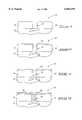
- FIG. 1is a diagrammatic sectional view of a semiconductor wafer at one processing step in accordance with the invention.
- FIG. 2is a view of the FIG. 1 wafer at a processing step subsequent to that shown by FIG. 1.
- FIG. 3is a view of the FIG. 1 wafer shown at a processing step subsequent to that shown by FIG. 2.
- FIG. 4is a view of the FIG. 1 wafer shown at a processing step subsequent to that shown by FIG. 3.
- a method of forming an electrical contact to a substrateincludes the following steps:
- a first titanium organometallic precursorto within the reactor having the substrate positioned therein, and maintaining the reactor at a temperature and a pressure which in combination are effective to deposit a first layer comprising titanium nitride onto the substrate over the node to a first thickness, the first layer of titanium nitride having incorporated carbon from the first titanium organometallic is precursor, the first layer and silicon node defining a contact interface therebetween having a first electrical resistance;
- a semiconductor wafer fragment in processis indicated generally with reference to numeral 10.
- Suchcomprises a bulk monocrystalline silicon substrate 12 having a diffusion region 14 provided therein.
- Diffusion region 14might constitute, for example, an n-type region having a conductivity dopant concentration of at least 1 ⁇ 10 19 ions/cm 3 .
- Diffusion region 14constitutes a silicon node to which electrical connection is to be made.
- An insulating layer 16is provided over substrate 12, and provided with a contact opening 18 therethrough to node 14.
- a thin layer of oxidetypically and undesirably forms atop node 14 within contact opening 18.
- Such oxideis preferably removed by plasma cleaning within a chemical vapor deposition reactor.
- Example feed gases for such plasma cleaningis include argon, H 2 , a mixture of H 2 and argon, or a reactive gas such as NF 3 .
- the substrateis biased at, for example, -100 volts to impart directionality to the ions so as to reach the bottom of contact openings and to cause greater attraction of the plasma to the substrate for such cleaning.
- a first titanium organometallic precursor and a carrier gasare injected to within the reactor, and the reactor is maintained at a temperature and pressure which in combination are effective to deposit a first layer 20 comprising titanium nitride over insulating layer 16 and node 14.
- Layer 20is provided to a first thickness which is preferably less than or equal to 100 Angstroms, and more preferably less than or equal to 50 Angstroms.
- a titanium nitride/silicon interface 25results at the base of contact opening 18.
- Interface or contact 25will have a first electrical resistance which would desirably be very low. However unfortunately, any interface between two discretely deposited or provided conductive materials will have a degree of electrical resistance thereacross. Further, and even with pre-plasma cleaning, some residual oxygen or other contaminant can remain or occur at the interface during deposition.
- Example precursors usable in accordance with the inventionare a combination of TDMAT with a carrier gas and N 2 .
- Preferred pressureis from 0.1 Torr to 10 Torr, with preferred temperature being from 200° C. to 700° C.
- a specific reduction to practice example temperature and pressurewere a wafer carrier temperature of 420° C., and a reactor pressure at 0.5 Torr.
- Titanium from the organometallic precursoris intended to combine with the nitrogen to deposit a TiN layer.
- first titanium nitride layer 20has incorporated carbon from the titanium organometallic precursor, typically in the form of titanium carbide or hydrocarbons. Such is effectively removed from the layer by an interactive plasma treatment.
- injection of the first organometallic precursoris ceased, and a first injection of a first component gas into the reactor is conducted.
- a time lagis provided between ceasing the injection of the first titanium organometallic precursor and the injection of the first component gas, with an example and preferred time lag being five seconds.
- a first plasmais generated from the first component gas against first layer 20.
- the substrateis preferably biased at a negative voltage (i.e., -100 Volts) during the reactive plasma treatment to attract ions against the substrate.
- a negative voltagei.e., -100 Volts
- An example reduction-to-practice plasma density of 10 8 to 10 9 ions/cm 3was utilized.
- High density plasmai.e., 10 11 to 10 13 ionslcm 3
- the component gashad to at least comprise hydrogen atoms and interact by chemical interaction for purposes of carbon removal.
- the first component gasdoes not necessarily comprise hydrogen atoms and does not require chemical interaction in the literal sense.
- the first component gasneed contain some component which is effective when in an activated state to interact with a component of deposited first layer 20.
- this activated state componenteffectively diffuses into the first layer and interacts with the deposited first layer component to remove carbon from the first layer and produce gaseous products which are expelled from the reactor. Carbon incorporation in the resultant film is thus minimized.
- the deposited first layer componentmight comprise unbonded and incomplete electron shell carbon atoms. The activated state component in this example would chemically react with the unbonded and incomplete electron shell atoms to drive carbon from the film.
- the component gasmight consist essentially of N 2 .
- the nitrogen plasmapresents a component (atomic or ionic nitrogen) against the deposited film.
- This componentis chemically reactive with a component of the deposited film (carbon) to remove or displace carbon from such film, and produce gaseous products (i.e., CN compounds) which are expelled from the reactor.
- the goal or intent with this exampleis to initially provide a gas which has some chemically reactive component which breaks a bond within the deposited film to cause carbon (in any of atomic, radical, or molecular radical form) to be displaced from the film and out of the reactor.
- the component from the gasmight remain in the deposited film, combine with the displaced carbon and exit the reactor, or singularly exit the reactor without combining with carbon or other material of the deposited film.
- H 2might be combined with the N 2 gas.
- atomic Nfunctions as a non-metallic bonding component to the metallic Ti, and results in conductive TiN.
- the component gasmight consist essentially of hydrogen, or a combination of two or more reactive components.
- NH 3is an example of a single component and chemically reactive gas which can present multiple components (N atoms and H atoms) which are separately reactive with components of the example TiN deposited films. Some of the N atoms would become incorporated into the film in place of the displaced carbon, while the H atoms would most likely combine with the displaced carbon to form stabilized hydrocarbons which are predominately expelled from the reactor.
- An example RF power range for plasma treatmentis from 50 to 1,000 W.
- the component gasmight consist essentially of elemental Ar.
- the interaction for carbon removal in this and the above examplesmay be chemical, physical or a combination of both.
- the plasma argon ionswould bombard the deposited film and react or impinge upon unbonded and incomplete electron shell carbon atoms to effectively drive carbon from the film. Carbon remaining deeper within the film would then outwardly diffuse to be impinged upon by more argon plasma, and be displaced from the film.
- the deposition to produce layer 20could be conducted with or without plasma enhancement, while the ion bombardment of the first plasma treatment will always involve plasma in accordance with this invention.
- the time treatment for plasma bombardmentis significantly greater (i.e., at least two times greater) than the time period for the deposition to produce layer 20.
- titanium nitride/silicon node interface 25is effectively subjected to conditions which are effective to transform interface 25 to a second electrical resistance with is lower than the first electrical resistance.
- elevated temperature exposure of interface 25can be utilized to break-up the oxide to provide Ti or TiN to extend therethrough to the node and thereby reduce contact resistance.
- interface 25might be exposed to an effective elevated temperature after the first plasma treatment to impart such lower electrical resistance.
- An example elevated temperatureis 500° C. or greater.
- the effective temperature exposurecan be utilized to effectively transform interface 25 into a titanium silicide junction 26 to the substrate, which will inherently provide a lower resistance contact. (See FIG. 3). In such event, the transformation to titanium silicide preferably consumes less than or equal to one-half of the first thickness of first layer 20 over node 14.
- a second layer 30 of titanium nitride having a preferred thickness of greater than or equal to 150 Angstromsis provided atop layer 20.
- a preferred method for providing such layeris again by repeating the injection of a second titanium organometallic precursor, preferably the same precursor, and carrier gas effective to deposit a thicker second layer 30 comprising titanium nitride. Such technique will again produce a titanium nitride layer having incorporated carbon from the second titanium organometallic precursor, typically in the form of hydrocarbon and/or titanium carbide.
- a second plasmais generated from a second component gas, preferably the same as the first component gas, within the chemical vapor deposition reactor and against second layer 30. The second plasma will effectively function the same as the first plasma to displace carbon from such layer and produce gaseous products which are expelled from the reactor.
- FIG. 4 constructionmight then be provided with a conductive plug-filling material to complete filling of contact 18, and then be polished or otherwise planarized back.
- titanium nitride layer 30might be deposited to be sufficiently thick to effectively fill and completely plug contact opening 18.
Landscapes
- Engineering & Computer Science (AREA)
- Chemical & Material Sciences (AREA)
- Physics & Mathematics (AREA)
- Computer Hardware Design (AREA)
- General Physics & Mathematics (AREA)
- Microelectronics & Electronic Packaging (AREA)
- Power Engineering (AREA)
- Manufacturing & Machinery (AREA)
- Condensed Matter Physics & Semiconductors (AREA)
- General Chemical & Material Sciences (AREA)
- Chemical Kinetics & Catalysis (AREA)
- Organic Chemistry (AREA)
- Materials Engineering (AREA)
- Mechanical Engineering (AREA)
- Metallurgy (AREA)
- Plasma & Fusion (AREA)
- Electromagnetism (AREA)
- Inorganic Chemistry (AREA)
- Internal Circuitry In Semiconductor Integrated Circuit Devices (AREA)
- Electrodes Of Semiconductors (AREA)
Abstract
Description
Ti(NR.sub.2).sub.4 +NH.sub.3 →TiN+organic by-products
Claims (35)
Priority Applications (1)
| Application Number | Priority Date | Filing Date | Title |
|---|---|---|---|
| US09/028,689US6054191A (en) | 1994-11-08 | 1998-02-24 | Method of forming an electrical contact to a silicon substrate |
Applications Claiming Priority (4)
| Application Number | Priority Date | Filing Date | Title |
|---|---|---|---|
| US08/336,260US5576071A (en) | 1994-11-08 | 1994-11-08 | Method of reducing carbon incorporation into films produced by chemical vapor deposition involving organic precursor compounds |
| US08/506,040US5661115A (en) | 1994-11-08 | 1995-07-24 | Method of reducing carbon incorporation into films produced by chemical vapor deposition involving organic precursor compounds |
| US08/587,145US5747116A (en) | 1994-11-08 | 1996-01-16 | Method of forming an electrical contact to a silicon substrate |
| US09/028,689US6054191A (en) | 1994-11-08 | 1998-02-24 | Method of forming an electrical contact to a silicon substrate |
Related Parent Applications (1)
| Application Number | Title | Priority Date | Filing Date |
|---|---|---|---|
| US08/587,145ContinuationUS5747116A (en) | 1994-11-08 | 1996-01-16 | Method of forming an electrical contact to a silicon substrate |
Publications (1)
| Publication Number | Publication Date |
|---|---|
| US6054191Atrue US6054191A (en) | 2000-04-25 |
Family
ID=46251753
Family Applications (2)
| Application Number | Title | Priority Date | Filing Date |
|---|---|---|---|
| US08/587,145Expired - LifetimeUS5747116A (en) | 1994-11-08 | 1996-01-16 | Method of forming an electrical contact to a silicon substrate |
| US09/028,689Expired - LifetimeUS6054191A (en) | 1994-11-08 | 1998-02-24 | Method of forming an electrical contact to a silicon substrate |
Family Applications Before (1)
| Application Number | Title | Priority Date | Filing Date |
|---|---|---|---|
| US08/587,145Expired - LifetimeUS5747116A (en) | 1994-11-08 | 1996-01-16 | Method of forming an electrical contact to a silicon substrate |
Country Status (1)
| Country | Link |
|---|---|
| US (2) | US5747116A (en) |
Cited By (12)
| Publication number | Priority date | Publication date | Assignee | Title |
|---|---|---|---|---|
| US6281123B1 (en)* | 1994-11-08 | 2001-08-28 | Micron Technology, Inc. | Method of reducing carbon incorporation into films produced by chemical vapor deposition involving organic precursor compounds |
| US6476432B1 (en) | 2000-03-23 | 2002-11-05 | Micron Technology, Inc. | Structures and methods for enhancing capacitors in integrated circuits |
| US20030075802A1 (en)* | 2001-07-31 | 2003-04-24 | Ammar Derraa | Boron-doped titanium nitride layer for high aspect ratio semiconductor devices |
| US20030077895A1 (en)* | 2001-08-29 | 2003-04-24 | Ammar Derraa | Diffusion barrier layer for semiconductor wafer fabrication |
| US6555471B2 (en)* | 1997-02-18 | 2003-04-29 | Micron Technology, Inc. | Method of making a void-free aluminum film |
| US20030199152A1 (en)* | 2001-08-29 | 2003-10-23 | Micron Technology, Inc. | Method of forming a conductive contact |
| US20040124532A1 (en)* | 1998-06-01 | 2004-07-01 | Matsushita Electric Industrial Co., Ltd. | Semiconductor device and method and apparatus for fabricating the same |
| US20090061623A1 (en)* | 2007-09-05 | 2009-03-05 | United Microelectronics Corp. | Method of forming electrical connection structure |
| US20100285237A1 (en)* | 2001-09-10 | 2010-11-11 | Tegal Corporation | Nanolayer deposition using bias power treatment |
| US20110030776A1 (en)* | 2009-08-10 | 2011-02-10 | Benyamin Buller | Photovoltaic device back contact |
| US20120258257A1 (en)* | 2003-02-04 | 2012-10-11 | Asm International N.V. | Nanolayer deposition process |
| US9121098B2 (en) | 2003-02-04 | 2015-09-01 | Asm International N.V. | NanoLayer Deposition process for composite films |
Families Citing this family (25)
| Publication number | Priority date | Publication date | Assignee | Title |
|---|---|---|---|---|
| US6251758B1 (en)* | 1994-11-14 | 2001-06-26 | Applied Materials, Inc. | Construction of a film on a semiconductor wafer |
| KR0164149B1 (en)* | 1995-03-28 | 1999-02-01 | 김주용 | Modification of Titanium Carbo nitride Layer |
| US5956613A (en)* | 1995-12-27 | 1999-09-21 | Lsi Logic Corporation | Method for improvement of TiN CVD film quality |
| US5895267A (en)* | 1997-07-09 | 1999-04-20 | Lsi Logic Corporation | Method to obtain a low resistivity and conformity chemical vapor deposition titanium film |
| US5976976A (en) | 1997-08-21 | 1999-11-02 | Micron Technology, Inc. | Method of forming titanium silicide and titanium by chemical vapor deposition |
| US6572933B1 (en)* | 1997-09-24 | 2003-06-03 | The Regents Of The University Of California | Forming adherent coatings using plasma processing |
| US6037252A (en)* | 1997-11-05 | 2000-03-14 | Tokyo Electron Limited | Method of titanium nitride contact plug formation |
| US6284316B1 (en)* | 1998-02-25 | 2001-09-04 | Micron Technology, Inc. | Chemical vapor deposition of titanium |
| US6143362A (en)* | 1998-02-25 | 2000-11-07 | Micron Technology, Inc. | Chemical vapor deposition of titanium |
| US6387748B1 (en)* | 1999-02-16 | 2002-05-14 | Micron Technology, Inc. | Semiconductor circuit constructions, capacitor constructions, and methods of forming semiconductor circuit constructions and capacitor constructions |
| US6291363B1 (en) | 1999-03-01 | 2001-09-18 | Micron Technology, Inc. | Surface treatment of DARC films to reduce defects in subsequent cap layers |
| US6444556B2 (en)* | 1999-04-22 | 2002-09-03 | Micron Technology, Inc. | Chemistry for chemical vapor deposition of titanium containing films |
| US6368988B1 (en) | 1999-07-16 | 2002-04-09 | Micron Technology, Inc. | Combined gate cap or digit line and spacer deposition using HDP |
| US20030015496A1 (en)* | 1999-07-22 | 2003-01-23 | Sujit Sharan | Plasma etching process |
| US6335282B1 (en)* | 1999-08-26 | 2002-01-01 | Micron Technology, Inc. | Method of forming a titanium comprising layer and method of forming a conductive silicide contact |
| US6656831B1 (en)* | 2000-01-26 | 2003-12-02 | Applied Materials, Inc. | Plasma-enhanced chemical vapor deposition of a metal nitride layer |
| US6285038B1 (en) | 2000-03-01 | 2001-09-04 | Micron Technology, Inc. | Integrated circuitry and DRAM integrated circuitry |
| EP1322951A2 (en)* | 2000-09-20 | 2003-07-02 | Molecular Reflections | Microfabricated ultrasound array for use as resonant sensors |
| US20040036129A1 (en)* | 2002-08-22 | 2004-02-26 | Micron Technology, Inc. | Atomic layer deposition of CMOS gates with variable work functions |
| KR100603703B1 (en)* | 2004-12-09 | 2006-07-20 | 매그나칩 반도체 유한회사 | Photoresist removal method and metal wiring formation method of semiconductor device using same |
| US7473637B2 (en)* | 2005-07-20 | 2009-01-06 | Micron Technology, Inc. | ALD formed titanium nitride films |
| US7709402B2 (en) | 2006-02-16 | 2010-05-04 | Micron Technology, Inc. | Conductive layers for hafnium silicon oxynitride films |
| US8039391B1 (en)* | 2006-03-27 | 2011-10-18 | Spansion Llc | Method of forming a contact in a semiconductor device with engineered plasma treatment profile of barrier metal layer |
| JP6507860B2 (en)* | 2015-06-01 | 2019-05-08 | 富士電機株式会社 | Semiconductor device manufacturing method |
| CN105590940B (en)* | 2016-02-26 | 2019-05-03 | 上海华力微电子有限公司 | Method for reducing contact resistance of metal-free silicide region of CMOS image sensor |
Citations (15)
| Publication number | Priority date | Publication date | Assignee | Title |
|---|---|---|---|---|
| US4558509A (en)* | 1984-06-29 | 1985-12-17 | International Business Machines Corporation | Method for fabricating a gallium arsenide semiconductor device |
| US4568565A (en)* | 1984-05-14 | 1986-02-04 | Allied Corporation | Light induced chemical vapor deposition of conductive titanium silicide films |
| JPH0219468A (en)* | 1988-07-05 | 1990-01-23 | Nec Corp | Formation of metal oxide |
| US4926237A (en)* | 1988-04-04 | 1990-05-15 | Motorola, Inc. | Device metallization, device and method |
| US5130172A (en)* | 1988-10-21 | 1992-07-14 | The Regents Of The University Of California | Low temperature organometallic deposition of metals |
| US5139825A (en)* | 1989-11-30 | 1992-08-18 | President And Fellows Of Harvard College | Process for chemical vapor deposition of transition metal nitrides |
| US5232871A (en)* | 1990-12-27 | 1993-08-03 | Intel Corporation | Method for forming a titanium nitride barrier layer |
| JPH05234953A (en)* | 1992-02-24 | 1993-09-10 | Matsushita Electron Corp | System and method for etching conductive thin film |
| US5300321A (en)* | 1992-05-12 | 1994-04-05 | Kawasaki Steel Corporation | Process for depositing titanium nitride film by CVD |
| US5320878A (en)* | 1992-01-10 | 1994-06-14 | Martin Marietta Energy Systems, Inc. | Method of chemical vapor deposition of boron nitride using polymeric cyanoborane |
| US5399379A (en)* | 1993-04-14 | 1995-03-21 | Micron Semiconductor, Inc. | Low-pressure chemical vapor deposition process for depositing high-density, highly-conformal titanium nitride films of low bulk resistivity |
| US5403620A (en)* | 1992-10-13 | 1995-04-04 | Regents Of The University Of California | Catalysis in organometallic CVD of thin metal films |
| US5567483A (en)* | 1995-06-05 | 1996-10-22 | Sony Corporation | Process for plasma enhanced anneal of titanium nitride |
| US5576071A (en)* | 1994-11-08 | 1996-11-19 | Micron Technology, Inc. | Method of reducing carbon incorporation into films produced by chemical vapor deposition involving organic precursor compounds |
| US5607722A (en)* | 1996-02-09 | 1997-03-04 | Micron Technology, Inc. | Process for titanium nitride deposition using five-and six-coordinate titanium complexes |
Family Cites Families (1)
| Publication number | Priority date | Publication date | Assignee | Title |
|---|---|---|---|---|
| JPH04143185A (en)* | 1990-10-03 | 1992-05-18 | Maeda Kogyo Kk | Brake lever device for bicycle |
- 1996
- 1996-01-16USUS08/587,145patent/US5747116A/ennot_activeExpired - Lifetime
- 1998
- 1998-02-24USUS09/028,689patent/US6054191A/ennot_activeExpired - Lifetime
Patent Citations (15)
| Publication number | Priority date | Publication date | Assignee | Title |
|---|---|---|---|---|
| US4568565A (en)* | 1984-05-14 | 1986-02-04 | Allied Corporation | Light induced chemical vapor deposition of conductive titanium silicide films |
| US4558509A (en)* | 1984-06-29 | 1985-12-17 | International Business Machines Corporation | Method for fabricating a gallium arsenide semiconductor device |
| US4926237A (en)* | 1988-04-04 | 1990-05-15 | Motorola, Inc. | Device metallization, device and method |
| JPH0219468A (en)* | 1988-07-05 | 1990-01-23 | Nec Corp | Formation of metal oxide |
| US5130172A (en)* | 1988-10-21 | 1992-07-14 | The Regents Of The University Of California | Low temperature organometallic deposition of metals |
| US5139825A (en)* | 1989-11-30 | 1992-08-18 | President And Fellows Of Harvard College | Process for chemical vapor deposition of transition metal nitrides |
| US5232871A (en)* | 1990-12-27 | 1993-08-03 | Intel Corporation | Method for forming a titanium nitride barrier layer |
| US5320878A (en)* | 1992-01-10 | 1994-06-14 | Martin Marietta Energy Systems, Inc. | Method of chemical vapor deposition of boron nitride using polymeric cyanoborane |
| JPH05234953A (en)* | 1992-02-24 | 1993-09-10 | Matsushita Electron Corp | System and method for etching conductive thin film |
| US5300321A (en)* | 1992-05-12 | 1994-04-05 | Kawasaki Steel Corporation | Process for depositing titanium nitride film by CVD |
| US5403620A (en)* | 1992-10-13 | 1995-04-04 | Regents Of The University Of California | Catalysis in organometallic CVD of thin metal films |
| US5399379A (en)* | 1993-04-14 | 1995-03-21 | Micron Semiconductor, Inc. | Low-pressure chemical vapor deposition process for depositing high-density, highly-conformal titanium nitride films of low bulk resistivity |
| US5576071A (en)* | 1994-11-08 | 1996-11-19 | Micron Technology, Inc. | Method of reducing carbon incorporation into films produced by chemical vapor deposition involving organic precursor compounds |
| US5567483A (en)* | 1995-06-05 | 1996-10-22 | Sony Corporation | Process for plasma enhanced anneal of titanium nitride |
| US5607722A (en)* | 1996-02-09 | 1997-03-04 | Micron Technology, Inc. | Process for titanium nitride deposition using five-and six-coordinate titanium complexes |
Non-Patent Citations (9)
| Title |
|---|
| Conrad, J.R., et al, "Ion Beam Assisted Coating And Surface Modification With Plasma Source Ion Implantation", J.Vac. Sci. Technol. A8 (4), Jul.-Aug. 1990, pp. 3146-3151. |
| Conrad, J.R., et al, Ion Beam Assisted Coating And Surface Modification With Plasma Source Ion Implantation , J.Vac. Sci. Technol. A8 (4), Jul. Aug. 1990, pp. 3146 3151.* |
| H. Watanabe, et al, "Stacked Capacitor Cells for High Density Dynamic RAM's", IED 1988, pp. 600-603, No month data. |
| H. Watanabe, et al, Stacked Capacitor Cells for High Density Dynamic RAM s , IED 1988, pp. 600 603, No month data.* |
| Intemann, et al., "Film Properties of CVD Titanium Nitride Deposited With Organometallic Precursors at Low Pressure Using Inert Gases, Ammonia, or Remote Activation," Journal of the Electrochemical Society, vol. 140, No. 11, pp. 3215-3222, No year and month data. |
| Intemann, et al., Film Properties of CVD Titanium Nitride Deposited With Organometallic Precursors at Low Pressure Using Inert Gases, Ammonia, or Remote Activation, Journal of the Electrochemical Society, vol. 140, No. 11, pp. 3215 3222, No year and month data.* |
| Miemer, Burkhard et al., Organometallic Chemical Vapor Deposition of Tungsten Metal, And Suppression Of Carbon Incorporation by Codeposition Of Platinum University of California, Department of Chemical Engineering, Aug. 4, 1992, No page data.* |
| Weber, et al., "Deposition of TiN using tetrakis(dimethylamido)-titanium in an electron-cyclotron-resonance plasma process," Applied Physics Letters, vol. 63 (3), pp. 325-327, No year and month data. |
| Weber, et al., Deposition of TiN using tetrakis(dimethylamido) titanium in an electron cyclotron resonance plasma process, Applied Physics Letters, vol. 63 (3), pp. 325 327, No year and month data.* |
Cited By (28)
| Publication number | Priority date | Publication date | Assignee | Title |
|---|---|---|---|---|
| US6495457B2 (en) | 1994-11-08 | 2002-12-17 | Micron Technology, Inc. | Method of reducing carbon incorporation into films produced by chemical vapor deposition involving organic precursor compounds |
| US6281123B1 (en)* | 1994-11-08 | 2001-08-28 | Micron Technology, Inc. | Method of reducing carbon incorporation into films produced by chemical vapor deposition involving organic precursor compounds |
| US6809025B2 (en) | 1997-02-18 | 2004-10-26 | Micron Technology, Inc. | Method of making a void-free aluminum film |
| US6555471B2 (en)* | 1997-02-18 | 2003-04-29 | Micron Technology, Inc. | Method of making a void-free aluminum film |
| US20040124532A1 (en)* | 1998-06-01 | 2004-07-01 | Matsushita Electric Industrial Co., Ltd. | Semiconductor device and method and apparatus for fabricating the same |
| US6906420B2 (en)* | 1998-06-01 | 2005-06-14 | Matsushita Electric Industrial Co., Ltd. | Semiconductor device |
| US6861330B2 (en) | 2000-03-23 | 2005-03-01 | Micron Technology Inc. | Structures and methods for enhancing capacitors in integrated circuits |
| US6696716B2 (en) | 2000-03-23 | 2004-02-24 | Micron Technology, Inc. | Structures and methods for enhancing capacitors in integrated ciruits |
| US6476432B1 (en) | 2000-03-23 | 2002-11-05 | Micron Technology, Inc. | Structures and methods for enhancing capacitors in integrated circuits |
| US6822299B2 (en) | 2001-07-31 | 2004-11-23 | Micron Technology Inc. | Boron-doped titanium nitride layer for high aspect ratio semiconductor devices |
| US6696368B2 (en) | 2001-07-31 | 2004-02-24 | Micron Technology, Inc. | Titanium boronitride layer for high aspect ratio semiconductor devices |
| US20030075802A1 (en)* | 2001-07-31 | 2003-04-24 | Ammar Derraa | Boron-doped titanium nitride layer for high aspect ratio semiconductor devices |
| US7067416B2 (en) | 2001-08-29 | 2006-06-27 | Micron Technology, Inc. | Method of forming a conductive contact |
| US6791149B2 (en) | 2001-08-29 | 2004-09-14 | Micron Technology, Inc. | Diffusion barrier layer for semiconductor wafer fabrication |
| US6888252B2 (en) | 2001-08-29 | 2005-05-03 | Micron Technology, Inc. | Method of forming a conductive contact |
| US20030199152A1 (en)* | 2001-08-29 | 2003-10-23 | Micron Technology, Inc. | Method of forming a conductive contact |
| US6746952B2 (en) | 2001-08-29 | 2004-06-08 | Micron Technology, Inc. | Diffusion barrier layer for semiconductor wafer fabrication |
| US20060246714A1 (en)* | 2001-08-29 | 2006-11-02 | Micron Technology, Inc. | Method of forming a conductive contact |
| US20030077895A1 (en)* | 2001-08-29 | 2003-04-24 | Ammar Derraa | Diffusion barrier layer for semiconductor wafer fabrication |
| US20100285237A1 (en)* | 2001-09-10 | 2010-11-11 | Tegal Corporation | Nanolayer deposition using bias power treatment |
| US9708707B2 (en) | 2001-09-10 | 2017-07-18 | Asm International N.V. | Nanolayer deposition using bias power treatment |
| US9121098B2 (en) | 2003-02-04 | 2015-09-01 | Asm International N.V. | NanoLayer Deposition process for composite films |
| US9447496B2 (en) | 2003-02-04 | 2016-09-20 | Asm International N.V. | Nanolayer deposition process |
| US20120258257A1 (en)* | 2003-02-04 | 2012-10-11 | Asm International N.V. | Nanolayer deposition process |
| US8940374B2 (en)* | 2003-02-04 | 2015-01-27 | Asm International N.V. | Nanolayer deposition process |
| US20090061623A1 (en)* | 2007-09-05 | 2009-03-05 | United Microelectronics Corp. | Method of forming electrical connection structure |
| WO2011019608A1 (en)* | 2009-08-10 | 2011-02-17 | First Solar, Inc | Photovoltaic device back contact |
| US20110030776A1 (en)* | 2009-08-10 | 2011-02-10 | Benyamin Buller | Photovoltaic device back contact |
Also Published As
| Publication number | Publication date |
|---|---|
| US5747116A (en) | 1998-05-05 |
Similar Documents
| Publication | Publication Date | Title |
|---|---|---|
| US6054191A (en) | Method of forming an electrical contact to a silicon substrate | |
| US6177145B1 (en) | Semiconductor processing method of making electrical contact to a node | |
| US5571572A (en) | Method of depositing titanium carbonitride films on semiconductor wafers | |
| US6921728B2 (en) | Method of reducing carbon incorporation into films produced by chemical vapor deposition involving organic precursor compounds | |
| US5254499A (en) | Method of depositing high density titanium nitride films on semiconductor wafers | |
| US5416045A (en) | Method for chemical vapor depositing a titanium nitride layer on a semiconductor wafer and method of annealing tin films | |
| US5691009A (en) | Method of reducing carbon incorporation into films produced by chemical vapor deposition involving organic precursor compounds | |
| US7955972B2 (en) | Methods for growing low-resistivity tungsten for high aspect ratio and small features | |
| US5637533A (en) | Method for fabricating a diffusion barrier metal layer in a semiconductor device | |
| US5278100A (en) | Chemical vapor deposition technique for depositing titanium silicide on semiconductor wafers | |
| US7838441B2 (en) | Deposition and densification process for titanium nitride barrier layers | |
| US7691749B2 (en) | Deposition of tungsten nitride | |
| US6255216B1 (en) | Methods of forming a contact having titanium silicide and titanium formed by chemical vapor deposition | |
| US7851360B2 (en) | Organometallic precursors for seed/barrier processes and methods thereof | |
| JP5490829B2 (en) | Diffusion barrier layer and method for producing the same | |
| JP2002515649A (en) | Conformal layer multi-step formation method | |
| JPH09237838A (en) | Metal wiring structure and its formation | |
| JP2760490B2 (en) | Method for manufacturing metal wiring of semiconductor element | |
| EP0867941A2 (en) | An interconnect structure for use in an intergrated circuit | |
| US20040082167A1 (en) | Methods of forming aluminum structures in microelectronic articles and articles fabricated thereby | |
| US20050250321A1 (en) | Method for fabricating semiconductor device having diffusion barrier layer | |
| US6080667A (en) | Method of treating CVD titanium nitride with silicon ions | |
| US6156656A (en) | Process for manufacturing a semiconductor device |
Legal Events
| Date | Code | Title | Description |
|---|---|---|---|
| STCF | Information on status: patent grant | Free format text:PATENTED CASE | |
| FEPP | Fee payment procedure | Free format text:PAYOR NUMBER ASSIGNED (ORIGINAL EVENT CODE: ASPN); ENTITY STATUS OF PATENT OWNER: LARGE ENTITY | |
| CC | Certificate of correction | ||
| FPAY | Fee payment | Year of fee payment:4 | |
| FPAY | Fee payment | Year of fee payment:8 | |
| FPAY | Fee payment | Year of fee payment:12 | |
| AS | Assignment | Owner name:U.S. BANK NATIONAL ASSOCIATION, AS COLLATERAL AGENT, CALIFORNIA Free format text:SECURITY INTEREST;ASSIGNOR:MICRON TECHNOLOGY, INC.;REEL/FRAME:038669/0001 Effective date:20160426 Owner name:U.S. BANK NATIONAL ASSOCIATION, AS COLLATERAL AGEN Free format text:SECURITY INTEREST;ASSIGNOR:MICRON TECHNOLOGY, INC.;REEL/FRAME:038669/0001 Effective date:20160426 | |
| AS | Assignment | Owner name:MORGAN STANLEY SENIOR FUNDING, INC., AS COLLATERAL AGENT, MARYLAND Free format text:PATENT SECURITY AGREEMENT;ASSIGNOR:MICRON TECHNOLOGY, INC.;REEL/FRAME:038954/0001 Effective date:20160426 Owner name:MORGAN STANLEY SENIOR FUNDING, INC., AS COLLATERAL Free format text:PATENT SECURITY AGREEMENT;ASSIGNOR:MICRON TECHNOLOGY, INC.;REEL/FRAME:038954/0001 Effective date:20160426 | |
| AS | Assignment | Owner name:U.S. BANK NATIONAL ASSOCIATION, AS COLLATERAL AGENT, CALIFORNIA Free format text:CORRECTIVE ASSIGNMENT TO CORRECT THE REPLACE ERRONEOUSLY FILED PATENT #7358718 WITH THE CORRECT PATENT #7358178 PREVIOUSLY RECORDED ON REEL 038669 FRAME 0001. ASSIGNOR(S) HEREBY CONFIRMS THE SECURITY INTEREST;ASSIGNOR:MICRON TECHNOLOGY, INC.;REEL/FRAME:043079/0001 Effective date:20160426 Owner name:U.S. BANK NATIONAL ASSOCIATION, AS COLLATERAL AGEN Free format text:CORRECTIVE ASSIGNMENT TO CORRECT THE REPLACE ERRONEOUSLY FILED PATENT #7358718 WITH THE CORRECT PATENT #7358178 PREVIOUSLY RECORDED ON REEL 038669 FRAME 0001. ASSIGNOR(S) HEREBY CONFIRMS THE SECURITY INTEREST;ASSIGNOR:MICRON TECHNOLOGY, INC.;REEL/FRAME:043079/0001 Effective date:20160426 | |
| AS | Assignment | Owner name:MICRON TECHNOLOGY, INC., IDAHO Free format text:RELEASE BY SECURED PARTY;ASSIGNOR:U.S. BANK NATIONAL ASSOCIATION, AS COLLATERAL AGENT;REEL/FRAME:047243/0001 Effective date:20180629 | |
| AS | Assignment | Owner name:MICRON TECHNOLOGY, INC., IDAHO Free format text:RELEASE BY SECURED PARTY;ASSIGNOR:MORGAN STANLEY SENIOR FUNDING, INC., AS COLLATERAL AGENT;REEL/FRAME:050937/0001 Effective date:20190731 |