US6052062A - Cards, communication devices, and methods of forming and encoding visibly perceptible information on the same - Google Patents
Cards, communication devices, and methods of forming and encoding visibly perceptible information on the sameDownload PDFInfo
- Publication number
- US6052062A US6052062AUS08/920,329US92032997AUS6052062AUS 6052062 AUS6052062 AUS 6052062AUS 92032997 AUS92032997 AUS 92032997AUS 6052062 AUS6052062 AUS 6052062A
- Authority
- US
- United States
- Prior art keywords
- card
- communication device
- forming
- encoding
- substrate
- Prior art date
- Legal status (The legal status is an assumption and is not a legal conclusion. Google has not performed a legal analysis and makes no representation as to the accuracy of the status listed.)
- Expired - Lifetime
Links
Images


Classifications
- G—PHYSICS
- G06—COMPUTING OR CALCULATING; COUNTING
- G06K—GRAPHICAL DATA READING; PRESENTATION OF DATA; RECORD CARRIERS; HANDLING RECORD CARRIERS
- G06K19/00—Record carriers for use with machines and with at least a part designed to carry digital markings
- G06K19/06—Record carriers for use with machines and with at least a part designed to carry digital markings characterised by the kind of the digital marking, e.g. shape, nature, code
- G06K19/06009—Record carriers for use with machines and with at least a part designed to carry digital markings characterised by the kind of the digital marking, e.g. shape, nature, code with optically detectable marking
- G06K19/06046—Constructional details
- G—PHYSICS
- G06—COMPUTING OR CALCULATING; COUNTING
- G06K—GRAPHICAL DATA READING; PRESENTATION OF DATA; RECORD CARRIERS; HANDLING RECORD CARRIERS
- G06K19/00—Record carriers for use with machines and with at least a part designed to carry digital markings
- G06K19/06—Record carriers for use with machines and with at least a part designed to carry digital markings characterised by the kind of the digital marking, e.g. shape, nature, code
- G06K19/067—Record carriers with conductive marks, printed circuits or semiconductor circuit elements, e.g. credit or identity cards also with resonating or responding marks without active components
- G06K19/07—Record carriers with conductive marks, printed circuits or semiconductor circuit elements, e.g. credit or identity cards also with resonating or responding marks without active components with integrated circuit chips
- G06K19/077—Constructional details, e.g. mounting of circuits in the carrier
Definitions
- the present inventionrelates to cards, communication devices, and methods of forming and encoding visibly perceptible information on the same.
- Radio frequency identification device (RFID) cardstypically include printed information regarding the manufacture or issuance of the card on a face of the card.
- the faces of such cardsare normally used for advertising, embossing, and providing signature panels, magnetic stripes, or end user information. Alternatively, such information regarding the manufacture or issuance of the card is not provided at all.
- One embodiment of the present inventionprovides a remote intelligent communication device (RIC).
- the embodimentincludes a card-thin housing including at least one side having visibly perceptible information thereon and communication circuitry within the housing and configured to at least one of communicate (i.e., output) and receive electronic signals.
- Other embodiments of the present inventionprovide additional electronic communication devices including a radio frequency identification device.
- the remote intelligent communication device and radio frequency identification devicesare wireless communication devices according to preferred embodiments of the present invention.
- a second aspect of the present inventionprovides a card having plural surfaces, and a side intermediate the surfaces.
- the sidehas a thickness less than about 100 mils. Indicia is provided on the side.
- a communication deviceincludes a substrate having a support surface, an antenna, transponder circuitry, and a battery.
- a cured resinis provided upon the support surface, the antenna, the transponder circuitry and the battery.
- the cured resin and substrateform a housing.
- Identification indicais encoded on at least one of the side surfaces of the housing.
- Another aspect of the present inventionprovides a method of forming a card including moving at least one of a card and a print head relative to the other of the card and print head.
- the methodadditionally includes encoding visibly perceptible information on a side of the card.
- An additional aspect of the present inventionprovides a method of forming a communication device.
- This methodincludes the steps of providing a substrate, an antenna, and communication circuitry and applying and curing an encapsulant to form a housing.
- the methodfurther includes encoding visibly perceptible information on a side surface of the housing.
- Another aspectprovides a method of forming a remote intelligent communication device. Additional methods according to the present invention provide methods of encoding visibly perceptible information on a communication device.
- FIG. 1is a block diagram of an electronic communication system including an interrogator and an electronic communication device.
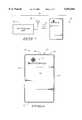
- FIG. 2is a front elevational view of the electronic communication device.
- FIG. 3is a front elevational view of the electronic communication device at an intermediate processing step.
- FIG. 4is an isometric view of the electronic communication device of FIG. 2 having indicia on a side thereof in accordance with the present invention.
- FIG. 5is an illustrative diagram of a first method and system for providing indicia upon a side of the electronic communication device.
- FIG. 6is an illustrative diagram of another method and system for providing indicia upon a side of the electronic communication device.
- the present inventionprovides indicia or other visibly perceptible information upon a side or edge of a card.
- the present inventionis described with reference to the providing of indicia upon a side of an electronic communication device provided in the form of a card.
- Such indiciamay be applied to other types of cards, including, for example, credit cards, smart cards, badges, tags, stamps and labels.
- such indiciamay be applied to any device having a card-thin housing.
- card-thinrefers to a housing or other supportive substrate having a thickness less than 200 mils, and preferably less than 100 mils.
- the electronic communication deviceis fabricated in a card configuration in the described embodiment.
- the described embodiment of the electronic communication devicediscloses a wireless communication device.
- the embodimentis illustrative and other configurations of cards, and electronic communication devices within card-thin housings are possible.
- Exemplary embodiments of electronic communication devices within such housingscomprise radio frequency identification devices (RFID) and remote intelligent communication devices (RIC).
- RFIDradio frequency identification devices
- RICremote intelligent communication devices
- Remote intelligent communication devicesare capable of functions other than the identifying function of radio frequency identification devices.
- an electronic communication device provided in a card configuration 10comprises part of a wireless communication system 12.
- the illustrated communication system 12further includes an interrogator unit 14.
- An exemplary wireless communication system 12is described in U.S. patent application Ser. No. 08/705,043, filed Aug. 29, 1996, assigned to the assignee of the present application and incorporated herein by reference.
- An exemplary interrogator 14is described in detail in U.S. patent application Ser. No. 08/806,158, filed Feb. 25, 1997, assigned to the assignee of the present application and incorporated herein by reference.
- the electronic communication device or card 10communicates via electronic signals with interrogator unit 14.
- device or card 10communicates with unit 14 via wireless electronic signals, such as radio frequency (RF) signals.
- RFradio frequency
- Wireless electronic signals or radio frequency signalswhich include microwave signals, are utilized for communications in the preferred embodiment of communication system 12.
- Communication system 12further includes an antenna 16 coupled to the interrogator unit 14 to facilitate communications.
- Electronic communication arrangements other than wirelessare possible within the present invention.
- the illustrated card 10includes an insulative first substrate or layer of supportive material 18.
- Example materials for substrate 18comprise polyester, polyethylene or polyimide film having a thickness of 4-6 mils (thousandths of an inch).
- a plurality of ink layersare applied to substrate 18 in other embodiments of the invention.
- Substrate 18includes an outer periphery 21.
- the substrate 18defines a first portion of a housing for the electronic communication device or card 10.
- a ground planecan be provided over substrate 18 to improve the wireless communications of card 10.
- a dielectric layeris ideally provided over the ground plane in such embodiments.
- An exemplary card 10includes an upper surface 40, a lower surface 42 (not shown in FIG. 2) opposite surface 40, and a plurality of side surfaces 41 intermediate upper and lower surfaces 40, 42.
- Inkscan be used to convey information such as logos and/or company names, such as those illustrated at 11. The inks may be viewed upon upper surface 40 of card 10.
- a patterned conductive trace 30is formed or applied over a support surface 25 of substrate 18.
- a preferred conductive trace 30comprises silver ink or printed thick film (PTF).
- PTFprinted thick film
- One manner of forming or applying the conductive inkis to screen print the ink on the support surface 25 of substrate 18 through conventional screen printing techniques.
- the conductive inkforms desired electrical connections with and between electronic components which will be described below.
- substrate 18forms a portion of a larger roll of polyester film material
- the printing of the conductive trace 30can take place simultaneously for a number of the to-be-formed electronic communication devices.
- the illustrated conductive trace 30provides antennas 32, 34 which are suitable for respectively receiving and transmitting electronic signals or RF energy.
- the illustrated antenna 32constitutes a loop antenna. Other antenna constructions are possible.
- antenna 34is omitted and antenna 32 is configured to both receive and transmit electronic signals.
- Substrate 18includes outer periphery 21 inside of which a portion, and preferably the entire antenna 32 extends or lies.
- the antenna 32is preferably provided within the confines of periphery 21.
- antenna 32has a length within the range of 80 mm-95 mm and is tuned to a frequency of 2.45 GHz.
- Conductive trace 30additionally includes a plurality of power source terminals, including a first connection terminal 53 (shown in phantom in FIG. 3) and a second connection terminal 58. Connection terminals 53, 58 are formed on support surface 25 of card 10.
- the illustrated card 10includes a power source 52 and integrated circuit 54 individually mounted on support surface 25 and supported by substrate 18.
- Power source 52is provided within antenna 32 in the depicted embodiment.
- Passive componentse.g., capacitors 57 may also be mounted on support surface 25.
- Power source 52provides operational power to electrical components within card 10, including integrated circuit 54.
- power source 52is a battery.
- the batteryis preferably a thin profile battery which includes first and second terminals of opposite polarity. More particularly, the battery has a lid or negative (i.e., ground) terminal or electrode, and a can or positive (i.e., power) terminal or electrode.
- Conductive epoxyis applied over desired areas of the support surface 25 using conventional printing techniques, such as stencil printing, to assist in component attachment described just below. Alternately, solder or another conductive material is employed instead of conductive epoxy.
- Power source 52 and integrated circuit 54are provided and conductively bonded on the support surface 25 using the conductive epoxy.
- Integrated circuit 54can be mounted either before or after the power source 52 is mounted on the support surface 25.
- First and second connection terminals 53, 58are coupled to the integrated circuit 54 by conductive epoxy in accordance with a preferred embodiment of the invention.
- the conductive epoxyalso electrically connects the first terminal of the power source 52 to the first connection terminal 53.
- power source 52is placed lid down such that the conductive epoxy makes electrical contact between the negative terminal of the power source 52 and the first connection terminal 53.
- Power source 52has a perimetral edge 56, defining the second power source terminal, which is disposed adjacent second connection terminal 58.
- perimetral edge 56 of the power source 52is cylindrical
- the connection terminal 58is arcuate and has a radius slightly greater than the radius of the power source 52, so that connection terminal 58 is closely spaced apart from the edge 56 of power source 52.
- perimetral edge 56defines the can of the power source 52, such that the conductive epoxy connects the positive terminal of the power source 52 to connection terminal 58.
- the conductive epoxyis then cured.
- First and second connection terminals 53, 58are coupled with integrated circuit 54 providing operational power and an electrical ground reference thereto.
- Antenna 32is coupled with the integrated circuit 54 providing electrical connection therebetween for the transfer of signals corresponding to the wireless electronic signals or RF energy transmitted and received by antenna 32.
- Integrated circuit 54includes suitable communication circuitry for providing wireless communications capabilities within electronic communication device 10.
- integrated circuit 54includes a processor 62, memory 63, and transponder circuitry 64 for providing wireless communications with interrogator unit 14.
- An exemplary and preferred integrated circuitry package 54is described in U.S. patent application Ser. No. 08/705,043 incorporated by reference above.
- One embodiment of the communication circuitry or transponder circuitry 64includes a modulator and a receiver operable to respectively communicate (i.e., output) and receive wireless electronic signals.
- the processor 62is coupled with transponder circuitry 64 and is configured to process the electronic signals. Responsive to the detection of an appropriate polling signal, processor 62 instructs modulator transponder circuitry 64 to output a identification signal.
- the wireless electronic signalsare transmitted and received via antenna 32 in the illustrated embodiment.
- the receiver of transponder circuitry 64is configured to receive electronic (e.g., wireless) signals and the modulator is configured to output or communicate electronic (e.g., wireless) signals.
- the modulatorcomprises an active transmitter or a backscatter device according to certain embodiments. Such outputting or communicating of the electronic signals via the modulator comprises one of transmitting the electronic signals and reflecting received signals.
- the modulatoris configured to communicate an identification signal responsive to the reception of an appropriate polling signal.
- the identification signal outputted via the modulatoridentifies the particular card 10 communicating the identification signal in accordance with one embodiment of the present invention.
- the identification signalcorresponds to identification indicia (described in detail below) encoded upon a side surface 41 of the card 10.
- an encapsulant 44such as an encapsulating epoxy resin material, is subsequently formed to encapsulate a portion of the substrate 18.
- Resin encapsulant 44covers integrated circuit 54, power source 52, conductive circuitry 30, and a portion of the support surface of substrate 18.
- Resin encapsulant 44 and substrate 18define the card-thin housing 27 of the card 10.
- Substrate 18comprises the upper surface 40 of card 10 and encapsulant 44 comprises the lower surface 42 of card 10.
- housing 27 of card 10has a length of about 3.375 inches, a width of about 2.125 inches, and a thickness less than or equal to about 0.090 inches.
- the thickness of the sides 41is less than the lengths and widths of upper surface 40 and lower surface 42 in the described embodiment.
- An exemplary resin encapsulant 44is a flowable encapsulant.
- the flowable encapsulant 44is flowed to encapsulate substrate 18.
- Encapsulant 44is subsequently cured following the appropriate covering of the integrated circuit 54, power source 52, conductive circuitry 30, and support surface of substrate 18.
- the curing of encapsulant 44forms a composite substrate or solid housing 27 which comprises substrate 18 and encapsulant 44.
- such epoxy encapsulant 44constitutes a two-part epoxy having a resin and a hardener which are sufficient to provide a desired degree of flexible rigidity. Further details regarding encapsulation of electronic communication device 10 are described in U.S. patent application Ser. No. 08/800,037, filed Feb. 13, 1997, assigned to the assignee of the present application, and incorporated herein by reference.
- FIG. 4some of the sides or side surfaces or edge surfaces 41 of card 10 are shown.
- the sides 41extend intermediate upper surface 40 and lower surface 42.
- Substrate 18 and encapsulant 44form sides 41 of the illustrated card 10.
- visibly perceptible information 43is provided upon one or more sides 41 of card 10.
- visibly perceptible information 43comprises alphanumeric characters which are provided upon the encapsulant 44.
- the illustrated visibly perceptible information 43comprises identification indicia. More specifically, the illustrated identification indicia identifies the assignee of this patent application, and the date of manufacture and a lot number corresponding to the particular card 10 upon which the indicia is encoded. In particular, identification indicia can identify the particular electronic communication device or card 10 upon which the indicia is encoded.
- Visibly perceptible information 43can additionally include information regarding issuance of the card 10 for facilitating the tracking thereof. Visibly perceptible information 43 can comprise more, less or other information.
- the height of the visibly perceptible information 43is represented by dimension "h" in FIG. 4.
- the height of visibly perceptible information 43can vary depending upon the dimensions of the specific card 10.
- a height of visibly perceptible information 43 of less than 50 milsis utilized and preferred.
- one exemplary card 10 comprising an electronic communication device having a thickness less than 90 milswas provided with visibly perceptible information 43 having a height less than 47 mils encoded on a side thereof.
- Information or indiciamay be provided upon cards of other dimensions according to other embodiments of the present invention.
- the visibly perceptible information 43is provided upon conventional cards, such as credit cards, according to the alternative embodiments. Such cards are typically only 30 mils thick (in accordance with the International Standards Organization).
- One method of encoding the visibly perceptible information 43 on the card 10includes printing.
- the present inventionencompasses additional methods of providing the visibly perceptible information on sides 41 of a card 10.
- encodingcomprises scribing or embossing the visibly perceptible information 43 onto the sides 41 of the card 10 in other embodiments.
- FIG. 5 and FIG. 6two exemplary methods of providing the visibly perceptible information 43 upon at least one of the sides 41 of the cards 10 are shown.
- the depicted methodsprovide for printing the visibly perceptible information 43 onto the sides of the cards 10.
- a printing station 72comprises a holding apparatus 61 and a print head 66 configured to print visibly perceptible information 43 upon side surface 41 of the card 10.
- Apparatus 61comprises a base support structure 67 and a holding member 69.
- the illustrated base support structure 67includes a raised edge 65 for assisting with the holding of the card 10 to be processed.
- Holding member 69is provided in an opposing relation to raised edge 65 and is configured hold a card 10 in preferably perpendicular or upright position therebetween.
- Holding member 69is configured to move toward and away from raised edge 65 to respectively hold the card 10 for printing, or permit removal of a processed card 10 or insertion of a card 10 to be processed. Holding member 69 and edge 65 operate to support the card 10 at one side thereof.
- Print head 61is operable to encode the visibly perceptible information 43 upon side surface 41 of card 10.
- Additional print headsmay be provided to simultaneously print on plural side surfaces 41 of card 10.
- the card 10 to be processedremains stationary during the printing thereon by the print head 66 shown in FIG. 5.
- the depicted holding member 69is shorter than the card 10 enabling printing on the upper side 41 thereof.
- holding member 65is approximately the same length, or slightly less than the length of card 10.
- the cards to be processedare preferably provided in a pre-arranged orientation or stack 68.
- the stack 68is provided adjacent a selection roller 73 operable to select a card 10 from stack 68 for processing.
- One card 10may be selected while the other cards remain in the prearranged stack 68.
- processing rollers 70move card 10 relative to or past stationary print head 66 during the printing of visibly perceptible information 43 on the side surface 41 thereof.
- Printing stations 72, 72ainclude an X-Y grid ink jet plotter according to one aspect of the present invention. More specifically, an exemplary print head 66 comprises a Videojet EXCEL High Resolution Model, available from Video Jet of Woodale, Ill.
- the visibly perceptible information or indicia 43is provided upon encapsulant 44.
- Numerous conventional cardse.g., credit cards
- Numerous conventional cardscomprise materials such as polyvinyl chloride (PVC) or ABS.
- PVCpolyvinyl chloride
- ABSpolyvinyl chloride
- Such materialsallow standard inks to be used for printing the visibly perceptible information 43 on sides 41 of cards 10 by ink jet printing or pad printing.
Landscapes
- Engineering & Computer Science (AREA)
- Physics & Mathematics (AREA)
- General Physics & Mathematics (AREA)
- Theoretical Computer Science (AREA)
- Computer Hardware Design (AREA)
- Microelectronics & Electronic Packaging (AREA)
- Credit Cards Or The Like (AREA)
Abstract
Description
Claims (49)
Priority Applications (2)
| Application Number | Priority Date | Filing Date | Title |
|---|---|---|---|
| US08/920,329US6052062A (en) | 1997-08-20 | 1997-08-20 | Cards, communication devices, and methods of forming and encoding visibly perceptible information on the same |
| US09/524,804US7221257B1 (en) | 1997-08-20 | 2000-03-14 | Wireless communication devices, radio frequency identification devices, methods of forming a wireless communication device, and methods of forming a radio frequency identification device |
Applications Claiming Priority (1)
| Application Number | Priority Date | Filing Date | Title |
|---|---|---|---|
| US08/920,329US6052062A (en) | 1997-08-20 | 1997-08-20 | Cards, communication devices, and methods of forming and encoding visibly perceptible information on the same |
Related Child Applications (1)
| Application Number | Title | Priority Date | Filing Date |
|---|---|---|---|
| US09/524,804ContinuationUS7221257B1 (en) | 1997-08-20 | 2000-03-14 | Wireless communication devices, radio frequency identification devices, methods of forming a wireless communication device, and methods of forming a radio frequency identification device |
Publications (1)
| Publication Number | Publication Date |
|---|---|
| US6052062Atrue US6052062A (en) | 2000-04-18 |
Family
ID=25443568
Family Applications (2)
| Application Number | Title | Priority Date | Filing Date |
|---|---|---|---|
| US08/920,329Expired - LifetimeUS6052062A (en) | 1997-08-20 | 1997-08-20 | Cards, communication devices, and methods of forming and encoding visibly perceptible information on the same |
| US09/524,804Expired - Fee RelatedUS7221257B1 (en) | 1997-08-20 | 2000-03-14 | Wireless communication devices, radio frequency identification devices, methods of forming a wireless communication device, and methods of forming a radio frequency identification device |
Family Applications After (1)
| Application Number | Title | Priority Date | Filing Date |
|---|---|---|---|
| US09/524,804Expired - Fee RelatedUS7221257B1 (en) | 1997-08-20 | 2000-03-14 | Wireless communication devices, radio frequency identification devices, methods of forming a wireless communication device, and methods of forming a radio frequency identification device |
Country Status (1)
| Country | Link |
|---|---|
| US (2) | US6052062A (en) |
Cited By (28)
| Publication number | Priority date | Publication date | Assignee | Title |
|---|---|---|---|---|
| US20010002826A1 (en)* | 1997-05-01 | 2001-06-07 | Mark E. Tuttle | Embedded circuits |
| US6326889B1 (en) | 1999-07-29 | 2001-12-04 | Micron Technology, Inc. | Radio frequency identification device and methods of determining a communication range of an interrogator of a wireless identification system |
| US6366260B1 (en)* | 1998-11-02 | 2002-04-02 | Intermec Ip Corp. | RFID tag employing hollowed monopole antenna |
| US20020130817A1 (en)* | 2001-03-16 | 2002-09-19 | Forster Ian J. | Communicating with stackable objects using an antenna array |
| US6459376B2 (en)* | 1999-07-29 | 2002-10-01 | Micron Technology, Inc. | Radio frequency identification devices, remote communication devices, wireless communication systems, and methods of indicating operation |
| US20040036657A1 (en)* | 2002-04-24 | 2004-02-26 | Forster Ian J. | Energy source communication employing slot antenna |
| US20040080299A1 (en)* | 2002-04-24 | 2004-04-29 | Forster Ian J. | Energy source recharging device and method |
| US20040106376A1 (en)* | 2002-04-24 | 2004-06-03 | Forster Ian J. | Rechargeable interrogation reader device and method |
| US20050083201A1 (en)* | 1999-07-29 | 2005-04-21 | Trosper Scott T. | Radio frequency identification devices, remote communication devices, identification systems, communication methods, and identification methods |
| WO2005079122A1 (en)* | 2004-02-11 | 2005-08-25 | Cstar Technologies Inc. | Method and apparatus for cataloguing and poling movement in an environment for purposes of tracking and/or containment of infectious diseases |
| US20060097849A1 (en)* | 1997-08-18 | 2006-05-11 | Dando Ross S | Wireless communication devices and methods of forming and operating the same |
| US20070007345A1 (en)* | 1997-08-20 | 2007-01-11 | Tuttle Mark E | Electronic communication devices, methods of forming electrical communication devices, and communications methods |
| US20070040685A1 (en)* | 1992-08-12 | 2007-02-22 | Tuttle John R | Miniature radio frequency transceiver |
| US7221257B1 (en)* | 1997-08-20 | 2007-05-22 | Micron Technology, Inc. | Wireless communication devices, radio frequency identification devices, methods of forming a wireless communication device, and methods of forming a radio frequency identification device |
| US20080111675A1 (en)* | 2006-11-10 | 2008-05-15 | Micron Technology, Inc. | Tracking systems, passive RFIDs, methods of locating and identifying RFIDs, and methods of tracking items |
| US20080186178A1 (en)* | 2007-02-07 | 2008-08-07 | Micron Technology, Inc. | RFIDS, interrogators, indication systems, methods of determining a bi-directional communication range of an interrogator, methods of activating an observable indicator, and methods of indicating bi-directional functionality of a radio connection |
| US20080291027A1 (en)* | 1998-02-12 | 2008-11-27 | Lake Rickie C | Thin Profile Battery Bonding Method, Method Of Conductively Interconnecting Electronic Components, Battery Powerable Apparatus, Radio Frequency Communication Device, And Electric Circuit |
| USRE42773E1 (en) | 1992-06-17 | 2011-10-04 | Round Rock Research, Llc | Method of manufacturing an enclosed transceiver |
| US20130251915A1 (en)* | 2009-05-19 | 2013-09-26 | Apple Inc. | Techniques for marking product housings |
| US20130255078A1 (en)* | 2012-04-03 | 2013-10-03 | X-Card Holdings, Llc | Information carrying card comprising a cross-linked polymer composition, and method of making the same |
| ES2430405A1 (en)* | 2013-08-06 | 2013-11-20 | Smart Layer 3, S.L. | Method for decorating the sides of plastic cards |
| US20150116095A1 (en)* | 2013-09-30 | 2015-04-30 | Bibliotheca Limited | Reader, writer and method for programmable tags |
| US9439334B2 (en) | 2012-04-03 | 2016-09-06 | X-Card Holdings, Llc | Information carrying card comprising crosslinked polymer composition, and method of making the same |
| US20170148743A1 (en)* | 2015-11-25 | 2017-05-25 | Infineon Technologies Austria Ag | Semiconductor chip package comprising side wall marking |
| US10028120B2 (en)* | 2015-02-18 | 2018-07-17 | Global Life-Line, Inc. | Identification card holder with personal locator |
| US10906287B2 (en) | 2013-03-15 | 2021-02-02 | X-Card Holdings, Llc | Methods of making a core layer for an information carrying card, and resulting products |
| US11361204B2 (en) | 2018-03-07 | 2022-06-14 | X-Card Holdings, Llc | Metal card |
| US12220897B2 (en) | 2022-10-20 | 2025-02-11 | X-Card Holdings, Llc | Core layer for information carrying card, resulting information carrying card, and methods of making the same |
Families Citing this family (5)
| Publication number | Priority date | Publication date | Assignee | Title |
|---|---|---|---|---|
| US7405656B2 (en)* | 2004-01-30 | 2008-07-29 | United Parcel Service Of America, Inc. | Device and method for encapsulation and mounting of RFID devices |
| US20070093200A1 (en)* | 2005-10-21 | 2007-04-26 | Delphi Technologies, Inc. | Communications device for communicating between a vehicle and a call center |
| USD602015S1 (en)* | 2008-04-07 | 2009-10-13 | Apple Inc. | Electronic device |
| US9652909B1 (en)* | 2015-11-06 | 2017-05-16 | Amazon Technologies, Inc. | Security badge |
| USD823395S1 (en) | 2015-11-06 | 2018-07-17 | Amazon Technologies, Inc. | Identification badge |
Citations (10)
| Publication number | Priority date | Publication date | Assignee | Title |
|---|---|---|---|---|
| US4075632A (en)* | 1974-08-27 | 1978-02-21 | The United States Of America As Represented By The United States Department Of Energy | Interrogation, and detection system |
| US4461793A (en)* | 1983-02-07 | 1984-07-24 | W. H. Brady Co. | Printable coating for heatshrinkable materials |
| US4593185A (en)* | 1983-02-18 | 1986-06-03 | Zeiss Ikon Ag | Safety lock |
| US4926182A (en)* | 1986-05-30 | 1990-05-15 | Sharp Kabushiki Kaisha | Microwave data transmission apparatus |
| US5166680A (en)* | 1989-06-16 | 1992-11-24 | Ganis - Smart Park Systems Ltd. | Portable parking meter device and method of operating same |
| US5245329A (en)* | 1989-02-27 | 1993-09-14 | Security People Inc. | Access control system with mechanical keys which store data |
| US5462374A (en)* | 1992-02-25 | 1995-10-31 | Sony Corporation | Card printing apparatus |
| US5493437A (en)* | 1993-09-13 | 1996-02-20 | Motorola | External communication link for a credit card pager |
| US5621412A (en)* | 1994-04-26 | 1997-04-15 | Texas Instruments Incorporated | Multi-stage transponder wake-up, method and structure |
| US5649296A (en)* | 1995-06-19 | 1997-07-15 | Lucent Technologies Inc. | Full duplex modulated backscatter system |
Family Cites Families (7)
| Publication number | Priority date | Publication date | Assignee | Title |
|---|---|---|---|---|
| US4782342A (en)* | 1986-08-04 | 1988-11-01 | Walton Charles A | Proximity identification system with lateral flux paths |
| US5192947A (en)* | 1990-02-02 | 1993-03-09 | Simon Neustein | Credit card pager apparatus |
| JP2736023B2 (en)* | 1994-12-27 | 1998-04-02 | ユニデン株式会社 | Vibrator mounting structure, vibrator mounting holder, and vibrator mounting method |
| US5598169A (en)* | 1995-03-24 | 1997-01-28 | Lucent Technologies Inc. | Detector and modulator circuits for passive microwave links |
| US6104333A (en)* | 1996-12-19 | 2000-08-15 | Micron Technology, Inc. | Methods of processing wireless communication, methods of processing radio frequency communication, and related systems |
| US6052062A (en)* | 1997-08-20 | 2000-04-18 | Micron Technology, Inc. | Cards, communication devices, and methods of forming and encoding visibly perceptible information on the same |
| US6100804A (en)* | 1998-10-29 | 2000-08-08 | Intecmec Ip Corp. | Radio frequency identification system |
- 1997
- 1997-08-20USUS08/920,329patent/US6052062A/ennot_activeExpired - Lifetime
- 2000
- 2000-03-14USUS09/524,804patent/US7221257B1/ennot_activeExpired - Fee Related
Patent Citations (10)
| Publication number | Priority date | Publication date | Assignee | Title |
|---|---|---|---|---|
| US4075632A (en)* | 1974-08-27 | 1978-02-21 | The United States Of America As Represented By The United States Department Of Energy | Interrogation, and detection system |
| US4461793A (en)* | 1983-02-07 | 1984-07-24 | W. H. Brady Co. | Printable coating for heatshrinkable materials |
| US4593185A (en)* | 1983-02-18 | 1986-06-03 | Zeiss Ikon Ag | Safety lock |
| US4926182A (en)* | 1986-05-30 | 1990-05-15 | Sharp Kabushiki Kaisha | Microwave data transmission apparatus |
| US5245329A (en)* | 1989-02-27 | 1993-09-14 | Security People Inc. | Access control system with mechanical keys which store data |
| US5166680A (en)* | 1989-06-16 | 1992-11-24 | Ganis - Smart Park Systems Ltd. | Portable parking meter device and method of operating same |
| US5462374A (en)* | 1992-02-25 | 1995-10-31 | Sony Corporation | Card printing apparatus |
| US5493437A (en)* | 1993-09-13 | 1996-02-20 | Motorola | External communication link for a credit card pager |
| US5621412A (en)* | 1994-04-26 | 1997-04-15 | Texas Instruments Incorporated | Multi-stage transponder wake-up, method and structure |
| US5649296A (en)* | 1995-06-19 | 1997-07-15 | Lucent Technologies Inc. | Full duplex modulated backscatter system |
Cited By (79)
| Publication number | Priority date | Publication date | Assignee | Title |
|---|---|---|---|---|
| USRE42773E1 (en) | 1992-06-17 | 2011-10-04 | Round Rock Research, Llc | Method of manufacturing an enclosed transceiver |
| US8018340B2 (en) | 1992-08-12 | 2011-09-13 | Round Rock Research, Llc | System and method to track articles at a point of origin and at a point of destination using RFID |
| US20070290812A1 (en)* | 1992-08-12 | 2007-12-20 | Tuttle John R | Miniature Radio Frequency Transceiver |
| US20070040685A1 (en)* | 1992-08-12 | 2007-02-22 | Tuttle John R | Miniature radio frequency transceiver |
| US20010002826A1 (en)* | 1997-05-01 | 2001-06-07 | Mark E. Tuttle | Embedded circuits |
| US20060097849A1 (en)* | 1997-08-18 | 2006-05-11 | Dando Ross S | Wireless communication devices and methods of forming and operating the same |
| US7948382B2 (en)* | 1997-08-20 | 2011-05-24 | Round Rock Research, Llc | Electronic communication devices, methods of forming electrical communication devices, and communications methods |
| US7839285B2 (en) | 1997-08-20 | 2010-11-23 | Round Rock Resarch, LLC | Electronic communication devices, methods of forming electrical communication devices, and communications methods |
| US7221257B1 (en)* | 1997-08-20 | 2007-05-22 | Micron Technology, Inc. | Wireless communication devices, radio frequency identification devices, methods of forming a wireless communication device, and methods of forming a radio frequency identification device |
| US20070007345A1 (en)* | 1997-08-20 | 2007-01-11 | Tuttle Mark E | Electronic communication devices, methods of forming electrical communication devices, and communications methods |
| US20080291027A1 (en)* | 1998-02-12 | 2008-11-27 | Lake Rickie C | Thin Profile Battery Bonding Method, Method Of Conductively Interconnecting Electronic Components, Battery Powerable Apparatus, Radio Frequency Communication Device, And Electric Circuit |
| US6366260B1 (en)* | 1998-11-02 | 2002-04-02 | Intermec Ip Corp. | RFID tag employing hollowed monopole antenna |
| US20070035395A1 (en)* | 1999-07-29 | 2007-02-15 | Trosper Scott T | Wireless communication devices, radio frequency identification devices, radio frequency identification device communication systems, wireless communication methods, and radio frequency identification device communication methods |
| US6545605B2 (en) | 1999-07-29 | 2003-04-08 | Micron Technology, Inc. | Methods of determining a communications range of an interrogator of a wireless identification system and methods of verifying operation of a wireless identification system |
| US7071824B2 (en) | 1999-07-29 | 2006-07-04 | Micron Technology, Inc. | Radio frequency identification devices, remote communication devices, identification systems, communication methods, and identification methods |
| US8004407B2 (en) | 1999-07-29 | 2011-08-23 | Round Rock Research, Llc | Radio frequency identification devices, remote communication devices, identification systems, communication methods, and identification methods |
| US7123148B2 (en) | 1999-07-29 | 2006-10-17 | Micron Technology, Inc. | Wireless communication devices, radio frequency identification devices, radio frequency identification device communication systems, wireless communication methods, and radio frequency identification device communication methods |
| US6452496B1 (en) | 1999-07-29 | 2002-09-17 | Micron Technology, Inc. | Radio frequency identification devices and a method of determining a communication range |
| US6326889B1 (en) | 1999-07-29 | 2001-12-04 | Micron Technology, Inc. | Radio frequency identification device and methods of determining a communication range of an interrogator of a wireless identification system |
| US20050083201A1 (en)* | 1999-07-29 | 2005-04-21 | Trosper Scott T. | Radio frequency identification devices, remote communication devices, identification systems, communication methods, and identification methods |
| US8253565B2 (en) | 1999-07-29 | 2012-08-28 | Round Rock Research, Llc | Radio frequency identification devices, remote communication devices, identification systems, communication methods, and identification methods |
| US6459376B2 (en)* | 1999-07-29 | 2002-10-01 | Micron Technology, Inc. | Radio frequency identification devices, remote communication devices, wireless communication systems, and methods of indicating operation |
| US7737851B2 (en) | 1999-07-29 | 2010-06-15 | Round Rock Research, Llc | Radio frequency identification devices, remote communication devices, identification systems, communication methods, and identification methods |
| US20100013637A1 (en)* | 1999-07-29 | 2010-01-21 | Keystone Technology Solutions, Llc | Radio Frequency Identification Devices, Remote Communication Devices, Identification Systems, Communication Methods, and Identification Methods |
| US6466130B2 (en) | 1999-07-29 | 2002-10-15 | Micron Technology, Inc. | Wireless communication devices, wireless communication systems, communication methods, methods of forming radio frequency identification devices, methods of testing wireless communication operations, radio frequency identification devices, and methods of forming radio frequency identification devices |
| US7518515B2 (en) | 1999-07-29 | 2009-04-14 | Keystone Technology Solutions, Llc | Method and system for RFID communication |
| US8487766B2 (en) | 1999-07-29 | 2013-07-16 | Round Rock Research, LLP | Radio frequency identification devices, remote communication devices, identification systems, communication methods, and identification methods |
| US20020130817A1 (en)* | 2001-03-16 | 2002-09-19 | Forster Ian J. | Communicating with stackable objects using an antenna array |
| US20040080299A1 (en)* | 2002-04-24 | 2004-04-29 | Forster Ian J. | Energy source recharging device and method |
| US20080293455A1 (en)* | 2002-04-24 | 2008-11-27 | Mineral Lassen Llc | Energy source communication employing slot antenna |
| US7414589B2 (en) | 2002-04-24 | 2008-08-19 | Mineral Lassen Llc | Energy source communication employing slot antenna |
| US7372418B2 (en) | 2002-04-24 | 2008-05-13 | Mineral Lassen Llc | Energy source communication employing slot antenna |
| US20070216593A1 (en)* | 2002-04-24 | 2007-09-20 | Mineral Lassen Llc | Energy source communication employing slot antenna |
| US7755556B2 (en) | 2002-04-24 | 2010-07-13 | Forster Ian J | Energy source communication employing slot antenna |
| US20040036657A1 (en)* | 2002-04-24 | 2004-02-26 | Forster Ian J. | Energy source communication employing slot antenna |
| US20060290583A1 (en)* | 2002-04-24 | 2006-12-28 | Mineral Lassen Llc | Energy source communication employing slot antenna |
| US7123204B2 (en) | 2002-04-24 | 2006-10-17 | Forster Ian J | Energy source communication employing slot antenna |
| US20040106376A1 (en)* | 2002-04-24 | 2004-06-03 | Forster Ian J. | Rechargeable interrogation reader device and method |
| US20070222599A1 (en)* | 2004-02-11 | 2007-09-27 | Michael Coveley | Method and Apparatus for Cataloging and Poling Movement in an Environment for Purposes of Tracking and/or Containment of Infectious Diseases |
| US7817046B2 (en) | 2004-02-11 | 2010-10-19 | Cstar Technologies Inc. | Method and apparatus for cataloging and poling movement in an environment for purposes of tracking and/or containment of infectious diseases |
| WO2005079122A1 (en)* | 2004-02-11 | 2005-08-25 | Cstar Technologies Inc. | Method and apparatus for cataloguing and poling movement in an environment for purposes of tracking and/or containment of infectious diseases |
| US7855643B2 (en) | 2006-11-10 | 2010-12-21 | Round Rock Research, Llc | Tracking systems, passive RFIDs, methods of locating and identifying RFIDs, and methods of tracking items |
| US20080111675A1 (en)* | 2006-11-10 | 2008-05-15 | Micron Technology, Inc. | Tracking systems, passive RFIDs, methods of locating and identifying RFIDs, and methods of tracking items |
| US20110084808A1 (en)* | 2006-11-10 | 2011-04-14 | Round Rock Research, Llc | Tracking systems, methods of locating and identifying rfids, and methods of tracking items |
| US20080186178A1 (en)* | 2007-02-07 | 2008-08-07 | Micron Technology, Inc. | RFIDS, interrogators, indication systems, methods of determining a bi-directional communication range of an interrogator, methods of activating an observable indicator, and methods of indicating bi-directional functionality of a radio connection |
| US9173336B2 (en)* | 2009-05-19 | 2015-10-27 | Apple Inc. | Techniques for marking product housings |
| US20130251915A1 (en)* | 2009-05-19 | 2013-09-26 | Apple Inc. | Techniques for marking product housings |
| US9594999B2 (en) | 2012-04-03 | 2017-03-14 | X-Card Holdings, Llc | Information carrying card comprising crosslinked polymer composition, and method of making the same |
| US11390737B2 (en) | 2012-04-03 | 2022-07-19 | X-Card Holdings, Llc | Method of making an information carrying card comprising a cross-linked polymer composition |
| US9122968B2 (en) | 2012-04-03 | 2015-09-01 | X-Card Holdings, Llc | Information carrying card comprising a cross-linked polymer composition, and method of making the same |
| US11170281B2 (en) | 2012-04-03 | 2021-11-09 | Idemia America Corp. | Information carrying card comprising crosslinked polymer composition, and method of making the same |
| US9183486B2 (en)* | 2012-04-03 | 2015-11-10 | X-Card Holdings, Llc | Information carrying card comprising a cross-linked polymer composition, and method of making the same |
| US9275321B2 (en) | 2012-04-03 | 2016-03-01 | X-Card Holdings, Llc | Information carrying card comprising a cross-linked polymer composition, and method of making the same |
| US9439334B2 (en) | 2012-04-03 | 2016-09-06 | X-Card Holdings, Llc | Information carrying card comprising crosslinked polymer composition, and method of making the same |
| US11359085B2 (en) | 2012-04-03 | 2022-06-14 | X-Card Holdings, Llc | Information carrying card comprising a cross-linked polymer composition, and method of making the same |
| US11560474B2 (en) | 2012-04-03 | 2023-01-24 | X-Card Holdings, Llc | Information carrying card comprising a cross-linked polymer composition, and method of making the same |
| US9688850B2 (en) | 2012-04-03 | 2017-06-27 | X-Card Holdings, Llc | Information carrying card comprising a cross-linked polymer composition, and method of making the same |
| US11555108B2 (en) | 2012-04-03 | 2023-01-17 | Idemia America Corp. | Information carrying card comprising a cross-linked polymer composition, and method of making the same |
| US10836894B2 (en) | 2012-04-03 | 2020-11-17 | X-Card Holdings, Llc | Information carrying card comprising a cross-linked polymer composition, and method of making the same |
| US10127489B2 (en) | 2012-04-03 | 2018-11-13 | X-Card Holdings, Llc | Information carrying card comprising crosslinked polymer composition, and method of making the same |
| US20130255078A1 (en)* | 2012-04-03 | 2013-10-03 | X-Card Holdings, Llc | Information carrying card comprising a cross-linked polymer composition, and method of making the same |
| US10255539B2 (en) | 2012-04-03 | 2019-04-09 | X-Card Holdings, Llc | Information carrying card comprising crosslinked polymer composition, and method of making the same |
| US11359084B2 (en) | 2012-04-03 | 2022-06-14 | X-Card Holdings, Llc | Information carrying card comprising a cross-linked polymer composition, and method of making the same |
| US10392502B2 (en) | 2012-04-03 | 2019-08-27 | X-Card Holdings, Llc | Information carrying card comprising a cross-linked polymer composition, and method of making the same |
| US10570281B2 (en) | 2012-04-03 | 2020-02-25 | X-Card Holdings, Llc. | Information carrying card comprising a cross-linked polymer composition, and method of making the same |
| US10611907B2 (en) | 2012-04-03 | 2020-04-07 | X-Card Holdings, Llc | Information carrying card comprising a cross-linked polymer composition, and method of making the same |
| US11884051B2 (en) | 2013-03-15 | 2024-01-30 | X-Card Holdings, Llc | Methods of making a core layer for an information carrying card, and resulting products |
| US10906287B2 (en) | 2013-03-15 | 2021-02-02 | X-Card Holdings, Llc | Methods of making a core layer for an information carrying card, and resulting products |
| ES2430405A1 (en)* | 2013-08-06 | 2013-11-20 | Smart Layer 3, S.L. | Method for decorating the sides of plastic cards |
| US10152618B2 (en) | 2013-09-30 | 2018-12-11 | Bibliotheca Limited | Reader, writer and method for programmable tags |
| US20150116095A1 (en)* | 2013-09-30 | 2015-04-30 | Bibliotheca Limited | Reader, writer and method for programmable tags |
| US20190110180A1 (en)* | 2015-02-18 | 2019-04-11 | Global Life-Line, Inc. | Identification Card Holder With Personal Locator |
| US10028120B2 (en)* | 2015-02-18 | 2018-07-17 | Global Life-Line, Inc. | Identification card holder with personal locator |
| US9972576B2 (en)* | 2015-11-25 | 2018-05-15 | Infineon Technologies Austria Ag | Semiconductor chip package comprising side wall marking |
| US20170148743A1 (en)* | 2015-11-25 | 2017-05-25 | Infineon Technologies Austria Ag | Semiconductor chip package comprising side wall marking |
| US11361204B2 (en) | 2018-03-07 | 2022-06-14 | X-Card Holdings, Llc | Metal card |
| US11853824B2 (en) | 2018-03-07 | 2023-12-26 | X-Card Holdings, Llc | Metal card |
| US12204966B2 (en) | 2018-03-07 | 2025-01-21 | X-Card Holdings, Llc | Metal card |
| US12220897B2 (en) | 2022-10-20 | 2025-02-11 | X-Card Holdings, Llc | Core layer for information carrying card, resulting information carrying card, and methods of making the same |
Also Published As
| Publication number | Publication date |
|---|---|
| US7221257B1 (en) | 2007-05-22 |
Similar Documents
| Publication | Publication Date | Title |
|---|---|---|
| US6052062A (en) | Cards, communication devices, and methods of forming and encoding visibly perceptible information on the same | |
| US7839285B2 (en) | Electronic communication devices, methods of forming electrical communication devices, and communications methods | |
| US6031459A (en) | Wireless communication devices, radio frequency identification devices, and methods of forming wireless communication devices and radio frequency identification devices | |
| CA2334832C (en) | Radio frequency identification tag having a printed antenna and method | |
| US6380845B2 (en) | Wireless identification device, RFID device, and method of manufacturing wireless identification device | |
| EP0350235B1 (en) | A thin electronic card having an integrated circuit chip and battery and a method of producing same | |
| US5495250A (en) | Battery-powered RF tags and apparatus for manufacturing the same | |
| US6333693B1 (en) | Wireless communication packages, a radio frequency identification device communication package, an appendage, a method of communicating, and a method of forming a wireless communication package | |
| US6384727B1 (en) | Capacitively powered radio frequency identification device | |
| US6585165B1 (en) | IC card having a mica capacitor | |
| US6693513B2 (en) | Wireless identification device, RFID device with push-on/push off switch, and method of manufacturing wireless identification device | |
| EP2328117B1 (en) | Wireless tag | |
| US7078304B2 (en) | Method for producing an electrical circuit | |
| US6229441B1 (en) | Communication devices, radio frequency identification devices, methods of forming a communication device, and methods of forming a radio frequency identification device | |
| TW480447B (en) | IC card | |
| HK1042574A1 (en) | Contactless access ticket and method for making same | |
| JPH11149538A (en) | Composite IC module and composite IC card | |
| US6089458A (en) | Method of processing liquids, epoxy fabrication method, method of fabricating a radio frequency intelligent communication device, and method involving a mixture of different liquids | |
| AU2003243162A2 (en) | Method for producing an electrical circuit | |
| AU1005999A (en) | Non-contact IC card | |
| US6980085B1 (en) | Wireless communication devices and methods of forming and operating the same | |
| WO2004049247A1 (en) | A transponder and a method for manufacturing it | |
| WO2000023941A1 (en) | Wireless identification device, rfid device, and method of manufacturing a wireless identification device | |
| JP2002358497A (en) | Auxiliary antenna member for non-contact type data carrier device, and article provided with the auxiliary antenna member |
Legal Events
| Date | Code | Title | Description |
|---|---|---|---|
| AS | Assignment | Owner name:MICRON COMMUNCIATIONS, INC., IDAHO Free format text:ASSIGNMENT OF ASSIGNORS INTEREST;ASSIGNOR:TUTTLE, MARK E.;REEL/FRAME:008778/0014 Effective date:19970813 | |
| AS | Assignment | Owner name:MICRON TECHNOLOGY, INC., IDAHO Free format text:MERGER;ASSIGNOR:MICRON COMMUNICATIONS, INC.;REEL/FRAME:010381/0287 Effective date:19990901 | |
| STCF | Information on status: patent grant | Free format text:PATENTED CASE | |
| FEPP | Fee payment procedure | Free format text:PAYOR NUMBER ASSIGNED (ORIGINAL EVENT CODE: ASPN); ENTITY STATUS OF PATENT OWNER: LARGE ENTITY | |
| FPAY | Fee payment | Year of fee payment:4 | |
| AS | Assignment | Owner name:KEYSTONE TECHNOLOGY SOLUTIONS, LLC, IDAHO Free format text:ASSIGNMENT OF ASSIGNORS INTEREST;ASSIGNOR:MICRON TECHNOLOGY, INC.;REEL/FRAME:019825/0542 Effective date:20070628 Owner name:KEYSTONE TECHNOLOGY SOLUTIONS, LLC,IDAHO Free format text:ASSIGNMENT OF ASSIGNORS INTEREST;ASSIGNOR:MICRON TECHNOLOGY, INC.;REEL/FRAME:019825/0542 Effective date:20070628 | |
| FPAY | Fee payment | Year of fee payment:8 | |
| AS | Assignment | Owner name:ROUND ROCK RESEARCH, LLC, NEW YORK Free format text:ASSIGNMENT OF ASSIGNORS INTEREST;ASSIGNOR:MICRON TECHNOLOGY, INC.;REEL/FRAME:023786/0416 Effective date:20091223 Owner name:ROUND ROCK RESEARCH, LLC,NEW YORK Free format text:ASSIGNMENT OF ASSIGNORS INTEREST;ASSIGNOR:MICRON TECHNOLOGY, INC.;REEL/FRAME:023786/0416 Effective date:20091223 | |
| AS | Assignment | Owner name:MICRON TECHNOLOGY, INC., IDAHO Free format text:ASSIGNMENT OF ASSIGNORS INTEREST;ASSIGNOR:KEYSTONE TECHNOLOGY SOLUTIONS, LLC;REEL/FRAME:023839/0881 Effective date:20091222 Owner name:MICRON TECHNOLOGY, INC.,IDAHO Free format text:ASSIGNMENT OF ASSIGNORS INTEREST;ASSIGNOR:KEYSTONE TECHNOLOGY SOLUTIONS, LLC;REEL/FRAME:023839/0881 Effective date:20091222 | |
| FPAY | Fee payment | Year of fee payment:12 | |
| RR | Request for reexamination filed | Effective date:20120426 | |
| FPB1 | Reexamination decision cancelled all claims | Filing date:20120426 Effective date:20150922 Kind code of ref document:C1 Free format text:REEXAMINATION CERTIFICATE Filing date:20120426 Effective date:20150922 |