US6051878A - Method of constructing stacked packages - Google Patents
Method of constructing stacked packagesDownload PDFInfo
- Publication number
- US6051878A US6051878AUS09/233,997US23399799AUS6051878AUS 6051878 AUS6051878 AUS 6051878AUS 23399799 AUS23399799 AUS 23399799AUS 6051878 AUS6051878 AUS 6051878A
- Authority
- US
- United States
- Prior art keywords
- stacked substrate
- substrate
- bond pads
- stacked
- bond
- Prior art date
- Legal status (The legal status is an assumption and is not a legal conclusion. Google has not performed a legal analysis and makes no representation as to the accuracy of the status listed.)
- Expired - Lifetime
Links
Images


Classifications
- H—ELECTRICITY
- H01—ELECTRIC ELEMENTS
- H01L—SEMICONDUCTOR DEVICES NOT COVERED BY CLASS H10
- H01L25/00—Assemblies consisting of a plurality of semiconductor or other solid state devices
- H01L25/50—Multistep manufacturing processes of assemblies consisting of devices, the devices being individual devices of subclass H10D or integrated devices of class H10
- H—ELECTRICITY
- H01—ELECTRIC ELEMENTS
- H01L—SEMICONDUCTOR DEVICES NOT COVERED BY CLASS H10
- H01L25/00—Assemblies consisting of a plurality of semiconductor or other solid state devices
- H01L25/03—Assemblies consisting of a plurality of semiconductor or other solid state devices all the devices being of a type provided for in a single subclass of subclasses H10B, H10D, H10F, H10H, H10K or H10N, e.g. assemblies of rectifier diodes
- H01L25/04—Assemblies consisting of a plurality of semiconductor or other solid state devices all the devices being of a type provided for in a single subclass of subclasses H10B, H10D, H10F, H10H, H10K or H10N, e.g. assemblies of rectifier diodes the devices not having separate containers
- H01L25/065—Assemblies consisting of a plurality of semiconductor or other solid state devices all the devices being of a type provided for in a single subclass of subclasses H10B, H10D, H10F, H10H, H10K or H10N, e.g. assemblies of rectifier diodes the devices not having separate containers the devices being of a type provided for in group H10D89/00
- H01L25/0652—Assemblies consisting of a plurality of semiconductor or other solid state devices all the devices being of a type provided for in a single subclass of subclasses H10B, H10D, H10F, H10H, H10K or H10N, e.g. assemblies of rectifier diodes the devices not having separate containers the devices being of a type provided for in group H10D89/00 the devices being arranged next and on each other, i.e. mixed assemblies
- H—ELECTRICITY
- H05—ELECTRIC TECHNIQUES NOT OTHERWISE PROVIDED FOR
- H05K—PRINTED CIRCUITS; CASINGS OR CONSTRUCTIONAL DETAILS OF ELECTRIC APPARATUS; MANUFACTURE OF ASSEMBLAGES OF ELECTRICAL COMPONENTS
- H05K1/00—Printed circuits
- H05K1/02—Details
- H05K1/14—Structural association of two or more printed circuits
- H05K1/144—Stacked arrangements of planar printed circuit boards
- H—ELECTRICITY
- H01—ELECTRIC ELEMENTS
- H01L—SEMICONDUCTOR DEVICES NOT COVERED BY CLASS H10
- H01L2224/00—Indexing scheme for arrangements for connecting or disconnecting semiconductor or solid-state bodies and methods related thereto as covered by H01L24/00
- H01L2224/01—Means for bonding being attached to, or being formed on, the surface to be connected, e.g. chip-to-package, die-attach, "first-level" interconnects; Manufacturing methods related thereto
- H01L2224/10—Bump connectors; Manufacturing methods related thereto
- H01L2224/15—Structure, shape, material or disposition of the bump connectors after the connecting process
- H01L2224/16—Structure, shape, material or disposition of the bump connectors after the connecting process of an individual bump connector
- H01L2224/161—Disposition
- H01L2224/16151—Disposition the bump connector connecting between a semiconductor or solid-state body and an item not being a semiconductor or solid-state body, e.g. chip-to-substrate, chip-to-passive
- H01L2224/16221—Disposition the bump connector connecting between a semiconductor or solid-state body and an item not being a semiconductor or solid-state body, e.g. chip-to-substrate, chip-to-passive the body and the item being stacked
- H01L2224/16225—Disposition the bump connector connecting between a semiconductor or solid-state body and an item not being a semiconductor or solid-state body, e.g. chip-to-substrate, chip-to-passive the body and the item being stacked the item being non-metallic, e.g. insulating substrate with or without metallisation
- H—ELECTRICITY
- H01—ELECTRIC ELEMENTS
- H01L—SEMICONDUCTOR DEVICES NOT COVERED BY CLASS H10
- H01L2224/00—Indexing scheme for arrangements for connecting or disconnecting semiconductor or solid-state bodies and methods related thereto as covered by H01L24/00
- H01L2224/01—Means for bonding being attached to, or being formed on, the surface to be connected, e.g. chip-to-package, die-attach, "first-level" interconnects; Manufacturing methods related thereto
- H01L2224/26—Layer connectors, e.g. plate connectors, solder or adhesive layers; Manufacturing methods related thereto
- H01L2224/31—Structure, shape, material or disposition of the layer connectors after the connecting process
- H01L2224/32—Structure, shape, material or disposition of the layer connectors after the connecting process of an individual layer connector
- H01L2224/321—Disposition
- H01L2224/32151—Disposition the layer connector connecting between a semiconductor or solid-state body and an item not being a semiconductor or solid-state body, e.g. chip-to-substrate, chip-to-passive
- H01L2224/32221—Disposition the layer connector connecting between a semiconductor or solid-state body and an item not being a semiconductor or solid-state body, e.g. chip-to-substrate, chip-to-passive the body and the item being stacked
- H01L2224/32225—Disposition the layer connector connecting between a semiconductor or solid-state body and an item not being a semiconductor or solid-state body, e.g. chip-to-substrate, chip-to-passive the body and the item being stacked the item being non-metallic, e.g. insulating substrate with or without metallisation
- H—ELECTRICITY
- H01—ELECTRIC ELEMENTS
- H01L—SEMICONDUCTOR DEVICES NOT COVERED BY CLASS H10
- H01L2224/00—Indexing scheme for arrangements for connecting or disconnecting semiconductor or solid-state bodies and methods related thereto as covered by H01L24/00
- H01L2224/01—Means for bonding being attached to, or being formed on, the surface to be connected, e.g. chip-to-package, die-attach, "first-level" interconnects; Manufacturing methods related thereto
- H01L2224/42—Wire connectors; Manufacturing methods related thereto
- H01L2224/44—Structure, shape, material or disposition of the wire connectors prior to the connecting process
- H01L2224/45—Structure, shape, material or disposition of the wire connectors prior to the connecting process of an individual wire connector
- H01L2224/45001—Core members of the connector
- H01L2224/45099—Material
- H01L2224/451—Material with a principal constituent of the material being a metal or a metalloid, e.g. boron (B), silicon (Si), germanium (Ge), arsenic (As), antimony (Sb), tellurium (Te) and polonium (Po), and alloys thereof
- H01L2224/45138—Material with a principal constituent of the material being a metal or a metalloid, e.g. boron (B), silicon (Si), germanium (Ge), arsenic (As), antimony (Sb), tellurium (Te) and polonium (Po), and alloys thereof the principal constituent melting at a temperature of greater than or equal to 950°C and less than 1550°C
- H01L2224/45144—Gold (Au) as principal constituent
- H—ELECTRICITY
- H01—ELECTRIC ELEMENTS
- H01L—SEMICONDUCTOR DEVICES NOT COVERED BY CLASS H10
- H01L2224/00—Indexing scheme for arrangements for connecting or disconnecting semiconductor or solid-state bodies and methods related thereto as covered by H01L24/00
- H01L2224/01—Means for bonding being attached to, or being formed on, the surface to be connected, e.g. chip-to-package, die-attach, "first-level" interconnects; Manufacturing methods related thereto
- H01L2224/42—Wire connectors; Manufacturing methods related thereto
- H01L2224/47—Structure, shape, material or disposition of the wire connectors after the connecting process
- H01L2224/48—Structure, shape, material or disposition of the wire connectors after the connecting process of an individual wire connector
- H01L2224/4805—Shape
- H01L2224/4809—Loop shape
- H01L2224/48091—Arched
- H—ELECTRICITY
- H01—ELECTRIC ELEMENTS
- H01L—SEMICONDUCTOR DEVICES NOT COVERED BY CLASS H10
- H01L2224/00—Indexing scheme for arrangements for connecting or disconnecting semiconductor or solid-state bodies and methods related thereto as covered by H01L24/00
- H01L2224/01—Means for bonding being attached to, or being formed on, the surface to be connected, e.g. chip-to-package, die-attach, "first-level" interconnects; Manufacturing methods related thereto
- H01L2224/42—Wire connectors; Manufacturing methods related thereto
- H01L2224/47—Structure, shape, material or disposition of the wire connectors after the connecting process
- H01L2224/48—Structure, shape, material or disposition of the wire connectors after the connecting process of an individual wire connector
- H01L2224/481—Disposition
- H01L2224/48151—Connecting between a semiconductor or solid-state body and an item not being a semiconductor or solid-state body, e.g. chip-to-substrate, chip-to-passive
- H01L2224/48221—Connecting between a semiconductor or solid-state body and an item not being a semiconductor or solid-state body, e.g. chip-to-substrate, chip-to-passive the body and the item being stacked
- H01L2224/48225—Connecting between a semiconductor or solid-state body and an item not being a semiconductor or solid-state body, e.g. chip-to-substrate, chip-to-passive the body and the item being stacked the item being non-metallic, e.g. insulating substrate with or without metallisation
- H01L2224/48227—Connecting between a semiconductor or solid-state body and an item not being a semiconductor or solid-state body, e.g. chip-to-substrate, chip-to-passive the body and the item being stacked the item being non-metallic, e.g. insulating substrate with or without metallisation connecting the wire to a bond pad of the item
- H—ELECTRICITY
- H01—ELECTRIC ELEMENTS
- H01L—SEMICONDUCTOR DEVICES NOT COVERED BY CLASS H10
- H01L2224/00—Indexing scheme for arrangements for connecting or disconnecting semiconductor or solid-state bodies and methods related thereto as covered by H01L24/00
- H01L2224/73—Means for bonding being of different types provided for in two or more of groups H01L2224/10, H01L2224/18, H01L2224/26, H01L2224/34, H01L2224/42, H01L2224/50, H01L2224/63, H01L2224/71
- H01L2224/732—Location after the connecting process
- H01L2224/73201—Location after the connecting process on the same surface
- H01L2224/73203—Bump and layer connectors
- H01L2224/73204—Bump and layer connectors the bump connector being embedded into the layer connector
- H—ELECTRICITY
- H01—ELECTRIC ELEMENTS
- H01L—SEMICONDUCTOR DEVICES NOT COVERED BY CLASS H10
- H01L2224/00—Indexing scheme for arrangements for connecting or disconnecting semiconductor or solid-state bodies and methods related thereto as covered by H01L24/00
- H01L2224/73—Means for bonding being of different types provided for in two or more of groups H01L2224/10, H01L2224/18, H01L2224/26, H01L2224/34, H01L2224/42, H01L2224/50, H01L2224/63, H01L2224/71
- H01L2224/732—Location after the connecting process
- H01L2224/73251—Location after the connecting process on different surfaces
- H01L2224/73265—Layer and wire connectors
- H—ELECTRICITY
- H01—ELECTRIC ELEMENTS
- H01L—SEMICONDUCTOR DEVICES NOT COVERED BY CLASS H10
- H01L24/00—Arrangements for connecting or disconnecting semiconductor or solid-state bodies; Methods or apparatus related thereto
- H01L24/73—Means for bonding being of different types provided for in two or more of groups H01L24/10, H01L24/18, H01L24/26, H01L24/34, H01L24/42, H01L24/50, H01L24/63, H01L24/71
- H—ELECTRICITY
- H01—ELECTRIC ELEMENTS
- H01L—SEMICONDUCTOR DEVICES NOT COVERED BY CLASS H10
- H01L2924/00—Indexing scheme for arrangements or methods for connecting or disconnecting semiconductor or solid-state bodies as covered by H01L24/00
- H01L2924/01—Chemical elements
- H01L2924/01079—Gold [Au]
- H—ELECTRICITY
- H01—ELECTRIC ELEMENTS
- H01L—SEMICONDUCTOR DEVICES NOT COVERED BY CLASS H10
- H01L2924/00—Indexing scheme for arrangements or methods for connecting or disconnecting semiconductor or solid-state bodies as covered by H01L24/00
- H01L2924/10—Details of semiconductor or other solid state devices to be connected
- H01L2924/11—Device type
- H01L2924/14—Integrated circuits
- H—ELECTRICITY
- H01—ELECTRIC ELEMENTS
- H01L—SEMICONDUCTOR DEVICES NOT COVERED BY CLASS H10
- H01L2924/00—Indexing scheme for arrangements or methods for connecting or disconnecting semiconductor or solid-state bodies as covered by H01L24/00
- H01L2924/15—Details of package parts other than the semiconductor or other solid state devices to be connected
- H01L2924/151—Die mounting substrate
- H01L2924/153—Connection portion
- H01L2924/1531—Connection portion the connection portion being formed only on the surface of the substrate opposite to the die mounting surface
- H01L2924/15311—Connection portion the connection portion being formed only on the surface of the substrate opposite to the die mounting surface being a ball array, e.g. BGA
- H—ELECTRICITY
- H01—ELECTRIC ELEMENTS
- H01L—SEMICONDUCTOR DEVICES NOT COVERED BY CLASS H10
- H01L2924/00—Indexing scheme for arrangements or methods for connecting or disconnecting semiconductor or solid-state bodies as covered by H01L24/00
- H01L2924/15—Details of package parts other than the semiconductor or other solid state devices to be connected
- H01L2924/151—Die mounting substrate
- H01L2924/153—Connection portion
- H01L2924/1532—Connection portion the connection portion being formed on the die mounting surface of the substrate
- H01L2924/1533—Connection portion the connection portion being formed on the die mounting surface of the substrate the connection portion being formed both on the die mounting surface of the substrate and outside the die mounting surface of the substrate
- H01L2924/15331—Connection portion the connection portion being formed on the die mounting surface of the substrate the connection portion being formed both on the die mounting surface of the substrate and outside the die mounting surface of the substrate being a ball array, e.g. BGA
- H—ELECTRICITY
- H01—ELECTRIC ELEMENTS
- H01L—SEMICONDUCTOR DEVICES NOT COVERED BY CLASS H10
- H01L2924/00—Indexing scheme for arrangements or methods for connecting or disconnecting semiconductor or solid-state bodies as covered by H01L24/00
- H01L2924/15—Details of package parts other than the semiconductor or other solid state devices to be connected
- H01L2924/161—Cap
- H01L2924/162—Disposition
- H01L2924/1627—Disposition stacked type assemblies, e.g. stacked multi-cavities
- Y—GENERAL TAGGING OF NEW TECHNOLOGICAL DEVELOPMENTS; GENERAL TAGGING OF CROSS-SECTIONAL TECHNOLOGIES SPANNING OVER SEVERAL SECTIONS OF THE IPC; TECHNICAL SUBJECTS COVERED BY FORMER USPC CROSS-REFERENCE ART COLLECTIONS [XRACs] AND DIGESTS
- Y10—TECHNICAL SUBJECTS COVERED BY FORMER USPC
- Y10S—TECHNICAL SUBJECTS COVERED BY FORMER USPC CROSS-REFERENCE ART COLLECTIONS [XRACs] AND DIGESTS
- Y10S438/00—Semiconductor device manufacturing: process
- Y10S438/928—Front and rear surface processing
- Y—GENERAL TAGGING OF NEW TECHNOLOGICAL DEVELOPMENTS; GENERAL TAGGING OF CROSS-SECTIONAL TECHNOLOGIES SPANNING OVER SEVERAL SECTIONS OF THE IPC; TECHNICAL SUBJECTS COVERED BY FORMER USPC CROSS-REFERENCE ART COLLECTIONS [XRACs] AND DIGESTS
- Y10—TECHNICAL SUBJECTS COVERED BY FORMER USPC
- Y10T—TECHNICAL SUBJECTS COVERED BY FORMER US CLASSIFICATION
- Y10T29/00—Metal working
- Y10T29/49—Method of mechanical manufacture
- Y10T29/49002—Electrical device making
- Y10T29/49117—Conductor or circuit manufacturing
- Y10T29/49124—On flat or curved insulated base, e.g., printed circuit, etc.
- Y10T29/4913—Assembling to base an electrical component, e.g., capacitor, etc.
- Y10T29/49144—Assembling to base an electrical component, e.g., capacitor, etc. by metal fusion
Definitions
- the present inventionrelates to an apparatus and a method for increasing semiconductor device density.
- the present inventionrelates to a stacked multi-substrate device using a combination of flip chips and chip on board assembly techniques to achieve densely packaged semiconductor devices.
- Chip On Board techniquesare used to attach semiconductor dice to a printed circuit board, including flip chip attachment, wirebonding, and tape automated bonding ("TAB").
- Flip chip attachmentconsists of attaching a flip chip to a printed circuit board or other substrate.
- a flip chipis a semiconductor chip that has a pattern or array of electrical terminations or bond pads spaced around an active surface of the flip chip for face down mounting of the flip chip to a substrate.
- the flip chiphas an active surface having one of the following electrical connectors: Ball Grid Array (“BGA”)--wherein an array of minute solder balls is disposed on the surface of a flip chip that attaches to the substrate ("the attachment surface”); Slightly Larger than Integrated Circuit Carrier (“SLICC”)--which is similar to a BGA, but having a smaller solder ball pitch and diameter than a BGA; or a Pin Grid Array (“PGA”)--wherein an array of small pins extends substantially perpendicularly from the attachment surface of a flip chip.
- the pinsconform to a specific arrangement on a printed circuit board or other substrate for attachment thereto.
- the solder or other conductive ball arrangement on the flip chipmust be a mirror-image of the connecting bond pads on the printed circuit board such that precise connection is made.
- the flip chipis bonded to the printed circuit board by refluxing the solder balls.
- the solder ballsmay also be replaced with a conductive polymer.
- the pin arrangement of the flip chipmust be a mirror-image of the pin recesses on the printed circuit board. After insertion, the flip chip is generally bonded by soldering the pins into place.
- An under-fill encapsulantis generally disposed between the flip chip and the printed circuit board for environmental protection and to enhance the attachment of the flip chip to the printed circuit board.
- a variation of the pin-in-recess PGAis a J-lead PGA, wherein the loops of the J's are soldered to pads on the surface of the circuit board.
- Wirebonding and TAB attachmentgenerally begin with attaching a semiconductor chip to the surface of a printed circuit board with an appropriate adhesive, such as an epoxy.
- bond wiresare attached, one at a time, to each bond pad on the semiconductor chip and extend to a corresponding lead or trace end on the printed circuit board.
- the bond wiresare generally attached through one of three industry-standard wirebonding techniques: ultrasonic bonding--using a combination of pressure and ultrasonic vibration bursts to form a metallurgical cold weld; thermocompression bonding--using a combination of pressure and elevated temperature to form a weld; and thermosonic bonding--using a combination of pressure, elevated temperature, and ultrasonic vibration bursts.
- the semiconductor chipmay be oriented either face up or face down (with its active surface and bond pads either up or down with respect to the circuit board) for wire bonding, although face up orientation is more common.
- TABends of metal leads carried on an insulating tape such as a polyamide are respectively attached to the bond pads on the semiconductor chip and to the lead or trace ends on the printed circuit board.
- An encapsulantis generally used to cover the bond wires and metal tape leads to prevent contamination.
- U.S. Pat. No. 5,012,323 issued Apr. 30, 1991 to Farnworthteaches combining a pair of dice mounted on opposing sides of a lead frame. An upper, smaller die is back-bonded to the upper surface of the leads of the lead frame via a first adhesively coated, insulated film layer. A lower, larger die is face-bonded to the lower lead frame die-bonding region via a second, adhesively coated, insulative film layer. The wirebonding pads on both upper die and lower die are interconnected with the ends of their associated lead extensions with gold or aluminum bond wires.
- the lower diemust be slightly larger than the upper die such that the die pads are accessible from above through a bonding window in the lead frame such that gold wire connections can be made to the lead extensions.
- This arrangementhas a major disadvantage from a production standpoint as the same size die cannot be used.
- FogalU.S. Pat. No. 5,323,060 issued Jun. 21, 1994 to Fogal et al.
- Fogalteaches a multichip module that contains stacked die devices, the terminals or bond pads of which are wirebonded to a substrate or to adjacent die devices.
- Fogalrequires long bond wires to electrically connect the stacked die bond pads to the substrate.
- Fogalalso requires the use of spacers between the dice.
- Takiar et al.teach stacked dice having bond wires extending to each other and to the leads of a carrier member such as a lead frame.
- Takiaralso has the problem of long bond wires, as well as, requiring specific sized or custom designed dice to achieve a properly stacked combination.
- WetherU.S. Pat. No. 5,513,076 issued Apr. 30, 1996 to Wether (“Wether”) teaches the use of interconnecting assemblies to connect integrated circuits in an integrated manner.
- the present inventionrelates to a stacked multisubstrate device using combined flip chips and chip on board assembly techniques to achieve densely packaged semiconductor devices, and a method for making same.
- multiple substratesare stacked atop one another.
- the substratescan include a plurality of semiconductor dice disposed on either surface of the substrates.
- the substratescan be structures of planar non-conductive material, such as fiberglass material used for PCBs, or may even be semiconductor dice.
- the term "substrate”, as used hereinafter,will be defined to include planar non-conductive materials and semiconductor dice.
- the substratesare preferably stacked atop one another by electric connections which are ball or column-like structures. Alternately, solder bumps or balls may be formed on the substrate.
- the electric connectionsachieve electric communication between the stacked substrates.
- the electric connectionscan be formed from industry standard solder forming techniques or from other known materials and techniques such as conductive adhesives, Z-axis conductive material, flex-contacts, spring contacts, wire bonds, TAB tape, and the like.
- the electric connectionsmust be of sufficient height to give clearance for the components mounted on the substrates and should be sufficiently strong enough to give support between the stacked substrates.
- a preferred embodimentcomprises a base substrate, having first and opposing surfaces, and means for electrical connection with external components or substrates, wherein the electrical connection means extends at least from the first surface of the base substrate.
- the base substrate opposing surface, the other side of the substratealso includes a plurality of bond pads disposed thereon. Additionally, at least one semiconductor component may be attached to the opposing surface of the base substrate.
- the semiconductor componentsare preferably flip chips that are in electrical communication with electrical traces on or within the base substrate with any convenient known chip-on-board (COB) or direct-chip-attachment (DCA) technique (i.e., flip chip attachment, wirebonding, and TAB).
- COBchip-on-board
- DCAdirect-chip-attachment
- the electrical tracesform a network of predetermined electrical connections between the base substrate electrical connection means, the base substrate bond pads, and/or the base substrate semiconductor components.
- the preferred embodimentfurther comprises a stacked substrate.
- the stacked substratehas a first surface and an opposing surface.
- a plurality of bond padsmay be disposed on the stacked substrate first surface and/or the stacked substrate opposing surface.
- At least one semiconductor componentis attached to each of the stacked substrate first surface and the stacked substrate opposing surface.
- the semiconductor componentsare preferably flip chips which are in electrical communication with electrical traces on or within the first stacked substrate.
- the electrical tracesform a network of predetermined electrical connections between the stacked substrate first surface bond pads, the stacked substrate opposing surface bond pads, and/or the stacked substrate semiconductor components.
- the stacked substrateis attached to the base substrate through a plurality of electric connections.
- the electric connectionscan be column-like structures or spherical structures (balls) that support and form electrical communication between the base substrate bond pads and either the stacked substrate first surface bond pads or the stacked substrate opposing surface bond pads (depending upon which stacked substrate surface faces the base substrate first surface).
- the electric connectionsare preferably distributed evenly around a periphery of the base and stacked substrates. However, the electric connections may be of any distribution so long as adequate mechanical support exists between the base substrate and the stacked substrate.
- stacked substratesmay be attached to and stacked above the stacked substrate.
- a multiple stacked substrate componentmay be formed. It is, of course, understood that the electrical connection means extending from the base substrate first surface for communication with an outside substrate may not be necessary if the multiple stacked substrate is in and of itself a complete component.
- An alternative embodimentcomprises substrates of varying size in a single assembly.
- the variable size substrate assemblyis constructed in the manner discussed above.
- the variable size substrate assemblyincludes smaller sized substrates than the previously discussed base and stacked substrate.
- the smaller substrateis essentially identical to the previously discussed stacked substrate.
- the smaller substratecomprises a first surface and an opposing surface with a plurality of bond pads which may be disposed on the smaller substrate first surface and/or the smaller substrate opposing surface.
- At least one semiconductor componentmay be attached to the smaller substrate first surface and/or the smaller substrate opposing surface.
- the semiconductor componentsare in electrical communication with electrical traces on or within the first stacked substrate. The electrical traces form a network of predetermined electrical connections between the smaller substrate first surface bond pads, the smaller substrate opposing surface bond pads, and/or the smaller substrate semiconductor components.
- the smaller substratemay be disposed between the base substrate and the stacked substrate.
- the smaller substrateis attached to either the base substrate or the stacked substrate through a plurality of electric connections.
- the electric connectionsform electrical communication between the base substrate bond pads and the smaller substrate bond pads or between the stacked substrate bond pads and the smaller substrate bond pads (depending upon whether the smaller substrate is attached to the base substrate or the stacked substrate).
- the smaller substratemay also be attached to the opposite surface of the stacked substrate and multiple smaller substrates may be attached in various positions on any substrate in the variable size substrate assembly.
- the present inventionoffers the advantages of and achieves superior and improved electrical properties and speed of submodules and the entire module assembly, achieves higher density input/output configurations and locations (array), achieves higher density of devices or complexities of integrated circuits because of optimum input/output locations, results in improved thermal performance, allows easier repair and reusability, and allows easier modification of the package.
- FIG. 1is a side cross-sectional view of a first stacked assembly of the present invention
- FIG. 2is a perspective view of a substrate of the present invention which has uniform periphery bond pads
- FIG. 3is a perspective view of a substrate of the present invention which has nonuniform bond pads
- FIG. 4is a side cross-sectional view of a variable stack size assembly of the present invention.
- FIG. 5is a perspective view of a variable stack size assembly of the present invention.
- FIG. 6is a cross-sectional view of a variable stack size assembly of the present invention using flip chip bonding techniques.
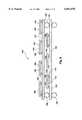
- FIG. 1illustrates a first stacked assembly 100 of the present invention.
- the stacked assembly 100comprises a base substrate 102 having a first surface 104 with a plurality of bond pads 106 disposed thereon and a second surface 108 with a plurality of bond pads 110 disposed thereon.
- Each of the base substrate first surface bond pads 106is in electrical communication with its respective base substrate second surface bond pad 110 via a plurality of lead traces 112 extending through the base substrate 102.
- a plurality of electric connections 114extends from the base substrate first surface bond pads 106.
- the base substrate electric connections 114make contact with the other components or substrates.
- the stacked assembly 100further includes a first stacked substrate 116 having a first surface 118 with a plurality of bond pads 120 and a second surface 122 with a plurality of bond pads 124 disposed thereon.
- the first stacked substrate 116is in electrical communication with the base substrate second surface 108 via a plurality of first electric connections 126.
- the first electric connections 126extend between each first stacked substrate first surface bond pad 120 and its respective base substrate second surface bond pad 110.
- the bond pads of both the first stacked substrate 116 and base substrate 102are preferably located such that each respective bond pad pair aligns perpendicularly.
- a plurality of first semiconductor dice 128 each having a face side 130 and a back side 132is attached to each of the first stacked substrate first surface 118 and the first stacked substrate second surface 122 with a first layer of adhesive 134 applied to the first semiconductor die back sides 132.
- the first semiconductor dice 128are in electrical contact with a plurality of first stacked substrate electrical traces 136 via TAB bonds 138.
- the first stacked substrate electrical traces 136extend in or on the first stacked substrate 116 and may contact the first stacked substrate first surface bond pad 120, the first stacked substrate second surface bond pad 124, and/or another first semiconductor die 128.
- the stacked assembly 100still further includes a second stacked substrate 140 having a first surface 142 with a plurality of bond pads 144 thereon and a second surface 146.
- the second stacked substrate 140is in electrical communication with the first stacked substrate second surface 122 via a plurality of second electric connections 148.
- the second electric connections 148extend between each second stacked substrate first surface bond pad 144 and its respective first stacked substrate second surface bond pad 124.
- the bond pads of both the second stacked substrate 140 and first stacked substrate 116are preferably located such that each respective bond pad pair aligns perpendicularly.
- a plurality of second semiconductor dice 150 each having a face side 152 and a back side 154is attached to the second stacked substrate first surface 142 with a second layer of adhesive 156 applied to the second semiconductor die back sides 154.
- the second semiconductor dice 150are in electrical contact with a plurality of second stacked substrate electrical traces 158 via wirebonds 160.
- a plurality of third semiconductor dice 162 each having a face side 164is attached to the second stacked substrate second surface 146 with a plurality of flip chip contacts 166, such as BGA, PGA or the like.
- the flip chip contacts 166are in electrical contact with the second stacked substrate electrical traces 158.
- the second stacked substrate electrical traces 158extend in or on the second stacked substrate 140 and may contact the second stacked substrate first surface bond pads 144, the second semiconductor dice 150 and/or another third semiconductor die 162.
- a flip chip dielectric material 168may be disposed between the third semiconductor dice face side 164 and the second stacked substrate second surface 146. Additionally, a dielectric material 170 may be disposed between the base substrate 102 and the first stacked substrate 116, and/or the first stacked substrate 116 and the second stack substrate 140. Furthermore, an encapsulation material 172 may cover the stack dice portion of the stacked assembly 100.
- any available substrate surfacesuch as the base substrate second surface 108, may have semiconductor dice attached thereto.
- FIG. 2illustrates a substrate assembly 200 having a uniform bond pad arrangement, such as shown as the first surface 142 of the second stacked substrate 140 in FIG. 1.
- the substrate assembly 200comprises a substrate 202 with a plurality of bond pads 204 distributed about a periphery 206 of a surface 208 of the substrate 202.
- a plurality of semiconductor dice 210is disposed on the substrate surface 208 within the bond pads 204.
- the semiconductor dice 210have a face side 212 and a back side 214.
- the semiconductor dice 210are attached by an adhesive layer 216 applied to the semiconductor dice back side 214 and make electrical contact with the substrate surface 208 by a plurality of bond wires 218.
- Such an arrangement of bond pads 204yields a strong, well-supported structure.
- FIG. 3illustrates a substrate assembly 300 having a non-uniform bond pad arrangement.
- the substrate assembly 300comprises a substrate 302 with a plurality of bond pads 304 distributed in a non-uniform pattern across a surface 306 of the substrate 302.
- a plurality of semiconductor dice 308is disposed on the substrate surface 306.
- the semiconductor dice 308have a face side 310 and a back side 312.
- the semiconductor dice 308are attached by an adhesive layer 314 applied to the semiconductor dice back side 312 and make electrical contact with the substrate surface 306 by a plurality of bond wires 316.
- FIG. 4illustrates a variable stack size assembly 400 of the present invention.
- the variable stack size assembly 400comprises a first stacked substrate 402 having a surface 404 with a plurality of first bond pads 406 and second bond pads 408 disposed thereon.
- a plurality of first semiconductor dice 410each having a face side 412 and a back side 414 is attached to the first stacked substrate surface 404 with a first layer of dielectric adhesive 416 applied to the first semiconductor die back sides 414.
- the first semiconductor dice 410are in electric communication with a plurality of first stacked substrate electrical traces (not shown) via wirebonds 418.
- the variable stack size assembly 400further includes a first small stacked substrate 420 having a first surface 422 with a plurality of bond pads 424 disposed thereon and a second surface 426.
- the first small stacked substrate 420is in electrical communication with the first stacked substrate surface 404 via a plurality of first small stacked substrate electric connections 428.
- the first small stacked substrate electric connections 428extend between each first stacked substrate surface first bond pad 406 and its respective first small stacked substrate first surface bond pad 424.
- the bond pads of both the first stacked substrate 402 and first small stacked substrate 420are preferably located such that each respective bond pad pair aligns perpendicularly.
- At least one second semiconductor die 430 having a face side 434 and a back side 432is attached to the first small stacked substrate second surface 426 with a second layer of dielectric adhesive 436.
- the second semiconductor die 430is in electric communication with a plurality of first small stacked substrate electrical traces (not shown) via wirebonds 438.
- the variable stack size assembly 400still further includes a second stacked substrate 440 having a first surface 442 with a plurality of bond pads 444 thereon and a second surface 446 with a plurality of bond pads 448.
- the second stacked substrate 440is in electrical communication with the first stacked substrate surface 404 via a plurality of first electric connections 450.
- the first electric connections 450extend between each second stacked substrate first surface bond pad 444 and its respective first stacked substrate second surface bond pad 408.
- the bond pads of both the second stacked substrate 440 and first stacked substrate 402are preferably located such that each respective bond pad pair aligns perpendicularly.
- a plurality of third semiconductor dice 452 each having a face side 454 and a back side 456is attached to the second stacked substrate second surface 446 with a third layer of dielectric adhesive 458 applied to the third semiconductor die back sides 456.
- the third semiconductor dice 452are in electric communication with a plurality of second stacked substrate electrical traces (not shown) via wirebonds 460.
- the variable stack size assembly 400still further includes a third stacked substrate 462 having a first surface 464 with a plurality of bond pads 466 thereon and a second surface 468 with a plurality of bond pads 470 thereon.
- the third stacked substrate 462is in electrical communication with the second stacked substrate second surface 446 via a plurality of second electric connections 472.
- the second electric connections 472extend between each third stacked substrate first surface bond pad 466 and its respective second stacked substrate second surface bond pad 448.
- the bond pads of both the third stacked substrate 462 and second stacked substrate 440are preferably located such that each respective bond pad pair aligns perpendicularly.
- a plurality of fourth semiconductor dice 474 each having a face side 476 and a back side 478is attached to the third stacked substrate first surface 464 with a fourth layer of dielectric adhesive 480 applied to the fourth semiconductor die back sides 478.
- the fourth semiconductor dice 474are in electrical contact with a plurality of third stacked substrate electrical traces (not shown) via wirebonds 482.
- a plurality of fifth semiconductor dice 484 each having a face side 486 and a back side 488is attached to the third stacked substrate second surface 468 with a fifth layer of dielectric adhesive 490 applied to the fifth semiconductor die back sides 488.
- the fifth semiconductor dice 484are in electric communication with a plurality of third stacked substrate electrical traces (not shown) via wirebonds 492.
- the variable stack size assembly 400further includes a second small stacked substrate 494 having a first surface 496 with a plurality of bond pads 498 disposed thereon and a second surface 500.
- the second small stacked substrate 494is in electrical communication with the third substrate second surface 468 via a plurality of second small substrate electric connections 502.
- the second small substrate electric connections 502extend between each second small stacked substrate first surface bond pad 498 and its respective third stacked substrate second surface bond pad 470.
- the bond pads of both the second small stacked substrate 494 and third stacked substrate 462are preferably located such that each respective bond pad pair aligns perpendicularly.
- At least one sixth semiconductor die 504 having a face side 506 and a back side 508is attached to the second small stacked substrate first surface 496 with a sixth layer of dielectric adhesive 510.
- the sixth semiconductor die 504is in electric communication with a plurality of second small stacked substrate electrical traces (not shown) via wirebonds 512.
- At least one seventh semiconductor die 514 having a face side 516 and a back side 518is attached to the second small stacked substrate second surface 500 with a seventh layer of dielectric adhesive 520.
- the seventh semiconductor die 514is in electric communication with a plurality of second small stacked substrate electrical traces (not shown) via wirebonds 522.
- FIG. 5illustrates a substrate assembly 600 having a smaller substrate 602 on a larger substrate 604, such as shown as third stacked substrate 462 and second small stacked substrate 494 in FIG. 4.
- the substrate assembly 600comprises the larger substrate 604 having a plurality of first semiconductor dice 606 and the smaller substrate 602 disposed on a surface 608 of the larger substrate 604.
- the first semiconductor dice 606have a face side 612 and a back side 614.
- the first semiconductor dice 606are attached by a first layer of adhesive 616 applied to the semiconductor dice back side 614 and make electrical contact with the substrate surface 608 by a plurality of first bond wires 618.
- the smaller substrate 602has a first surface 620 and a second surface 622.
- the smaller substrate 602has a plurality of electrical contacts 624 extending between a plurality of bond pads 626 on the smaller substrate first surface 620 and a plurality of bond pads 628 on the larger substrate surface 608.
- a plurality of second semiconductor dice 630(only one shown) is disposed on the smaller substrate second surface 622.
- the second semiconductor dice 630have a face side 634 and a back side 636.
- the second semiconductor dice 630are attached by a second layer of adhesive 638 applied to the second semiconductor dice back side 636 and make electrical contact with the smaller substrate second surface 622 by a plurality of bond wires 640.
- the electrical traces of the smaller substratehave not been illustrated, it is understood that electrical traces make electrical connections in the same manner as described for FIG. 1.
- FIG. 6illustrates a substrate assembly 700 having a plurality of semiconductor devices mounted on substrates using known flip chip attachment techniques.
- the substrate assembly 700comprises a first substrate 704 having a plurality of first semiconductor dice 702 disposed thereon and a second substrate 708 having a plurality of second semiconductor dice 706 disposed thereon.
- the first semiconductor dice 702each have a surface or face side 710 having a plurality of bond pads (not shown) thereon and a back side 712.
- the first semiconductor dice 702make electrical contact with the traces (not shown) on the first substrate surface 714 by a plurality of first conductive material balls 716 extending between the bond pads (not shown) on the face surface 710 of the dice 702 and the traces (not shown) on the first substrate surface 714.
- the balls 716may be made of any suitable conductive material to connect the semiconductor dice 702 to the conductive traces on first substrate 704, such as solder, conductive epoxy, etc.
- the balls 716are shown as generally spherical in shape, although they may be any suitable geometric shape and size for bonding purposes. Further, z-axis connectors may be substituted for the balls 716 if so desired.
- the second substrate 708has a surface 718 having a plurality of conductive traces (not shown) thereon.
- the second plurality of semiconductor dice 706each have a face side 720 having a plurality of bond pads (not shown) thereon and a back side 722.
- the second plurality of semiconductor dice 706make electrical contact with the second substrate surface 718 by a plurality of second conductive material balls 724 extending between the bond pads of the dice 706 and the conductive traces on the second substrate surface 718.
- the balls 724may be made of any suitable conductive material to connect the semiconductor dice 706 to the conductive traces on second substrate 708, such as solder, conductive epoxy, etc.
- the balls 724are shown as generally spherical in shape, although they may be any suitable geometric shape and size for bonding purposes. Further, z-axis connectors may be substituted for balls 724 if so desired.
- the desired conductive traces on the surface 714 of the first substrate 704are connected to the desired conductive traces on the surface 718 of the second substrate 708 by larger conductive balls 726.
- the larger conductive balls 726may be of any suitable conductive material, such as solder, conductive epoxy, etc.
- the larger conductive ballsare also used for connecting the surface 728 of the first substrate 704 to any other desired substrate. Further, z-axis connectors may be substituted for balls 726 if so desired. It should be understood that the conductive traces which have only been referred to on the surfaces 714 and 718 of the substrates may be formed on either side of the first substrate 704 or the second substrate 708 and, as such, have not been illustrated.
- any connectors extending through the first substrate 704 and second substrate 708 for connection purposeshave not been shown.
- the bond pads on the first semiconductor dice 702 and second semiconductor dice 706have not been illustrated.
- the first semiconductor dice 702are attached to the first substrate 704 and the second semiconductor dice 706 are attached to the second substrate 708 by well known flip-chip bonding techniques, depending upon the type of conductive balls 716 and 724 used for connection purposes.
- the smaller stacked substratesi.e., first small stacked substrate 420 and second small stacked substrate 494 of FIG. 4, and smaller substrate 602 of FIG. 5
- the larger substratesi.e., first stacked substrate 402 and third stacked substrate 462 of FIG. 4, larger substrate 604 of FIG. 5 or first semiconductor dice 702 stacked on first substrate 704 and second semiconductor devices 706 stacked on second substrate 708 of FIG. 6
- the combination of these example componentscould constitute a complete component.
- the embodiments shown in FIGS. 4, 5 and 6could include electric connections (such as electric connections 114 of FIG. 1) to connect to other components or other substrates.
Landscapes
- Engineering & Computer Science (AREA)
- Microelectronics & Electronic Packaging (AREA)
- Power Engineering (AREA)
- Physics & Mathematics (AREA)
- Condensed Matter Physics & Semiconductors (AREA)
- General Physics & Mathematics (AREA)
- Computer Hardware Design (AREA)
- Manufacturing & Machinery (AREA)
- Wire Bonding (AREA)
Abstract
Description
Claims (32)
Priority Applications (5)
| Application Number | Priority Date | Filing Date | Title |
|---|---|---|---|
| US09/233,997US6051878A (en) | 1997-03-10 | 1999-01-19 | Method of constructing stacked packages |
| US09/466,454US6222265B1 (en) | 1997-03-10 | 1999-12-17 | Method of constructing stacked packages |
| US09/834,706US6404044B2 (en) | 1997-03-10 | 2001-04-13 | Semiconductor package with stacked substrates and multiple semiconductor dice |
| US10/137,584US6583503B2 (en) | 1997-03-10 | 2002-05-02 | Semiconductor package with stacked substrates and multiple semiconductor dice |
| US10/600,232US6979895B2 (en) | 1997-03-10 | 2003-06-19 | Semiconductor assembly of stacked substrates and multiple semiconductor dice |
Applications Claiming Priority (2)
| Application Number | Priority Date | Filing Date | Title |
|---|---|---|---|
| US08/813,467US5994166A (en) | 1997-03-10 | 1997-03-10 | Method of constructing stacked packages |
| US09/233,997US6051878A (en) | 1997-03-10 | 1999-01-19 | Method of constructing stacked packages |
Related Parent Applications (1)
| Application Number | Title | Priority Date | Filing Date |
|---|---|---|---|
| US08/813,467DivisionUS5994166A (en) | 1997-03-10 | 1997-03-10 | Method of constructing stacked packages |
Related Child Applications (1)
| Application Number | Title | Priority Date | Filing Date |
|---|---|---|---|
| US09/466,454ContinuationUS6222265B1 (en) | 1997-03-10 | 1999-12-17 | Method of constructing stacked packages |
Publications (1)
| Publication Number | Publication Date |
|---|---|
| US6051878Atrue US6051878A (en) | 2000-04-18 |
Family
ID=25212451
Family Applications (6)
| Application Number | Title | Priority Date | Filing Date |
|---|---|---|---|
| US08/813,467Expired - LifetimeUS5994166A (en) | 1997-03-10 | 1997-03-10 | Method of constructing stacked packages |
| US09/233,997Expired - LifetimeUS6051878A (en) | 1997-03-10 | 1999-01-19 | Method of constructing stacked packages |
| US09/466,454Expired - LifetimeUS6222265B1 (en) | 1997-03-10 | 1999-12-17 | Method of constructing stacked packages |
| US09/834,706Expired - LifetimeUS6404044B2 (en) | 1997-03-10 | 2001-04-13 | Semiconductor package with stacked substrates and multiple semiconductor dice |
| US10/137,584Expired - LifetimeUS6583503B2 (en) | 1997-03-10 | 2002-05-02 | Semiconductor package with stacked substrates and multiple semiconductor dice |
| US10/600,232Expired - Fee RelatedUS6979895B2 (en) | 1997-03-10 | 2003-06-19 | Semiconductor assembly of stacked substrates and multiple semiconductor dice |
Family Applications Before (1)
| Application Number | Title | Priority Date | Filing Date |
|---|---|---|---|
| US08/813,467Expired - LifetimeUS5994166A (en) | 1997-03-10 | 1997-03-10 | Method of constructing stacked packages |
Family Applications After (4)
| Application Number | Title | Priority Date | Filing Date |
|---|---|---|---|
| US09/466,454Expired - LifetimeUS6222265B1 (en) | 1997-03-10 | 1999-12-17 | Method of constructing stacked packages |
| US09/834,706Expired - LifetimeUS6404044B2 (en) | 1997-03-10 | 2001-04-13 | Semiconductor package with stacked substrates and multiple semiconductor dice |
| US10/137,584Expired - LifetimeUS6583503B2 (en) | 1997-03-10 | 2002-05-02 | Semiconductor package with stacked substrates and multiple semiconductor dice |
| US10/600,232Expired - Fee RelatedUS6979895B2 (en) | 1997-03-10 | 2003-06-19 | Semiconductor assembly of stacked substrates and multiple semiconductor dice |
Country Status (1)
| Country | Link |
|---|---|
| US (6) | US5994166A (en) |
Cited By (119)
| Publication number | Priority date | Publication date | Assignee | Title |
|---|---|---|---|---|
| US6208526B1 (en)* | 1999-07-23 | 2001-03-27 | Motorola, Inc. | Mounting multiple substrate frame and leadless surface mountable assembly using same |
| US6222265B1 (en)* | 1997-03-10 | 2001-04-24 | Micron Technology, Inc. | Method of constructing stacked packages |
| US6240634B1 (en)* | 1997-09-12 | 2001-06-05 | Fujitsu Limited | Method of producing a multichip package module in which rough-pitch and fine-pitch chips are mounted on a board |
| US6287892B1 (en)* | 1997-04-17 | 2001-09-11 | Nec Corporation | Shock-resistant semiconductor device and method for producing same |
| US6426559B1 (en) | 2000-06-29 | 2002-07-30 | National Semiconductor Corporation | Miniature 3D multi-chip module |
| US6441483B1 (en) | 2001-03-30 | 2002-08-27 | Micron Technology, Inc. | Die stacking scheme |
| US20030006496A1 (en)* | 2001-03-15 | 2003-01-09 | Venkateshwaran Vaiyapuri | Semiconductor/printed circuit board assembly, and computer system |
| US6528408B2 (en) | 2001-05-21 | 2003-03-04 | Micron Technology, Inc. | Method for bumped die and wire bonded board-on-chip package |
| US6537852B2 (en) | 2001-08-22 | 2003-03-25 | International Business Machines Corporation | Spacer - connector stud for stacked surface laminated multichip modules and methods of manufacture |
| US6548376B2 (en) | 2001-08-30 | 2003-04-15 | Micron Technology, Inc. | Methods of thinning microelectronic workpieces |
| US20030071338A1 (en)* | 2001-10-16 | 2003-04-17 | Jeung Boon Suan | Apparatus and method for leadless packaging of semiconductor devices |
| US6552910B1 (en) | 2000-06-28 | 2003-04-22 | Micron Technology, Inc. | Stacked-die assemblies with a plurality of microelectronic devices and methods of manufacture |
| US6560117B2 (en) | 2000-06-28 | 2003-05-06 | Micron Technology, Inc. | Packaged microelectronic die assemblies and methods of manufacture |
| US20030102546A1 (en)* | 2001-04-17 | 2003-06-05 | Lee Teck Kheng | Method and apparatus for package reduction in stacked chip and board assemblies |
| US20030104654A1 (en)* | 2000-06-28 | 2003-06-05 | Farnworth Warren M. | Recessed encapsulated microelectronic devices and methods for formation |
| US20030137042A1 (en)* | 2001-06-21 | 2003-07-24 | Mess Leonard E. | Stacked mass storage flash memory package |
| US20030137041A1 (en)* | 2002-01-24 | 2003-07-24 | International Business Machines Corporation | Vertically stacked memory chips in FBGA packages |
| US20030141596A1 (en)* | 2000-02-28 | 2003-07-31 | Hidehiro Nakamura | Wiring board, semiconductor device, and method of manufacturing wiring board |
| US20030151135A1 (en)* | 2000-01-31 | 2003-08-14 | Noriaki Sakamoto | Circuit device and manufacturing method of circuit device |
| US6607937B1 (en) | 2000-08-23 | 2003-08-19 | Micron Technology, Inc. | Stacked microelectronic dies and methods for stacking microelectronic dies |
| US20030160317A1 (en)* | 2000-01-31 | 2003-08-28 | Noriaki Sakamoto | Circuit device and manufacturing method of circuit device and semiconductor module |
| US20030162325A1 (en)* | 2002-01-09 | 2003-08-28 | Micron Technology, Inc. | Stacked die in die BGA package |
| US6617700B2 (en)* | 2000-08-11 | 2003-09-09 | Samsung Electronics Co., Ltd, | Repairable multi-chip package and high-density memory card having the package |
| US20030183930A1 (en)* | 2001-07-04 | 2003-10-02 | Hiroyuki Fukasawa | Semiconductor device and semiconductor module |
| US6670701B2 (en)* | 2001-02-01 | 2003-12-30 | Mitsubishi Denki Kabushiki Kaisha | Semiconductor module and electronic component |
| US20040023436A1 (en)* | 2001-09-17 | 2004-02-05 | Megic Corporation | Structure of high performance combo chip and processing method |
| US20040026773A1 (en)* | 2002-08-08 | 2004-02-12 | Koon Eng Meow | Packaged microelectronic components |
| US20040038447A1 (en)* | 2002-08-21 | 2004-02-26 | Corisis David J | Packaged microelectronic devices and methods for assembling microelectronic devices |
| US20040043675A1 (en)* | 2002-08-29 | 2004-03-04 | Micron Technology, Inc. | Multi-component integrated circuit contacts |
| US6706557B2 (en) | 2001-09-21 | 2004-03-16 | Micron Technology, Inc. | Method of fabricating stacked die configurations utilizing redistribution bond pads |
| US6710454B1 (en) | 2000-02-16 | 2004-03-23 | Micron Technology, Inc. | Adhesive layer for an electronic apparatus having multiple semiconductor devices |
| US6734538B1 (en) | 2001-04-12 | 2004-05-11 | Bae Systems Information & Electronic Systems Integration, Inc. | Article comprising a multi-layer electronic package and method therefor |
| US20040100772A1 (en)* | 2002-11-22 | 2004-05-27 | Chye Lim Thiam | Packaged microelectronic component assemblies |
| US6750547B2 (en) | 2001-12-26 | 2004-06-15 | Micron Technology, Inc. | Multi-substrate microelectronic packages and methods for manufacture |
| US6774473B1 (en)* | 1999-07-30 | 2004-08-10 | Ming-Tung Shen | Semiconductor chip module |
| US20040173899A1 (en)* | 2003-03-04 | 2004-09-09 | Peng Neo Chee | Microelectronic component assemblies employing lead frames having reduced-thickness inner lengths |
| US20040178495A1 (en)* | 2003-03-14 | 2004-09-16 | Yean Tay Wuu | Microelectronic devices and methods for packaging microelectronic devices |
| US20040195668A1 (en)* | 2003-02-06 | 2004-10-07 | Toshihiro Sawamoto | Semiconductor device, electronic device, electronic equipment, method of manufacturing semiconductor device, and method of manufacturing electronic device |
| US20040212082A1 (en)* | 2000-09-21 | 2004-10-28 | Jicheng Yang | Method to prevent die attach adhesive contamination in stacked chips |
| US20040217380A1 (en)* | 2003-02-25 | 2004-11-04 | Akiyoshi Aoyagi | Semiconductor device, electronic device, electronic apparatus, method for manufacturing a semiconductor device, and method for manufacturing an electronic device |
| US20040222510A1 (en)* | 2003-03-24 | 2004-11-11 | Akiyoshi Aoyagi | Semiconductor device, semiconductor pack age, electronic device, electronic apparatus, and manufacturing methods of semiconductor device and electronic device |
| US20040222519A1 (en)* | 2003-03-18 | 2004-11-11 | Akiyoshi Aoyagi | Semiconductor device, electronic device, electronic apparatus, method of manufacturing semiconductor device, and method of manufacturing electronic device |
| US20040222534A1 (en)* | 2003-02-07 | 2004-11-11 | Toshihiro Sawamoto | Semiconductor device, electronic device, electronic equipment, method of manufacturing semiconductor device, and method of manufacturing electronic device |
| US20040227236A1 (en)* | 2003-03-17 | 2004-11-18 | Toshihiro Sawamoto | Semiconductor device, electronic device, electronic apparatus, and methods for manufacturing carrier substrate, semiconductor device, and electronic device |
| US20040238948A1 (en)* | 2003-03-25 | 2004-12-02 | Masakuni Shiozawa | Semiconductor device, electronic device, electronic apparatus, and method of manufacturing semiconductor device |
| US20050019984A1 (en)* | 2000-08-09 | 2005-01-27 | Tongbi Jiang | Multiple substrate microelectronic devices and methods of manufacture |
| US20050026327A1 (en)* | 2002-04-15 | 2005-02-03 | Micron Technology, Inc. | Semiconductor integrated circuit package having electrically disconnected solder balls for mounting |
| US20050026415A1 (en)* | 2002-01-16 | 2005-02-03 | Micron Technology, Inc. | Fabrication of stacked microelectronic devices |
| US20050023655A1 (en)* | 2001-08-29 | 2005-02-03 | Fee Setho Sing | Packaged microelectronic devices and methods of forming same |
| US20050045378A1 (en)* | 2003-08-29 | 2005-03-03 | Heng Mung Suan | Stacked microfeature devices and associated methods |
| KR100480437B1 (en)* | 2002-10-24 | 2005-04-07 | 삼성전자주식회사 | Semiconductor chip package stacked module |
| US20050104228A1 (en)* | 2003-11-13 | 2005-05-19 | Rigg Sidney B. | Microelectronic devices, methods for forming vias in microelectronic devices, and methods for packaging microelectronic devices |
| US20050104171A1 (en)* | 2003-11-13 | 2005-05-19 | Benson Peter A. | Microelectronic devices having conductive complementary structures and methods of manufacturing microelectronic devices having conductive complementary structures |
| US20050110166A1 (en)* | 2003-03-18 | 2005-05-26 | Akiyoshi Aoyagi | Semiconductor device, electronic device, electronic apparatus, method of manufacturing semiconductor device, and method of manufacturing electronic device |
| US20050127478A1 (en)* | 2003-12-10 | 2005-06-16 | Hiatt William M. | Microelectronic devices and methods for filling vias in microelectronic devices |
| US20050189623A1 (en)* | 2001-03-12 | 2005-09-01 | Salman Akram | Multiple die package |
| US20060035503A1 (en)* | 2003-08-29 | 2006-02-16 | Seng Eric T S | Invertible microfeature device packages and associated methods |
| US20060043534A1 (en)* | 2004-08-26 | 2006-03-02 | Kirby Kyle K | Microfeature dies with porous regions, and associated methods and systems |
| US20060044773A1 (en)* | 2004-08-25 | 2006-03-02 | Micron Technology, Inc. | Methods and apparatuses for transferring heat from stacked microfeature devices |
| US7037756B1 (en) | 2001-08-30 | 2006-05-02 | Micron Technology, Inc. | Stacked microelectronic devices and methods of fabricating same |
| US20060151206A1 (en)* | 2005-01-13 | 2006-07-13 | Sharp Kabushiki Kaisha | Semiconductor device and manufacturing method therefor |
| US20060177970A1 (en)* | 2005-02-08 | 2006-08-10 | Micron Technology, Inc. | Methods of Adhering Microfeature Workpieces, Including A Chip, To A Support Member |
| US20060186523A1 (en)* | 2005-02-21 | 2006-08-24 | Shu-Hua Hu | Chip-type micro-connector and method of packaging the same |
| US20060231927A1 (en)* | 2003-05-15 | 2006-10-19 | Kumamoto Technology & Industry Foundation | Semiconductor chip mounting body and manufacturing method thereof |
| US20060292858A1 (en)* | 2002-07-18 | 2006-12-28 | Micron Technology, Inc. | Techniques to create low K ILD for beol |
| US20070013081A1 (en)* | 2005-07-14 | 2007-01-18 | Samsung Electro-Mechanics Co., Ltd. | Electronic module with stacked ic chip structure |
| US20070018337A1 (en)* | 2002-04-04 | 2007-01-25 | Micron Technology, Inc. | Method and apparatus for attaching microelectronic substrates and support members |
| US7180171B1 (en) | 2004-01-08 | 2007-02-20 | Smart Modular Technologies, Inc. | Single IC packaging solution for multi chip modules |
| US20070045807A1 (en)* | 2005-09-01 | 2007-03-01 | Micron Technology, Inc. | Microelectronic devices and methods for manufacturing microelectronic devices |
| US20070045803A1 (en)* | 2005-08-26 | 2007-03-01 | Micron Technology, Inc. | Microelectronic device packages, stacked microelectronic device packages, and methods for manufacturing microelectronic devices |
| US20070045797A1 (en)* | 2005-08-24 | 2007-03-01 | Micron Technology, Inc. | Microelectronic devices and microelectronic support devices, and associated assemblies and methods |
| US20070045796A1 (en)* | 2005-08-19 | 2007-03-01 | Micron Technology, Inc. | Microelectronic devices, stacked microelectronic devices, and methods for manufacturing microelectronic devices |
| US20070045872A1 (en)* | 2005-08-31 | 2007-03-01 | Fee Setho S | Microelectronic devices having intermediate contacts for connection to interposer substrates, and associated methods of packaging microelectronic devices with intermediate contacts |
| US20070045875A1 (en)* | 2005-08-30 | 2007-03-01 | Micron Technology, Inc. | Methods for wafer-level packaging of microfeature devices and microfeature devices formed using such methods |
| US20070045862A1 (en)* | 2005-09-01 | 2007-03-01 | Micron Technology, Inc. | Stacked microelectronic devices and methods for manufacturing microelectronic devices |
| US7198693B1 (en) | 2002-02-20 | 2007-04-03 | Micron Technology, Inc. | Microelectronic device having a plurality of stacked dies and methods for manufacturing such microelectronic assemblies |
| US20070080441A1 (en)* | 2005-08-18 | 2007-04-12 | Scott Kirkman | Thermal expansion compensation graded IC package |
| US20070096265A1 (en)* | 2005-11-01 | 2007-05-03 | Sandisk Corporation | Multiple die integrated circuit package |
| US7217597B2 (en) | 2004-06-22 | 2007-05-15 | Micron Technology, Inc. | Die stacking scheme |
| US20070136766A1 (en)* | 2005-12-09 | 2007-06-14 | Ryuichi Iwamura | Cross-phase adapter for powerline communications (PLC) network |
| US20070148820A1 (en)* | 2005-12-22 | 2007-06-28 | Micron Technology, Inc. | Microelectronic devices and methods for manufacturing microelectronic devices |
| US20070155048A1 (en)* | 2005-12-29 | 2007-07-05 | Micron Technology, Inc. | Methods for packaging microelectronic devices and microelectronic devices formed using such methods |
| US20070165390A1 (en)* | 2005-12-02 | 2007-07-19 | Samsung Electronics Co., Ltd. | Printed circuit board |
| US20070181989A1 (en)* | 2006-02-08 | 2007-08-09 | Micron Technology, Inc. | Microelectronic devices, stacked microelectronic devices, and methods for manufacturing such devices |
| US20070210447A1 (en)* | 2006-03-07 | 2007-09-13 | Kinsley Thomas H | Elongated fasteners for securing together electronic components and substrates, semiconductor device assemblies including such fasteners, and accompanying systems and methods |
| US20070210441A1 (en)* | 2006-03-08 | 2007-09-13 | Micron Technology, Inc. | Microelectronic device assemblies including assemblies with recurved leadframes, and associated methods |
| US20070228577A1 (en)* | 2006-03-29 | 2007-10-04 | Micron Technology, Inc. | Packaged microelectronic devices recessed in support member cavities, and associated methods |
| US20070240083A1 (en)* | 2006-03-28 | 2007-10-11 | Toshiyuki Hiroi | Processing apparatus |
| US20070262436A1 (en)* | 2006-05-12 | 2007-11-15 | Micron Technology, Inc. | Microelectronic devices and methods for manufacturing microelectronic devices |
| US20080012110A1 (en)* | 2006-07-17 | 2008-01-17 | Micron Technology, Inc. | Microelectronic packages with leadframes, including leadframes configured for stacked die packages, and associated systems and methods |
| US20080048316A1 (en)* | 2006-08-25 | 2008-02-28 | Micron Technology, Inc. | Packaged microdevices and methods for manufacturing packaged microdevices |
| US20080050859A1 (en)* | 2005-11-01 | 2008-02-28 | Sandisk Corporation | Methods for a multiple die integrated circuit package |
| US7365424B2 (en) | 2004-07-23 | 2008-04-29 | Micron Technology, Inc. | Microelectronic component assemblies with recessed wire bonds and methods of making same |
| US20080128900A1 (en)* | 2006-12-04 | 2008-06-05 | Micron Technology, Inc. | Packaged microelectronic devices and methods for manufacturing packaged microelectronic devices |
| US20080142942A1 (en)* | 2006-12-19 | 2008-06-19 | Yong Du | Method and apparatus for multi-chip packaging |
| US20080150113A1 (en)* | 2006-12-21 | 2008-06-26 | Tessera, Inc. | Enabling uniformity of stacking process through bumpers |
| US20080165517A1 (en)* | 2007-01-05 | 2008-07-10 | Wang Erik L | Multiple circuit board arrangements in electronic devices |
| US20080224291A1 (en)* | 2007-03-13 | 2008-09-18 | Micron Technology, Inc. | Packaged semiconductor components having substantially rigid support members and methods of packaging semiconductor components |
| US20090014897A1 (en)* | 2003-05-15 | 2009-01-15 | Kumamoto Technology & Industry Foundation | Semiconductor chip package and method of manufacturing the same |
| US20090026600A1 (en)* | 2007-07-24 | 2009-01-29 | Micron Technology, Inc. | Microelectronic die packages with metal leads, including metal leads for stacked die packages, and associated systems and methods |
| US20090045489A1 (en)* | 2007-08-16 | 2009-02-19 | Micron Technology, Inc. | Microelectronic die packages with leadframes, including leadframe-based interposer for stacked die packages, and associated systems and methods |
| US20090067143A1 (en)* | 2007-09-07 | 2009-03-12 | Jung-Do Lee | Electronic device having stack-type semiconductor package and method of forming the same |
| US20090179318A1 (en)* | 2008-01-10 | 2009-07-16 | Abounion Technology Corporation | Multi-channel stackable semiconductor device and method for fabricating the same, and stacking substrate applied to the semiconductor device |
| US20090206455A1 (en)* | 2008-02-19 | 2009-08-20 | Texas Instruments Incorporated | Integrated circuit stacked package precursors and stacked packaged devices and systems therefrom |
| US20100059897A1 (en)* | 2008-09-11 | 2010-03-11 | Micron Technology, Inc. | Interconnect structures for stacked dies, including penetrating structures for through-silicon vias, and associated systems and methods |
| US20100149745A1 (en)* | 2008-12-17 | 2010-06-17 | Samsung Electronics Co., Ltd. | Installing structure of memory for portable terminal |
| US20100213596A1 (en)* | 2009-02-25 | 2010-08-26 | Hynix Semiconductor Inc. | Stack package |
| US20110062597A1 (en)* | 2007-01-02 | 2011-03-17 | Taiwan Semiconductor Manufacturing Co., Ltd. | Package structures |
| US20110272798A1 (en)* | 2010-05-06 | 2011-11-10 | Hynix Semiconductor Inc. | Chip unit and stack package having the same |
| US20120061775A1 (en)* | 2010-09-10 | 2012-03-15 | Woojin Kim | Device for use as dual-sided sensor package |
| US20140203443A1 (en)* | 2009-03-17 | 2014-07-24 | Stats Chippac, Ltd. | Semiconductor Device and Method of Providing Z-Interconnect Conductive Pillars with Inner Polymer Core |
| US20140319702A1 (en)* | 2007-06-29 | 2014-10-30 | Stats Chippac, Ltd. | Stackable Package by Using Internal Stacking Modules |
| US9603252B1 (en) | 2013-11-12 | 2017-03-21 | Smart Modular Technologies, Inc. | Integrated circuit device system with elevated configuration and method of manufacture thereof |
| US9648754B1 (en)* | 2013-11-12 | 2017-05-09 | Smart Modular Technologies, Inc. | Integrated circuit device system with elevated stacked configuration and method of manufacture thereof |
| US20180042110A1 (en)* | 2016-08-04 | 2018-02-08 | X-Celeprint Limited | Printable 3d electronic structure |
| US20180068938A1 (en)* | 2008-09-06 | 2018-03-08 | Broadpak Corporation | Scalable semiconductor interposer integration |
| US10796971B2 (en) | 2018-08-13 | 2020-10-06 | X Display Company Technology Limited | Pressure-activated electrical interconnection with additive repair |
| US11302617B2 (en)* | 2008-09-06 | 2022-04-12 | Broadpak Corporation | Scalable semiconductor interposer integration |
| US11387178B2 (en)* | 2020-03-06 | 2022-07-12 | X-Celeprint Limited | Printable 3D electronic components and structures |
Families Citing this family (336)
| Publication number | Priority date | Publication date | Assignee | Title |
|---|---|---|---|---|
| US5148265A (en) | 1990-09-24 | 1992-09-15 | Ist Associates, Inc. | Semiconductor chip assemblies with fan-in leads |
| US6861290B1 (en) | 1995-12-19 | 2005-03-01 | Micron Technology, Inc. | Flip-chip adaptor package for bare die |
| JPH10270496A (en)* | 1997-03-27 | 1998-10-09 | Hitachi Ltd | Electronic device, information processing device, semiconductor device, and semiconductor chip mounting method |
| US6551857B2 (en)* | 1997-04-04 | 2003-04-22 | Elm Technology Corporation | Three dimensional structure integrated circuits |
| US6525414B2 (en)* | 1997-09-16 | 2003-02-25 | Matsushita Electric Industrial Co., Ltd. | Semiconductor device including a wiring board and semiconductor elements mounted thereon |
| JP2000208698A (en)* | 1999-01-18 | 2000-07-28 | Toshiba Corp | Semiconductor device |
| US6150724A (en)* | 1998-03-02 | 2000-11-21 | Motorola, Inc. | Multi-chip semiconductor device and method for making the device by using multiple flip chip interfaces |
| US6072233A (en) | 1998-05-04 | 2000-06-06 | Micron Technology, Inc. | Stackable ball grid array package |
| USRE43112E1 (en) | 1998-05-04 | 2012-01-17 | Round Rock Research, Llc | Stackable ball grid array package |
| KR100266693B1 (en)* | 1998-05-30 | 2000-09-15 | 김영환 | Stackable ball grid array semiconductor package and fabrication method thereof |
| US6451624B1 (en)* | 1998-06-05 | 2002-09-17 | Micron Technology, Inc. | Stackable semiconductor package having conductive layer and insulating layers and method of fabrication |
| US6143981A (en) | 1998-06-24 | 2000-11-07 | Amkor Technology, Inc. | Plastic integrated circuit package and method and leadframe for making the package |
| US7332375B1 (en) | 1998-06-24 | 2008-02-19 | Amkor Technology, Inc. | Method of making an integrated circuit package |
| US7030474B1 (en) | 1998-06-24 | 2006-04-18 | Amkor Technology, Inc. | Plastic integrated circuit package and method and leadframe for making the package |
| US7071541B1 (en) | 1998-06-24 | 2006-07-04 | Amkor Technology, Inc. | Plastic integrated circuit package and method and leadframe for making the package |
| US7005326B1 (en) | 1998-06-24 | 2006-02-28 | Amkor Technology, Inc. | Method of making an integrated circuit package |
| US7112474B1 (en) | 1998-06-24 | 2006-09-26 | Amkor Technology, Inc. | Method of making an integrated circuit package |
| JP4123572B2 (en)* | 1998-06-26 | 2008-07-23 | 沖電気工業株式会社 | Semiconductor device |
| US6297960B1 (en)* | 1998-06-30 | 2001-10-02 | Micron Technology, Inc. | Heat sink with alignment and retaining features |
| FR2783354B1 (en)* | 1998-08-25 | 2002-07-12 | Commissariat Energie Atomique | COLLECTIVE PROCESS FOR CONDITIONING A PLURALITY OF COMPONENTS FORMED INITIALLY IN THE SAME SUBSTRATE |
| US6404643B1 (en)* | 1998-10-15 | 2002-06-11 | Amerasia International Technology, Inc. | Article having an embedded electronic device, and method of making same |
| US6448633B1 (en) | 1998-11-20 | 2002-09-10 | Amkor Technology, Inc. | Semiconductor package and method of making using leadframe having lead locks to secure leads to encapsulant |
| JP3886659B2 (en)* | 1999-01-13 | 2007-02-28 | 東芝マイクロエレクトロニクス株式会社 | Semiconductor device |
| US6130823A (en)* | 1999-02-01 | 2000-10-10 | Raytheon E-Systems, Inc. | Stackable ball grid array module and method |
| JP2000223645A (en)* | 1999-02-01 | 2000-08-11 | Mitsubishi Electric Corp | Semiconductor device |
| JP2000223657A (en)* | 1999-02-03 | 2000-08-11 | Rohm Co Ltd | Semiconductor device and semiconductor chip used for the same |
| US6077766A (en)* | 1999-06-25 | 2000-06-20 | International Business Machines Corporation | Variable thickness pads on a substrate surface |
| US6801431B2 (en)* | 1999-07-15 | 2004-10-05 | Incep Technologies, Inc. | Integrated power delivery and cooling system for high power microprocessors |
| US6623279B2 (en) | 1999-07-15 | 2003-09-23 | Incep Technologies, Inc. | Separable power delivery connector |
| US20030214800A1 (en)* | 1999-07-15 | 2003-11-20 | Dibene Joseph Ted | System and method for processor power delivery and thermal management |
| US6452113B2 (en)* | 1999-07-15 | 2002-09-17 | Incep Technologies, Inc. | Apparatus for providing power to a microprocessor with integrated thermal and EMI management |
| US6947293B2 (en)* | 1999-07-15 | 2005-09-20 | Incep Technologies | Method and apparatus for providing power to a microprocessor with integrated thermal and EMI management |
| US6847529B2 (en) | 1999-07-15 | 2005-01-25 | Incep Technologies, Inc. | Ultra-low impedance power interconnection system for electronic packages |
| JP2001044362A (en)* | 1999-07-27 | 2001-02-16 | Mitsubishi Electric Corp | Semiconductor device mounting structure and mounting method |
| JP3619395B2 (en)* | 1999-07-30 | 2005-02-09 | 京セラ株式会社 | Semiconductor device built-in wiring board and manufacturing method thereof |
| US6357915B2 (en)* | 1999-08-13 | 2002-03-19 | New West Products, Inc. | Storage bag with one-way air valve |
| US6442033B1 (en)* | 1999-09-24 | 2002-08-27 | Virginia Tech Intellectual Properties, Inc. | Low-cost 3D flip-chip packaging technology for integrated power electronics modules |
| US6421013B1 (en)* | 1999-10-04 | 2002-07-16 | Amerasia International Technology, Inc. | Tamper-resistant wireless article including an antenna |
| KR100403142B1 (en) | 1999-10-15 | 2003-10-30 | 앰코 테크놀로지 코리아 주식회사 | semiconductor package |
| KR20010037247A (en) | 1999-10-15 | 2001-05-07 | 마이클 디. 오브라이언 | Semiconductor package |
| US6580159B1 (en) | 1999-11-05 | 2003-06-17 | Amkor Technology, Inc. | Integrated circuit device packages and substrates for making the packages |
| US6847103B1 (en) | 1999-11-09 | 2005-01-25 | Amkor Technology, Inc. | Semiconductor package with exposed die pad and body-locking leadframe |
| SE517921C2 (en)* | 1999-12-16 | 2002-08-06 | Strand Interconnect Ab | Module comprising one or more chips |
| US6678167B1 (en)* | 2000-02-04 | 2004-01-13 | Agere Systems Inc | High performance multi-chip IC package |
| KR100335717B1 (en)* | 2000-02-18 | 2002-05-08 | 윤종용 | High Density Memory Card |
| US6495917B1 (en)* | 2000-03-17 | 2002-12-17 | International Business Machines Corporation | Method and structure of column interconnect |
| US6437990B1 (en)* | 2000-03-20 | 2002-08-20 | Agere Systems Guardian Corp. | Multi-chip ball grid array IC packages |
| KR100408616B1 (en)* | 2000-03-21 | 2003-12-03 | 미쓰비시덴키 가부시키가이샤 | Semiconductor device, method of manufacturing electronic device, electronic device, and portable information terminal |
| KR100583494B1 (en) | 2000-03-25 | 2006-05-24 | 앰코 테크놀로지 코리아 주식회사 | Semiconductor Package |
| AUPQ710600A0 (en)* | 2000-04-20 | 2000-05-18 | Commonwealth Of Australia, The | Simulation and modelling method and apparatus |
| US7042068B2 (en) | 2000-04-27 | 2006-05-09 | Amkor Technology, Inc. | Leadframe and semiconductor package made using the leadframe |
| US6531335B1 (en) | 2000-04-28 | 2003-03-11 | Micron Technology, Inc. | Interposers including upwardly protruding dams, semiconductor device assemblies including the interposers, and methods |
| US6424031B1 (en)* | 2000-05-08 | 2002-07-23 | Amkor Technology, Inc. | Stackable package with heat sink |
| US6522018B1 (en) | 2000-05-16 | 2003-02-18 | Micron Technology, Inc. | Ball grid array chip packages having improved testing and stacking characteristics |
| US7247932B1 (en) | 2000-05-19 | 2007-07-24 | Megica Corporation | Chip package with capacitor |
| US7397949B2 (en)* | 2000-06-21 | 2008-07-08 | Microsoft Corporation | Serial storage of ink and its properties |
| US6667544B1 (en) | 2000-06-30 | 2003-12-23 | Amkor Technology, Inc. | Stackable package having clips for fastening package and tool for opening clips |
| US6333562B1 (en)* | 2000-07-13 | 2001-12-25 | Advanced Semiconductor Engineering, Inc. | Multichip module having stacked chip arrangement |
| TW455964B (en)* | 2000-07-18 | 2001-09-21 | Siliconware Precision Industries Co Ltd | Multi-chip module package structure with stacked chips |
| US6798054B1 (en)* | 2000-07-28 | 2004-09-28 | Siliconware Precision Industries Co., Ltd. | Method of packaging multi chip module |
| JP4570809B2 (en)* | 2000-09-04 | 2010-10-27 | 富士通セミコンダクター株式会社 | Multilayer semiconductor device and manufacturing method thereof |
| JP3874062B2 (en)* | 2000-09-05 | 2007-01-31 | セイコーエプソン株式会社 | Semiconductor device |
| US6665194B1 (en) | 2000-11-09 | 2003-12-16 | International Business Machines Corporation | Chip package having connectors on at least two sides |
| US6414384B1 (en)* | 2000-12-22 | 2002-07-02 | Silicon Precision Industries Co., Ltd. | Package structure stacking chips on front surface and back surface of substrate |
| US6734539B2 (en)* | 2000-12-27 | 2004-05-11 | Lucent Technologies Inc. | Stacked module package |
| KR20020058209A (en) | 2000-12-29 | 2002-07-12 | 마이클 디. 오브라이언 | Semiconductor package |
| TW472372B (en)* | 2001-01-17 | 2002-01-11 | Siliconware Precision Industries Co Ltd | Memory module with direct chip attach and the manufacturing process thereof |
| US6559539B2 (en)* | 2001-01-24 | 2003-05-06 | Hsiu Wen Tu | Stacked package structure of image sensor |
| US7167379B2 (en) | 2001-02-16 | 2007-01-23 | Dibene Ii Joseph T | Micro-spring interconnect systems for low impedance high power applications |
| JP4780844B2 (en)* | 2001-03-05 | 2011-09-28 | Okiセミコンダクタ株式会社 | Semiconductor device |
| KR100379941B1 (en)* | 2001-03-06 | 2003-04-11 | 주승기 | Fabrication method of large single-grained ferroelectric thin film and fabrication method of ferroelectric memory device using the same |
| SG100635A1 (en) | 2001-03-09 | 2003-12-26 | Micron Technology Inc | Die support structure |
| US6798055B2 (en) | 2001-03-12 | 2004-09-28 | Micron Technology | Die support structure |
| US6884653B2 (en)* | 2001-03-21 | 2005-04-26 | Micron Technology, Inc. | Folded interposer |
| KR100369393B1 (en) | 2001-03-27 | 2003-02-05 | 앰코 테크놀로지 코리아 주식회사 | Lead frame and semiconductor package using it and its manufacturing method |
| US7064009B1 (en) | 2001-04-04 | 2006-06-20 | Amkor Technology, Inc. | Thermally enhanced chip scale lead on chip semiconductor package and method of making same |
| US7045883B1 (en) | 2001-04-04 | 2006-05-16 | Amkor Technology, Inc. | Thermally enhanced chip scale lead on chip semiconductor package and method of making same |
| US7115986B2 (en)* | 2001-05-02 | 2006-10-03 | Micron Technology, Inc. | Flexible ball grid array chip scale packages |
| US20030002267A1 (en)* | 2001-06-15 | 2003-01-02 | Mantz Frank E. | I/O interface structure |
| US20020190367A1 (en)* | 2001-06-15 | 2002-12-19 | Mantz Frank E. | Slice interconnect structure |
| SG122743A1 (en)* | 2001-08-21 | 2006-06-29 | Micron Technology Inc | Microelectronic devices and methods of manufacture |
| US6900527B1 (en) | 2001-09-19 | 2005-05-31 | Amkor Technology, Inc. | Lead-frame method and assembly for interconnecting circuits within a circuit module |
| US6573461B2 (en) | 2001-09-20 | 2003-06-03 | Dpac Technologies Corp | Retaining ring interconnect used for 3-D stacking |
| US6573460B2 (en)* | 2001-09-20 | 2003-06-03 | Dpac Technologies Corp | Post in ring interconnect using for 3-D stacking |
| DE10164800B4 (en)* | 2001-11-02 | 2005-03-31 | Infineon Technologies Ag | Method for producing an electronic component with a plurality of chips stacked on top of one another and contacted with one another |
| US6916682B2 (en)* | 2001-11-08 | 2005-07-12 | Freescale Semiconductor, Inc. | Semiconductor package device for use with multiple integrated circuits in a stacked configuration and method of formation and testing |
| US6486549B1 (en)* | 2001-11-10 | 2002-11-26 | Bridge Semiconductor Corporation | Semiconductor module with encapsulant base |
| SG104293A1 (en) | 2002-01-09 | 2004-06-21 | Micron Technology Inc | Elimination of rdl using tape base flip chip on flex for die stacking |
| US6891276B1 (en)* | 2002-01-09 | 2005-05-10 | Bridge Semiconductor Corporation | Semiconductor package device |
| US7034388B2 (en)* | 2002-01-25 | 2006-04-25 | Advanced Semiconductor Engineering, Inc. | Stack type flip-chip package |
| TWI268581B (en)* | 2002-01-25 | 2006-12-11 | Advanced Semiconductor Eng | Stack type flip-chip package including a substrate board, a first chip, a second chip, multiple conductive wire, an underfill, and a packaging material |
| US6670698B1 (en)* | 2002-02-05 | 2003-12-30 | Amkor Technology, Inc. | Integrated circuit package mounting |
| SG115455A1 (en)* | 2002-03-04 | 2005-10-28 | Micron Technology Inc | Methods for assembly and packaging of flip chip configured dice with interposer |
| US6975035B2 (en) | 2002-03-04 | 2005-12-13 | Micron Technology, Inc. | Method and apparatus for dielectric filling of flip chip on interposer assembly |
| SG115459A1 (en) | 2002-03-04 | 2005-10-28 | Micron Technology Inc | Flip chip packaging using recessed interposer terminals |
| SG111935A1 (en)* | 2002-03-04 | 2005-06-29 | Micron Technology Inc | Interposer configured to reduce the profiles of semiconductor device assemblies and packages including the same and methods |
| US6845013B2 (en)* | 2002-03-04 | 2005-01-18 | Incep Technologies, Inc. | Right-angle power interconnect electronic packaging assembly |
| SG115456A1 (en)* | 2002-03-04 | 2005-10-28 | Micron Technology Inc | Semiconductor die packages with recessed interconnecting structures and methods for assembling the same |
| SG121707A1 (en)* | 2002-03-04 | 2006-05-26 | Micron Technology Inc | Method and apparatus for flip-chip packaging providing testing capability |
| US6798567B2 (en)* | 2002-03-07 | 2004-09-28 | Lucent Technologies Inc. | Method and apparatus for controlling power transients in an optical communication system |
| US6639309B2 (en)* | 2002-03-28 | 2003-10-28 | Sandisk Corporation | Memory package with a controller on one side of a printed circuit board and memory on another side of the circuit board |
| US6867500B2 (en)* | 2002-04-08 | 2005-03-15 | Micron Technology, Inc. | Multi-chip module and methods |
| US6979904B2 (en)* | 2002-04-19 | 2005-12-27 | Micron Technology, Inc. | Integrated circuit package having reduced interconnects |
| KR20030085868A (en)* | 2002-05-02 | 2003-11-07 | 삼성전기주식회사 | Method for mounting component by multi-layer and device thereby |
| US6794273B2 (en)* | 2002-05-24 | 2004-09-21 | Fujitsu Limited | Semiconductor device and manufacturing method thereof |
| US20040089930A1 (en)* | 2002-06-25 | 2004-05-13 | Tessera, Inc. | Simplified stacked chip assemblies |
| WO2004006333A1 (en)* | 2002-07-04 | 2004-01-15 | Koninklijke Philips Electronics N.V. | Multi electric device package |
| AU2003255254A1 (en)* | 2002-08-08 | 2004-02-25 | Glenn J. Leedy | Vertical system integration |
| NL1021245C2 (en)* | 2002-08-09 | 2004-02-10 | Tno | Carrier for at least one IC and systems comprising such a carrier and an IC and / or such carrier and a connecting plate. |
| US20040036170A1 (en)* | 2002-08-20 | 2004-02-26 | Lee Teck Kheng | Double bumping of flexible substrate for first and second level interconnects |
| US6818973B1 (en) | 2002-09-09 | 2004-11-16 | Amkor Technology, Inc. | Exposed lead QFP package fabricated through the use of a partial saw process |
| US7205647B2 (en)* | 2002-09-17 | 2007-04-17 | Chippac, Inc. | Semiconductor multi-package module having package stacked over ball grid array package and having wire bond interconnect between stacked packages |
| US6972481B2 (en)* | 2002-09-17 | 2005-12-06 | Chippac, Inc. | Semiconductor multi-package module including stacked-die package and having wire bond interconnect between stacked packages |
| US7064426B2 (en)* | 2002-09-17 | 2006-06-20 | Chippac, Inc. | Semiconductor multi-package module having wire bond interconnect between stacked packages |
| US20040061213A1 (en)* | 2002-09-17 | 2004-04-01 | Chippac, Inc. | Semiconductor multi-package module having package stacked over die-up flip chip ball grid array package and having wire bond interconnect between stacked packages |
| US6838761B2 (en)* | 2002-09-17 | 2005-01-04 | Chippac, Inc. | Semiconductor multi-package module having wire bond interconnect between stacked packages and having electrical shield |
| US7053476B2 (en) | 2002-09-17 | 2006-05-30 | Chippac, Inc. | Semiconductor multi-package module having package stacked over die-down flip chip ball grid array package and having wire bond interconnect between stacked packages |
| US7034387B2 (en)* | 2003-04-04 | 2006-04-25 | Chippac, Inc. | Semiconductor multipackage module including processor and memory package assemblies |
| AU2003298595A1 (en)* | 2002-10-08 | 2004-05-04 | Chippac, Inc. | Semiconductor stacked multi-package module having inverted second package |
| TW567601B (en)* | 2002-10-18 | 2003-12-21 | Siliconware Precision Industries Co Ltd | Module device of stacked semiconductor package and method for fabricating the same |
| US7349225B1 (en)* | 2002-10-22 | 2008-03-25 | Odyssian Technology, Llc | Multifunctional composite sandwich element with embedded electronics |
| US6905914B1 (en) | 2002-11-08 | 2005-06-14 | Amkor Technology, Inc. | Wafer level package and fabrication method |
| US7723210B2 (en) | 2002-11-08 | 2010-05-25 | Amkor Technology, Inc. | Direct-write wafer level chip scale package |
| US7361533B1 (en) | 2002-11-08 | 2008-04-22 | Amkor Technology, Inc. | Stacked embedded leadframe |
| US7190062B1 (en) | 2004-06-15 | 2007-03-13 | Amkor Technology, Inc. | Embedded leadframe semiconductor package |
| US6818978B1 (en)* | 2002-11-19 | 2004-11-16 | Asat Ltd. | Ball grid array package with shielding |
| JP2004179232A (en)* | 2002-11-25 | 2004-06-24 | Seiko Epson Corp | Semiconductor device, method of manufacturing the same, and electronic device |
| US6856010B2 (en)* | 2002-12-05 | 2005-02-15 | Staktek Group L.P. | Thin scale outline package |
| US7071545B1 (en) | 2002-12-20 | 2006-07-04 | Asat Ltd. | Shielded integrated circuit package |
| US6686656B1 (en)* | 2003-01-13 | 2004-02-03 | Kingston Technology Corporation | Integrated multi-chip chip scale package |
| US6867121B2 (en)* | 2003-01-16 | 2005-03-15 | International Business Machines Corporation | Method of apparatus for interconnecting a relatively fine pitch circuit layer and adjacent power plane(s) in a laminated construction |
| US6876088B2 (en) | 2003-01-16 | 2005-04-05 | International Business Machines Corporation | Flex-based IC package construction employing a balanced lamination |
| US7253510B2 (en) | 2003-01-16 | 2007-08-07 | International Business Machines Corporation | Ball grid array package construction with raised solder ball pads |
| US20040140557A1 (en)* | 2003-01-21 | 2004-07-22 | United Test & Assembly Center Limited | Wl-bga for MEMS/MOEMS devices |
| US6847099B1 (en) | 2003-02-05 | 2005-01-25 | Amkor Technology Inc. | Offset etched corner leads for semiconductor package |
| US20040156177A1 (en)* | 2003-02-12 | 2004-08-12 | Matsushita Electric Industrial Co., Ltd. | Package of electronic components and method for producing the same |
| US6856009B2 (en)* | 2003-03-11 | 2005-02-15 | Micron Technology, Inc. | Techniques for packaging multiple device components |
| US6794740B1 (en) | 2003-03-13 | 2004-09-21 | Amkor Technology, Inc. | Leadframe package for semiconductor devices |
| US7001799B1 (en) | 2003-03-13 | 2006-02-21 | Amkor Technology, Inc. | Method of making a leadframe for semiconductor devices |
| JP4069771B2 (en)* | 2003-03-17 | 2008-04-02 | セイコーエプソン株式会社 | SEMICONDUCTOR DEVICE, ELECTRONIC DEVICE, AND SEMICONDUCTOR DEVICE MANUFACTURING METHOD |
| JP3680839B2 (en)* | 2003-03-18 | 2005-08-10 | セイコーエプソン株式会社 | Semiconductor device and manufacturing method of semiconductor device |
| US20040207990A1 (en)* | 2003-04-21 | 2004-10-21 | Rose Andrew C. | Stair-step signal routing |
| JP2004335624A (en)* | 2003-05-06 | 2004-11-25 | Hitachi Ltd | Semiconductor module |
| JP3951966B2 (en)* | 2003-05-30 | 2007-08-01 | セイコーエプソン株式会社 | Semiconductor device |
| TW200501358A (en)* | 2003-06-20 | 2005-01-01 | Macronix Int Co Ltd | Stacking dual-chip packaging structure |
| JP3858854B2 (en)* | 2003-06-24 | 2006-12-20 | 富士通株式会社 | Multilayer semiconductor device |
| US7009244B2 (en)* | 2003-07-02 | 2006-03-07 | Integrated Memory Technologies, Inc. | Scalable flash EEPROM memory cell with notched floating gate and graded source region |
| US7547975B2 (en)* | 2003-07-30 | 2009-06-16 | Tdk Corporation | Module with embedded semiconductor IC and method of fabricating the module |
| KR100546359B1 (en)* | 2003-07-31 | 2006-01-26 | 삼성전자주식회사 | Semiconductor chip package and stacked module including functional part and mounting part arranged laterally on the same plane |
| DE10339609A1 (en)* | 2003-08-28 | 2005-03-24 | Forschungszentrum Karlsruhe Gmbh | Oligonucleotide, method and system for the detection of antibiotic resistance-mediating genes in microorganisms by means of real-time PCR |
| KR100546374B1 (en)* | 2003-08-28 | 2006-01-26 | 삼성전자주식회사 | Multilayer semiconductor package having a center pad and its manufacturing method |
| US7180165B2 (en) | 2003-09-05 | 2007-02-20 | Sanmina, Sci Corporation | Stackable electronic assembly |
| FI20031341L (en) | 2003-09-18 | 2005-03-19 | Imbera Electronics Oy | Method for manufacturing an electronic module |
| JP3867796B2 (en)* | 2003-10-09 | 2007-01-10 | セイコーエプソン株式会社 | Semiconductor device and manufacturing method thereof, circuit board, and electronic apparatus |
| JP3879853B2 (en)* | 2003-10-10 | 2007-02-14 | セイコーエプソン株式会社 | Semiconductor device, circuit board and electronic equipment |
| US7253517B2 (en)* | 2003-10-28 | 2007-08-07 | Raytheon Company | Method and apparatus for combining multiple integrated circuits |
| US7144517B1 (en) | 2003-11-07 | 2006-12-05 | Amkor Technology, Inc. | Manufacturing method for leadframe and for semiconductor package using the leadframe |
| US6930378B1 (en)* | 2003-11-10 | 2005-08-16 | Amkor Technology, Inc. | Stacked semiconductor die assembly having at least one support |
| US8970049B2 (en)* | 2003-12-17 | 2015-03-03 | Chippac, Inc. | Multiple chip package module having inverted package stacked over die |
| US7132303B2 (en)* | 2003-12-18 | 2006-11-07 | Freescale Semiconductor, Inc. | Stacked semiconductor device assembly and method for forming |
| US20060138631A1 (en)* | 2003-12-31 | 2006-06-29 | Advanced Semiconductor Engineering, Inc. | Multi-chip package structure |
| TWI283467B (en)* | 2003-12-31 | 2007-07-01 | Advanced Semiconductor Eng | Multi-chip package structure |
| US7057268B1 (en) | 2004-01-27 | 2006-06-06 | Amkor Technology, Inc. | Cavity case with clip/plug for use on multi-media card |
| US7091594B1 (en) | 2004-01-28 | 2006-08-15 | Amkor Technology, Inc. | Leadframe type semiconductor package having reduced inductance and its manufacturing method |
| US8552551B2 (en)* | 2004-05-24 | 2013-10-08 | Chippac, Inc. | Adhesive/spacer island structure for stacking over wire bonded die |
| US20050258527A1 (en)* | 2004-05-24 | 2005-11-24 | Chippac, Inc. | Adhesive/spacer island structure for multiple die package |
| US20050269692A1 (en) | 2004-05-24 | 2005-12-08 | Chippac, Inc | Stacked semiconductor package having adhesive/spacer structure and insulation |
| KR100630690B1 (en)* | 2004-07-08 | 2006-10-02 | 삼성전자주식회사 | Multichip Package with Heat Dissipation Path |
| US7253511B2 (en)* | 2004-07-13 | 2007-08-07 | Chippac, Inc. | Semiconductor multipackage module including die and inverted land grid array package stacked over ball grid array package |
| US7202554B1 (en) | 2004-08-19 | 2007-04-10 | Amkor Technology, Inc. | Semiconductor package and its manufacturing method |
| TW200618705A (en)* | 2004-09-16 | 2006-06-01 | Tdk Corp | Multilayer substrate and manufacturing method thereof |
| US20060071316A1 (en)* | 2004-09-24 | 2006-04-06 | Emory Garth | Three-dimensional stack manufacture for integrated circuit devices and method of manufacture |
| US20060073635A1 (en)* | 2004-09-28 | 2006-04-06 | Chao-Yuan Su | Three dimensional package type stacking for thinner package application |
| KR100573302B1 (en)* | 2004-10-07 | 2006-04-24 | 삼성전자주식회사 | Package Stack Using Wire Bonding and Manufacturing Method Thereof |
| US7217991B1 (en) | 2004-10-22 | 2007-05-15 | Amkor Technology, Inc. | Fan-in leadframe semiconductor package |
| US7750483B1 (en)* | 2004-11-10 | 2010-07-06 | Bridge Semiconductor Corporation | Semiconductor chip assembly with welded metal pillar and enlarged plated contact terminal |
| US7235870B2 (en)* | 2004-12-30 | 2007-06-26 | Punzalan Jr Nelson V | Microelectronic multi-chip module |
| US20080203552A1 (en)* | 2005-02-15 | 2008-08-28 | Unisemicon Co., Ltd. | Stacked Package and Method of Fabricating the Same |
| KR100651125B1 (en)* | 2005-03-21 | 2006-12-01 | 삼성전자주식회사 | Dual molded multi-chip package and manufacturing method thereof |
| US7364945B2 (en) | 2005-03-31 | 2008-04-29 | Stats Chippac Ltd. | Method of mounting an integrated circuit package in an encapsulant cavity |
| JP2008535273A (en)* | 2005-03-31 | 2008-08-28 | スタッツ・チップパック・リミテッド | Semiconductor stacked package assembly having substrate surfaces exposed on top and bottom surfaces |
| KR101213661B1 (en)* | 2005-03-31 | 2012-12-17 | 스태츠 칩팩, 엘티디. | Semiconductor assembly including chip scale package and second substrate and having exposed substrate surfaces on upper and lower sides |
| US20060231960A1 (en)* | 2005-04-15 | 2006-10-19 | Taiwan Semiconductor Manufacturing Co., Ltd. | Non-cavity semiconductor packages |
| US7354800B2 (en) | 2005-04-29 | 2008-04-08 | Stats Chippac Ltd. | Method of fabricating a stacked integrated circuit package system |
| US7429786B2 (en)* | 2005-04-29 | 2008-09-30 | Stats Chippac Ltd. | Semiconductor package including second substrate and having exposed substrate surfaces on upper and lower sides |
| US7582960B2 (en)* | 2005-05-05 | 2009-09-01 | Stats Chippac Ltd. | Multiple chip package module including die stacked over encapsulated package |
| US7638866B1 (en)* | 2005-06-01 | 2009-12-29 | Rockwell Collins, Inc. | Stacked packaging designs offering inherent anti-tamper protection |
| US7394148B2 (en)* | 2005-06-20 | 2008-07-01 | Stats Chippac Ltd. | Module having stacked chip scale semiconductor packages |
| WO2007005263A2 (en)* | 2005-06-30 | 2007-01-11 | Fairchild Semiconductor Corporation | Semiconductor die package and method for making the same |
| JP4498991B2 (en)* | 2005-07-15 | 2010-07-07 | 新光電気工業株式会社 | Semiconductor device and electronic device |
| KR100656587B1 (en) | 2005-08-08 | 2006-12-13 | 삼성전자주식회사 | Lamination package using lamination board connected via metal post |
| US7829989B2 (en)* | 2005-09-07 | 2010-11-09 | Alpha & Omega Semiconductor, Ltd. | Vertical packaged IC device modules with interconnected 3D laminates directly contacts wafer backside |
| JP4535002B2 (en) | 2005-09-28 | 2010-09-01 | Tdk株式会社 | Semiconductor IC-embedded substrate and manufacturing method thereof |
| US20070070608A1 (en)* | 2005-09-29 | 2007-03-29 | Skyworks Solutions, Inc. | Packaged electronic devices and process of manufacturing same |
| TWI305410B (en)* | 2005-10-26 | 2009-01-11 | Advanced Semiconductor Eng | Multi-chip package structure |
| US7622325B2 (en)* | 2005-10-29 | 2009-11-24 | Stats Chippac Ltd. | Integrated circuit package system including high-density small footprint system-in-package |
| US7507603B1 (en) | 2005-12-02 | 2009-03-24 | Amkor Technology, Inc. | Etch singulated semiconductor package |
| US7572681B1 (en) | 2005-12-08 | 2009-08-11 | Amkor Technology, Inc. | Embedded electronic component package |
| US20070135055A1 (en)* | 2005-12-13 | 2007-06-14 | Ho Lee S | Combination quad flat no-lead and thin small outline package |
| DE102005062783A1 (en)* | 2005-12-28 | 2007-07-05 | Robert Bosch Gmbh | Electronic module for controlling electric motor, has upper substrate comprising smaller base surface than base body of lower substrate, and power component fastened to lower substrate at outer side of outer periphery of upper substrate |
| US7456088B2 (en)* | 2006-01-04 | 2008-11-25 | Stats Chippac Ltd. | Integrated circuit package system including stacked die |
| US7768125B2 (en)* | 2006-01-04 | 2010-08-03 | Stats Chippac Ltd. | Multi-chip package system |
| US7750482B2 (en)* | 2006-02-09 | 2010-07-06 | Stats Chippac Ltd. | Integrated circuit package system including zero fillet resin |
| US8704349B2 (en)* | 2006-02-14 | 2014-04-22 | Stats Chippac Ltd. | Integrated circuit package system with exposed interconnects |
| US8026129B2 (en)* | 2006-03-10 | 2011-09-27 | Stats Chippac Ltd. | Stacked integrated circuits package system with passive components |
| US7471538B2 (en) | 2006-03-30 | 2008-12-30 | Micron Technology, Inc. | Memory module, system and method of making same |
| US7462509B2 (en)* | 2006-05-16 | 2008-12-09 | International Business Machines Corporation | Dual-sided chip attached modules |
| US7902660B1 (en) | 2006-05-24 | 2011-03-08 | Amkor Technology, Inc. | Substrate for semiconductor device and manufacturing method thereof |
| US7968998B1 (en) | 2006-06-21 | 2011-06-28 | Amkor Technology, Inc. | Side leaded, bottom exposed pad and bottom exposed lead fusion quad flat semiconductor package |
| US7633168B2 (en)* | 2006-06-28 | 2009-12-15 | Intel Corporation | Method, system, and apparatus for a secure bus on a printed circuit board |
| US7550834B2 (en)* | 2006-06-29 | 2009-06-23 | Sandisk Corporation | Stacked, interconnected semiconductor packages |
| US7615409B2 (en)* | 2006-06-29 | 2009-11-10 | Sandisk Corporation | Method of stacking and interconnecting semiconductor packages via electrical connectors extending between adjoining semiconductor packages |
| TW200807647A (en)* | 2006-07-17 | 2008-02-01 | Delta Electronics Inc | Integrated circuit module |
| US20080042265A1 (en)* | 2006-08-15 | 2008-02-21 | Merilo Leo A | Chip scale module package in bga semiconductor package |
| US7378733B1 (en)* | 2006-08-29 | 2008-05-27 | Xilinx, Inc. | Composite flip-chip package with encased components and method of fabricating same |
| FR2905520A1 (en)* | 2006-09-04 | 2008-03-07 | St Microelectronics Sa | Semiconductor package for containing integrated circuits, has ball placed at periphery and remote from integrated circuit chips and connecting plates, and packaging material filled in space between support plates and drowning chips and ball |
| US7687893B2 (en) | 2006-12-27 | 2010-03-30 | Amkor Technology, Inc. | Semiconductor package having leadframe with exposed anchor pads |
| US20080160173A1 (en)* | 2006-12-27 | 2008-07-03 | Nokia Corporation | Component Moulding Process |
| US7829990B1 (en) | 2007-01-18 | 2010-11-09 | Amkor Technology, Inc. | Stackable semiconductor package including laminate interposer |
| US7820483B2 (en) | 2007-02-02 | 2010-10-26 | International Business Machines Corporation | Injection molded soldering process and arrangement for three-dimensional structures |
| US20100091462A1 (en)* | 2007-02-15 | 2010-04-15 | Nec Corporation | Electronic device-mounted apparatus and noise suppression method for same |
| US7982297B1 (en) | 2007-03-06 | 2011-07-19 | Amkor Technology, Inc. | Stackable semiconductor package having partially exposed semiconductor die and method of fabricating the same |
| US8106491B2 (en) | 2007-05-16 | 2012-01-31 | Micron Technology, Inc. | Methods of forming stacked semiconductor devices with a leadframe and associated assemblies |
| JP5036397B2 (en)* | 2007-05-21 | 2012-09-26 | 新光電気工業株式会社 | Manufacturing method of chip embedded substrate |
| US7977774B2 (en) | 2007-07-10 | 2011-07-12 | Amkor Technology, Inc. | Fusion quad flat semiconductor package |
| US7687899B1 (en) | 2007-08-07 | 2010-03-30 | Amkor Technology, Inc. | Dual laminate package structure with embedded elements |
| US7781877B2 (en)* | 2007-08-07 | 2010-08-24 | Micron Technology, Inc. | Packaged integrated circuit devices with through-body conductive vias, and methods of making same |
| US20090051043A1 (en)* | 2007-08-21 | 2009-02-26 | Spansion Llc | Die stacking in multi-die stacks using die support mechanisms |
| US7777351B1 (en) | 2007-10-01 | 2010-08-17 | Amkor Technology, Inc. | Thin stacked interposer package |
| US8089159B1 (en) | 2007-10-03 | 2012-01-03 | Amkor Technology, Inc. | Semiconductor package with increased I/O density and method of making the same |
| US7847386B1 (en) | 2007-11-05 | 2010-12-07 | Amkor Technology, Inc. | Reduced size stacked semiconductor package and method of making the same |
| EP2061289A1 (en) | 2007-11-13 | 2009-05-20 | St Microelectronics S.A. | Interconnection of embedded passive components and substrates |
| US20090160039A1 (en)* | 2007-12-20 | 2009-06-25 | National Semiconductor Corporation | Method and leadframe for packaging integrated circuits |
| US7956453B1 (en) | 2008-01-16 | 2011-06-07 | Amkor Technology, Inc. | Semiconductor package with patterning layer and method of making same |
| US7723852B1 (en) | 2008-01-21 | 2010-05-25 | Amkor Technology, Inc. | Stacked semiconductor package and method of making same |
| US9147649B2 (en)* | 2008-01-24 | 2015-09-29 | Infineon Technologies Ag | Multi-chip module |
| JP2009176947A (en)* | 2008-01-24 | 2009-08-06 | Olympus Corp | Three-dimensional module |
| JP4581011B2 (en)* | 2008-01-25 | 2010-11-17 | 株式会社東芝 | Electrical parts and manufacturing method |
| US7605460B1 (en) | 2008-02-08 | 2009-10-20 | Xilinx, Inc. | Method and apparatus for a power distribution system |
| EP2096115A1 (en)* | 2008-02-26 | 2009-09-02 | Nestec S.A. | Oligosaccharide ingredient |
| CN101683006B (en)* | 2008-03-27 | 2012-04-18 | 揖斐电株式会社 | Electronic component built-in circuit board and manufacturing method thereof |
| KR101683042B1 (en) | 2008-04-04 | 2016-12-06 | 포사이트 비젼4, 인크. | Therapeutic device for pain management and vision |
| US8067821B1 (en) | 2008-04-10 | 2011-11-29 | Amkor Technology, Inc. | Flat semiconductor package with half package molding |
| US7952204B2 (en)* | 2008-04-14 | 2011-05-31 | Fairchild Semiconductor Corporation | Semiconductor die packages with multiple integrated substrates, systems using the same, and methods using the same |
| US7768135B1 (en) | 2008-04-17 | 2010-08-03 | Amkor Technology, Inc. | Semiconductor package with fast power-up cycle and method of making same |
| US20090268422A1 (en)* | 2008-04-29 | 2009-10-29 | Bailey Mark J | Scalable electronic package assembly for memory devices and other terminated bus structures |
| US7808084B1 (en) | 2008-05-06 | 2010-10-05 | Amkor Technology, Inc. | Semiconductor package with half-etched locking features |
| US8125064B1 (en) | 2008-07-28 | 2012-02-28 | Amkor Technology, Inc. | Increased I/O semiconductor package and method of making same |
| US8184453B1 (en) | 2008-07-31 | 2012-05-22 | Amkor Technology, Inc. | Increased capacity semiconductor package |
| KR100997793B1 (en)* | 2008-09-01 | 2010-12-02 | 주식회사 하이닉스반도체 | Semiconductor package and manufacturing method thereof |
| JP5331427B2 (en) | 2008-09-29 | 2013-10-30 | 株式会社日立製作所 | Semiconductor device |
| US7847392B1 (en) | 2008-09-30 | 2010-12-07 | Amkor Technology, Inc. | Semiconductor device including leadframe with increased I/O |
| US7989933B1 (en) | 2008-10-06 | 2011-08-02 | Amkor Technology, Inc. | Increased I/O leadframe and semiconductor device including same |
| US8008758B1 (en) | 2008-10-27 | 2011-08-30 | Amkor Technology, Inc. | Semiconductor device with increased I/O leadframe |
| US20100105168A1 (en)* | 2008-10-29 | 2010-04-29 | Freescale Semiconductor, Inc. | Microelecronic assembly and method for forming the same |
| US8089145B1 (en) | 2008-11-17 | 2012-01-03 | Amkor Technology, Inc. | Semiconductor device including increased capacity leadframe |
| US8072050B1 (en) | 2008-11-18 | 2011-12-06 | Amkor Technology, Inc. | Semiconductor device with increased I/O leadframe including passive device |
| US7875963B1 (en) | 2008-11-21 | 2011-01-25 | Amkor Technology, Inc. | Semiconductor device including leadframe having power bars and increased I/O |
| US7982298B1 (en) | 2008-12-03 | 2011-07-19 | Amkor Technology, Inc. | Package in package semiconductor device |
| US8487420B1 (en) | 2008-12-08 | 2013-07-16 | Amkor Technology, Inc. | Package in package semiconductor device with film over wire |
| US8680656B1 (en) | 2009-01-05 | 2014-03-25 | Amkor Technology, Inc. | Leadframe structure for concentrated photovoltaic receiver package |
| US20170117214A1 (en) | 2009-01-05 | 2017-04-27 | Amkor Technology, Inc. | Semiconductor device with through-mold via |
| US8058715B1 (en) | 2009-01-09 | 2011-11-15 | Amkor Technology, Inc. | Package in package device for RF transceiver module |
| US8026589B1 (en) | 2009-02-23 | 2011-09-27 | Amkor Technology, Inc. | Reduced profile stackable semiconductor package |
| US7960818B1 (en) | 2009-03-04 | 2011-06-14 | Amkor Technology, Inc. | Conformal shield on punch QFN semiconductor package |
| US8575742B1 (en) | 2009-04-06 | 2013-11-05 | Amkor Technology, Inc. | Semiconductor device with increased I/O leadframe including power bars |
| US8106499B2 (en)* | 2009-06-20 | 2012-01-31 | Stats Chippac Ltd. | Integrated circuit packaging system with a dual substrate package and method of manufacture thereof |
| US20110209908A1 (en)* | 2009-08-06 | 2011-09-01 | Advanced Chip Engineering Technology Inc. | Conductor package structure and method of the same |
| US20110031594A1 (en)* | 2009-08-06 | 2011-02-10 | Advanced Chip Engineering Technology Inc. | Conductor package structure and method of the same |
| US20110180891A1 (en)* | 2009-08-06 | 2011-07-28 | Advanced Chip Engineering Technology Inc. | Conductor package structure and method of the same |
| TWI395518B (en)* | 2009-09-08 | 2013-05-01 | Compal Electronics Inc | Stack structure of circuit board |
| US8796561B1 (en) | 2009-10-05 | 2014-08-05 | Amkor Technology, Inc. | Fan out build up substrate stackable package and method |
| US8552546B2 (en)* | 2009-10-06 | 2013-10-08 | Samsung Electronics Co., Ltd. | Semiconductor package, semiconductor package structure including the semiconductor package, and mobile phone including the semiconductor package structure |
| KR101620347B1 (en)* | 2009-10-14 | 2016-05-13 | 삼성전자주식회사 | Passive elements embedded semiconductor package |
| ES2649890T3 (en) | 2009-10-23 | 2018-01-16 | Nexisvision, Inc. | Corneal enervation for the treatment of eye pain |
| US9498385B2 (en) | 2009-10-23 | 2016-11-22 | Nexisvision, Inc. | Conformable therapeutic shield for vision and pain |
| US8937381B1 (en) | 2009-12-03 | 2015-01-20 | Amkor Technology, Inc. | Thin stackable package and method |
| US9691734B1 (en) | 2009-12-07 | 2017-06-27 | Amkor Technology, Inc. | Method of forming a plurality of electronic component packages |
| WO2011082497A1 (en)* | 2010-01-11 | 2011-07-14 | Cooledge Lighting Inc. | Package for light emitting and receiving devices |
| KR20110085481A (en)* | 2010-01-20 | 2011-07-27 | 삼성전자주식회사 | Laminated Semiconductor Packages |
| US8618654B2 (en)* | 2010-07-20 | 2013-12-31 | Marvell World Trade Ltd. | Structures embedded within core material and methods of manufacturing thereof |
| US8698322B2 (en)* | 2010-03-24 | 2014-04-15 | Oracle International Corporation | Adhesive-bonded substrates in a multi-chip module |
| US8324511B1 (en) | 2010-04-06 | 2012-12-04 | Amkor Technology, Inc. | Through via nub reveal method and structure |
| US8294276B1 (en) | 2010-05-27 | 2012-10-23 | Amkor Technology, Inc. | Semiconductor device and fabricating method thereof |
| US8440554B1 (en) | 2010-08-02 | 2013-05-14 | Amkor Technology, Inc. | Through via connected backside embedded circuit features structure and method |
| US8836101B2 (en)* | 2010-09-24 | 2014-09-16 | Infineon Technologies Ag | Multi-chip semiconductor packages and assembly thereof |
| US8487445B1 (en) | 2010-10-05 | 2013-07-16 | Amkor Technology, Inc. | Semiconductor device having through electrodes protruding from dielectric layer |
| US8791501B1 (en) | 2010-12-03 | 2014-07-29 | Amkor Technology, Inc. | Integrated passive device structure and method |
| US8674485B1 (en) | 2010-12-08 | 2014-03-18 | Amkor Technology, Inc. | Semiconductor device including leadframe with downsets |
| US8390130B1 (en) | 2011-01-06 | 2013-03-05 | Amkor Technology, Inc. | Through via recessed reveal structure and method |
| US8648450B1 (en) | 2011-01-27 | 2014-02-11 | Amkor Technology, Inc. | Semiconductor device including leadframe with a combination of leads and lands |
| TWI557183B (en) | 2015-12-16 | 2016-11-11 | 財團法人工業技術研究院 | Oxane composition, and photovoltaic device comprising the same |
| US9865310B2 (en)* | 2011-02-24 | 2018-01-09 | Interconnect Systems, Inc. | High density memory modules |
| WO2012126377A1 (en)* | 2011-03-22 | 2012-09-27 | Nantong Fujitsu Microelectronics Co., Ltd. | System-level packaging methods and structures |
| US8569882B2 (en)* | 2011-03-24 | 2013-10-29 | Stats Chippac Ltd. | Integrated circuit packaging system with collapsed multi-integration package and method of manufacture thereof |
| US12044905B2 (en) | 2011-04-28 | 2024-07-23 | Journey1 Inc | Contact lenses for refractive correction |
| US8927391B2 (en) | 2011-05-27 | 2015-01-06 | Taiwan Semiconductor Manufacturing Company, Ltd. | Package-on-package process for applying molding compound |
| KR101321277B1 (en)* | 2011-07-04 | 2013-10-28 | 삼성전기주식회사 | Power module package and method for manufacturing the same |
| US9437512B2 (en)* | 2011-10-07 | 2016-09-06 | Mediatek Inc. | Integrated circuit package structure |
| US8552548B1 (en) | 2011-11-29 | 2013-10-08 | Amkor Technology, Inc. | Conductive pad on protruding through electrode semiconductor device |
| US8680684B2 (en)* | 2012-01-09 | 2014-03-25 | Invensas Corporation | Stackable microelectronic package structures |
| US20130181359A1 (en)* | 2012-01-13 | 2013-07-18 | TW Semiconductor Manufacturing Company, Ltd. | Methods and Apparatus for Thinner Package on Package Structures |
| US20130199831A1 (en)* | 2012-02-06 | 2013-08-08 | Christopher Morris | Electromagnetic field assisted self-assembly with formation of electrical contacts |
| US9059009B2 (en)* | 2012-02-09 | 2015-06-16 | Fuji Electric Co., Ltd. | Semiconductor device |
| US9704725B1 (en) | 2012-03-06 | 2017-07-11 | Amkor Technology, Inc. | Semiconductor device with leadframe configured to facilitate reduced burr formation |
| US9048298B1 (en) | 2012-03-29 | 2015-06-02 | Amkor Technology, Inc. | Backside warpage control structure and fabrication method |
| US9129943B1 (en) | 2012-03-29 | 2015-09-08 | Amkor Technology, Inc. | Embedded component package and fabrication method |
| US8933715B2 (en) | 2012-04-08 | 2015-01-13 | Elm Technology Corporation | Configurable vertical integration |
| US8901730B2 (en) | 2012-05-03 | 2014-12-02 | Taiwan Semiconductor Manufacturing Company, Ltd. | Methods and apparatus for package on package devices |
| US9099999B1 (en)* | 2012-05-31 | 2015-08-04 | Altera Corporation | Adjustable drive strength input-output buffer circuitry |
| US9385006B2 (en)* | 2012-06-21 | 2016-07-05 | STATS ChipPAC Pte. Ltd. | Semiconductor device and method of forming an embedded SOP fan-out package |
| US9078380B2 (en)* | 2012-10-19 | 2015-07-07 | Nvidia Corporation | MOSFET stack package |
| US9418971B2 (en) | 2012-11-08 | 2016-08-16 | Taiwan Semiconductor Manufacturing Company, Ltd. | Package-on-package structure including a thermal isolation material and method of forming the same |
| TWI518878B (en)* | 2012-12-18 | 2016-01-21 | Murata Manufacturing Co | Laminated type electronic device and manufacturing method thereof |
| KR101486790B1 (en) | 2013-05-02 | 2015-01-28 | 앰코 테크놀로지 코리아 주식회사 | Micro Lead Frame for semiconductor package |
| CN103311207A (en)* | 2013-05-29 | 2013-09-18 | 华为技术有限公司 | Stacked package structure |
| EP3014345A2 (en) | 2013-06-26 | 2016-05-04 | Nexisvision, Inc. | Contact lenses for refractive correction |
| US9478498B2 (en) | 2013-08-05 | 2016-10-25 | Taiwan Semiconductor Manufacturing Company, Ltd. | Through package via (TPV) |
| KR101563911B1 (en) | 2013-10-24 | 2015-10-28 | 앰코 테크놀로지 코리아 주식회사 | Semiconductor package |
| CN104752380B (en)* | 2013-12-31 | 2018-10-09 | 晟碟信息科技(上海)有限公司 | Semiconductor device |
| US9673122B2 (en) | 2014-05-02 | 2017-06-06 | Amkor Technology, Inc. | Micro lead frame structure having reinforcing portions and method |
| US9536824B2 (en) | 2014-11-06 | 2017-01-03 | Origin Gps Ltd. | Dual sided circuit for surface mounting |
| BR112015028568A2 (en)* | 2014-12-15 | 2017-07-25 | Intel Corp | package apparatus in inverted suspension mold package. |
| TWI582916B (en)* | 2015-04-27 | 2017-05-11 | 南茂科技股份有限公司 | Multi chip package structure, wafer level chip package structure and manufacturing method thereof |
| US9967659B2 (en)* | 2015-07-24 | 2018-05-08 | Raytheon Company | Low capacitance, shielded, watertight device interconnect |
| US10090259B2 (en)* | 2015-12-26 | 2018-10-02 | Intel Corporation | Non-rectangular electronic device components |
| US9704819B1 (en)* | 2016-03-29 | 2017-07-11 | Hong Kong Applied Science And Technology Research Institute Co. Ltd. | Three dimensional fully molded power electronics module having a plurality of spacers for high power applications |
| WO2018083723A1 (en)* | 2016-11-01 | 2018-05-11 | 富士通株式会社 | Electronic device, electronic device manufacturing method, and electronic equipment |
| CN108346639B (en)* | 2017-09-30 | 2020-04-03 | 中芯集成电路(宁波)有限公司 | Wafer level system packaging method and packaging structure |
| US10879195B2 (en)* | 2018-02-15 | 2020-12-29 | Micron Technology, Inc. | Method for substrate moisture NCF voiding elimination |
| US10553563B2 (en)* | 2018-05-30 | 2020-02-04 | Epistar Corporation | Electronic device |
| WO2020133421A1 (en)* | 2018-12-29 | 2020-07-02 | 深南电路股份有限公司 | Diversified assembly printed circuit board and manufacturing method |
| US11081468B2 (en) | 2019-08-28 | 2021-08-03 | Micron Technology, Inc. | Stacked die package including a first die coupled to a substrate through direct chip attachment and a second die coupled to the substrate through wire bonding and related methods, devices and apparatuses |
| CN110600461B (en)* | 2019-08-30 | 2022-04-22 | 荣耀终端有限公司 | Packaging structure and electronic equipment |
| CN112201667A (en)* | 2020-11-06 | 2021-01-08 | 积高电子(无锡)有限公司 | POP packaging structure and packaging method of image sensor |
| CN114496813A (en)* | 2022-01-24 | 2022-05-13 | 西安微电子技术研究所 | A method of stacking bare chips |
Citations (32)
| Publication number | Priority date | Publication date | Assignee | Title |
|---|---|---|---|---|
| US4954878A (en)* | 1989-06-29 | 1990-09-04 | Digital Equipment Corp. | Method of packaging and powering integrated circuit chips and the chip assembly formed thereby |
| US5099306A (en)* | 1988-11-21 | 1992-03-24 | Honeywell Inc. | Stacked tab leadframe assembly |
| US5109320A (en)* | 1990-12-24 | 1992-04-28 | Westinghouse Electric Corp. | System for connecting integrated circuit dies to a printed wiring board |
| US5128831A (en)* | 1991-10-31 | 1992-07-07 | Micron Technology, Inc. | High-density electronic package comprising stacked sub-modules which are electrically interconnected by solder-filled vias |
| US5222014A (en)* | 1992-03-02 | 1993-06-22 | Motorola, Inc. | Three-dimensional multi-chip pad array carrier |
| US5252857A (en)* | 1991-08-05 | 1993-10-12 | International Business Machines Corporation | Stacked DCA memory chips |
| US5291061A (en)* | 1993-04-06 | 1994-03-01 | Micron Semiconductor, Inc. | Multi-chip stacked devices |
| US5300801A (en)* | 1992-03-18 | 1994-04-05 | Micron Technology, Inc. | Stacked capacitor construction |
| US5323060A (en)* | 1993-06-02 | 1994-06-21 | Micron Semiconductor, Inc. | Multichip module having a stacked chip arrangement |
| US5403784A (en)* | 1991-09-03 | 1995-04-04 | Microelectronics And Computer Technology Corporation | Process for manufacturing a stacked multiple leadframe semiconductor package using an alignment template |
| US5422435A (en)* | 1992-05-22 | 1995-06-06 | National Semiconductor Corporation | Stacked multi-chip modules and method of manufacturing |
| US5434745A (en)* | 1994-07-26 | 1995-07-18 | White Microelectronics Div. Of Bowmar Instrument Corp. | Stacked silicon die carrier assembly |
| US5466627A (en)* | 1994-03-18 | 1995-11-14 | United Microelectronics Corporation | Stacked capacitor process using BPSG precipitates |
| US5473814A (en)* | 1994-01-07 | 1995-12-12 | International Business Machines Corporation | Process for surface mounting flip chip carrier modules |
| US5477082A (en)* | 1994-01-11 | 1995-12-19 | Exponential Technology, Inc. | Bi-planar multi-chip module |
| US5481134A (en)* | 1994-05-03 | 1996-01-02 | Hughes Aircraft Company | Stacked high density interconnected integrated circuit system |
| US5494841A (en)* | 1993-10-15 | 1996-02-27 | Micron Semiconductor, Inc. | Split-polysilicon CMOS process for multi-megabit dynamic memories incorporating stacked container capacitor cells |
| US5496775A (en)* | 1992-07-15 | 1996-03-05 | Micron Semiconductor, Inc. | Semiconductor device having ball-bonded pads |
| US5498902A (en)* | 1993-08-25 | 1996-03-12 | Seiko Epson Corporation | Semiconductor device and its manufacturing method |
| US5498905A (en)* | 1994-08-26 | 1996-03-12 | Hughes Aircraft Company | Layered features for co-fired module integration |
| US5506756A (en)* | 1994-01-25 | 1996-04-09 | Intel Corporation | Tape BGA package die-up/die down |
| US5508565A (en)* | 1992-12-18 | 1996-04-16 | Fujitsu Limited | Semiconductor device having a plurality of chips having identical circuit arrangement sealed in package |
| US5513076A (en)* | 1992-12-30 | 1996-04-30 | Interconnect Systems, Inc. | Multi-level assemblies for interconnecting integrated circuits |
| US5512780A (en)* | 1994-09-09 | 1996-04-30 | Sun Microsystems, Inc. | Inorganic chip-to-package interconnection circuit |
| US5512765A (en)* | 1994-02-03 | 1996-04-30 | National Semiconductor Corporation | Extendable circuit architecture |
| US5535101A (en)* | 1992-11-03 | 1996-07-09 | Motorola, Inc. | Leadless integrated circuit package |
| US5594275A (en)* | 1993-11-18 | 1997-01-14 | Samsung Electronics Co., Ltd. | J-leaded semiconductor package having a plurality of stacked ball grid array packages |
| US5639696A (en)* | 1996-01-31 | 1997-06-17 | Lsi Logic Corporation | Microelectronic integrated circuit mounted on circuit board with solder column grid array interconnection, and method of fabricating the solder column grid array |
| US5705858A (en)* | 1993-04-14 | 1998-01-06 | Nec Corporation | Packaging structure for a hermetically sealed flip chip semiconductor device |
| US5715144A (en)* | 1994-12-30 | 1998-02-03 | International Business Machines Corporation | Multi-layer, multi-chip pyramid and circuit board structure |
| US5728606A (en)* | 1995-01-25 | 1998-03-17 | International Business Machines Corporation | Electronic Package |
| US5729440A (en)* | 1995-05-25 | 1998-03-17 | International Business Machines Corporation | Solder hierarchy for chip attachment to substrates |
Family Cites Families (5)
| Publication number | Priority date | Publication date | Assignee | Title |
|---|---|---|---|---|
| US5200362A (en)* | 1989-09-06 | 1993-04-06 | Motorola, Inc. | Method of attaching conductive traces to an encapsulated semiconductor die using a removable transfer film |
| US5012323A (en) | 1989-11-20 | 1991-04-30 | Micron Technology, Inc. | Double-die semiconductor package having a back-bonded die and a face-bonded die interconnected on a single leadframe |
| US5612576A (en)* | 1992-10-13 | 1997-03-18 | Motorola | Self-opening vent hole in an overmolded semiconductor device |
| US5397458A (en)* | 1993-12-27 | 1995-03-14 | Uop | Moving bed regeneration process with internally mixed chloride gas |
| US5994166A (en)* | 1997-03-10 | 1999-11-30 | Micron Technology, Inc. | Method of constructing stacked packages |
- 1997
- 1997-03-10USUS08/813,467patent/US5994166A/ennot_activeExpired - Lifetime
- 1999
- 1999-01-19USUS09/233,997patent/US6051878A/ennot_activeExpired - Lifetime
- 1999-12-17USUS09/466,454patent/US6222265B1/ennot_activeExpired - Lifetime
- 2001
- 2001-04-13USUS09/834,706patent/US6404044B2/ennot_activeExpired - Lifetime
- 2002
- 2002-05-02USUS10/137,584patent/US6583503B2/ennot_activeExpired - Lifetime
- 2003
- 2003-06-19USUS10/600,232patent/US6979895B2/ennot_activeExpired - Fee Related
Patent Citations (33)
| Publication number | Priority date | Publication date | Assignee | Title |
|---|---|---|---|---|
| US5099306A (en)* | 1988-11-21 | 1992-03-24 | Honeywell Inc. | Stacked tab leadframe assembly |
| US4954878A (en)* | 1989-06-29 | 1990-09-04 | Digital Equipment Corp. | Method of packaging and powering integrated circuit chips and the chip assembly formed thereby |
| US5109320A (en)* | 1990-12-24 | 1992-04-28 | Westinghouse Electric Corp. | System for connecting integrated circuit dies to a printed wiring board |
| US5252857A (en)* | 1991-08-05 | 1993-10-12 | International Business Machines Corporation | Stacked DCA memory chips |
| US5403784A (en)* | 1991-09-03 | 1995-04-04 | Microelectronics And Computer Technology Corporation | Process for manufacturing a stacked multiple leadframe semiconductor package using an alignment template |
| US5128831A (en)* | 1991-10-31 | 1992-07-07 | Micron Technology, Inc. | High-density electronic package comprising stacked sub-modules which are electrically interconnected by solder-filled vias |
| US5222014A (en)* | 1992-03-02 | 1993-06-22 | Motorola, Inc. | Three-dimensional multi-chip pad array carrier |
| US5300801A (en)* | 1992-03-18 | 1994-04-05 | Micron Technology, Inc. | Stacked capacitor construction |
| US5495398A (en)* | 1992-05-22 | 1996-02-27 | National Semiconductor Corporation | Stacked multi-chip modules and method of manufacturing |
| US5422435A (en)* | 1992-05-22 | 1995-06-06 | National Semiconductor Corporation | Stacked multi-chip modules and method of manufacturing |
| US5496775A (en)* | 1992-07-15 | 1996-03-05 | Micron Semiconductor, Inc. | Semiconductor device having ball-bonded pads |
| US5535101A (en)* | 1992-11-03 | 1996-07-09 | Motorola, Inc. | Leadless integrated circuit package |
| US5508565A (en)* | 1992-12-18 | 1996-04-16 | Fujitsu Limited | Semiconductor device having a plurality of chips having identical circuit arrangement sealed in package |
| US5513076A (en)* | 1992-12-30 | 1996-04-30 | Interconnect Systems, Inc. | Multi-level assemblies for interconnecting integrated circuits |
| US5291061A (en)* | 1993-04-06 | 1994-03-01 | Micron Semiconductor, Inc. | Multi-chip stacked devices |
| US5705858A (en)* | 1993-04-14 | 1998-01-06 | Nec Corporation | Packaging structure for a hermetically sealed flip chip semiconductor device |
| US5323060A (en)* | 1993-06-02 | 1994-06-21 | Micron Semiconductor, Inc. | Multichip module having a stacked chip arrangement |
| US5498902A (en)* | 1993-08-25 | 1996-03-12 | Seiko Epson Corporation | Semiconductor device and its manufacturing method |
| US5494841A (en)* | 1993-10-15 | 1996-02-27 | Micron Semiconductor, Inc. | Split-polysilicon CMOS process for multi-megabit dynamic memories incorporating stacked container capacitor cells |
| US5594275A (en)* | 1993-11-18 | 1997-01-14 | Samsung Electronics Co., Ltd. | J-leaded semiconductor package having a plurality of stacked ball grid array packages |
| US5473814A (en)* | 1994-01-07 | 1995-12-12 | International Business Machines Corporation | Process for surface mounting flip chip carrier modules |
| US5477082A (en)* | 1994-01-11 | 1995-12-19 | Exponential Technology, Inc. | Bi-planar multi-chip module |
| US5506756A (en)* | 1994-01-25 | 1996-04-09 | Intel Corporation | Tape BGA package die-up/die down |
| US5512765A (en)* | 1994-02-03 | 1996-04-30 | National Semiconductor Corporation | Extendable circuit architecture |
| US5466627A (en)* | 1994-03-18 | 1995-11-14 | United Microelectronics Corporation | Stacked capacitor process using BPSG precipitates |
| US5481134A (en)* | 1994-05-03 | 1996-01-02 | Hughes Aircraft Company | Stacked high density interconnected integrated circuit system |
| US5434745A (en)* | 1994-07-26 | 1995-07-18 | White Microelectronics Div. Of Bowmar Instrument Corp. | Stacked silicon die carrier assembly |
| US5498905A (en)* | 1994-08-26 | 1996-03-12 | Hughes Aircraft Company | Layered features for co-fired module integration |
| US5512780A (en)* | 1994-09-09 | 1996-04-30 | Sun Microsystems, Inc. | Inorganic chip-to-package interconnection circuit |
| US5715144A (en)* | 1994-12-30 | 1998-02-03 | International Business Machines Corporation | Multi-layer, multi-chip pyramid and circuit board structure |
| US5728606A (en)* | 1995-01-25 | 1998-03-17 | International Business Machines Corporation | Electronic Package |
| US5729440A (en)* | 1995-05-25 | 1998-03-17 | International Business Machines Corporation | Solder hierarchy for chip attachment to substrates |
| US5639696A (en)* | 1996-01-31 | 1997-06-17 | Lsi Logic Corporation | Microelectronic integrated circuit mounted on circuit board with solder column grid array interconnection, and method of fabricating the solder column grid array |
Cited By (422)
| Publication number | Priority date | Publication date | Assignee | Title |
|---|---|---|---|---|
| US6583503B2 (en)* | 1997-03-10 | 2003-06-24 | Micron Technology, Inc. | Semiconductor package with stacked substrates and multiple semiconductor dice |
| US6222265B1 (en)* | 1997-03-10 | 2001-04-24 | Micron Technology, Inc. | Method of constructing stacked packages |
| US6404044B2 (en) | 1997-03-10 | 2002-06-11 | Micron Technology, Inc. | Semiconductor package with stacked substrates and multiple semiconductor dice |
| US20040053442A1 (en)* | 1997-03-10 | 2004-03-18 | Salman Akram | Semiconductor package with stacked substrates and multiple semiconductor dice |
| US6979895B2 (en) | 1997-03-10 | 2005-12-27 | Micron Technology, Inc. | Semiconductor assembly of stacked substrates and multiple semiconductor dice |
| US6287892B1 (en)* | 1997-04-17 | 2001-09-11 | Nec Corporation | Shock-resistant semiconductor device and method for producing same |
| US6240634B1 (en)* | 1997-09-12 | 2001-06-05 | Fujitsu Limited | Method of producing a multichip package module in which rough-pitch and fine-pitch chips are mounted on a board |
| US6208526B1 (en)* | 1999-07-23 | 2001-03-27 | Motorola, Inc. | Mounting multiple substrate frame and leadless surface mountable assembly using same |
| US20040159955A1 (en)* | 1999-07-30 | 2004-08-19 | Ming-Tung Shen | Semiconductor chip module |
| US6774473B1 (en)* | 1999-07-30 | 2004-08-10 | Ming-Tung Shen | Semiconductor chip module |
| US20050056916A1 (en)* | 2000-01-31 | 2005-03-17 | Sanyo Electric Co., Ltd., A Japan Corporation | Circuit device and manufacturing method of circuit device |
| US7091606B2 (en)* | 2000-01-31 | 2006-08-15 | Sanyo Electric Co., Ltd. | Circuit device and manufacturing method of circuit device and semiconductor module |
| US20030151135A1 (en)* | 2000-01-31 | 2003-08-14 | Noriaki Sakamoto | Circuit device and manufacturing method of circuit device |
| US7125798B2 (en) | 2000-01-31 | 2006-10-24 | Sanyo Electric Co., Ltd. | Circuit device and manufacturing method of circuit device |
| US20030160317A1 (en)* | 2000-01-31 | 2003-08-28 | Noriaki Sakamoto | Circuit device and manufacturing method of circuit device and semiconductor module |
| US20060258052A1 (en)* | 2000-02-16 | 2006-11-16 | Micron Technology, Inc. | Wafer level pre-packaged flip chip |
| US7808112B2 (en) | 2000-02-16 | 2010-10-05 | Micron Technology, Inc. | Wafer level pre-packaged flip chip system |
| US20040104486A1 (en)* | 2000-02-16 | 2004-06-03 | Micron Technology, Inc. | Electronic apparatus having an adhesive layer from wafer level packaging |
| US7943422B2 (en) | 2000-02-16 | 2011-05-17 | Micron Technology, Inc. | Wafer level pre-packaged flip chip |
| US20040113246A1 (en)* | 2000-02-16 | 2004-06-17 | Micron Technology, Inc. | Method of packaging at a wafer level |
| US6710454B1 (en) | 2000-02-16 | 2004-03-23 | Micron Technology, Inc. | Adhesive layer for an electronic apparatus having multiple semiconductor devices |
| US20060261493A1 (en)* | 2000-02-16 | 2006-11-23 | Micron Technology, Inc. | Wafer level pre-packaged flip chip systems |
| US20060261475A1 (en)* | 2000-02-16 | 2006-11-23 | Micron Technology, Inc. | Wafer level pre-packaged flip chip |
| US7812447B2 (en) | 2000-02-16 | 2010-10-12 | Micron Technology, Inc. | Wafer level pre-packaged flip chip |
| US20060255475A1 (en)* | 2000-02-16 | 2006-11-16 | Micron Technology, Inc. | Wafer level pre-packaged flip chip system |
| US7646102B2 (en) | 2000-02-16 | 2010-01-12 | Micron Technology, Inc. | Wafer level pre-packaged flip chip systems |
| US20070161228A1 (en)* | 2000-02-28 | 2007-07-12 | Hitachi Chemical Co., Ltd. | Wiring substrate and semiconductor device, and method of manufacturing wiring substrate |
| US20030141596A1 (en)* | 2000-02-28 | 2003-07-31 | Hidehiro Nakamura | Wiring board, semiconductor device, and method of manufacturing wiring board |
| US7205645B2 (en)* | 2000-02-28 | 2007-04-17 | Hitachi Chemical Co., Ltd. | Wiring board, semiconductor device, and method of manufacturing wiring board |
| US7704799B2 (en) | 2000-02-28 | 2010-04-27 | Hitachi Chemical Co., Ltd. | Method of manufacturing wiring substrate |
| US20030104654A1 (en)* | 2000-06-28 | 2003-06-05 | Farnworth Warren M. | Recessed encapsulated microelectronic devices and methods for formation |
| US6819003B2 (en) | 2000-06-28 | 2004-11-16 | Micron Technology Inc. | Recessed encapsulated microelectronic devices and methods for formation |
| US6841423B2 (en) | 2000-06-28 | 2005-01-11 | Micron Technology, Inc. | Methods for formation of recessed encapsulated microelectronic devices |
| US6560117B2 (en) | 2000-06-28 | 2003-05-06 | Micron Technology, Inc. | Packaged microelectronic die assemblies and methods of manufacture |
| US6552910B1 (en) | 2000-06-28 | 2003-04-22 | Micron Technology, Inc. | Stacked-die assemblies with a plurality of microelectronic devices and methods of manufacture |
| US6426559B1 (en) | 2000-06-29 | 2002-07-30 | National Semiconductor Corporation | Miniature 3D multi-chip module |
| US20050019984A1 (en)* | 2000-08-09 | 2005-01-27 | Tongbi Jiang | Multiple substrate microelectronic devices and methods of manufacture |
| US7298031B1 (en) | 2000-08-09 | 2007-11-20 | Micron Technology, Inc. | Multiple substrate microelectronic devices and methods of manufacture |
| US7253025B2 (en) | 2000-08-09 | 2007-08-07 | Micron Technology, Inc. | Multiple substrate microelectronic devices and methods of manufacture |
| US6617700B2 (en)* | 2000-08-11 | 2003-09-09 | Samsung Electronics Co., Ltd, | Repairable multi-chip package and high-density memory card having the package |
| US8067827B2 (en) | 2000-08-23 | 2011-11-29 | Micron Technology, Inc. | Stacked microelectronic device assemblies |
| US6607937B1 (en) | 2000-08-23 | 2003-08-19 | Micron Technology, Inc. | Stacked microelectronic dies and methods for stacking microelectronic dies |
| US7235871B2 (en) | 2000-08-23 | 2007-06-26 | Micron Technology, Inc. | Stacked microelectronic dies |
| US20040038449A1 (en)* | 2000-08-23 | 2004-02-26 | Corisis David J. | Stacked microelectronic dies and methods for stacking microelectronic dies |
| US20070210435A1 (en)* | 2000-08-23 | 2007-09-13 | Micron Technology, Inc. | Stacked microelectronic dies and methods for stacking microelectronic dies |
| US8587109B2 (en) | 2000-08-23 | 2013-11-19 | Micron Technology, Inc. | Stacked microelectronic dies and methods for stacking microelectronic dies |
| US20040212082A1 (en)* | 2000-09-21 | 2004-10-28 | Jicheng Yang | Method to prevent die attach adhesive contamination in stacked chips |
| US7224070B2 (en) | 2000-09-21 | 2007-05-29 | Micron Technology, Inc. | Plurality of semiconductor die in an assembly |
| US6670701B2 (en)* | 2001-02-01 | 2003-12-30 | Mitsubishi Denki Kabushiki Kaisha | Semiconductor module and electronic component |
| US20050189623A1 (en)* | 2001-03-12 | 2005-09-01 | Salman Akram | Multiple die package |
| US20070120238A1 (en)* | 2001-03-15 | 2007-05-31 | Micron Technology, Inc. | Semiconductor/printed circuit board assembly, and computer system |
| US7427535B2 (en) | 2001-03-15 | 2008-09-23 | Micron Technology, Inc. | Semiconductor/printed circuit board assembly, and computer system |
| US7514776B2 (en) | 2001-03-15 | 2009-04-07 | Micron Technology, Inc. | Semiconductor/printed circuit board assembly, and computer system |
| US6507107B2 (en) | 2001-03-15 | 2003-01-14 | Micron Technology, Inc. | Semiconductor/printed circuit board assembly |
| US20030006496A1 (en)* | 2001-03-15 | 2003-01-09 | Venkateshwaran Vaiyapuri | Semiconductor/printed circuit board assembly, and computer system |
| US20050106780A1 (en)* | 2001-03-15 | 2005-05-19 | Venkateshwaran Vaiyapuri | Semiconductor/printed circuit board assembly, and computer system |
| US6869827B2 (en) | 2001-03-15 | 2005-03-22 | Micron Technology, Inc. | Semiconductor/printed circuit board assembly, and computer system |
| US6873036B2 (en) | 2001-03-30 | 2005-03-29 | Micron Technology, Inc. | Die stacking scheme |
| US20040229403A1 (en)* | 2001-03-30 | 2004-11-18 | Salman Akram | Die stacking scheme |
| US7112878B2 (en) | 2001-03-30 | 2006-09-26 | Micron Technology, Inc. | Die stacking scheme |
| US20030006495A1 (en)* | 2001-03-30 | 2003-01-09 | Salman Akram | Die stacking scheme |
| US6441483B1 (en) | 2001-03-30 | 2002-08-27 | Micron Technology, Inc. | Die stacking scheme |
| US7008823B2 (en) | 2001-03-30 | 2006-03-07 | Micron Technology, Inc. | Die stacking scheme |
| US20040245627A1 (en)* | 2001-03-30 | 2004-12-09 | Salman Akram | Die stacking scheme |
| US20020137258A1 (en)* | 2001-03-30 | 2002-09-26 | Salman Akram | Die stacking scheme |
| US6884658B2 (en) | 2001-03-30 | 2005-04-26 | Micron Technology, Inc. | Die stacking scheme |
| US6734538B1 (en) | 2001-04-12 | 2004-05-11 | Bae Systems Information & Electronic Systems Integration, Inc. | Article comprising a multi-layer electronic package and method therefor |
| US20030102546A1 (en)* | 2001-04-17 | 2003-06-05 | Lee Teck Kheng | Method and apparatus for package reduction in stacked chip and board assemblies |
| US6583502B2 (en)* | 2001-04-17 | 2003-06-24 | Micron Technology, Inc. | Apparatus for package reduction in stacked chip and board assemblies |
| US7005316B2 (en)* | 2001-04-17 | 2006-02-28 | Micron Technology, Inc. | Method for package reduction in stacked chip and board assemblies |
| US6787917B2 (en) | 2001-04-17 | 2004-09-07 | Micron Technology, Inc. | Apparatus for package reduction in stacked chip and board assemblies |
| US20040169203A1 (en)* | 2001-05-21 | 2004-09-02 | Kinsman Larry D. | Bumped die and wire bonded board-on-chip package |
| US20040169278A1 (en)* | 2001-05-21 | 2004-09-02 | Kinsman Larry D. | Bumped die and wire bonded board-on-chip package |
| US7116001B2 (en) | 2001-05-21 | 2006-10-03 | Micron Technology, Inc. | Bumped die and wire bonded board-on-chip package |
| US7115990B2 (en) | 2001-05-21 | 2006-10-03 | Micron Technology, Inc. | Bumped die and wire bonded board-on-chip package |
| US6744137B2 (en) | 2001-05-21 | 2004-06-01 | Micron Technology, Inc. | Bumped die and wire bonded board-on-chip package |
| US6682998B2 (en) | 2001-05-21 | 2004-01-27 | Micron Technology, Inc. | Methods for bumped die and wire bonded board-on-chip package |
| US7629686B2 (en) | 2001-05-21 | 2009-12-08 | Micron Technology, Inc. | Bumped die and wire bonded board-on-chip package |
| US6528408B2 (en) | 2001-05-21 | 2003-03-04 | Micron Technology, Inc. | Method for bumped die and wire bonded board-on-chip package |
| US20070013084A1 (en)* | 2001-05-21 | 2007-01-18 | Kinsman Larry D | Bumped die and wire bonded board-on-chip package |
| US7999378B2 (en) | 2001-06-21 | 2011-08-16 | Round Rock Research, Llc | Semiconductor devices including semiconductor dice in laterally offset stacked arrangement |
| US7262506B2 (en) | 2001-06-21 | 2007-08-28 | Micron Technology, Inc. | Stacked mass storage flash memory package |
| US20100078793A1 (en)* | 2001-06-21 | 2010-04-01 | Micron Technology, Inc. | Semiconductor device assemblies, electronic devices including the same and assembly methods |
| US8049342B2 (en) | 2001-06-21 | 2011-11-01 | Round Rock Research, Llc | Semiconductor device and method of fabrication thereof |
| US7375419B2 (en) | 2001-06-21 | 2008-05-20 | Micron Technology, Inc. | Stacked mass storage flash memory package |
| US20070065987A1 (en)* | 2001-06-21 | 2007-03-22 | Mess Leonard E | Stacked mass storage flash memory package |
| US20030137042A1 (en)* | 2001-06-21 | 2003-07-24 | Mess Leonard E. | Stacked mass storage flash memory package |
| US20050029645A1 (en)* | 2001-06-21 | 2005-02-10 | Mess Leonard E. | Stacked mass storage flash memory package |
| US7998792B2 (en) | 2001-06-21 | 2011-08-16 | Round Rock Research, Llc | Semiconductor device assemblies, electronic devices including the same and assembly methods |
| US7704794B2 (en) | 2001-06-21 | 2010-04-27 | Micron Technology, Inc. | Method of forming a semiconductor device |
| US6900528B2 (en) | 2001-06-21 | 2005-05-31 | Micron Technology, Inc. | Stacked mass storage flash memory package |
| US20090286356A1 (en)* | 2001-06-21 | 2009-11-19 | Micron Technology, Inc. | Stacked mass storage flash memory package |
| US20100148331A1 (en)* | 2001-06-21 | 2010-06-17 | Round Rock Research, Llc | Semiconductor devices including semiconductor dice in laterally offset stacked arrangement |
| US6992395B2 (en)* | 2001-07-04 | 2006-01-31 | Sony Corporation | Semiconductor device and semiconductor module having external electrodes on an outer periphery |
| US20030183930A1 (en)* | 2001-07-04 | 2003-10-02 | Hiroyuki Fukasawa | Semiconductor device and semiconductor module |
| US6537852B2 (en) | 2001-08-22 | 2003-03-25 | International Business Machines Corporation | Spacer - connector stud for stacked surface laminated multichip modules and methods of manufacture |
| US6667555B2 (en) | 2001-08-22 | 2003-12-23 | International Business Machines Corporation | Spacer-connector stud for stacked surface laminated multi-chip modules and methods of manufacture |
| US6876066B2 (en) | 2001-08-29 | 2005-04-05 | Micron Technology, Inc. | Packaged microelectronic devices and methods of forming same |
| US6943450B2 (en) | 2001-08-29 | 2005-09-13 | Micron Technology, Inc. | Packaged microelectronic devices and methods of forming same |
| US20050023655A1 (en)* | 2001-08-29 | 2005-02-03 | Fee Setho Sing | Packaged microelectronic devices and methods of forming same |
| US7037756B1 (en) | 2001-08-30 | 2006-05-02 | Micron Technology, Inc. | Stacked microelectronic devices and methods of fabricating same |
| US6548376B2 (en) | 2001-08-30 | 2003-04-15 | Micron Technology, Inc. | Methods of thinning microelectronic workpieces |
| US20090057901A1 (en)* | 2001-09-17 | 2009-03-05 | Megica Corporation | Structure of high performance combo chip and processing method |
| US8124446B2 (en) | 2001-09-17 | 2012-02-28 | Megica Corporation | Structure of high performance combo chip and processing method |
| US7282804B2 (en)* | 2001-09-17 | 2007-10-16 | Megica Corporation | Structure of high performance combo chip and processing method |
| US7960842B2 (en) | 2001-09-17 | 2011-06-14 | Megica Corporation | Structure of high performance combo chip and processing method |
| US20040023436A1 (en)* | 2001-09-17 | 2004-02-05 | Megic Corporation | Structure of high performance combo chip and processing method |
| US20080070345A1 (en)* | 2001-09-17 | 2008-03-20 | Megica Corporation | Structure of high performance combo chip and processing method |
| US20080070346A1 (en)* | 2001-09-17 | 2008-03-20 | Megica Corporation | Structure of high performance combo chip and processing method |
| US7919873B2 (en) | 2001-09-17 | 2011-04-05 | Megica Corporation | Structure of high performance combo chip and processing method |
| US7960212B2 (en) | 2001-09-17 | 2011-06-14 | Megica Corporation | Structure of high performance combo chip and processing method |
| US20090065937A1 (en)* | 2001-09-17 | 2009-03-12 | Megica Corporation | Structure of high performance combo chip and processing method |
| US6847105B2 (en) | 2001-09-21 | 2005-01-25 | Micron Technology, Inc. | Bumping technology in stacked die configurations |
| US6706557B2 (en) | 2001-09-21 | 2004-03-16 | Micron Technology, Inc. | Method of fabricating stacked die configurations utilizing redistribution bond pads |
| US20030071338A1 (en)* | 2001-10-16 | 2003-04-17 | Jeung Boon Suan | Apparatus and method for leadless packaging of semiconductor devices |
| US6790706B2 (en) | 2001-10-16 | 2004-09-14 | Micron Technology, Inc. | Apparatus and method for leadless packaging of semiconductor devices |
| US6787894B2 (en) | 2001-10-16 | 2004-09-07 | Micron Technology, Inc. | Apparatus and method for leadless packaging of semiconductor devices |
| US6747348B2 (en) | 2001-10-16 | 2004-06-08 | Micron Technology, Inc. | Apparatus and method for leadless packaging of semiconductor devices |
| US20030080403A1 (en)* | 2001-10-16 | 2003-05-01 | Jeung Boon Suan | Apparatus and method for leadless packaging of semiconductor devices |
| US6743696B2 (en) | 2001-10-16 | 2004-06-01 | Micron Technology, Inc. | Apparatus and method for leadless packaging of semiconductor devices |
| US20030071341A1 (en)* | 2001-10-16 | 2003-04-17 | Jeung Boon Suan | Apparatus and method for leadless packaging of semiconductor devices |
| US6841418B2 (en) | 2001-12-26 | 2005-01-11 | Micron Technology, Inc. | Multi-substrate microelectronic packages and methods for manufacture |
| US20040183207A1 (en)* | 2001-12-26 | 2004-09-23 | Jeung Boon Suan | Multi-substrate microelectronic packages and methods for manufacture |
| US6750547B2 (en) | 2001-12-26 | 2004-06-15 | Micron Technology, Inc. | Multi-substrate microelectronic packages and methods for manufacture |
| US7344969B2 (en) | 2002-01-09 | 2008-03-18 | Micron Technology, Inc. | Stacked die in die BGA package |
| US7282390B2 (en) | 2002-01-09 | 2007-10-16 | Micron Technology, Inc. | Stacked die-in-die BGA package with die having a recess |
| US20030207515A1 (en)* | 2002-01-09 | 2003-11-06 | Micron Technology, Inc., Boise, Id | Stacked die in die BGA package |
| US20030207516A1 (en)* | 2002-01-09 | 2003-11-06 | Micron Technology, Inc. | Stacked die in die BGA package |
| US7358117B2 (en) | 2002-01-09 | 2008-04-15 | Micron Technology, Inc. | Stacked die in die BGA package |
| US20080096316A1 (en)* | 2002-01-09 | 2008-04-24 | Micron Technology, Inc. | Stacked Die in Die BGA Package |
| US7371608B2 (en) | 2002-01-09 | 2008-05-13 | Micron Technology, Inc. | Method of fabricating a stacked die having a recess in a die BGA package |
| US7332819B2 (en) | 2002-01-09 | 2008-02-19 | Micron Technology, Inc. | Stacked die in die BGA package |
| US7332820B2 (en) | 2002-01-09 | 2008-02-19 | Micron Technology, Inc. | Stacked die in die BGA package |
| US20080032449A1 (en)* | 2002-01-09 | 2008-02-07 | Micron Technology, Inc. | Stacked Die in Die BGA Package |
| US20060216864A1 (en)* | 2002-01-09 | 2006-09-28 | Micron Technology, Inc. | Stacked die in die BGA package |
| US20060292746A1 (en)* | 2002-01-09 | 2006-12-28 | Micron Technology, Inc. | Stacked die in die BGA package |
| US7309623B2 (en) | 2002-01-09 | 2007-12-18 | Micron Technology, Inc. | Method of fabricating a stacked die in die BGA package |
| US20080136045A1 (en)* | 2002-01-09 | 2008-06-12 | Micron Technology, Inc. | Stacked die in die BGA package |
| US20030162325A1 (en)* | 2002-01-09 | 2003-08-28 | Micron Technology, Inc. | Stacked die in die BGA package |
| US20060292745A1 (en)* | 2002-01-09 | 2006-12-28 | Micron Technology, Inc. | Stacked die in die BGA package |
| US7282392B2 (en) | 2002-01-09 | 2007-10-16 | Micron Technology, Inc. | Method of fabricating a stacked die in die BGA package |
| US7799610B2 (en) | 2002-01-09 | 2010-09-21 | Micron Technology, Inc. | Method of fabricating a stacked die having a recess in a die BGA package |
| US20060292743A1 (en)* | 2002-01-09 | 2006-12-28 | Micron Technolgoy, Inc. | Stacked die in die BGA package |
| US7575953B2 (en) | 2002-01-09 | 2009-08-18 | Micron Technology, Inc. | Stacked die with a recess in a die BGA package |
| US8373277B2 (en) | 2002-01-09 | 2013-02-12 | Micron Technology, Inc. | Stacked die in die BGA package |
| US20050026415A1 (en)* | 2002-01-16 | 2005-02-03 | Micron Technology, Inc. | Fabrication of stacked microelectronic devices |
| US20050026395A1 (en)* | 2002-01-16 | 2005-02-03 | Micron Technology, Inc. | Fabrication of stacked microelectronic devices |
| US7022418B2 (en) | 2002-01-16 | 2006-04-04 | Micron Technology, Inc. | Fabrication of stacked microelectronic devices |
| US7037751B2 (en) | 2002-01-16 | 2006-05-02 | Micron Technology, Inc. | Fabrication of stacked microelectronic devices |
| US6896760B1 (en) | 2002-01-16 | 2005-05-24 | Micron Technology, Inc. | Fabrication of stacked microelectronic devices |
| US20060172510A1 (en)* | 2002-01-16 | 2006-08-03 | Micron Technology, Inc. | Fabrication of stacked microelectronic devices |
| US20060159947A1 (en)* | 2002-01-16 | 2006-07-20 | Micron Technology, Inc. | Fabrication of stacked microelectronic devices |
| US6774475B2 (en) | 2002-01-24 | 2004-08-10 | International Business Machines Corporation | Vertically stacked memory chips in FBGA packages |
| US20030137041A1 (en)* | 2002-01-24 | 2003-07-24 | International Business Machines Corporation | Vertically stacked memory chips in FBGA packages |
| US7198693B1 (en) | 2002-02-20 | 2007-04-03 | Micron Technology, Inc. | Microelectronic device having a plurality of stacked dies and methods for manufacturing such microelectronic assemblies |
| US7615871B2 (en) | 2002-04-04 | 2009-11-10 | Micron Technology, Inc. | Method and apparatus for attaching microelectronic substrates and support members |
| US20070018337A1 (en)* | 2002-04-04 | 2007-01-25 | Micron Technology, Inc. | Method and apparatus for attaching microelectronic substrates and support members |
| US20070020811A1 (en)* | 2002-04-04 | 2007-01-25 | Micron Technology, Inc. | Method and apparatus for attaching microelectronic substrates and support members |
| US7851907B2 (en) | 2002-04-15 | 2010-12-14 | Micron Technology, Inc. | Semiconductor integrated circuit package having electrically disconnected solder balls for mounting |
| US7342319B2 (en) | 2002-04-15 | 2008-03-11 | Micron Technology, Inc. | Semiconductor integrated circuit package having electrically disconnected solder balls for mounting |
| US20080142950A1 (en)* | 2002-04-15 | 2008-06-19 | Micron Technology, Inc. | Semiconductor integrated circuit package having electrically disconnected solder balls for mounting |
| US20050026327A1 (en)* | 2002-04-15 | 2005-02-03 | Micron Technology, Inc. | Semiconductor integrated circuit package having electrically disconnected solder balls for mounting |
| US7276802B2 (en) | 2002-04-15 | 2007-10-02 | Micron Technology, Inc. | Semiconductor integrated circuit package having electrically disconnected solder balls for mounting |
| US7468559B2 (en) | 2002-04-15 | 2008-12-23 | Micron Technology, Inc. | Semiconductor integrated circuit package having electrically disconnected solder balls for mounting |
| US20060237844A1 (en)* | 2002-04-15 | 2006-10-26 | Micron Technology, Inc. | Semiconductor integrated circuit package having electrically disconnected solder balls for mounting |
| US7268067B2 (en) | 2002-04-15 | 2007-09-11 | Micron Technology, Inc. | Semiconductor integrated circuit package having electrically disconnected solder balls for mounting |
| US20060237845A1 (en)* | 2002-04-15 | 2006-10-26 | Micron Technology, Inc. | Semiconductor integrated circuit package having electrically disconnected solder balls for mounting |
| US20060292858A1 (en)* | 2002-07-18 | 2006-12-28 | Micron Technology, Inc. | Techniques to create low K ILD for beol |
| US9418872B2 (en) | 2002-08-08 | 2016-08-16 | Micron Technology, Inc. | Packaged microelectronic components |
| US20080067642A1 (en)* | 2002-08-08 | 2008-03-20 | Micron Technology, Inc. | Packaged microelectronic components |
| US20050026325A1 (en)* | 2002-08-08 | 2005-02-03 | Koon Eng Meow | Packaged microelectronic components |
| US8637973B2 (en) | 2002-08-08 | 2014-01-28 | Micron Technology, Inc. | Packaged microelectronic components with terminals exposed through encapsulant |
| US20040026773A1 (en)* | 2002-08-08 | 2004-02-12 | Koon Eng Meow | Packaged microelectronic components |
| US6836009B2 (en) | 2002-08-08 | 2004-12-28 | Micron Technology, Inc. | Packaged microelectronic components |
| US7195957B2 (en) | 2002-08-08 | 2007-03-27 | Micron Technology, Inc. | Packaged microelectronic components |
| US6924550B2 (en) | 2002-08-21 | 2005-08-02 | Micron Technology, Inc. | Packaged microelectronic devices and methods for assembling microelectronic devices |
| US20040038447A1 (en)* | 2002-08-21 | 2004-02-26 | Corisis David J | Packaged microelectronic devices and methods for assembling microelectronic devices |
| US20040188820A1 (en)* | 2002-08-21 | 2004-09-30 | Corisis David J | Packaged microelectronic devices and methods for assembling microelectronic devices |
| US6740546B2 (en) | 2002-08-21 | 2004-05-25 | Micron Technology, Inc. | Packaged microelectronic devices and methods for assembling microelectronic devices |
| US20040043675A1 (en)* | 2002-08-29 | 2004-03-04 | Micron Technology, Inc. | Multi-component integrated circuit contacts |
| US7446028B2 (en) | 2002-08-29 | 2008-11-04 | Micron Technology, Inc. | Multi-component integrated circuit contacts |
| US7115998B2 (en) | 2002-08-29 | 2006-10-03 | Micron Technology, Inc. | Multi-component integrated circuit contacts |
| US20070018321A1 (en)* | 2002-08-29 | 2007-01-25 | Micron Technology, Inc. | Multi-component integrated circuit contacts |
| US9337162B2 (en) | 2002-08-29 | 2016-05-10 | Micron Technology, Inc. | Multi-component integrated circuit contacts |
| US20100203721A1 (en)* | 2002-08-29 | 2010-08-12 | Hiatt William M | Multi-component integrated circuit contacts |
| US7719120B2 (en) | 2002-08-29 | 2010-05-18 | Micron Technology, Inc. | Multi-component integrated circuit contacts |
| US20060001141A1 (en)* | 2002-08-29 | 2006-01-05 | Micron Technology, Inc. | Multi-component integrated circuit contacts |
| US8268715B2 (en) | 2002-08-29 | 2012-09-18 | Micron Technology, Inc. | Multi-component integrated circuit contacts |
| KR100480437B1 (en)* | 2002-10-24 | 2005-04-07 | 삼성전자주식회사 | Semiconductor chip package stacked module |
| US20040100772A1 (en)* | 2002-11-22 | 2004-05-27 | Chye Lim Thiam | Packaged microelectronic component assemblies |
| US6951982B2 (en) | 2002-11-22 | 2005-10-04 | Micron Technology, Inc. | Packaged microelectronic component assemblies |
| US20060125096A1 (en)* | 2003-02-05 | 2006-06-15 | Masakuni Shiozawa | Semiconductor device, electronic device, electronic apparatus, and method of manufacturing semiconductor device |
| US20040195668A1 (en)* | 2003-02-06 | 2004-10-07 | Toshihiro Sawamoto | Semiconductor device, electronic device, electronic equipment, method of manufacturing semiconductor device, and method of manufacturing electronic device |
| US7230329B2 (en) | 2003-02-07 | 2007-06-12 | Seiko Epson Corporation | Semiconductor device, electronic device, electronic equipment, method of manufacturing semiconductor device, and method of manufacturing electronic device |
| US20040222534A1 (en)* | 2003-02-07 | 2004-11-11 | Toshihiro Sawamoto | Semiconductor device, electronic device, electronic equipment, method of manufacturing semiconductor device, and method of manufacturing electronic device |
| US20040217380A1 (en)* | 2003-02-25 | 2004-11-04 | Akiyoshi Aoyagi | Semiconductor device, electronic device, electronic apparatus, method for manufacturing a semiconductor device, and method for manufacturing an electronic device |
| US7691680B2 (en) | 2003-03-04 | 2010-04-06 | Micron Technologies, Inc. | Method of fabricating microelectronic component assemblies employing lead frames having reduced-thickness inner lengths |
| US20050012185A1 (en)* | 2003-03-04 | 2005-01-20 | Peng Neo Chee | Microelectronic component assemblies employing lead frames having reduced-thickness inner lengths |
| US7057281B2 (en) | 2003-03-04 | 2006-06-06 | Micron Technology Inc. | Microelectronic component assemblies employing lead frames having reduced-thickness inner lengths |
| US7425470B2 (en) | 2003-03-04 | 2008-09-16 | Micron Technology, Inc. | Microelectronic component assemblies employing lead frames having reduced-thickness inner lengths |
| US20040173899A1 (en)* | 2003-03-04 | 2004-09-09 | Peng Neo Chee | Microelectronic component assemblies employing lead frames having reduced-thickness inner lengths |
| US20060006534A1 (en)* | 2003-03-14 | 2006-01-12 | Yean Tay W | Microelectronic devices and methods for packaging microelectronic devices |
| US7145228B2 (en) | 2003-03-14 | 2006-12-05 | Micron Technology, Inc. | Microelectronic devices |
| US7754531B2 (en) | 2003-03-14 | 2010-07-13 | Micron Technology, Inc. | Method for packaging microelectronic devices |
| US20070128737A1 (en)* | 2003-03-14 | 2007-06-07 | Micron Technology, Inc. | Microelectronic devices and methods for packaging microelectronic devices |
| US20040178495A1 (en)* | 2003-03-14 | 2004-09-16 | Yean Tay Wuu | Microelectronic devices and methods for packaging microelectronic devices |
| US6946325B2 (en) | 2003-03-14 | 2005-09-20 | Micron Technology, Inc. | Methods for packaging microelectronic devices |
| US20040227236A1 (en)* | 2003-03-17 | 2004-11-18 | Toshihiro Sawamoto | Semiconductor device, electronic device, electronic apparatus, and methods for manufacturing carrier substrate, semiconductor device, and electronic device |
| US20040222519A1 (en)* | 2003-03-18 | 2004-11-11 | Akiyoshi Aoyagi | Semiconductor device, electronic device, electronic apparatus, method of manufacturing semiconductor device, and method of manufacturing electronic device |
| US20050110166A1 (en)* | 2003-03-18 | 2005-05-26 | Akiyoshi Aoyagi | Semiconductor device, electronic device, electronic apparatus, method of manufacturing semiconductor device, and method of manufacturing electronic device |
| US20040222510A1 (en)* | 2003-03-24 | 2004-11-11 | Akiyoshi Aoyagi | Semiconductor device, semiconductor pack age, electronic device, electronic apparatus, and manufacturing methods of semiconductor device and electronic device |
| US7091619B2 (en) | 2003-03-24 | 2006-08-15 | Seiko Epson Corporation | Semiconductor device, semiconductor package, electronic device, electronic apparatus, and manufacturing methods of semiconductor device and electronic device |
| US20050184379A1 (en)* | 2003-03-25 | 2005-08-25 | Masakuni Shiozawa | Semiconductor device, electronic device, electronic apparatus, and method of manufacturing semiconductor device |
| US7256072B2 (en)* | 2003-03-25 | 2007-08-14 | Seiko Epson Corporation | Semiconductor device, electronic device, electronic apparatus, and method of manufacturing semiconductor device |
| US20040238948A1 (en)* | 2003-03-25 | 2004-12-02 | Masakuni Shiozawa | Semiconductor device, electronic device, electronic apparatus, and method of manufacturing semiconductor device |
| US20090014897A1 (en)* | 2003-05-15 | 2009-01-15 | Kumamoto Technology & Industry Foundation | Semiconductor chip package and method of manufacturing the same |
| US20060231927A1 (en)* | 2003-05-15 | 2006-10-19 | Kumamoto Technology & Industry Foundation | Semiconductor chip mounting body and manufacturing method thereof |
| US20060035503A1 (en)* | 2003-08-29 | 2006-02-16 | Seng Eric T S | Invertible microfeature device packages and associated methods |
| US8400780B2 (en) | 2003-08-29 | 2013-03-19 | Micron Technology, Inc. | Stacked microfeature devices |
| US20100258939A1 (en)* | 2003-08-29 | 2010-10-14 | Micron Technology, Inc. | Stacked microfeature devices and associated methods |
| US7368810B2 (en) | 2003-08-29 | 2008-05-06 | Micron Technology, Inc. | Invertible microfeature device packages |
| US11373979B2 (en) | 2003-08-29 | 2022-06-28 | Micron Technology, Inc. | Stacked microfeature devices and associated methods |
| US10062667B2 (en) | 2003-08-29 | 2018-08-28 | Micron Technology, Inc. | Stacked microfeature devices and associated methods |
| US9515046B2 (en) | 2003-08-29 | 2016-12-06 | Micron Technology, Inc. | Stacked microfeature devices and associated methods |
| US7259451B2 (en) | 2003-08-29 | 2007-08-21 | Micron Technology, Inc. | Invertible microfeature device packages |
| US11887970B2 (en) | 2003-08-29 | 2024-01-30 | Micron Technology, Inc. | Stacked microfeature devices and associated methods |
| US7742313B2 (en) | 2003-08-29 | 2010-06-22 | Micron Technology, Inc. | Stacked microfeature devices |
| US20050045378A1 (en)* | 2003-08-29 | 2005-03-03 | Heng Mung Suan | Stacked microfeature devices and associated methods |
| US7071421B2 (en) | 2003-08-29 | 2006-07-04 | Micron Technology, Inc. | Stacked microfeature devices and associated methods |
| US9653420B2 (en) | 2003-11-13 | 2017-05-16 | Micron Technology, Inc. | Microelectronic devices and methods for filling vias in microelectronic devices |
| US20050104228A1 (en)* | 2003-11-13 | 2005-05-19 | Rigg Sidney B. | Microelectronic devices, methods for forming vias in microelectronic devices, and methods for packaging microelectronic devices |
| US7759800B2 (en) | 2003-11-13 | 2010-07-20 | Micron Technology, Inc. | Microelectronics devices, having vias, and packaged microelectronic devices having vias |
| US7091124B2 (en) | 2003-11-13 | 2006-08-15 | Micron Technology, Inc. | Methods for forming vias in microelectronic devices, and methods for packaging microelectronic devices |
| US20050104171A1 (en)* | 2003-11-13 | 2005-05-19 | Benson Peter A. | Microelectronic devices having conductive complementary structures and methods of manufacturing microelectronic devices having conductive complementary structures |
| US7413979B2 (en) | 2003-11-13 | 2008-08-19 | Micron Technology, Inc. | Methods for forming vias in microelectronic devices, and methods for packaging microelectronic devices |
| US20050127478A1 (en)* | 2003-12-10 | 2005-06-16 | Hiatt William M. | Microelectronic devices and methods for filling vias in microelectronic devices |
| US8748311B2 (en) | 2003-12-10 | 2014-06-10 | Micron Technology, Inc. | Microelectronic devices and methods for filing vias in microelectronic devices |
| US11177175B2 (en) | 2003-12-10 | 2021-11-16 | Micron Technology, Inc. | Microelectronic devices and methods for filling vias in microelectronic devices |
| US8084866B2 (en) | 2003-12-10 | 2011-12-27 | Micron Technology, Inc. | Microelectronic devices and methods for filling vias in microelectronic devices |
| US7180171B1 (en) | 2004-01-08 | 2007-02-20 | Smart Modular Technologies, Inc. | Single IC packaging solution for multi chip modules |
| US7217597B2 (en) | 2004-06-22 | 2007-05-15 | Micron Technology, Inc. | Die stacking scheme |
| US20080164591A1 (en)* | 2004-07-23 | 2008-07-10 | Micron Technology, Inc. | Microelectronic component assemblies with recessed wire bonds and methods of making same |
| US7365424B2 (en) | 2004-07-23 | 2008-04-29 | Micron Technology, Inc. | Microelectronic component assemblies with recessed wire bonds and methods of making same |
| US7696003B2 (en) | 2004-07-23 | 2010-04-13 | Micron Technology, Inc. | Microelectronic component assemblies with recessed wire bonds and methods of making same |
| US20090321061A1 (en)* | 2004-08-25 | 2009-12-31 | Micron Technology, Inc. | Methods and apparatuses for transferring heat from stacked microfeature devices |
| US9960148B2 (en) | 2004-08-25 | 2018-05-01 | Micron Technology, Inc. | Methods for transferring heat from stacked microfeature devices |
| US20060044773A1 (en)* | 2004-08-25 | 2006-03-02 | Micron Technology, Inc. | Methods and apparatuses for transferring heat from stacked microfeature devices |
| US7602618B2 (en) | 2004-08-25 | 2009-10-13 | Micron Technology, Inc. | Methods and apparatuses for transferring heat from stacked microfeature devices |
| US8111515B2 (en) | 2004-08-25 | 2012-02-07 | Micron Technology, Inc. | Methods and apparatuses for transferring heat from stacked microfeature devices |
| US20060043534A1 (en)* | 2004-08-26 | 2006-03-02 | Kirby Kyle K | Microfeature dies with porous regions, and associated methods and systems |
| US20070099397A1 (en)* | 2004-08-26 | 2007-05-03 | Micron Technology, Inc. | Microfeature dies with porous regions, and associated methods and systems |
| US20060151206A1 (en)* | 2005-01-13 | 2006-07-13 | Sharp Kabushiki Kaisha | Semiconductor device and manufacturing method therefor |
| US9064973B2 (en) | 2005-02-08 | 2015-06-23 | Micron Technology, Inc. | Die attached to a support member by a plurality of adhesive members |
| US7518237B2 (en) | 2005-02-08 | 2009-04-14 | Micron Technology, Inc. | Microfeature systems including adhered microfeature workpieces and support members |
| US8278751B2 (en) | 2005-02-08 | 2012-10-02 | Micron Technology, Inc. | Methods of adhering microfeature workpieces, including a chip, to a support member |
| US20060189036A1 (en)* | 2005-02-08 | 2006-08-24 | Micron Technology, Inc. | Methods and systems for adhering microfeature workpieces to support members |
| US20060177970A1 (en)* | 2005-02-08 | 2006-08-10 | Micron Technology, Inc. | Methods of Adhering Microfeature Workpieces, Including A Chip, To A Support Member |
| US20060263934A1 (en)* | 2005-02-21 | 2006-11-23 | Shu-Hua Hu | Chip-type micro-connector and method of packaging the same |
| US20060186523A1 (en)* | 2005-02-21 | 2006-08-24 | Shu-Hua Hu | Chip-type micro-connector and method of packaging the same |
| US20070013081A1 (en)* | 2005-07-14 | 2007-01-18 | Samsung Electro-Mechanics Co., Ltd. | Electronic module with stacked ic chip structure |
| US20070080441A1 (en)* | 2005-08-18 | 2007-04-12 | Scott Kirkman | Thermal expansion compensation graded IC package |
| US7557443B2 (en) | 2005-08-19 | 2009-07-07 | Micron Technology, Inc. | Microelectronic devices, stacked microelectronic devices, and methods for manufacturing microelectronic devices |
| US20070045796A1 (en)* | 2005-08-19 | 2007-03-01 | Micron Technology, Inc. | Microelectronic devices, stacked microelectronic devices, and methods for manufacturing microelectronic devices |
| US8507318B2 (en) | 2005-08-19 | 2013-08-13 | Micron Technology, Inc. | Method for manufacturing microelectronic devices |
| US20090239337A1 (en)* | 2005-08-19 | 2009-09-24 | Micron Technology, Inc. | Microelectronic devices, stacked microelectronic devices, and methods for manufacturing microelectronic devices |
| US10431513B2 (en) | 2005-08-19 | 2019-10-01 | Micron Technology, Inc. | Microelectronic devices, stacked microelectronic devices, and methods for manufacturing microelectronic devices |
| US8823159B2 (en) | 2005-08-19 | 2014-09-02 | Micron Technology, Inc. | Stacked microelectronic devices |
| US9640458B2 (en) | 2005-08-19 | 2017-05-02 | Micron Technology, Inc. | Stacked microelectronic devices |
| US11239128B2 (en) | 2005-08-19 | 2022-02-01 | Micron Technology, Inc. | Microelectronic devices, stacked microelectronic devices, and methods for manufacturing microelectronic devices |
| US8778732B2 (en) | 2005-08-24 | 2014-07-15 | Micron Technology, Inc. | Microelectronic devices and microelectronic support devices, and associated assemblies and methods |
| US20070045797A1 (en)* | 2005-08-24 | 2007-03-01 | Micron Technology, Inc. | Microelectronic devices and microelectronic support devices, and associated assemblies and methods |
| US20070105272A1 (en)* | 2005-08-24 | 2007-05-10 | Micron Technology, Inc. | Microelectronic devices and microelectronic support devices, and associated assemblies and methods |
| US9129862B2 (en) | 2005-08-24 | 2015-09-08 | Micron Technology, Inc. | Microelectronic devices and microelectronic support devices, and associated assemblies and methods |
| US8174101B2 (en) | 2005-08-24 | 2012-05-08 | Micron Technology, Inc. | Microelectronic devices and microelectronic support devices, and associated assemblies and methods |
| US7968369B2 (en) | 2005-08-24 | 2011-06-28 | Micron Technology, Inc. | Microelectronic devices and microelectronic support devices, and associated assemblies and methods |
| US10861824B2 (en) | 2005-08-26 | 2020-12-08 | Micron Technology, Inc. | Microelectronic device packages, stacked microelectronic device packages, and methods for manufacturing microelectronic devices |
| US20090127689A1 (en)* | 2005-08-26 | 2009-05-21 | Micron Technology, Inc. | Microelectronic device packages, stacked microelectronic device packages, and methods for manufacturing microelectronic devices |
| US9299684B2 (en) | 2005-08-26 | 2016-03-29 | Micron Technology, Inc. | Microelectronic device packages, stacked microelectronic device packages, and methods for manufacturing microelectronic devices |
| US8519523B2 (en) | 2005-08-26 | 2013-08-27 | Micron Technology, Inc. | Microelectronic device packages, stacked microelectronic device packages, and methods for manufacturing microelectronic devices |
| US20070045803A1 (en)* | 2005-08-26 | 2007-03-01 | Micron Technology, Inc. | Microelectronic device packages, stacked microelectronic device packages, and methods for manufacturing microelectronic devices |
| US7504284B2 (en) | 2005-08-26 | 2009-03-17 | Micron Technology, Inc. | Microelectronic device packages, stacked microelectronic device packages, and methods for manufacturing microelectronic devices |
| US10153254B2 (en) | 2005-08-26 | 2018-12-11 | Micron Technology, Inc. | Microelectronic device packages, stacked microelectronic device packages, and methods for manufacturing microelectronic devices |
| US9583476B2 (en) | 2005-08-26 | 2017-02-28 | Micron Technology, Inc. | Microelectronic device packages, stacked microelectronic device packages, and methods for manufacturing microelectronic devices |
| US8030748B2 (en) | 2005-08-26 | 2011-10-04 | Micron Technology, Inc. | Microelectronic device packages, stacked microelectronic device packages, and methods for manufacturing microelectronic devices |
| US20070045875A1 (en)* | 2005-08-30 | 2007-03-01 | Micron Technology, Inc. | Methods for wafer-level packaging of microfeature devices and microfeature devices formed using such methods |
| US8704380B2 (en) | 2005-08-30 | 2014-04-22 | Micron Technology, Inc. | Methods for wafer-level packaging of microfeature devices and microfeature devices formed using such methods |
| US20100327462A1 (en)* | 2005-08-30 | 2010-12-30 | Micron Technology, Inc. | Methods for wafer-level packaging of microfeature devices and microfeature devices formed using such methods |
| US7807505B2 (en) | 2005-08-30 | 2010-10-05 | Micron Technology, Inc. | Methods for wafer-level packaging of microfeature devices and microfeature devices formed using such methods |
| US20070045872A1 (en)* | 2005-08-31 | 2007-03-01 | Fee Setho S | Microelectronic devices having intermediate contacts for connection to interposer substrates, and associated methods of packaging microelectronic devices with intermediate contacts |
| US7745944B2 (en) | 2005-08-31 | 2010-06-29 | Micron Technology, Inc. | Microelectronic devices having intermediate contacts for connection to interposer substrates, and associated methods of packaging microelectronic devices with intermediate contacts |
| US8703599B2 (en) | 2005-08-31 | 2014-04-22 | Micron Technology, Inc. | Microelectronic devices having intermediate contacts for connection to interposer substrates, and associated methods of packaging microelectronic devices with intermediate contacts |
| US20100224989A1 (en)* | 2005-08-31 | 2010-09-09 | Micron Technology, Inc. | Microelectronic devices having intermediate contacts for connection to interposer substrates, and associated methods of packaging microelectronic devices with intermediate contacts |
| US8319332B2 (en) | 2005-08-31 | 2012-11-27 | Micron Technology, Inc. | Microelectronic devices having intermediate contacts for connection to interposer substrates, and associated methods of packaging microelectronic devices with intermediate contacts |
| US7749808B2 (en) | 2005-09-01 | 2010-07-06 | Micron Technology, Inc. | Stacked microelectronic devices and methods for manufacturing microelectronic devices |
| US7485969B2 (en) | 2005-09-01 | 2009-02-03 | Micron Technology, Inc. | Stacked microelectronic devices and methods for manufacturing microelectronic devices |
| US20090011541A1 (en)* | 2005-09-01 | 2009-01-08 | Micron Technology, Inc. | Stacked microelectronic devices and methods for manufacturing microelectronic devices |
| US20070045862A1 (en)* | 2005-09-01 | 2007-03-01 | Micron Technology, Inc. | Stacked microelectronic devices and methods for manufacturing microelectronic devices |
| US20070045807A1 (en)* | 2005-09-01 | 2007-03-01 | Micron Technology, Inc. | Microelectronic devices and methods for manufacturing microelectronic devices |
| US20070096265A1 (en)* | 2005-11-01 | 2007-05-03 | Sandisk Corporation | Multiple die integrated circuit package |
| US20090239340A1 (en)* | 2005-11-01 | 2009-09-24 | Wallace Robert F | Methods for a multiple die integrated circuit package |
| US20080050859A1 (en)* | 2005-11-01 | 2008-02-28 | Sandisk Corporation | Methods for a multiple die integrated circuit package |
| US7514297B2 (en) | 2005-11-01 | 2009-04-07 | Sandisk Corporation | Methods for a multiple die integrated circuit package |
| US8030135B2 (en) | 2005-11-01 | 2011-10-04 | Sandisk Technologies Inc. | Methods for a multiple die integrated circuit package |
| US7511371B2 (en)* | 2005-11-01 | 2009-03-31 | Sandisk Corporation | Multiple die integrated circuit package |
| US20080315382A1 (en)* | 2005-11-01 | 2008-12-25 | Sandisk Corporation | Multiple die integrated circuit package |
| US7939920B2 (en) | 2005-11-01 | 2011-05-10 | Sandisk Corporation | Multiple die integrated circuit package |
| US7450398B2 (en)* | 2005-12-02 | 2008-11-11 | Samsung Electronics Co., Ltd. | Printed circuit board |
| US20070165390A1 (en)* | 2005-12-02 | 2007-07-19 | Samsung Electronics Co., Ltd. | Printed circuit board |
| US20070136766A1 (en)* | 2005-12-09 | 2007-06-14 | Ryuichi Iwamura | Cross-phase adapter for powerline communications (PLC) network |
| US20070148820A1 (en)* | 2005-12-22 | 2007-06-28 | Micron Technology, Inc. | Microelectronic devices and methods for manufacturing microelectronic devices |
| US8203213B2 (en) | 2005-12-29 | 2012-06-19 | Micron Technology, Inc. | Methods for packaging microelectronic devices and microelectronic devices formed using such methods |
| US7759221B2 (en) | 2005-12-29 | 2010-07-20 | Micron Technology, Inc. | Methods for packaging microelectronic devices and microelectronic devices formed using such methods |
| US20070155048A1 (en)* | 2005-12-29 | 2007-07-05 | Micron Technology, Inc. | Methods for packaging microelectronic devices and microelectronic devices formed using such methods |
| US8772947B2 (en) | 2005-12-29 | 2014-07-08 | Micron Technology, Inc. | Methods for packaging microelectronic devices and microelectronic devices formed using such methods |
| US20100276814A1 (en)* | 2005-12-29 | 2010-11-04 | Micron Technology, Inc. | Methods for packaging microelectronic devices and microelectronic devices formed using such methods |
| US7671459B2 (en) | 2006-02-08 | 2010-03-02 | Micron Technologies, Inc. | Microelectronic devices, stacked microelectronic devices, and methods for manufacturing such devices |
| US20070181989A1 (en)* | 2006-02-08 | 2007-08-09 | Micron Technology, Inc. | Microelectronic devices, stacked microelectronic devices, and methods for manufacturing such devices |
| US8450839B2 (en) | 2006-02-28 | 2013-05-28 | Micron Technology, Inc. | Microelectronic devices, stacked microelectronic devices, and methods for manufacturing such devices |
| US9768121B2 (en) | 2006-02-28 | 2017-09-19 | Micron Technology, Inc. | Microelectronic devices, stacked microelectronic devices, and methods for manufacturing such devices |
| US10211114B2 (en) | 2006-02-28 | 2019-02-19 | Micron Technology, Inc. | Microelectronic devices, stacked microelectronic devices, and methods for manufacturing such devices |
| US9362141B2 (en) | 2006-02-28 | 2016-06-07 | Micron Technology, Inc. | Microelectronic devices, stacked microelectronic devices, and methods for manufacturing such devices |
| US20100112754A1 (en)* | 2006-03-07 | 2010-05-06 | Micron Technology, Inc. | Methods for securing semiconductor devices using elongated fasteners |
| US8124456B2 (en) | 2006-03-07 | 2012-02-28 | Micron Technology, Inc. | Methods for securing semiconductor devices using elongated fasteners |
| US20070210447A1 (en)* | 2006-03-07 | 2007-09-13 | Kinsley Thomas H | Elongated fasteners for securing together electronic components and substrates, semiconductor device assemblies including such fasteners, and accompanying systems and methods |
| US7663232B2 (en) | 2006-03-07 | 2010-02-16 | Micron Technology, Inc. | Elongated fasteners for securing together electronic components and substrates, semiconductor device assemblies including such fasteners, and accompanying systems |
| US20070210441A1 (en)* | 2006-03-08 | 2007-09-13 | Micron Technology, Inc. | Microelectronic device assemblies including assemblies with recurved leadframes, and associated methods |
| US8134226B2 (en)* | 2006-03-28 | 2012-03-13 | Sony Computer Entertainment Inc. | Processing apparatus with memories coupled to respective processors |
| US20070240083A1 (en)* | 2006-03-28 | 2007-10-11 | Toshiyuki Hiroi | Processing apparatus |
| US8975745B2 (en) | 2006-03-29 | 2015-03-10 | Micron Technology, Inc. | Packaged microelectronic devices recessed in support member cavities, and associated methods |
| US20070228577A1 (en)* | 2006-03-29 | 2007-10-04 | Micron Technology, Inc. | Packaged microelectronic devices recessed in support member cavities, and associated methods |
| US8441132B2 (en) | 2006-03-29 | 2013-05-14 | Micron Technology, Inc. | Packaged microelectronic devices recessed in support member cavities, and associated methods |
| US8202754B2 (en) | 2006-03-29 | 2012-06-19 | Micron Technology, Inc. | Packaged microelectronic devices recessed in support member cavities, and associated methods |
| US8138613B2 (en) | 2006-05-12 | 2012-03-20 | Micron Technology, Inc. | Microelectronic devices |
| US20070262436A1 (en)* | 2006-05-12 | 2007-11-15 | Micron Technology, Inc. | Microelectronic devices and methods for manufacturing microelectronic devices |
| US20110169154A1 (en)* | 2006-05-12 | 2011-07-14 | Micron Technology, Inc. | Microelectronic devices and methods for manufacturing microelectronic devices |
| US7910385B2 (en) | 2006-05-12 | 2011-03-22 | Micron Technology, Inc. | Method of fabricating microelectronic devices |
| US7692931B2 (en) | 2006-07-17 | 2010-04-06 | Micron Technology, Inc. | Microelectronic packages with leadframes, including leadframes configured for stacked die packages, and associated systems and methods |
| US20080012110A1 (en)* | 2006-07-17 | 2008-01-17 | Micron Technology, Inc. | Microelectronic packages with leadframes, including leadframes configured for stacked die packages, and associated systems and methods |
| US20100173454A1 (en)* | 2006-07-17 | 2010-07-08 | Micron Technology, Inc. | Microelectronic packages with leadframes, including leadframes configured for stacked die packages, and associated systems and methods |
| US8869387B2 (en) | 2006-07-17 | 2014-10-28 | Micron Technology, Inc. | Methods for making microelectronic die systems |
| US20080048316A1 (en)* | 2006-08-25 | 2008-02-28 | Micron Technology, Inc. | Packaged microdevices and methods for manufacturing packaged microdevices |
| US8354301B2 (en) | 2006-08-25 | 2013-01-15 | Micron Technology, Inc. | Packaged microdevices and methods for manufacturing packaged microdevices |
| US8987885B2 (en) | 2006-08-25 | 2015-03-24 | Micron Technology, Inc. | Packaged microdevices and methods for manufacturing packaged microdevices |
| US20110104857A1 (en)* | 2006-08-25 | 2011-05-05 | Micron Technology, Inc. | Packaged microdevices and methods for manufacturing packaged microdevices |
| US7868440B2 (en) | 2006-08-25 | 2011-01-11 | Micron Technology, Inc. | Packaged microdevices and methods for manufacturing packaged microdevices |
| US8900923B2 (en) | 2006-12-04 | 2014-12-02 | Micron Technology, Inc. | Packaged microelectronic devices and methods for manufacturing packaged microelectronic devices |
| US8399971B2 (en) | 2006-12-04 | 2013-03-19 | Micron Technology, Inc. | Packaged microelectronic devices and methods for manufacturing packaged microelectronic devices |
| US20080128900A1 (en)* | 2006-12-04 | 2008-06-05 | Micron Technology, Inc. | Packaged microelectronic devices and methods for manufacturing packaged microelectronic devices |
| US9324676B2 (en) | 2006-12-04 | 2016-04-26 | Micron Technology, Inc. | Packaged microelectronic devices and methods for manufacturing packaged microelectronic devices |
| US7741150B2 (en) | 2006-12-04 | 2010-06-22 | Micron Technology, Inc. | Packaged microelectronic devices and methods for manufacturing packaged microelectronic devices |
| US20100237510A1 (en)* | 2006-12-04 | 2010-09-23 | Micron Technology, Inc. | Packaged microelectronic devices and methods for manufacturing packaged microelectronic devices |
| US20080142942A1 (en)* | 2006-12-19 | 2008-06-19 | Yong Du | Method and apparatus for multi-chip packaging |
| US20100164124A1 (en)* | 2006-12-19 | 2010-07-01 | Yong Du | Method and apparatus for multi-chip packaging |
| US8324716B2 (en)* | 2006-12-19 | 2012-12-04 | Spansion Llc | Method and apparatus for multi-chip packaging |
| US7691668B2 (en)* | 2006-12-19 | 2010-04-06 | Spansion Llc | Method and apparatus for multi-chip packaging |
| US20080150113A1 (en)* | 2006-12-21 | 2008-06-26 | Tessera, Inc. | Enabling uniformity of stacking process through bumpers |
| US7683468B2 (en)* | 2006-12-21 | 2010-03-23 | Tessera, Inc. | Enabling uniformity of stacking process through bumpers |
| US20110062597A1 (en)* | 2007-01-02 | 2011-03-17 | Taiwan Semiconductor Manufacturing Co., Ltd. | Package structures |
| US8237253B2 (en)* | 2007-01-02 | 2012-08-07 | Taiwan Semiconductor Manufacturing Co., Ltd. | Package structures |
| US8618673B2 (en) | 2007-01-02 | 2013-12-31 | Taiwan Semiconductor Manufacturing Co., Ltd. | Package structures |
| US20080165517A1 (en)* | 2007-01-05 | 2008-07-10 | Wang Erik L | Multiple circuit board arrangements in electronic devices |
| US7729131B2 (en)* | 2007-01-05 | 2010-06-01 | Apple Inc. | Multiple circuit board arrangements in electronic devices |
| US9960094B2 (en) | 2007-03-13 | 2018-05-01 | Micron Technology, Inc. | Packaged semiconductor components having substantially rigid support members and methods of packaging semiconductor components |
| US7750449B2 (en) | 2007-03-13 | 2010-07-06 | Micron Technology, Inc. | Packaged semiconductor components having substantially rigid support members and methods of packaging semiconductor components |
| US9362208B2 (en) | 2007-03-13 | 2016-06-07 | Micron Technology, Inc. | Packaged semiconductor components having substantially rigid support members and methods of packaging semiconductor components |
| US10763185B2 (en) | 2007-03-13 | 2020-09-01 | Micron Technology, Inc. | Packaged semiconductor components having substantially rigid support members |
| US20080224291A1 (en)* | 2007-03-13 | 2008-09-18 | Micron Technology, Inc. | Packaged semiconductor components having substantially rigid support members and methods of packaging semiconductor components |
| US10312173B2 (en) | 2007-03-13 | 2019-06-04 | Micron Technology, Inc. | Packaged semiconductor components having substantially rigid support members and methods of packaging semiconductor components |
| US20100255636A1 (en)* | 2007-03-13 | 2010-10-07 | Micron Technology, Inc. | Packaged semiconductor components having substantially rigid support members and methods of packaging semiconductor components |
| US20140319702A1 (en)* | 2007-06-29 | 2014-10-30 | Stats Chippac, Ltd. | Stackable Package by Using Internal Stacking Modules |
| US9245772B2 (en)* | 2007-06-29 | 2016-01-26 | Stats Chippac, Ltd. | Stackable package by using internal stacking modules |
| US10056359B2 (en) | 2007-07-24 | 2018-08-21 | Micron Technology, Inc. | Microelectronic die packages with metal leads, including metal leads for stacked die packages, and associated systems and methods |
| US7843050B2 (en) | 2007-07-24 | 2010-11-30 | Micron Technology, Inc. | Microelectronic die packages with metal leads, including metal leads for stacked die packages, and associated systems and methods |
| US20090026600A1 (en)* | 2007-07-24 | 2009-01-29 | Micron Technology, Inc. | Microelectronic die packages with metal leads, including metal leads for stacked die packages, and associated systems and methods |
| US8906744B2 (en) | 2007-07-24 | 2014-12-09 | Micron Technology, Inc. | Microelectronic die packages with metal leads, including metal leads for stacked die packages, and associated systems and methods |
| US8198720B2 (en) | 2007-07-24 | 2012-06-12 | Micron Technology, Inc. | Microelectronic die packages with metal leads, including metal leads for stacked die packages, and associated systems and methods |
| US8536702B2 (en) | 2007-07-24 | 2013-09-17 | Micron Technology, Inc. | Microelectronic die packages with metal leads, including metal leads for stacked die packages, and associated systems and methods |
| US9653444B2 (en) | 2007-07-24 | 2017-05-16 | Micron Technology, Inc. | Microelectronic die packages with metal leads, including metal leads for stacked die packages, and associated systems and methods |
| US20110068454A1 (en)* | 2007-07-24 | 2011-03-24 | Micron Technology, Inc. | Microelectronic die packages with metal leads, including metal leads for stacked die packages, and associated systems and methods |
| US9165910B2 (en) | 2007-07-24 | 2015-10-20 | Micron Technology, Inc. | Microelectronic die packages with metal leads, including metal leads for stacked die packages, and associated systems and methods |
| US10396059B2 (en) | 2007-07-24 | 2019-08-27 | Micron Technology, Inc. | Microelectronic die packages with metal leads, including metal leads for stacked die packages, and associated systems and methods |
| US7947529B2 (en) | 2007-08-16 | 2011-05-24 | Micron Technology, Inc. | Microelectronic die packages with leadframes, including leadframe-based interposer for stacked die packages, and associated systems and methods |
| US8525320B2 (en) | 2007-08-16 | 2013-09-03 | Micron Technology, Inc. | Microelectronic die packages with leadframes, including leadframe-based interposer for stacked die packages, and associated systems and methods |
| US20110215453A1 (en)* | 2007-08-16 | 2011-09-08 | Micron Technology, Inc. | Microelectronic die packages with leadframes, including leadframe-based interposer for stacked die packages, and associated systems and methods |
| US20090045489A1 (en)* | 2007-08-16 | 2009-02-19 | Micron Technology, Inc. | Microelectronic die packages with leadframes, including leadframe-based interposer for stacked die packages, and associated systems and methods |
| US8184449B2 (en)* | 2007-09-07 | 2012-05-22 | Samsung Electronics Co., Ltd. | Electronic device having stack-type semiconductor package and method of forming the same |
| US20090067143A1 (en)* | 2007-09-07 | 2009-03-12 | Jung-Do Lee | Electronic device having stack-type semiconductor package and method of forming the same |
| US20090179318A1 (en)* | 2008-01-10 | 2009-07-16 | Abounion Technology Corporation | Multi-channel stackable semiconductor device and method for fabricating the same, and stacking substrate applied to the semiconductor device |
| EP2081226A1 (en) | 2008-01-10 | 2009-07-22 | Abounion Technology Corporation | Multi-channel stackable semiconductor device and method for fabricating the same, and stacking substrate applied to the semiconductor device |
| US8049320B2 (en)* | 2008-02-19 | 2011-11-01 | Texas Instruments Incorporated | Integrated circuit stacked package precursors and stacked packaged devices and systems therefrom |
| US8377746B2 (en)* | 2008-02-19 | 2013-02-19 | Texas Instruments Incorporated | Integrated circuit stacked package precursors and stacked packaged devices and systems therefrom |
| US20090206455A1 (en)* | 2008-02-19 | 2009-08-20 | Texas Instruments Incorporated | Integrated circuit stacked package precursors and stacked packaged devices and systems therefrom |
| US20120015478A1 (en)* | 2008-02-19 | 2012-01-19 | Texas Instruments Incorporated | Integrated Circuit Stacked Package Precursors and Stacked Packaged Devices and Systems Therefrom |
| US20180068938A1 (en)* | 2008-09-06 | 2018-03-08 | Broadpak Corporation | Scalable semiconductor interposer integration |
| US11302617B2 (en)* | 2008-09-06 | 2022-04-12 | Broadpak Corporation | Scalable semiconductor interposer integration |
| US10515886B2 (en)* | 2008-09-06 | 2019-12-24 | Broadpak Corporation | Scalable semiconductor interposer integration |
| US7872332B2 (en) | 2008-09-11 | 2011-01-18 | Micron Technology, Inc. | Interconnect structures for stacked dies, including penetrating structures for through-silicon vias, and associated systems and methods |
| US8680654B2 (en) | 2008-09-11 | 2014-03-25 | Micron Technology, Inc. | Interconnect structures for stacked dies, including penetrating structures for through-silicon vias, and associated systems and methods |
| US8435836B2 (en) | 2008-09-11 | 2013-05-07 | Micron Technology, Inc. | Interconnect structures for stacked dies, including penetrating structures for through-silicon vias, and associated systems and methods |
| US20100059897A1 (en)* | 2008-09-11 | 2010-03-11 | Micron Technology, Inc. | Interconnect structures for stacked dies, including penetrating structures for through-silicon vias, and associated systems and methods |
| US20110111561A1 (en)* | 2008-09-11 | 2011-05-12 | Micron Technology, Inc. | Interconnect structures for stacked dies, including penetrating structures for through-silicon vias, and associated systems and methods |
| US9165888B2 (en) | 2008-09-11 | 2015-10-20 | Micron Technology, Inc. | Interconnect structures for stacked dies, including penetrating structures for through-silicon vias, and associated systems and methods |
| US20100149745A1 (en)* | 2008-12-17 | 2010-06-17 | Samsung Electronics Co., Ltd. | Installing structure of memory for portable terminal |
| US8237291B2 (en)* | 2009-02-25 | 2012-08-07 | Hynix Semiconductor Inc. | Stack package |
| US20100213596A1 (en)* | 2009-02-25 | 2010-08-26 | Hynix Semiconductor Inc. | Stack package |
| US9640504B2 (en)* | 2009-03-17 | 2017-05-02 | STATS ChipPAC Pte. Ltd. | Semiconductor device and method of providing z-interconnect conductive pillars with inner polymer core |
| US20140203443A1 (en)* | 2009-03-17 | 2014-07-24 | Stats Chippac, Ltd. | Semiconductor Device and Method of Providing Z-Interconnect Conductive Pillars with Inner Polymer Core |
| US20110272798A1 (en)* | 2010-05-06 | 2011-11-10 | Hynix Semiconductor Inc. | Chip unit and stack package having the same |
| US8564141B2 (en)* | 2010-05-06 | 2013-10-22 | SK Hynix Inc. | Chip unit and stack package having the same |
| JP2012058243A (en)* | 2010-09-10 | 2012-03-22 | General Electric Co <Ge> | Apparatus to be used as double-sided sensor package |
| US20120061775A1 (en)* | 2010-09-10 | 2012-03-15 | Woojin Kim | Device for use as dual-sided sensor package |
| US8264074B2 (en)* | 2010-09-10 | 2012-09-11 | General Electric Company | Device for use as dual-sided sensor package |
| CN102435226A (en)* | 2010-09-10 | 2012-05-02 | 通用电气公司 | Device for use as dual-sided sensor package |
| US10529688B1 (en) | 2013-11-12 | 2020-01-07 | Smart Modular Technologies, Inc. | Integrated circuit device system with elevated configuration and method of manufacture thereof |
| US9648754B1 (en)* | 2013-11-12 | 2017-05-09 | Smart Modular Technologies, Inc. | Integrated circuit device system with elevated stacked configuration and method of manufacture thereof |
| US9603252B1 (en) | 2013-11-12 | 2017-03-21 | Smart Modular Technologies, Inc. | Integrated circuit device system with elevated configuration and method of manufacture thereof |
| US11064609B2 (en)* | 2016-08-04 | 2021-07-13 | X Display Company Technology Limited | Printable 3D electronic structure |
| US20180042110A1 (en)* | 2016-08-04 | 2018-02-08 | X-Celeprint Limited | Printable 3d electronic structure |
| US10796971B2 (en) | 2018-08-13 | 2020-10-06 | X Display Company Technology Limited | Pressure-activated electrical interconnection with additive repair |
| US11387153B2 (en) | 2018-08-13 | 2022-07-12 | X Display Company Technology Limited | Pressure-activated electrical interconnection with additive repair |
| US11393730B2 (en) | 2018-08-13 | 2022-07-19 | X Display Company Technology Limited | Pressure-activated electrical interconnection with additive repair |
| US11387178B2 (en)* | 2020-03-06 | 2022-07-12 | X-Celeprint Limited | Printable 3D electronic components and structures |
Also Published As
| Publication number | Publication date |
|---|---|
| US6979895B2 (en) | 2005-12-27 |
| US5994166A (en) | 1999-11-30 |
| US6404044B2 (en) | 2002-06-11 |
| US6583503B2 (en) | 2003-06-24 |
| US6222265B1 (en) | 2001-04-24 |
| US20040053442A1 (en) | 2004-03-18 |
| US20020125558A1 (en) | 2002-09-12 |
| US20010015488A1 (en) | 2001-08-23 |
Similar Documents
| Publication | Publication Date | Title |
|---|---|---|
| US6051878A (en) | Method of constructing stacked packages | |
| US7193306B2 (en) | Semiconductor structure having stacked semiconductor devices | |
| US7166495B2 (en) | Method of fabricating a multi-die semiconductor package assembly | |
| US6080264A (en) | Combination of semiconductor interconnect | |
| US7008823B2 (en) | Die stacking scheme | |
| US6838768B2 (en) | Module assembly for stacked BGA packages | |
| US7514776B2 (en) | Semiconductor/printed circuit board assembly, and computer system | |
| US20040173889A1 (en) | Multiple die package | |
| US7217597B2 (en) | Die stacking scheme | |
| WO2004088727A2 (en) | Multi-chip ball grid array package and method of manufacture |
Legal Events
| Date | Code | Title | Description |
|---|---|---|---|
| STCF | Information on status: patent grant | Free format text:PATENTED CASE | |
| CC | Certificate of correction | ||
| FPAY | Fee payment | Year of fee payment:4 | |
| FPAY | Fee payment | Year of fee payment:8 | |
| FEPP | Fee payment procedure | Free format text:PAYOR NUMBER ASSIGNED (ORIGINAL EVENT CODE: ASPN); ENTITY STATUS OF PATENT OWNER: LARGE ENTITY | |
| FPAY | Fee payment | Year of fee payment:12 | |
| AS | Assignment | Owner name:U.S. BANK NATIONAL ASSOCIATION, AS COLLATERAL AGENT, CALIFORNIA Free format text:SECURITY INTEREST;ASSIGNOR:MICRON TECHNOLOGY, INC.;REEL/FRAME:038669/0001 Effective date:20160426 Owner name:U.S. BANK NATIONAL ASSOCIATION, AS COLLATERAL AGEN Free format text:SECURITY INTEREST;ASSIGNOR:MICRON TECHNOLOGY, INC.;REEL/FRAME:038669/0001 Effective date:20160426 | |
| AS | Assignment | Owner name:MORGAN STANLEY SENIOR FUNDING, INC., AS COLLATERAL AGENT, MARYLAND Free format text:PATENT SECURITY AGREEMENT;ASSIGNOR:MICRON TECHNOLOGY, INC.;REEL/FRAME:038954/0001 Effective date:20160426 Owner name:MORGAN STANLEY SENIOR FUNDING, INC., AS COLLATERAL Free format text:PATENT SECURITY AGREEMENT;ASSIGNOR:MICRON TECHNOLOGY, INC.;REEL/FRAME:038954/0001 Effective date:20160426 | |
| AS | Assignment | Owner name:U.S. BANK NATIONAL ASSOCIATION, AS COLLATERAL AGENT, CALIFORNIA Free format text:CORRECTIVE ASSIGNMENT TO CORRECT THE REPLACE ERRONEOUSLY FILED PATENT #7358718 WITH THE CORRECT PATENT #7358178 PREVIOUSLY RECORDED ON REEL 038669 FRAME 0001. ASSIGNOR(S) HEREBY CONFIRMS THE SECURITY INTEREST;ASSIGNOR:MICRON TECHNOLOGY, INC.;REEL/FRAME:043079/0001 Effective date:20160426 Owner name:U.S. BANK NATIONAL ASSOCIATION, AS COLLATERAL AGEN Free format text:CORRECTIVE ASSIGNMENT TO CORRECT THE REPLACE ERRONEOUSLY FILED PATENT #7358718 WITH THE CORRECT PATENT #7358178 PREVIOUSLY RECORDED ON REEL 038669 FRAME 0001. ASSIGNOR(S) HEREBY CONFIRMS THE SECURITY INTEREST;ASSIGNOR:MICRON TECHNOLOGY, INC.;REEL/FRAME:043079/0001 Effective date:20160426 | |
| AS | Assignment | Owner name:MICRON TECHNOLOGY, INC., IDAHO Free format text:RELEASE BY SECURED PARTY;ASSIGNOR:U.S. BANK NATIONAL ASSOCIATION, AS COLLATERAL AGENT;REEL/FRAME:047243/0001 Effective date:20180629 | |
| AS | Assignment | Owner name:MICRON TECHNOLOGY, INC., IDAHO Free format text:RELEASE BY SECURED PARTY;ASSIGNOR:MORGAN STANLEY SENIOR FUNDING, INC., AS COLLATERAL AGENT;REEL/FRAME:050937/0001 Effective date:20190731 |