US6051867A - Interlayer dielectric for passivation of an elevated integrated circuit sensor structure - Google Patents
Interlayer dielectric for passivation of an elevated integrated circuit sensor structureDownload PDFInfo
- Publication number
- US6051867A US6051867AUS09/306,238US30623899AUS6051867AUS 6051867 AUS6051867 AUS 6051867AUS 30623899 AUS30623899 AUS 30623899AUS 6051867 AUS6051867 AUS 6051867A
- Authority
- US
- United States
- Prior art keywords
- dielectric layer
- integrated circuit
- vias
- interconnect
- adjacent
- Prior art date
- Legal status (The legal status is an assumption and is not a legal conclusion. Google has not performed a legal analysis and makes no representation as to the accuracy of the status listed.)
- Expired - Lifetime
Links
Images


Classifications
- H—ELECTRICITY
- H10—SEMICONDUCTOR DEVICES; ELECTRIC SOLID-STATE DEVICES NOT OTHERWISE PROVIDED FOR
- H10F—INORGANIC SEMICONDUCTOR DEVICES SENSITIVE TO INFRARED RADIATION, LIGHT, ELECTROMAGNETIC RADIATION OF SHORTER WAVELENGTH OR CORPUSCULAR RADIATION
- H10F39/00—Integrated devices, or assemblies of multiple devices, comprising at least one element covered by group H10F30/00, e.g. radiation detectors comprising photodiode arrays
- H10F39/80—Constructional details of image sensors
- H—ELECTRICITY
- H10—SEMICONDUCTOR DEVICES; ELECTRIC SOLID-STATE DEVICES NOT OTHERWISE PROVIDED FOR
- H10F—INORGANIC SEMICONDUCTOR DEVICES SENSITIVE TO INFRARED RADIATION, LIGHT, ELECTROMAGNETIC RADIATION OF SHORTER WAVELENGTH OR CORPUSCULAR RADIATION
- H10F77/00—Constructional details of devices covered by this subclass
- H10F77/93—Interconnections
- H10F77/933—Interconnections for devices having potential barriers
Definitions
- This inventionrelates generally to passivation of integrated circuits. More particularly, this invention relates an interlayer dielectric which provides passivation of electrical interconnections and electrical circuitry associated with an array sensors of an integrated circuit.
- integrated circuitstypically include a passivation layer formed over a top surface of the integrated circuit.
- the passivation layeris an insulating, protective layer that prevents mechanical and chemical damage during assembly or packaging of the integrated circuit.
- the passivation layercan protect sensitive circuitry located on the top surface of the integrated circuit from damage due to moisture.
- the passivation layershould be impermeable to moisture, as moisture is one of the catalysts for corrosion of electrical interconnections and circuitry of integrated circuits.
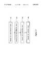
- FIG. 1shows a prior art integrated circuit image sensor array.
- the integrated circuit image sensor arrayincludes a substrate 100.
- An interconnection structure 110is formed adjacent to the substrate 100.
- a pixel interconnect structure 120is formed adjacent to the interconnection structure 110.
- Several layers 130are formed over the pixel interconnect structure 120 which form an array of image sensors.
- electrodes 140, 142, 144form cathodes of the image sensors.
- a transparent conductor 150is formed adjacent to the layers 130 which form the array of image sensors. The transparent conductor 150 provides biasing of the anodes of the image sensors.
- the interconnection structure 110is a standard CMOS interconnection structure.
- the interconnection structureincludes conductive vias 114, 116, 118 which provide electrical connections to the substrate 100.
- the pixel interconnect structure 120provides reliability and structural advantages to the elevated image sensor structure.
- the pixel interconnect structure 120allows for the formation of thin pixel electrodes 140, 142, 144 because the pixel electrodes 140, 142, 144 are formed over silicon rather that a metal pad located on the interconnection structure 110.
- the pixel interconnect structure 120electrically connects the pixel electrodes 140, 142, 144 to the interconnection structure 110.
- the pixel interconnect structure 120is typically formed from a dielectric film, for example, polyimide, silicon oxide or a silicon nitride.
- the pixel interconnect structure 120 of FIG. 1does not provide protection of the conductive vias 114, 116, 118, or electrical circuitry located on the substrate 100 from moisture. Therefore, the conductive vias 114, 116, 118 and the electrical circuitry located on the substrate 100 are susceptible to corrosion.
- the top surface of a passivation layer of a typical integrated circuitis not planar. That is, the top surface is not a well controlled flat surface. Therefore, a typical passivation layer cannot be sandwiched between layers of the integrated circuit image sensor array of FIG. 1.
- a passivation layerHigh temperatures are required to form a passivation layer. Generally, the temperatures required to form the passivation layer are greater than the temperature that most sensors can withstand without being damaged. Therefore, a passivation layer cannot be formed over the integrated circuit image sensor array of FIG. 1. Additionally, a passivation layer formed over an integrated circuit image sensor array could absorb light before the light is absorbed or sensed by the image sensor array.
- a passivation structureformed over a substrate, which includes conductive vias which pass through the passivation structure so that image sensors can be located over the passivation structure and electrically connected to the substrate. It is further desirable that the passivation structure include a planar surface to allow the passivation layer to be sandwiched between the image sensors and the substrate.
- the present inventionis an integrated circuit sensor passivation structure which includes passivation of electrical interconnections and electrical circuitry associated with the image sensor array.
- a first embodiment of the inventionincludes an integrated circuit sensor structure.
- the integrated circuit sensor structureincludes a substrate which includes electronic circuitry.
- An interconnect structureis adjacent to the substrate.
- the interconnect structureincludes conductive interconnect vias which pass through the interconnect structure.
- a dielectric layeris adjacent to the interconnect structure.
- the dielectric layerincludes a planar surface, and conductive dielectric vias which pass through the dielectric layer and are electrically connected to the interconnect vias.
- the dielectric layerfurther includes an interlayer planarization dielectric layer adjacent to the interconnect structure, and a passivating layer adjacent to the interlayer planarization dielectric layer.
- the integrated circuit sensor structurefurther includes sensors adjacent to the dielectric layer. The interconnect vias and the dielectric vias electrically connect the electronic circuitry to the sensors.
- a second embodiment of the inventionis similar to the first embodiment.
- the dielectric layer of the second embodimentfurther includes an adhesion layer adjacent to the passivating layer.
- a third embodiment of the inventionis similar to the first embodiment.
- the sensors of the third embodimentinclude light sensitive active image sensors.
- FIG. 1shows a prior art image sensor array which does not include passivation protection of electrical circuitry associated with the image sensors.
- FIG. 2shows an embodiment of the invention which includes passivation protection of electrical interconnects and electrical circuitry associated with an array of image sensors.
- FIG. 3shows an embodiment of the invention which includes passivation protection of electrical interconnects and electrical circuitry associated with an array of image sensors.
- FIG. 4shows a flow chart which depicts steps of a method of forming the dielectric layer 220 of the embodiments of the invention.
- the inventionis embodied in an image sensor array passivation structure which provides the electrical interconnections and electrical circuitry associated with the image sensor array protection from moisture.
- FIG. 2shows an embodiment of the invention which includes an integrated circuit passivation structure.
- the integrated circuit passivation structureincludes a substrate 200.
- the substrate 200typically includes electronic circuitry.
- An interconnect structure 210is formed adjacent to the substrate 200.
- the interconnect structure 210includes conductive interconnect vias 214, 216, 218 which pass through the interconnect structure 210.
- a dielectric layer 220is formed adjacent to the interconnect structure 210.
- the dielectric layer 220includes a planar surface 228.
- the dielectric layerincludes conductive dielectric vias 222, 224, 226 which pass through the dielectric layer 220 and are electrically connected to the interconnect vias 214, 216, 218.
- the dielectric layer 220further includes an interlayer planarization dielectric layer 230 adjacent to the interconnect structure 210, and a passivating layer 240 adjacent to the dielectric layer 230.
- the passivation structurefurther comprises an array of image sensors 250 adjacent to the dielectric layer 220.
- the interconnect vias 214, 216, 218 and the dielectric vias 222, 224, 226electrically connect the electronic circuitry of the substrate 200 to the image sensors 250.
- a transparent conductor 260generally provides biasing of anodes of the image sensors 250.
- Cathodes of the image sensors 250are generally formed by electrodes 252, 254, 256.
- the electrodes 252, 254, 256are electrically connected to the dielectric vias 222, 224, 226.
- the image sensors 250include electrodes and inner layers. However, the invention is also applicable to other configurations of the image sensors 250. Additionally, the passivation structure of the invention can be used with other elevated devices, such as, organic light emitting diodes.
- the image sensors 250conduct charge when the image sensors receive light.
- the substrate 200generally includes sense circuitry and signal processing circuitry.
- the sense circuitrysenses how much charge the image sensors 250 have conducted.
- the amount of charge conductedrepresents the intensity of light received by the image sensors 250.
- the substrate 200can be CMOS (complementary metal oxide silicon), BiCMOS or Bipolar.
- the substrate 200can include various types of substrate technology including charged coupled devices.
- the interconnect structure 210is a standard interconnection structure.
- the structure and methods of forming the interconnect structure 210are well known in the field of electronic integrated circuit fabrication.
- the interconnect structure 210can be a subtractive metal structure, or a single or dual damascene structure.
- the dielectric layer 220provides reliability and structural advantages to the elevated pixel sensor structure.
- the dielectric layer 220electrically connects the pixel electrodes 252, 254, 256 to the interconnect structure 210.
- the conductive vias 222, 224, 226pass through the dielectric layer 220 and electrically connect the pixel electrodes 252, 254, 256 to the substrate 200.
- the conductive vias 252, 254, 256are formed from tungsten. Tungsten is generally used during fabrication because tungsten can fill high aspect ratio holes. That is, tungsten can be used to form narrow and relatively long interconnections.
- the conductive vias 252, 254, 256are formed using a chemical vapor deposition (CVD) process.
- CVDchemical vapor deposition
- Other materials which can be used to form the conductive vias 252, 254, 256include copper, aluminum or any other electrically conductive material.
- This structureallows the interconnection circuitry to be tightly packed. First of all, lateral space is conserved because the vias 252, 254, 256 are located directly underneath the pixel electrodes. Secondly, the structure allows the formation of vias 252, 254, 256 having a minimal diameter.
- CVD processesare generally the best method of forming the vias 252, 254, 256.
- a Tungsten CVD processallows for the formation of small diameter vias. However, the temperatures required to form tungsten vias with a CVD process are greater than many of the materials (amorphous silicon for example) to form the pixel electrodes can withstand.
- the vias 252, 254, 256can be formed before the pixel electrodes 252, 254, 256, and therefore, the pixel electrodes 252, 254, 256 are not subjected to the high temperatures required for the formation of the vias 252, 254, 256.
- the dielectric layer 220 of FIG. 2includes an interlayer planarization dielectric layer 230 and a passivating layer 240.
- the interlayer planarization dielectric layer 230provides a flat planar surface.
- the interlayer planarization dielectric layer 230includes a low dielectric constant which minimizes interlayer capacitance.
- the planarization of the interlayer planarization dielectric layer 230improves step coverage of the passivating layer 240 which allows the thickness of the passivating layer 240 to be minimized.
- the interlayer planarization dielectric layer 230can be formed from an oxide, like, SiO 2 .
- the passivating layer 240provides protection of the interconnect vias 214, 216, 218 and electronic circuitry on the substrate 200 from moisture.
- the passivating layer 240can be formed from a nitride or a carbide.
- the dielectric layer 220is formed before the image sensors 250. Therefore, the image sensors are not subjected to high temperatures which may be required during the formation of the dielectric layer 220.
- FIG. 3shows another embodiment of the invention.
- This embodimentfurther includes an adhesion layer 310 within the dielectric layer 220 which is formed adjacent to the passivating layer 240.
- the adhesion layer 310provides adhesion between the passivating layer 240 and the image sensors 250.
- the adhesion layer 310can be formed from an oxide, a nitride or a carbide.
- FIG. 4shows a flow chart which depicts steps of a method of forming the dielectric layer 220 of the embodiments of the invention.
- a first step 410 of forming the dielectric layer 220includes depositing the inter-dielectric layer 230 over the interconnect structure 210.
- the inter-dielectric layer 230can be deposited through plasma etch chemical vapor deposition (PECVD).
- PECVDplasma etch chemical vapor deposition
- the inter-dielectric layer 230can also be deposited through bias sputtering which shapes the inter-dielectric layer 230 on the interconnect structure 210. This methods of depositing the dielectric layer 220 are well known in the art of semiconductor processing.
- a second step 420includes planarizing the inter-dielectric layer 230.
- the inter-dielectric layer 230is planarized through a chemical, mechanical process (CMP).
- CMPprovides the best uniformity of the surface.
- CMPis a well known process in the art of semiconductor processing.
- a third step 430includes depositing the passivating layer 240.
- the passivating layer 240is typically deposited through bias sputtering process or a sputter deposit process. These depositing processes are well known in the art of semiconductor processing.
- a fourth step 440includes depositing the adhesion layer 310.
- the adhesion layer 310is typically deposited through bias sputtering process or a sputter deposit process. These depositing processes are well known in the art of semiconductor processing.
- Viasare etched through the dielectric layer 220 to allow for the deposition of the pixel electrodes 252, 254, 256.
Landscapes
- Internal Circuitry In Semiconductor Integrated Circuit Devices (AREA)
- Solid State Image Pick-Up Elements (AREA)
- Formation Of Insulating Films (AREA)
- Production Of Multi-Layered Print Wiring Board (AREA)
Abstract
Description
Claims (9)
Priority Applications (3)
| Application Number | Priority Date | Filing Date | Title |
|---|---|---|---|
| US09/306,238US6051867A (en) | 1999-05-06 | 1999-05-06 | Interlayer dielectric for passivation of an elevated integrated circuit sensor structure |
| JP2000127497AJP4501123B2 (en) | 1999-05-06 | 2000-04-27 | Improved interlayer dielectric for passivation of elevated integrated circuit sensor structures |
| EP00303822AEP1052698A3 (en) | 1999-05-06 | 2000-05-08 | Interlayer dielectric for integrated circuit |
Applications Claiming Priority (1)
| Application Number | Priority Date | Filing Date | Title |
|---|---|---|---|
| US09/306,238US6051867A (en) | 1999-05-06 | 1999-05-06 | Interlayer dielectric for passivation of an elevated integrated circuit sensor structure |
Publications (1)
| Publication Number | Publication Date |
|---|---|
| US6051867Atrue US6051867A (en) | 2000-04-18 |
Family
ID=23184429
Family Applications (1)
| Application Number | Title | Priority Date | Filing Date |
|---|---|---|---|
| US09/306,238Expired - LifetimeUS6051867A (en) | 1999-05-06 | 1999-05-06 | Interlayer dielectric for passivation of an elevated integrated circuit sensor structure |
Country Status (3)
| Country | Link |
|---|---|
| US (1) | US6051867A (en) |
| EP (1) | EP1052698A3 (en) |
| JP (1) | JP4501123B2 (en) |
Cited By (13)
| Publication number | Priority date | Publication date | Assignee | Title |
|---|---|---|---|---|
| US6229191B1 (en)* | 1999-11-19 | 2001-05-08 | Agilent Technologies, Inc. | Conductive guard rings for elevated active pixel sensors |
| US6384460B1 (en)* | 1999-06-07 | 2002-05-07 | Agilent Technologies, Inc. | Self-aligned metal electrode structure for elevated sensors |
| US6392301B1 (en)* | 1999-10-22 | 2002-05-21 | Intel Corporation | Chip package and method |
| US20030085410A1 (en)* | 2001-03-16 | 2003-05-08 | Theil Jeremy A. | Simplified upper electrode contact structure for PIN diode active pixel sensor |
| FR2844098A1 (en)* | 2002-09-03 | 2004-03-05 | Atmel Grenoble Sa | OPTICAL MICROSYSTEM AND MANUFACTURING METHOD |
| WO2004097930A1 (en)* | 2003-04-28 | 2004-11-11 | Fujitsu Limited | Semiconductor device and method for fabricating the same |
| US20040238911A1 (en)* | 2003-05-26 | 2004-12-02 | Francois Roy | Photodetector array |
| US20050042794A1 (en)* | 2000-12-21 | 2005-02-24 | Stmicroelectronic N.V. | Optoelectronic component for converting electromagnetic radiation into an intensity-dependent photocurrent |
| US20070085120A1 (en)* | 2005-10-15 | 2007-04-19 | Chartered Semiconductor Manufacturing Ltd. | Optical color sensor system |
| US20080224137A1 (en)* | 2007-03-14 | 2008-09-18 | Jin Ha Park | Image Sensor and Method for Manufacturing the Same |
| US20090189233A1 (en)* | 2008-01-25 | 2009-07-30 | Taiwan Semiconductor Manufacturing Co., Ltd. | Cmos image sensor and method for manufacturing same |
| CN101640213A (en)* | 2008-07-29 | 2010-02-03 | 东部高科股份有限公司 | Image sensor and fabrication method thereof |
| US20110140222A1 (en)* | 2003-04-02 | 2011-06-16 | Round Rock Research, Llc | Passivation planarization |
Families Citing this family (1)
| Publication number | Priority date | Publication date | Assignee | Title |
|---|---|---|---|---|
| JP6711573B2 (en)* | 2015-08-10 | 2020-06-17 | ソニーセミコンダクタソリューションズ株式会社 | Solid-state image sensor |
Citations (4)
| Publication number | Priority date | Publication date | Assignee | Title |
|---|---|---|---|---|
| US4571626A (en)* | 1981-09-17 | 1986-02-18 | Matsushita Electric Industrial Co., Ltd. | Solid state area imaging apparatus |
| US4739384A (en)* | 1984-10-22 | 1988-04-19 | Fuji Photo Film Co., Ltd. | Solid-state imaging device with polycrystalline film |
| US5929474A (en)* | 1997-03-10 | 1999-07-27 | Motorola, Inc. | Active matrix OED array |
| US5936261A (en)* | 1998-11-18 | 1999-08-10 | Hewlett-Packard Company | Elevated image sensor array which includes isolation between the image sensors and a unique interconnection |
Family Cites Families (7)
| Publication number | Priority date | Publication date | Assignee | Title |
|---|---|---|---|---|
| CA2034118A1 (en)* | 1990-02-09 | 1991-08-10 | Nang Tri Tran | Solid state radiation detector |
| US5273910A (en)* | 1990-08-08 | 1993-12-28 | Minnesota Mining And Manufacturing Company | Method of making a solid state electromagnetic radiation detector |
| US5182624A (en)* | 1990-08-08 | 1993-01-26 | Minnesota Mining And Manufacturing Company | Solid state electromagnetic radiation detector fet array |
| JPH05152554A (en)* | 1991-09-30 | 1993-06-18 | Toshiba Corp | Solid-state imaging device |
| EP0688672B1 (en)* | 1994-06-24 | 1999-06-16 | Hewlett-Packard Company | Ink jet printhead having a palladium cavitation barrier and interconnect layer |
| JP3183390B2 (en)* | 1995-09-05 | 2001-07-09 | キヤノン株式会社 | Photoelectric conversion device and imaging device using the same |
| JP3447947B2 (en)* | 1998-03-20 | 2003-09-16 | 株式会社東芝 | X-ray imaging device |
- 1999
- 1999-05-06USUS09/306,238patent/US6051867A/ennot_activeExpired - Lifetime
- 2000
- 2000-04-27JPJP2000127497Apatent/JP4501123B2/ennot_activeExpired - Lifetime
- 2000-05-08EPEP00303822Apatent/EP1052698A3/ennot_activeCeased
Patent Citations (4)
| Publication number | Priority date | Publication date | Assignee | Title |
|---|---|---|---|---|
| US4571626A (en)* | 1981-09-17 | 1986-02-18 | Matsushita Electric Industrial Co., Ltd. | Solid state area imaging apparatus |
| US4739384A (en)* | 1984-10-22 | 1988-04-19 | Fuji Photo Film Co., Ltd. | Solid-state imaging device with polycrystalline film |
| US5929474A (en)* | 1997-03-10 | 1999-07-27 | Motorola, Inc. | Active matrix OED array |
| US5936261A (en)* | 1998-11-18 | 1999-08-10 | Hewlett-Packard Company | Elevated image sensor array which includes isolation between the image sensors and a unique interconnection |
Cited By (28)
| Publication number | Priority date | Publication date | Assignee | Title |
|---|---|---|---|---|
| US6384460B1 (en)* | 1999-06-07 | 2002-05-07 | Agilent Technologies, Inc. | Self-aligned metal electrode structure for elevated sensors |
| US6392301B1 (en)* | 1999-10-22 | 2002-05-21 | Intel Corporation | Chip package and method |
| US6229191B1 (en)* | 1999-11-19 | 2001-05-08 | Agilent Technologies, Inc. | Conductive guard rings for elevated active pixel sensors |
| US20060223214A1 (en)* | 2000-12-20 | 2006-10-05 | Stmicroelectronics N.V. | Optoelectronic component for converting electromagnetic radiation into a intensity-dependent photocurrent |
| US20050042794A1 (en)* | 2000-12-21 | 2005-02-24 | Stmicroelectronic N.V. | Optoelectronic component for converting electromagnetic radiation into an intensity-dependent photocurrent |
| US20030085410A1 (en)* | 2001-03-16 | 2003-05-08 | Theil Jeremy A. | Simplified upper electrode contact structure for PIN diode active pixel sensor |
| US6649993B2 (en) | 2001-03-16 | 2003-11-18 | Agilent Technologies, Inc. | Simplified upper electrode contact structure for PIN diode active pixel sensor |
| US6902946B2 (en) | 2001-03-16 | 2005-06-07 | Agilent Technologies, Inc. | Simplified upper electrode contact structure for PIN diode active pixel sensor |
| WO2004023166A3 (en)* | 2002-09-03 | 2004-05-13 | Atmel Grenoble Sa | Optical microsystem and method for making same |
| US7737518B2 (en) | 2002-09-03 | 2010-06-15 | Atmel Grenoble S.A. | Optical microsystem and fabrication process |
| FR2844098A1 (en)* | 2002-09-03 | 2004-03-05 | Atmel Grenoble Sa | OPTICAL MICROSYSTEM AND MANUFACTURING METHOD |
| US7407825B2 (en) | 2002-09-03 | 2008-08-05 | E2V Semiconductors | Optical microsystem and method for making same |
| US20080151131A1 (en)* | 2002-09-03 | 2008-06-26 | Philippe Rommeveaux | Optical microsystem and fabrication process |
| US20110140222A1 (en)* | 2003-04-02 | 2011-06-16 | Round Rock Research, Llc | Passivation planarization |
| US7492047B2 (en)* | 2003-04-28 | 2009-02-17 | Fujitsu Limited | Semiconductor device and its manufacture method |
| US20050242402A1 (en)* | 2003-04-28 | 2005-11-03 | Narumi Ohkawa | Semiconductor device and its manufacture method |
| WO2004097930A1 (en)* | 2003-04-28 | 2004-11-11 | Fujitsu Limited | Semiconductor device and method for fabricating the same |
| US20040238911A1 (en)* | 2003-05-26 | 2004-12-02 | Francois Roy | Photodetector array |
| US7279729B2 (en) | 2003-05-26 | 2007-10-09 | Stmicroelectronics S.A. | Photodetector array |
| EP1482558A3 (en)* | 2003-05-26 | 2005-02-23 | STMicroelectronics S.A. | Photo detector array |
| US20070085120A1 (en)* | 2005-10-15 | 2007-04-19 | Chartered Semiconductor Manufacturing Ltd. | Optical color sensor system |
| US7446386B2 (en) | 2005-10-15 | 2008-11-04 | Chartered Semiconductor Manufacturing Ltd. | Optical color sensor system |
| US20090026568A1 (en)* | 2005-10-15 | 2009-01-29 | Chartered Semiconductor Manufacturing Ltd. | Optical color sensor system |
| US8188560B2 (en) | 2005-10-15 | 2012-05-29 | Globalfoundries Singapore Pte. Ltd. | Optical color sensor system |
| US20080224137A1 (en)* | 2007-03-14 | 2008-09-18 | Jin Ha Park | Image Sensor and Method for Manufacturing the Same |
| US7732813B2 (en)* | 2007-03-14 | 2010-06-08 | Dongbu Hitek Co., Ltd. | Image sensor and method for manufacturing the same |
| US20090189233A1 (en)* | 2008-01-25 | 2009-07-30 | Taiwan Semiconductor Manufacturing Co., Ltd. | Cmos image sensor and method for manufacturing same |
| CN101640213A (en)* | 2008-07-29 | 2010-02-03 | 东部高科股份有限公司 | Image sensor and fabrication method thereof |
Also Published As
| Publication number | Publication date |
|---|---|
| JP4501123B2 (en) | 2010-07-14 |
| JP2001024059A (en) | 2001-01-26 |
| EP1052698A3 (en) | 2001-08-29 |
| EP1052698A2 (en) | 2000-11-15 |
Similar Documents
| Publication | Publication Date | Title |
|---|---|---|
| US5936261A (en) | Elevated image sensor array which includes isolation between the image sensors and a unique interconnection | |
| US6018187A (en) | Elevated pin diode active pixel sensor including a unique interconnection structure | |
| US6051867A (en) | Interlayer dielectric for passivation of an elevated integrated circuit sensor structure | |
| US6016000A (en) | Ultra high-speed chip semiconductor integrated circuit interconnect structure and fabrication method using free-space dielectrics | |
| US8211740B2 (en) | Solid state imaging device having wirings with diffusion prevention film | |
| US6159851A (en) | Borderless vias with CVD barrier layer | |
| US5300456A (en) | Metal-to-metal antifuse structure | |
| US7332428B2 (en) | Metal interconnect structure and method | |
| US6143672A (en) | Method of reducing metal voidings in 0.25 μm AL interconnect | |
| US6265319B1 (en) | Dual damascene method employing spin-on polymer (SOP) etch stop layer | |
| KR20010020476A (en) | Ultra high-speed chip interconnect using free-space dielectrics | |
| US6215164B1 (en) | Elevated image sensor array which includes isolation between uniquely shaped image sensors | |
| US20030234416A1 (en) | Capacitor for a semiconductor device and method for fabrication therefor | |
| US6174797B1 (en) | Silicon oxide dielectric material with excess silicon as diffusion barrier layer | |
| US20020155676A1 (en) | Zero mask MIMcap process for a low k BEOL | |
| US7329585B2 (en) | Method of manufacturing semiconductor device | |
| US20210384093A1 (en) | Integrated circuit device | |
| US6440838B1 (en) | Dual damascene structure employing laminated intermediate etch stop layer | |
| KR20010024096A (en) | Method and apparatus for high-performance integrated circuit interconnect fabrication | |
| US20040251552A1 (en) | Semiconductor device and manufacturing method the same | |
| US6974770B2 (en) | Self-aligned mask to reduce cell layout area | |
| US6180507B1 (en) | Method of forming interconnections | |
| US7256118B2 (en) | Semiconductor device using low-K material as interlayer insulating film and its manufacture method | |
| US8796804B2 (en) | Forming sensing elements above a semiconductor substrate | |
| US20030116826A1 (en) | Interconnect structure capped with a metallic barrier layer and method fabrication thereof |
Legal Events
| Date | Code | Title | Description |
|---|---|---|---|
| AS | Assignment | Owner name:HEWLETT-PACKARD COMPANY, CALIFORNIA Free format text:ASSIGNMENT OF ASSIGNORS INTEREST;ASSIGNORS:THEIL, JEREMY A.;RAY, GARY W.;PERNER, FREDERICK A.;AND OTHERS;REEL/FRAME:010087/0504;SIGNING DATES FROM 19990430 TO 19990506 | |
| STCF | Information on status: patent grant | Free format text:PATENTED CASE | |
| AS | Assignment | Owner name:HEWLETT-PACKARD COMPANY, COLORADO Free format text:MERGER;ASSIGNOR:HEWLETT-PACKARD COMPANY;REEL/FRAME:010759/0049 Effective date:19980520 | |
| AS | Assignment | Owner name:AGILENT TECHNOLOGIES INC, CALIFORNIA Free format text:ASSIGNMENT OF ASSIGNORS INTEREST;ASSIGNOR:HEWLETT-PACKARD COMPANY;REEL/FRAME:010977/0540 Effective date:19991101 | |
| FEPP | Fee payment procedure | Free format text:PAYOR NUMBER ASSIGNED (ORIGINAL EVENT CODE: ASPN); ENTITY STATUS OF PATENT OWNER: LARGE ENTITY | |
| FPAY | Fee payment | Year of fee payment:4 | |
| AS | Assignment | Owner name:AVAGO TECHNOLOGIES GENERAL IP PTE. LTD., SINGAPORE Free format text:ASSIGNMENT OF ASSIGNORS INTEREST;ASSIGNOR:AGILENT TECHNOLOGIES, INC.;REEL/FRAME:017207/0020 Effective date:20051201 | |
| AS | Assignment | Owner name:AVAGO TECHNOLOGIES SENSOR IP PTE. LTD., SINGAPORE Free format text:ASSIGNMENT OF ASSIGNORS INTEREST;ASSIGNOR:AVAGO TECHNOLOGIES GENERAL IP (SINGAPORE) PTE. LTD.;REEL/FRAME:018545/0426 Effective date:20061024 | |
| AS | Assignment | Owner name:MICRON TECHNOLOGY, INC.,IDAHO Free format text:ASSIGNMENT OF ASSIGNORS INTEREST;ASSIGNOR:AVAGO TECHNOLOGIES IMAGING HOLDING CORPORATION;REEL/FRAME:018757/0159 Effective date:20061206 Owner name:MICRON TECHNOLOGY, INC., IDAHO Free format text:ASSIGNMENT OF ASSIGNORS INTEREST;ASSIGNOR:AVAGO TECHNOLOGIES IMAGING HOLDING CORPORATION;REEL/FRAME:018757/0159 Effective date:20061206 | |
| AS | Assignment | Owner name:MICRON TECHNOLOGY, INC.,IDAHO Free format text:ASSIGNMENT OF ASSIGNORS INTEREST;ASSIGNOR:AVAGO TECHNOLOGIES IMAGING HOLDING CORPORATION;REEL/FRAME:019407/0441 Effective date:20061206 Owner name:MICRON TECHNOLOGY, INC., IDAHO Free format text:ASSIGNMENT OF ASSIGNORS INTEREST;ASSIGNOR:AVAGO TECHNOLOGIES IMAGING HOLDING CORPORATION;REEL/FRAME:019407/0441 Effective date:20061206 | |
| XAS | Not any more in us assignment database | Free format text:CORRECTED COVER SHEET TO ADD PORTION OF THE PAGE THAT WAS PREVIOUSLY OMITTED FROM THE NOTICE AT REEL/FRAME 018757/0183 (ASSIGNMENT OF ASSIGNOR'S INTEREST);ASSIGNOR:AVAGO TECHNOLOGIES IMAGING HOLDING CORPORATION;REEL/FRAME:019028/0237 | |
| FPAY | Fee payment | Year of fee payment:8 | |
| AS | Assignment | Owner name:AVAGO TECHNOLOGIES IMAGING HOLDING CORPORATION, MA Free format text:ASSIGNMENT OF ASSIGNORS INTEREST;ASSIGNOR:AVAGO TECHNOLOGIES SENSOR IP PTE. LTD.;REEL/FRAME:021603/0690 Effective date:20061122 Owner name:AVAGO TECHNOLOGIES IMAGING HOLDING CORPORATION,MAL Free format text:ASSIGNMENT OF ASSIGNORS INTEREST;ASSIGNOR:AVAGO TECHNOLOGIES SENSOR IP PTE. LTD.;REEL/FRAME:021603/0690 Effective date:20061122 | |
| AS | Assignment | Owner name:APTINA IMAGING CORPORATION,CAYMAN ISLANDS Free format text:ASSIGNMENT OF ASSIGNORS INTEREST;ASSIGNOR:MICRON TECHNOLOGY, INC.;REEL/FRAME:024160/0051 Effective date:20081003 | |
| FPAY | Fee payment | Year of fee payment:12 | |
| AS | Assignment | Owner name:AVAGO TECHNOLOGIES GENERAL IP (SINGAPORE) PTE. LTD Free format text:CORRECTIVE ASSIGNMENT TO CORRECT THE NAME OF THE ASSIGNEE PREVIOUSLY RECORDED ON REEL 017207 FRAME 0020. ASSIGNOR(S) HEREBY CONFIRMS THE ASSIGNMENT;ASSIGNOR:AGILENT TECHNOLOGIES, INC.;REEL/FRAME:038633/0001 Effective date:20051201 |