US6049496A - Circuit and method for low voltage, current sense amplifier - Google Patents
Circuit and method for low voltage, current sense amplifierDownload PDFInfo
- Publication number
- US6049496A US6049496AUS09/050,443US5044398AUS6049496AUS 6049496 AUS6049496 AUS 6049496AUS 5044398 AUS5044398 AUS 5044398AUS 6049496 AUS6049496 AUS 6049496A
- Authority
- US
- United States
- Prior art keywords
- body region
- transistor
- forming
- sense amplifier
- pair
- Prior art date
- Legal status (The legal status is an assumption and is not a legal conclusion. Google has not performed a legal analysis and makes no representation as to the accuracy of the status listed.)
- Expired - Lifetime
Links
- 238000000034methodMethods0.000titleclaimsabstractdescription50
- 239000004065semiconductorSubstances0.000claimsabstractdescription57
- 229910044991metal oxideInorganic materials0.000claimsabstractdescription19
- 150000004706metal oxidesChemical class0.000claimsabstractdescription19
- 210000000746body regionAnatomy0.000claimsdescription41
- 239000000463materialSubstances0.000claimsdescription40
- 239000000758substrateSubstances0.000claimsdescription27
- 229910021420polycrystalline siliconInorganic materials0.000claimsdescription23
- 229920005591polysiliconPolymers0.000claimsdescription22
- 230000000295complement effectEffects0.000claimsdescription17
- 239000012212insulatorSubstances0.000claimsdescription12
- 238000004519manufacturing processMethods0.000claimsdescription10
- 230000008878couplingEffects0.000claimsdescription4
- 238000010168coupling processMethods0.000claimsdescription4
- 238000005859coupling reactionMethods0.000claimsdescription4
- 230000008901benefitEffects0.000abstractdescription7
- 230000004044responseEffects0.000abstractdescription3
- 229920002120photoresistant polymerPolymers0.000description19
- 238000005229chemical vapour depositionMethods0.000description13
- 238000001020plasma etchingMethods0.000description12
- 150000004767nitridesChemical class0.000description9
- 238000005530etchingMethods0.000description8
- 239000002210silicon-based materialSubstances0.000description8
- 238000005516engineering processMethods0.000description7
- 229910052751metalInorganic materials0.000description7
- 239000002184metalSubstances0.000description7
- 230000008569processEffects0.000description7
- 235000012431wafersNutrition0.000description7
- XUIMIQQOPSSXEZ-UHFFFAOYSA-NSiliconChemical compound[Si]XUIMIQQOPSSXEZ-UHFFFAOYSA-N0.000description5
- 230000009471actionEffects0.000description5
- 238000010586diagramMethods0.000description5
- 239000003870refractory metalSubstances0.000description5
- VYPSYNLAJGMNEJ-UHFFFAOYSA-NSilicium dioxideChemical compoundO=[Si]=OVYPSYNLAJGMNEJ-UHFFFAOYSA-N0.000description4
- 229910052710siliconInorganic materials0.000description4
- 239000010703siliconSubstances0.000description4
- 229910052785arsenicInorganic materials0.000description3
- RQNWIZPPADIBDY-UHFFFAOYSA-Narsenic atomChemical group[As]RQNWIZPPADIBDY-UHFFFAOYSA-N0.000description3
- 238000005468ion implantationMethods0.000description3
- ZOXJGFHDIHLPTG-UHFFFAOYSA-NBoronChemical compound[B]ZOXJGFHDIHLPTG-UHFFFAOYSA-N0.000description2
- NBIIXXVUZAFLBC-UHFFFAOYSA-NPhosphoric acidChemical compoundOP(O)(O)=ONBIIXXVUZAFLBC-UHFFFAOYSA-N0.000description2
- 229910052796boronInorganic materials0.000description2
- 239000004020conductorSubstances0.000description2
- 229910021419crystalline siliconInorganic materials0.000description2
- 239000002019doping agentSubstances0.000description2
- 150000002500ionsChemical class0.000description2
- 239000000377silicon dioxideSubstances0.000description2
- 235000012239silicon dioxideNutrition0.000description2
- 230000003213activating effectEffects0.000description1
- 230000004913activationEffects0.000description1
- 230000006978adaptationEffects0.000description1
- 229910000147aluminium phosphateInorganic materials0.000description1
- 238000000137annealingMethods0.000description1
- 238000003491arrayMethods0.000description1
- 230000015572biosynthetic processEffects0.000description1
- 230000008859changeEffects0.000description1
- 230000005669field effectEffects0.000description1
- 230000006870functionEffects0.000description1
- 239000012535impuritySubstances0.000description1
- 238000001465metallisationMethods0.000description1
- 229910021421monocrystalline siliconInorganic materials0.000description1
- 238000005498polishingMethods0.000description1
- 125000006850spacer groupChemical group0.000description1
- 239000000126substanceSubstances0.000description1
- WFKWXMTUELFFGS-UHFFFAOYSA-NtungstenChemical compound[W]WFKWXMTUELFFGS-UHFFFAOYSA-N0.000description1
- 229910052721tungstenInorganic materials0.000description1
- 239000010937tungstenSubstances0.000description1
Images


Classifications
- G—PHYSICS
- G11—INFORMATION STORAGE
- G11C—STATIC STORES
- G11C7/00—Arrangements for writing information into, or reading information out from, a digital store
- G11C7/06—Sense amplifiers; Associated circuits, e.g. timing or triggering circuits
- G11C7/062—Differential amplifiers of non-latching type, e.g. comparators, long-tailed pairs
- G—PHYSICS
- G11—INFORMATION STORAGE
- G11C—STATIC STORES
- G11C7/00—Arrangements for writing information into, or reading information out from, a digital store
- G11C7/06—Sense amplifiers; Associated circuits, e.g. timing or triggering circuits
- G11C7/065—Differential amplifiers of latching type
Definitions
- the present inventionrelates generally to semiconductor integrated circuits. More particularly, it pertains to circuits, methods and structure for gated lateral bipolar transistors.
- Integrated circuit technologyrelies on transistors to formulate vast arrays of functional circuits.
- the complexity of these circuitsrequire the use of an ever increasing number of linked transistors.
- the surface space on silicon chip/diedwindles. It is one objective then, to construct transistors which occupy less surface area on the silicon chip/die.
- MOS transistorsMetal-oxide semiconductor field effect transistors
- Bipolar transistorson the other hand, also possess certain advantages over MOS transistors, such as speed. Therefore, it is another objective and attempts have been made to combine the technological designs of bipolars and MOS transistors in an effort to maximize the benefits of both transistor types.
- CMOScomplementary metal-oxide semiconductor
- BiCMOSbipolar complementary metal-oxide semiconductor
- gate-body connected MOS transistorsand gated lateral bipolar transistors have been described.
- the term gate-body connected transistorsis used to describe vertical or other device structures where the body of the MOS transistor also serves as the base of a bipolar transistor but each device functions separately as a normal transistor and MOS transistor action is dominant. Applying the gate voltage to the body serves primarily to change the threshold voltage of the MOS transistor.
- gate and baseare common and the bipolar transistor and MOS transistor are in parallel but the bipolar transistor current is dominant.
- a gated lateral transistornot only the structures but also the operation is merged and most current flows along a surface under the gate in either MOS or bipolar operation.
- a gated lateral bipolar transistorat low gate voltages around threshold (V t ), they can act as gate-body connected MOS transistors. At higher input voltages, V t or more, the bipolar action can dominate and they are more appropriately described as gated lateral bipolar transistors.
- an illustrative embodiment of the present inventionincludes a current sense amplifier.
- the current sense amplifierincludes a pair of cross coupled inverters where each inverter is formed from a complementary pair of gated lateral bipolar transistors.
- the complementary pairincludes both a first channel type transistor and a second channel type transistor.
- the gated lateral bipolar transistorincludes a first layer of semiconductor material extending outwardly from a substrate.
- the first layer of semiconductor materialhas opposing sidewall surfaces and an upper surface.
- the gated lateral bipolar transistorhas a second layer of semiconductor material formed on and extending outwardly from the upper surface of the first layer of semiconductor material.
- the second layer of semiconductor materialsimilarly has opposing sidewall surfaces and an upper surface.
- the gated lateral bipolar transistorincludes a emitter/source region and a collector/drain region formed on portions of the upper surface of the second layer.
- the gated lateral bipolar transistorincludes a dielectric layer formed on a portion of the upper surface of the second layer of semiconductor material and on portions of the opposing sidewall surfaces of the first and second layers of semiconductor material. There is a gate formed on the dielectric layer.
- Conductive sidewall membersare disposed adjacent to portions of the dielectric layer which are formed on the opposing sidewall surfaces of the first and second layers of semiconductor material. The conductive sidewall members couple to the gate, and to portions of the first layer of semiconductor material such that the transistors give metal-oxide semiconductor (MOS) type conduction and bipolar junction transistor (BJT) type conduction underneath the gate.
- MOSmetal-oxide semiconductor
- BJTbipolar junction transistor
- the current sense amplifieralso includes a pair of bit lines coupled to the inputs of the first channel type transistor in each inverter. Further the current sense amplifier includes a pair of input/output lines where each one of the pair of input/output lines couples to an output of one of the cross-coupled inverters and to the gates of the other inverter.
- a current sense amplifier circuitin another embodiment, includes a pair of cross coupled inverters, wherein each inverter comprises a complementary pair of gated lateral bipolar transistors.
- the complementary paircomprises a first channel type transistor and a second channel type transistor.
- Each gated lateral bipolar transistorhas a body region formed of single crystalline semiconductor material which extends outwardly from a substrate.
- the body regionhas an upper surface and opposing sidewalls.
- the body regionadditionally has a highly doped, retrograded bottom layer.
- a emitter/source region and a collector/drain regionis formed within a portion of the upper surface of the body region.
- a gateis formed above the upper surface of the body region.
- Conductive sidewall membersare disposed adjacent to the opposing sidewalls of the body region.
- a pair of bit linescouple to the inputs of the first channel type transistors in each inverter.
- a pair of input/output lineseach individually couple to an output of one of the cross-coupled inverters and to the gates of the other inverter.
- a method of fabricating a current sense amplifierincludes forming a pair of cross coupled inverters where each inverter comprises a pair of gated lateral bipolar transistors.
- Forming the gated lateral bipolar transistorsincludes forming a first layer of semiconductor material which extends outwardly from a substrate.
- the first layer of semiconductor materialis formed to have opposing sidewall surfaces and an upper surface.
- the methodfurther includes forming a second layer of semiconductor material on and extending outwardly from the upper surface of the first layer of semiconductor material.
- the second layer of semiconductor materialis also formed having opposing sidewall surfaces and an upper surface. A emitter/source region and a collector/drain region are formed on a portion of the upper surface of the second layer.
- the methodincludes forming a dielectric layer on a portion of the upper surface of the second layer of semiconductor material and on portions of the opposing sidewall surfaces of the first and second layer of semiconductor material.
- a gateis formed on the dielectric layer.
- the methodadditionally includes forming conductive sidewall members disposed adjacent to portions of the dielectric layer and formed on the opposing sidewall surfaces of the first and second layer of semiconductor materials.
- the conductive sidewall membersare formed to couple to the gate and to portions of the first layer of semiconductor material such that the transistors give metal-oxide semiconductor (MOS) type conduction and bipolar junction transistor (BJT) type conduction underneath the gate.
- a pair of bit linesare formed to couple to the inputs of the first channel type transistors in each inverter.
- a pair of input/output linesare forming such that each one individually couples to an output of one of the cross-coupled inverters and to the gates of the other inverter.
- an information handling systemin another embodiment, includes a central processing unit, a random access memory, and a system bus for communicatively coupling the central processing unit and the random access memory.
- the information handling systemfurther includes a current sense amplifier.
- the current sense amplifierincludes the embodiment presented above.
- the circuitincludes transistors which combine BJT and MOS transistor conduction.
- This new circuitallows for low voltage level operation and enhanced switching action over conventional bipolar complementary metal-oxide semiconductor (BiCMOS) devices.
- BiCMOSbipolar complementary metal-oxide semiconductor
- the improved circuitemploys gated lateral bipolar connected transistors in a format which is fully compatible with CMOS technology. Thus, the circuit does not require additional chip surface space, nor additional processing steps.
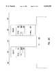
- FIG. 1Ais a perspective view illustrating a current sense amplifier according to the teachings of the present invention.
- FIG. 1Bis a top view of the current sense amplifier shown in FIG. 1A.
- FIG. 1Cis a schematic diagram illustrating an embodiment of the current sense amplifier of FIG. 1A.
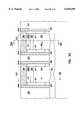
- FIGS. 2A-2Jillustrate an embodiment of a process of fabrication of a current sense amplifier.
- FIG. 3is a block diagram illustrating an information handling system according to an embodiment of the present invention.
- wafer and substrate used in the following descriptioninclude any structure having an exposed surface with which to form the integrated circuit (IC) structure of the invention.
- substrateis understood to include semiconductor wafers.
- substrateis also used to refer to semiconductor structures during processing, and may include other layers that have been fabricated thereupon. Both wafer and substrate include doped and undoped semiconductors, epitaxial semiconductor layers supported by a base semiconductor or insulator, as well as other semiconductor structures well known to one skilled in the art.
- conductoris understood to include semiconductors
- insulatoris defined to include any material that is less electrically conductive than the materials referred to as conductors.
- horizontalas used in this application is defined as a plane parallel to the conventional plane or surface of a wafer or substrate, regardless of the orientation of the wafer or substrate.
- verticalrefers to a direction perpendicular to the horizonal as defined above. Prepositions, such as “on”, “side” (as in “sidewall”), “higher”, “lower”, “over” and “under” are defined with respect to the conventional plane or surface being on the top surface of the wafer or substrate, regardless of the orientation of the wafer or substrate.
- n+refers to semiconductor material that is heavily doped n-type semiconductor material, e.g., monocrystalline silicon or polycrystalline silicon.
- p+refers to semiconductor material that is heavily doped p-type semiconductor material.
- n- and p-refer to lightly doped n and p-type semiconductor materials, respectively.
- FIG. 1Ais a perspective view illustrating generally an embodiment of a portion of a current sense amplifier according to the teachings of the present invention.
- current sense amplifier 50is a six transistor device. Four of of the six transistors are formed using, for example, the technique described below with respect to FIGS. 2A through 2J. It is these four transistors which are the focus of the present invention.
- Each of these four transistors in current sense amplifier 50is either an n-channel metal-oxide semiconductor (NMOS) or a p-channel metal-oxide semiconductor (PMOS) transistor. Two of the four transistors arc NMOS transistors, Q 2 and Q 4 respectively. The other two arm PMOS transistors, Q 1 and Q 3 respectively.
- NMOSn-channel metal-oxide semiconductor
- PMOSp-channel metal-oxide semiconductor
- Each NMOS and PMOS transistorincludes a body region, 110 and 105 respectively, formed of single crystalline semiconductor material that extends outwardly from a substrate 100.
- the body regions 110 and 105have an upper surface 112 and opposing sidewalls 111.
- the NMOS body region 110is formed from a p- silicon material and the PMOS body region 105 is formed from n- silicon material.
- the substrate 100is p- silicon material.
- the NMOS and PMOS body regions, 110 and 105 respectivelyare formed on an insulator layer 180 formed on the substrate 100.
- Both of the NMOS and PMOS transistorsinclude emitter/source regions, 106 and 108 respectively, formed within the upper surface 112 of the body regions, 110 and 105 respectively.
- each of the NMOS and PMOS transistorsinclude a collector/drain region, 107 and 109 respectively, formed within the upper surface 112 of the body regions, 110 and 105 respectively.
- a dielectric layer 120is formed on the upper surface 112 and on portions of the opposing sidewalls 111 for both the NMOS and PMOS transistors.
- the NMOS transistors, Q 2 and Q 4include a gate 130 on the dielectric layer 120.
- the PMOS transistors, Q 1 and Q 3include a gate 131 formed on the dielectric layer 120.
- gate 131is formed of p+ silicon material and gate 130 is formed of n+ silicon material.
- the NMOS transistors, Q 2 and Q 4include conductive sidewall members 140.
- the PMOS transistors, Q 1 and Q 3similarly include conductive sidewall members 145.
- the conductive sidewall members 140are formed of p+ silicon material and the conductive sidewall members 145 are formed of n+ silicon material.
- Conductive sidewall members, 140 and 145 respectively,are disposed adjacent to portions of the dielectric layer 120 formed on the opposing sidewall surfaces 111.
- the conductive sidewall members, 140 and 145respectively, couple to the gates, 130 and 131 respectively, of the NMOS and PMOS transistors.
- the conductive sidewall members, 140 and 145 respectivelyfurther couple to a portion of the opposing sidewalls 111 of the NMOS and PMOS transistors such that the transistors give metal oxide semiconductor (MOS) type conduction and bipolar junction transistor (BJT) type conduction underneath the gates, 130 and 131 respectively.
- MOSmetal oxide semiconductor
- BJTbipolar junction transistor
- the conductive sidewall members, 140 and 145 respectivelyare formed of polysilicon.
- Current sense amplifier 50also includes cross-coupled inverters 104 and 103.
- Inverter 103comprises the combination of transistor Q 1 and Q 2 .
- the gates of transistors Q 1 and Q 2are coupled together by gate contact 160.
- Gate contact 160couples to gate 130 of transistor Q 2 through a refractory metal 132.
- Gate contact 160couples to gate 131 of transistor Q 1 through a refractory metal 132.
- inverter 104includes transistors Q 3 and Q 4 .
- the gates of transistors Q 3 and Q 4are coupled together by gate contact 161.
- Gate contact 161couples to gate 130 of transistor Q 4 through a refractory metal 132.
- gate contact 161couples to gate 131 of transistor Q 3 through a refractory metal 132.
- the collector/drain regions, 107 and 109 respectively, of inverter 103are coupled together by a metal shunt 162.
- the collector/drain regions, 107 and 109 respectively, of inverter 104are coupled together by a shunt 163.
- Metal shunt 163is cross-coupled to gate contact 160.
- Metal shunt 162is cross-coupled to gate contact 161.
- a pair of bit lines (BL and BL*), 190 and 192 respectively,are coupled to the emitter/source regions 106 of transistors Q 2 and Q 4 .
- the emitter/source regions 106 of transistors Q 2 and Q 4are additionally coupled to ground through gated lateral NMOS transistors, shown in FIG.
- the current sense amplifier 50includes a pair of input/output lines, 150 and 152.
- One input/output line 150is coupled to metal shunt 162 of inverter 103 and to gate contact 161 of inverter 104.
- the metal shunt 162 of inverter 103serves as the output for inverter 103.
- Input/output line 152couples to metal shunt 163 of inverter 104 and to gate contact 160 of inverter 105.
- the metal shunt 163serves as the output for inverter 104.
- FIG. 1Bis a top view of the embodiment of FIG. 1.
- FIG. 1Billustrates the outputs and gates of inverters 104 and 103 cross-coupled together through input/output lines, 150 and 152 respectively.
- FIG. 1Cis a schematic diagram of the current sense amplifier shown in FIG. 1A with two load transistors, 195 and 196, included in the illustration. The operation of the embodiment of FIG. 1A is described in connection with the schematic diagram of FIG. 1C.
- a conventional memory cellWhen a conventional memory cell is read, the data contained in that cell is placed on the bit line associated with the cell. Each bit line includes a complementary bit line.
- the data cell bit lineis illustrated by bit line (B/L) 190 and the complementary bit line is illustrated by bit line (B/L*) 192.
- the cross coupled part of current sense amplifier 50comprises four transistors, Q 1 , Q 2 , Q 3 and Q 4 respectively.
- Transistors Q 2 and Q 4are NMOS transistors. Transistors Q 1 and Q 3 are PMOS transistors.
- the input/output lines shown as 150 and 152are precharged to some fractional voltage of V cc , hence, placing a positive voltage on lines 150 and 152. This positive voltage is passed to the gates of NMOS transistors, Q 2 and Q 4 , turning them on.
- Activation of NMOS transistors ,Q 2 and Q 4permits conduction between emitter/source regions 106 and collector/drain regions 107 in transistors Q 2 and Q 4 .
- Conduction in transistors Q 2 and Q 4couple bit lines B/L 190 and B/L* 192 with input/output lines, 150 and 152 respectively.
- Input/output line 150is coupled to the gates of inverter 104 and input/output line 152 is coupled to the gates of inverter 103. If bit line B/L 190 carries a logic state "0", the cross-coupled structure will cause the gate of PMOS transistor Q 3 to go low, turning on transistor Q 3 . Activating transistor Q 3 permits conduction between emitter/source region 108 and collector/drain region 109 in PMOS transistor Q 3 . Conduction in transistor Q 3 couples a high voltage level V cc to input/output line 152. The presence of a high voltage or enhanced voltage on input/output line 152 and the cross-coupled nature of the inverters affects the gate in PMOS transistor Q 1 , forcing PMOS transistor Q 1 to remain off.
- the ground voltage potential of load resistor 195is coupled through n-channel transistor Q 2 to input/output line 150, pulling input/output line 150 to ground.
- the cross coupled nature of the sense amplifierserves to further turn on transistor Q 2 , pulling line 150 even further to ground.
- bit line B/L 190carried a logic state of "1"
- the cross-coupled nature of inverters 104 and 103would force the gate of PMOS transistor Q 3 to remain off.
- the ground potential level associated with load transistor 196would couple through activated NMOS transistor Q 4 and the cross-coupled nature of inverters 104 and 103 would activate the gate in PMOS transistor Q 1 .
- the low voltage level at the gate of transistor Q 1would turn on transistor Q 1 , permitting conduction between emitter/source 108 and collector/drain 109 of PMOS transistor Q 1 .
- Conduction through PMOS transistor Q 1would couple a high voltage level V cc to input/output line 150, driving input/output line 150 higher, and simultaneously, driving input/output line 152 to ground through transistor Q 4 .
- FIGS. 2A through 2Jillustrate an embodiment of the various processing steps for fabricating a current sense amplifier formed from a complementary pair of gated lateral bipolar transistors.
- FIG. 2Abegins with a lightly doped p- silicon substrate 200.
- a thin oxide pad layeris grown and then additional oxide is deposited on the substrate, such as by chemical vapor deposition (CVD), to form 0.2 micrometers ( ⁇ m).
- a photoresistis applied and selectively exposed to reveal p-channel metal oxide semiconductor (PMOS) device region 221.
- the oxide layer 220is etched from the PMOS device regions 221, such as by reactive ion etching (RIE).
- Wells of n-type silicon materialare formed in the substrate 200 to form the PMOS device regions 221.
- the n-wells 225 of n-type materialcan be formed by any suitable method, such as by ion implantation.
- the n-wells 225are formed to a thickness of approximately 0.4 ⁇ m.
- the photoresistis removed using conventional photoresist stripping techniques. The structure is now as it appears in FIG. 2A.
- FIG. 2Billustrates the structure after the next sequence of processing steps.
- the oxide layer 220is stripped, such as by RIE and a fresh gate oxide 250 is thermally grown on and across the upper surface 245 of the n-well 225 and the p-substrate 200.
- a p+ polysilicon gate material 260Ais deposited across the surface of the oxide layer 250.
- the p+ layer 260Ais formed to a thickness of approximately 0.2 ⁇ m.
- the p+ layer 260Acan be deposited through any suitable method, such as through chemical vapor deposition (CVD).
- a photoresistis applied and selectively exposed to provide a mask-defining an n-channel metal-oxide semiconductor (NMOS) device region 222.
- NMOSn-channel metal-oxide semiconductor
- n+ polysilicon gate material 260Bis formed in the NMOS device region 222 through a process such as ion implantation of n-type impurity ions.
- the n+ dopantis Arsenic (As). The structure is now as appears in FIG. 2B.
- FIG. 2Cillustrates the structure after the next sequence of processing steps.
- the photoresistis stripped, using conventional photoresist stripping techniques.
- a nitride pad 270is formed on and across the surface of the n+ gate material 260B and the p+ gate material 260A.
- the nitride pad 270is deposited by any suitable process, such as chemical vapor deposition (CVD).
- the nitride padis deposited to a thickness of approximately 0.4 ⁇ m.
- a photoresistis applied and selectively exposed to provide a mask which defines and covers the PMOS and NMOS device regions, 221 and 222 respectively.
- the nitride cap 270is removed by any suitable etching technique, such as by RIE.
- the p+ gate material 260A in between device regions, 221 and 222,is removed.
- the gate oxide 250 in between device regions, 221 and 222,is removed.
- Each of these materialscan be removed by etching using the RIE technique.
- the etching processis continued into the p- substrate 200 to a depth of approximately 0.2 ⁇ m below the bottom of the n-well 225/substrate 200 interface.
- the etchingis performed through any suitable process, such as by RIE. These etching steps leave trenches 242 between the device regions 221 and 222.
- the structureis now as shown in FIG. 2C.
- the photoresistis next stripped, using conventional photoresist stripping techniques.
- FIG. 2Dillustrates the structure after the next series of processing steps.
- An insulator layer 280is formed beneath the device regions, 221 and 222 respectively so as to form a semiconductor on insulator (SOI) structure.
- the insulator layer 280is formed using, for example, the techniques of U.S. application Ser. No. 08/745,708, entitled Silicon-On-Insulator Islands and Method for Their Formation (the '708 Application), or U.S. Pat. No. 5,691,230, entitled Technique for Producing Small Islands of Silicon on Insulator (the '230 Patent).
- the '708 application and the '230 Patentare incorporated by reference.
- the insulator layer 280separates the p- single crystalline silicon structure 205 of the NMOS device region 222, and the n-well 225 single crystalline silicon structure of the PMOS device region 221 from the substrate 200.
- intrinsic polysilicon 290is deposited by any suitable methods, such as by CVD, to fill the trenches 242.
- the trenches 242are planarized stopping on the nitride pads 270.
- the intrinsic polysilicon 290 in trenches 242can be planarized by any suitable process, such as by chemical mechanical polishing/planarization (CMP).
- CMPchemical mechanical polishing/planarization
- the intrinsic polysilicon 290is etched back to leave approximately 0.1-0.2 ⁇ m on the bottom of the trenches 242.
- the etchcan be performed using any suitable method such as reactive ion etching (RIE).
- Oxide 291is deposited such as by CVD to fill trenches 242.
- the oxide 291is etched back approximately 0.4 ⁇ m to the level of the top of the gates 260.
- a nitride spacer 295is deposited such as by CVD.
- the nitride spacer 295is directionally etched to leave on the exposed vertical sidewalls of the nitride pad 270.
- the structureis now as shown in FIG. 2D.
- FIG. 2Eillustrates the structure following the next sequence of process steps.
- the oxide 291 and the intrinsic polysilicon 290are directionally etched using the nitride spacer 295 overhang as a mask.
- An n+ polysilicon layer 294Ais deposited by CVD.
- the n+ polysilicon 294Ais etched, such as by reactive ion etching, to leave on the vertical sidewalls of the oxide spacer 291.
- the n+ polysilicon layer 294Aserves as the conductive sidewall members for the PMOS device region 221.
- the structureis now as shown in FIG. 2E.
- FIG. 2Fillustrates the structure after the next sequence of process steps.
- Silicon dioxide 292is deposited in the trenches 242 and then planarized using CMP.
- the silicon dioxide 292may be deposited by any suitable method, such as by CVD.
- a photoresistis applied and selectively exposed to reveal only the NMOS device regions 222.
- the exposed n+ polysilicon 294Ais selectively etched to remove from the sidewalls of the NMOS device regions 222.
- a p+ polysilicon layer 294Bis then deposited by CVD to fill the slots left from removal of the n+ polysilicon 294A and is then removed from the top surface of the structures by any suitable method, such as RIE or CMP.
- the p+ polysilicon layer 294Bserves as the conductive sidewall members for the NMOS device region 222.
- the structureis now as shown in FIG. 2F.
- FIG. 2Gillustrates the structure following the next sequence of process steps.
- a phosphoric acidis applied to remove the nitride cap 270 and the nitride spacer 295 from the active device regions, 221 and 222 respectively. Removal of the nitride cap 270 and the nitride spacer 295 exposes the p+ and n+ gate material, 260A and 260B respectively.
- a gate contact 296is deposited, such as by CVD, over the p+ and n+ gate regions, 260A and 260B respectively. In one embodiment, the gate contact 296 is formed of tungsten (W). In another embodiment, the gate contact 296 is any other suitable refractory metal.
- the gate contact 296is planarized, such as by CMP, such that the gate contact 296 is left only over the p+ and n+ gate regions, 260A and 260B respectively. The device is now as shown in FIG. 2G.
- FIG. 2His a cross-sectional view along cut line 2H--2H of FIG. 2G.
- FIG. 2Hillustrates the structure after the following sequence of process steps.
- a photoresistis applied and selectively exposed to mask the gate regions 244.
- the gate contact 296 material and the n+ or p+ polysilicon gate materials 260B and 260A, which remain exposedare etched to the underlying gate oxide 250.
- the etchingmay be performed using RIE.
- the structureis now as is shown in FIG. 2H.
- FIG. 2Iis a top view of FIG. 2H.
- the p+ or n+ polysilicon layers 294B and 294A, located between the device regions 221 and 222,are removed by etching.
- the etchingcan be performed using any suitable method, such as RIE.
- FIG. 2Jillustrates the structure following the next series of process steps.
- the photoresistis removed using conventional photoresist stripping techniques.
- An annealis performed to out diffuse Boron (B) from the p- layer 205 and to out diffuse Arsenic (As) from the n-well 225.
- the annealalso serves to out diffuse the dopants from the p+ and n+ polysilicon layers, 294B and 294A respectively.
- the annealingserves to dope the adjoining sandwiched intrinsic polysilicon 290. Boron and Arsenic, respectively, will out diffuse into the intrinsic polysilicon 290 in approximately equal amounts.
- This process stepeffectively enhances the thickness of the p+ and n+ polysilicon conductive sidewall members, 294B and 294A respectively.
- a photoresistis applied and exposed to cover the NMOS gated lateral bipolar transistor 51. Then, a p+ emitter/source region 298A and a collector/drain region 299A are ion implanted using self-aligning process techniques with the gate 260A. The photoresist is then stripped using conventional photoresist stripping techniques.
- Another photoresistis applied and exposed, this time to cover the PMOS gated lateral bipolar transistor 52.
- Another ion implantation stepis used to form an n+ emitter/source region 298B and a collector/drain region 299B in the NMOS gated lateral bipolar transistor 52.
- the photoresistis once again removed.
- the structureis now as shown in FIG. 2J.
- the remaining contact holes and wiring required to form the current sense amplifier 50are achieved through conventional metallization processing steps.
- FIG. 3is a block diagram illustrating an information handling system 300 according to an embodiment of the present invention.
- the information handling systemincludes a central processing unit (CPU) 304.
- the central processing unit 304is coupled to a memory unit 330 by a system bus 310.
- the memory unit 330is a random access memory (RAM).
- the random access memory unitcan be constructed to include the current sense amplifier structure embodiment presented above.
- An improved circuit and method for a current sense amplifier arcprovided.
- the present inventionconserves die space and achieves enhanced transistor response.
- the storesoffer performance advantages from both metal-oxide semiconductor (MOS) and bipolar junction transistor (BJT) designs.
- MOSmetal-oxide semiconductor
- BJTbipolar junction transistor
- the devicescan be used in a variety of applications, digital and analog, wherever a more compact structure with low power consumption and fast response time is needed.
Landscapes
- Metal-Oxide And Bipolar Metal-Oxide Semiconductor Integrated Circuits (AREA)
Abstract
Description
Claims (17)
Priority Applications (2)
| Application Number | Priority Date | Filing Date | Title |
|---|---|---|---|
| US09/050,443US6049496A (en) | 1998-03-30 | 1998-03-30 | Circuit and method for low voltage, current sense amplifier |
| US09/371,750US6091654A (en) | 1998-03-30 | 1999-08-10 | Circuit and method for low voltage, current sense amplifier |
Applications Claiming Priority (1)
| Application Number | Priority Date | Filing Date | Title |
|---|---|---|---|
| US09/050,443US6049496A (en) | 1998-03-30 | 1998-03-30 | Circuit and method for low voltage, current sense amplifier |
Related Child Applications (1)
| Application Number | Title | Priority Date | Filing Date |
|---|---|---|---|
| US09/371,750ContinuationUS6091654A (en) | 1998-03-30 | 1999-08-10 | Circuit and method for low voltage, current sense amplifier |
Publications (1)
| Publication Number | Publication Date |
|---|---|
| US6049496Atrue US6049496A (en) | 2000-04-11 |
Family
ID=21965278
Family Applications (2)
| Application Number | Title | Priority Date | Filing Date |
|---|---|---|---|
| US09/050,443Expired - LifetimeUS6049496A (en) | 1998-03-30 | 1998-03-30 | Circuit and method for low voltage, current sense amplifier |
| US09/371,750Expired - LifetimeUS6091654A (en) | 1998-03-30 | 1999-08-10 | Circuit and method for low voltage, current sense amplifier |
Family Applications After (1)
| Application Number | Title | Priority Date | Filing Date |
|---|---|---|---|
| US09/371,750Expired - LifetimeUS6091654A (en) | 1998-03-30 | 1999-08-10 | Circuit and method for low voltage, current sense amplifier |
Country Status (1)
| Country | Link |
|---|---|
| US (2) | US6049496A (en) |
Cited By (12)
| Publication number | Priority date | Publication date | Assignee | Title |
|---|---|---|---|---|
| US6181623B1 (en)* | 1998-12-30 | 2001-01-30 | Hyundai Electronics Industries Co., Ltd. | Semiconductor MOS/BIPOLAR composite transistor and semiconductor memory device using the same |
| EP1128389A1 (en)* | 2000-02-28 | 2001-08-29 | Infineon Technologies AG | Write/Sense amplifier with vertical transistors for DRAM |
| US6451656B1 (en) | 2001-02-28 | 2002-09-17 | Advanced Micro Devices, Inc. | CMOS inverter configured from double gate MOSFET and method of fabricating same |
| US20030076172A1 (en)* | 2001-09-27 | 2003-04-24 | Powerq Technologies, Inc. | Amplifier circuits and methods |
| US20030117218A1 (en)* | 2001-09-27 | 2003-06-26 | Powerq Technologies, Inc. | Amplifier circuit and method |
| US6728151B2 (en) | 2002-08-29 | 2004-04-27 | Micron Technology, Inc. | Driving a DRAM sense amplifier having low threshold voltage PMOS transistors |
| US20040229378A1 (en)* | 2001-04-03 | 2004-11-18 | Micronics, Inc. | Well-plate microfluidics |
| US20060044903A1 (en)* | 2004-08-31 | 2006-03-02 | Micron Technology, Inc. | Switched capacitor DRAM sense amplifier with immunity to mismatch and offsets |
| US20080192555A1 (en)* | 2007-02-09 | 2008-08-14 | Atmel Corporation | Single ended sense amplifier for very low voltage applications |
| US20090073781A1 (en)* | 2007-09-14 | 2009-03-19 | Atmel Corporation | Sense Amplifier |
| US20110026347A1 (en)* | 2008-07-08 | 2011-02-03 | Atmel Corporation | Differential Sense Amplifier |
| US20250251427A1 (en)* | 2024-02-07 | 2025-08-07 | Semiconductor Components Industries, Llc | Integrated multi-component hall effect sensor |
Families Citing this family (5)
| Publication number | Priority date | Publication date | Assignee | Title |
|---|---|---|---|---|
| US6104066A (en)* | 1998-03-30 | 2000-08-15 | Micron Technology, Inc. | Circuit and method for low voltage, voltage sense amplifier |
| US6573549B1 (en)* | 2002-06-21 | 2003-06-03 | Texas Instruments Incorporated | Dynamic threshold voltage 6T SRAM cell |
| US8411490B2 (en)* | 2004-07-10 | 2013-04-02 | Bae Systems Information And Electronic Systems Integration Inc. | Sense amplifier for static random access memories |
| US7304903B2 (en)* | 2006-01-23 | 2007-12-04 | Purdue Research Foundation | Sense amplifier circuit |
| US8526220B2 (en)* | 2011-06-12 | 2013-09-03 | International Business Machines Corporation | Complementary SOI lateral bipolar for SRAM in a low-voltage CMOS platform |
Citations (19)
| Publication number | Priority date | Publication date | Assignee | Title |
|---|---|---|---|---|
| US4450048A (en)* | 1982-07-09 | 1984-05-22 | U.S. Philips Corporation | Method of manufacturing capacitors integrated in microelectronic structure |
| US4673962A (en)* | 1985-03-21 | 1987-06-16 | Texas Instruments Incorporated | Vertical DRAM cell and method |
| US4987089A (en)* | 1990-07-23 | 1991-01-22 | Micron Technology, Inc. | BiCMOS process and process for forming bipolar transistors on wafers also containing FETs |
| US4996574A (en)* | 1988-07-01 | 1991-02-26 | Fujitsu Limited | MIS transistor structure for increasing conductance between source and drain regions |
| US5006909A (en)* | 1989-10-30 | 1991-04-09 | Motorola, Inc. | Dram with a vertical capacitor and transistor |
| US5097381A (en)* | 1990-10-11 | 1992-03-17 | Micron Technology, Inc. | Double sidewall trench capacitor cell |
| US5122848A (en)* | 1991-04-08 | 1992-06-16 | Micron Technology, Inc. | Insulated-gate vertical field-effect transistor with high current drive and minimum overlap capacitance |
| US5250450A (en)* | 1991-04-08 | 1993-10-05 | Micron Technology, Inc. | Insulated-gate vertical field-effect transistor with high current drive and minimum overlap capacitance |
| US5315143A (en)* | 1992-04-28 | 1994-05-24 | Matsushita Electric Industrial Co., Ltd. | High density integrated semiconductor device |
| US5453636A (en)* | 1994-08-16 | 1995-09-26 | Waferscale Integration, Inc. | MOS SRAM cell with open base bipolar loads |
| US5491356A (en)* | 1990-11-19 | 1996-02-13 | Micron Technology, Inc. | Capacitor structures for dynamic random access memory cells |
| US5528062A (en)* | 1992-06-17 | 1996-06-18 | International Business Machines Corporation | High-density DRAM structure on soi |
| US5581104A (en)* | 1991-01-16 | 1996-12-03 | Micron Technology, Inc. | Static discharge circuit having low breakdown voltage bipolar clamp |
| US5585998A (en)* | 1995-12-22 | 1996-12-17 | International Business Machines Corporation | Isolated sidewall capacitor with dual dielectric |
| US5646900A (en)* | 1995-01-12 | 1997-07-08 | Mitsubishi Denki Kabushiki Kaisha | Sense amplifier including MOS transistors having threshold voltages controlled dynamically in a semiconductor memory device |
| US5680345A (en)* | 1995-06-06 | 1997-10-21 | Advanced Micro Devices, Inc. | Nonvolatile memory cell with vertical gate overlap and zero birds beaks |
| US5691230A (en)* | 1996-09-04 | 1997-11-25 | Micron Technology, Inc. | Technique for producing small islands of silicon on insulator |
| US5796166A (en)* | 1995-01-12 | 1998-08-18 | Ibm Corporation | Tasin oxygen diffusion barrier in multilayer structures |
| US5796143A (en)* | 1996-10-30 | 1998-08-18 | Advanced Micro Devices, Inc. | Trench transistor in combination with trench array |
Family Cites Families (6)
| Publication number | Priority date | Publication date | Assignee | Title |
|---|---|---|---|---|
| JPH07105447B2 (en)* | 1988-12-15 | 1995-11-13 | 株式会社東芝 | Transmission gate |
| JP2994670B2 (en)* | 1989-12-02 | 1999-12-27 | 忠弘 大見 | Semiconductor device and manufacturing method thereof |
| JP2519369B2 (en)* | 1992-03-05 | 1996-07-31 | 株式会社東芝 | Semiconductor device |
| US5379255A (en)* | 1992-12-14 | 1995-01-03 | Texas Instruments Incorporated | Three dimensional famos memory devices and methods of fabricating |
| JP3175521B2 (en)* | 1995-01-27 | 2001-06-11 | 日本電気株式会社 | Silicon-on-insulator semiconductor device and bias voltage generation circuit |
| US5587665A (en)* | 1995-07-18 | 1996-12-24 | Vlsi Technology, Inc. | Testing hot carrier induced degradation to fall and rise time of CMOS inverter circuits |
- 1998
- 1998-03-30USUS09/050,443patent/US6049496A/ennot_activeExpired - Lifetime
- 1999
- 1999-08-10USUS09/371,750patent/US6091654A/ennot_activeExpired - Lifetime
Patent Citations (20)
| Publication number | Priority date | Publication date | Assignee | Title |
|---|---|---|---|---|
| US4450048A (en)* | 1982-07-09 | 1984-05-22 | U.S. Philips Corporation | Method of manufacturing capacitors integrated in microelectronic structure |
| US4673962A (en)* | 1985-03-21 | 1987-06-16 | Texas Instruments Incorporated | Vertical DRAM cell and method |
| US4996574A (en)* | 1988-07-01 | 1991-02-26 | Fujitsu Limited | MIS transistor structure for increasing conductance between source and drain regions |
| US5006909A (en)* | 1989-10-30 | 1991-04-09 | Motorola, Inc. | Dram with a vertical capacitor and transistor |
| US4987089A (en)* | 1990-07-23 | 1991-01-22 | Micron Technology, Inc. | BiCMOS process and process for forming bipolar transistors on wafers also containing FETs |
| US5097381A (en)* | 1990-10-11 | 1992-03-17 | Micron Technology, Inc. | Double sidewall trench capacitor cell |
| US5491356A (en)* | 1990-11-19 | 1996-02-13 | Micron Technology, Inc. | Capacitor structures for dynamic random access memory cells |
| US5581104A (en)* | 1991-01-16 | 1996-12-03 | Micron Technology, Inc. | Static discharge circuit having low breakdown voltage bipolar clamp |
| US5122848A (en)* | 1991-04-08 | 1992-06-16 | Micron Technology, Inc. | Insulated-gate vertical field-effect transistor with high current drive and minimum overlap capacitance |
| US5250450A (en)* | 1991-04-08 | 1993-10-05 | Micron Technology, Inc. | Insulated-gate vertical field-effect transistor with high current drive and minimum overlap capacitance |
| US5541432A (en)* | 1992-04-28 | 1996-07-30 | Matsushita Electric Industrial Co., Ltd. | Silicon on insulator field effect transistors |
| US5315143A (en)* | 1992-04-28 | 1994-05-24 | Matsushita Electric Industrial Co., Ltd. | High density integrated semiconductor device |
| US5528062A (en)* | 1992-06-17 | 1996-06-18 | International Business Machines Corporation | High-density DRAM structure on soi |
| US5453636A (en)* | 1994-08-16 | 1995-09-26 | Waferscale Integration, Inc. | MOS SRAM cell with open base bipolar loads |
| US5646900A (en)* | 1995-01-12 | 1997-07-08 | Mitsubishi Denki Kabushiki Kaisha | Sense amplifier including MOS transistors having threshold voltages controlled dynamically in a semiconductor memory device |
| US5796166A (en)* | 1995-01-12 | 1998-08-18 | Ibm Corporation | Tasin oxygen diffusion barrier in multilayer structures |
| US5680345A (en)* | 1995-06-06 | 1997-10-21 | Advanced Micro Devices, Inc. | Nonvolatile memory cell with vertical gate overlap and zero birds beaks |
| US5585998A (en)* | 1995-12-22 | 1996-12-17 | International Business Machines Corporation | Isolated sidewall capacitor with dual dielectric |
| US5691230A (en)* | 1996-09-04 | 1997-11-25 | Micron Technology, Inc. | Technique for producing small islands of silicon on insulator |
| US5796143A (en)* | 1996-10-30 | 1998-08-18 | Advanced Micro Devices, Inc. | Trench transistor in combination with trench array |
Non-Patent Citations (38)
| Title |
|---|
| Chen, M.J., et al., "Back-Gate Forward Bias Method for Low-Voltage CMOS Digital Circuits", IEEE Transactions on Electron Devices, 43, 904-909, (Jun. 1986). |
| Chen, M.J., et al., "Optimizing the Match in Weakly Inverted MOSFET's by Gated Lateral Bipolar Action", IEEE Transactions on Electron Devices, 43, 766-773, (May 1996). |
| Chen, M.J., et al., Back Gate Forward Bias Method for Low Voltage CMOS Digital Circuits , IEEE Transactions on Electron Devices , 43, 904 909, (Jun. 1986).* |
| Chen, M.J., et al., Optimizing the Match in Weakly Inverted MOSFET s by Gated Lateral Bipolar Action , IEEE Transactions on Electron Devices , 43, 766 773, (May 1996).* |
| Chung, I.Y., et al., "A New SOI Inverter for Low Power Applications", Proceedings of the 1996 IEEE International SOI Conference, Sanibel Island, FL, 20-21, (Sep. 30-Oct. 3, 1996). |
| Chung, I.Y., et al., A New SOI Inverter for Low Power Applications , Proceedings of the 1996 IEEE International SOI Conference , Sanibel Island, FL, 20 21, (Sep. 30 Oct. 3, 1996).* |
| Denton, J.P., et al., "Fully Depleted Dual-Gated Thin-Film SOI P-MOSFET's Fabricated in SOI Islands with an Isolated Buried Polysilicon Backgate", IEEE Electron Device Letters, 17, 509-511, (Nov. 1996). |
| Denton, J.P., et al., Fully Depleted Dual Gated Thin Film SOI P MOSFET s Fabricated in SOI Islands with an Isolated Buried Polysilicon Backgate , IEEE Electron Device Letters , 17, 509 511, (Nov. 1996).* |
| Fuse, T. et al., "A 0.5V 200MHz 1-Stage 32b ALU Using a Body Bias Controlled SOI Pass-Gate Logic", 1997 IEEE International Solid-State Circuits Conference, Digest of Technical Papers, 286-287, (1997). |
| Fuse, T. et al., A 0.5V 200MHz 1 Stage 32b ALU Using a Body Bias Controlled SOI Pass Gate Logic , 1997 IEEE International Solid State Circuits Conference, Digest of Technical Papers , 286 287, (1997).* |
| Holman, W.T., et al., "A Compact Low Noise Operational Amplifier for a 1.2 Micrometer Digital CMOS Technology", IEEE Journal of Solid-State Circuits, 30, 710-714, (Jun. 1995). |
| Holman, W.T., et al., A Compact Low Noise Operational Amplifier for a 1.2 Micrometer Digital CMOS Technology , IEEE Journal of Solid State Circuits , 30, 710 714, (Jun. 1995).* |
| Horiguchi, et al., "Switched-Source-Impedance CMOS Circuit for Low Standby Subthreshold Current Giga-Scale LSIs", IEEE Journal of Solid State Circuits, vol. 28, 1131-1135, (1993). |
| Horiguchi, et al., Switched Source Impedance CMOS Circuit for Low Standby Subthreshold Current Giga Scale LSIs , IEEE Journal of Solid State Circuits , vol. 28, 1131 1135, (1993).* |
| Huang, W.L., et al., "TFSOI Complementary BiCMOS Technology for Low Power Applications", IEEE Transactions on Electron Devices, 42, 506-512, (Mar. 1995). |
| Huang, W.L., et al., TFSOI Complementary BiCMOS Technology for Low Power Applications , IEEE Transactions on Electron Devices , 42, 506 512, (Mar. 1995).* |
| Jaeger, et al., "A High-speed Sensing Scheme for 1T Dynamic RAMs Utilizing the Clamped Bit-line Sense Amplifier", IEEE Journal of Solid State Circuits, vol. 27, 618-25, (1992). |
| Jaeger, et al., A High speed Sensing Scheme for 1T Dynamic RAMs Utilizing the Clamped Bit line Sense Amplifier , IEEE Journal of Solid State Circuits , vol. 27, 618 25, (1992).* |
| Ko, et al., "High-gain Lateral Bipolar Action in a MOSFET Structure", IEEE Trans. on Electron Devices, vol. 38, No. 11, 2487-96, (Nov. 1991). |
| Ko, et al., High gain Lateral Bipolar Action in a MOSFET Structure , IEEE Trans. on Electron Devices , vol. 38, No. 11, 2487 96, (Nov. 1991).* |
| MacSweeney, D., et al., "Modelling of Lateral Bipolar Devices in a CMOS Process", IEEE Bipolar Circuits and Technology Meeting, Minneapolis, MN, 27-30, (Sep. 1996). |
| MacSweeney, D., et al., Modelling of Lateral Bipolar Devices in a CMOS Process , IEEE Bipolar Circuits and Technology Meeting , Minneapolis, MN, 27 30, (Sep. 1996).* |
| Parke, S.A., et al., "A High-Performance Lateral Bipolar Transistor Fabricated on SIMOX", IEEE Electron Device Letters, 14, 33-35, (Jan. 1993). |
| Parke, S.A., et al., A High Performance Lateral Bipolar Transistor Fabricated on SIMOX , IEEE Electron Device Letters , 14, 33 35, (Jan. 1993).* |
| Rabaey, Digital Integrated Circuits , Prentice Hall, Englewood Cliffs, NJ, 222 232, (1996).* |
| Rabaey, Digital Integrated Circuits, Prentice Hall, Englewood Cliffs, NJ, 222-232, (1996). |
| Saito, M., et al., "Technique for Controlling Effective Vth in Multi-Gbit DRAM Sense Amplifier", 1996 Symposium on VLSI Circuits, Digest of Technical Papers, Honolulu, HI, 106-107, (Jun. 13-15, 1996). |
| Saito, M., et al., Technique for Controlling Effective Vth in Multi Gbit DRAM Sense Amplifier , 1996 Symposium on VLSI Circuits, Digest of Technical Papers , Honolulu, HI, 106 107, (Jun. 13 15, 1996).* |
| Seevinck, E., et al., "Current-Mode Techniques for High-Speed VLSI Circuits with Application to Current Sense Amplifier for CMOS SRAM's", IEEE Journal of Solid-State Circuits, 26, 525-536, (Apr. 1991). |
| Seevinck, E., et al., Current Mode Techniques for High Speed VLSI Circuits with Application to Current Sense Amplifier for CMOS SRAM s , IEEE Journal of Solid State Circuits , 26, 525 536, (Apr. 1991).* |
| Shimomura, K., et al., "A 1V 46ns 16Mb SOI-DRAM with Body Control Technique", 1997 IEEE International Solid-State Circuits Conference, Digest of Technical Papers, 68-69, (Feb. 6, 1997). |
| Shimomura, K., et al., A 1V 46ns 16Mb SOI DRAM with Body Control Technique , 1997 IEEE International Solid State Circuits Conference, Digest of Technical Papers , 68 69, (Feb. 6, 1997).* |
| Tsui, P.G., et al., "A Versatile Half-Micron Complementary BiCMOS Technology for Microprocessor-Based Smart Power Applications", IEEE Transactions on Electron Devices, 42, 564-570, (Mar. 1995). |
| Tsui, P.G., et al., A Versatile Half Micron Complementary BiCMOS Technology for Microprocessor Based Smart Power Applications , IEEE Transactions on Electron Devices , 42, 564 570, (Mar. 1995).* |
| Tuinega, A Guide to Circuit Simulation and Analysis Using PSPICE , Prentice Hall, Englewood Cliffs, NJ, (1988).* |
| Tuinega, A Guide to Circuit Simulation and Analysis Using PSPICE, Prentice Hall, Englewood Cliffs, NJ, (1988). |
| Wong, et al., "A 1V CMOS Digital Circuits with Double-Gate Driven MOSFET", IEEE Int. Solid State Circuits Conference, San Francisco, 292-93, (1997). |
| Wong, et al., A 1V CMOS Digital Circuits with Double Gate Driven MOSFET , IEEE Int. Solid State Circuits Conference , San Francisco, 292 93, (1997).* |
Cited By (26)
| Publication number | Priority date | Publication date | Assignee | Title |
|---|---|---|---|---|
| US6181623B1 (en)* | 1998-12-30 | 2001-01-30 | Hyundai Electronics Industries Co., Ltd. | Semiconductor MOS/BIPOLAR composite transistor and semiconductor memory device using the same |
| EP1128389A1 (en)* | 2000-02-28 | 2001-08-29 | Infineon Technologies AG | Write/Sense amplifier with vertical transistors for DRAM |
| US6822916B2 (en) | 2000-02-28 | 2004-11-23 | Infineon Technologies Ag | Read/write amplifier having vertical transistors for a DRAM memory |
| US6451656B1 (en) | 2001-02-28 | 2002-09-17 | Advanced Micro Devices, Inc. | CMOS inverter configured from double gate MOSFET and method of fabricating same |
| US20040229378A1 (en)* | 2001-04-03 | 2004-11-18 | Micronics, Inc. | Well-plate microfluidics |
| US20030076172A1 (en)* | 2001-09-27 | 2003-04-24 | Powerq Technologies, Inc. | Amplifier circuits and methods |
| US20030117218A1 (en)* | 2001-09-27 | 2003-06-26 | Powerq Technologies, Inc. | Amplifier circuit and method |
| US6784744B2 (en) | 2001-09-27 | 2004-08-31 | Powerq Technologies, Inc. | Amplifier circuits and methods |
| US6859102B2 (en) | 2001-09-27 | 2005-02-22 | Powerq Technologies, Inc. | Amplifier circuit and method |
| US6728151B2 (en) | 2002-08-29 | 2004-04-27 | Micron Technology, Inc. | Driving a DRAM sense amplifier having low threshold voltage PMOS transistors |
| US7002863B2 (en) | 2002-08-29 | 2006-02-21 | Micron Technology, Inc. | Driving a DRAM sense amplifier having low threshold voltage PMOS transistors |
| US20060262622A1 (en)* | 2004-08-31 | 2006-11-23 | Micron Technology, Inc. | Swtiched capacitor DRAM sense amplifier with immunity to mismatch and offsets |
| US7729189B2 (en) | 2004-08-31 | 2010-06-01 | Micron Technology, Inc. | Switched capacitor DRAM sense amplifier with immunity to mismatch and offsets |
| US20060262621A1 (en)* | 2004-08-31 | 2006-11-23 | Micron Technology, Inc. | Switched capacitor DRAM sense amplifier with immunity to mismatch and offsets |
| US7221605B2 (en) | 2004-08-31 | 2007-05-22 | Micron Technology, Inc. | Switched capacitor DRAM sense amplifier with immunity to mismatch and offsets |
| US20060044903A1 (en)* | 2004-08-31 | 2006-03-02 | Micron Technology, Inc. | Switched capacitor DRAM sense amplifier with immunity to mismatch and offsets |
| US7443750B2 (en) | 2004-08-31 | 2008-10-28 | Micron Technology, Inc. | Switched capacitor DRAM sense amplifier with immunity to mismatch and offsets |
| US7443749B2 (en) | 2004-08-31 | 2008-10-28 | Micron Technology, Inc. | Switched capacitor DRAM sense amplifier with immunity to mismatch and offsets |
| US20090040810A1 (en)* | 2004-08-31 | 2009-02-12 | Micron Technology, Inc. | Switched capacitor dram sense amplifier with immunity to mismatch and offsets |
| US20080192555A1 (en)* | 2007-02-09 | 2008-08-14 | Atmel Corporation | Single ended sense amplifier for very low voltage applications |
| US7636264B2 (en) | 2007-02-09 | 2009-12-22 | Atmel Corporation | Single-ended sense amplifier for very low voltage applications |
| US7642815B2 (en) | 2007-09-14 | 2010-01-05 | Atmel Corporation | Sense amplifier |
| US20090073781A1 (en)* | 2007-09-14 | 2009-03-19 | Atmel Corporation | Sense Amplifier |
| US20110026347A1 (en)* | 2008-07-08 | 2011-02-03 | Atmel Corporation | Differential Sense Amplifier |
| US8031547B2 (en) | 2008-07-08 | 2011-10-04 | Atmel Corporation | Differential sense amplifier |
| US20250251427A1 (en)* | 2024-02-07 | 2025-08-07 | Semiconductor Components Industries, Llc | Integrated multi-component hall effect sensor |
Also Published As
| Publication number | Publication date |
|---|---|
| US6091654A (en) | 2000-07-18 |
Similar Documents
| Publication | Publication Date | Title |
|---|---|---|
| US6307235B1 (en) | Another technique for gated lateral bipolar transistors | |
| US6414356B1 (en) | Circuits and methods for dual-gated transistors | |
| US6049496A (en) | Circuit and method for low voltage, current sense amplifier | |
| JP3111059B2 (en) | Method for fabricating dual gate oxide dual work function CMOS | |
| KR100562539B1 (en) | S.O.I. structure compatible with bulk CMOS structure | |
| US5943574A (en) | Method of fabricating 3D multilayer semiconductor circuits | |
| KR100456526B1 (en) | Silicon-on-insulator substrate having an etch stop layer, fabrication method thereof, silicon-on-insulator integrated circuit fabricated thereon, and method of fabricating silicon-on-insulator integrated circuit using the same | |
| US4918026A (en) | Process for forming vertical bipolar transistors and high voltage CMOS in a single integrated circuit chip | |
| US4951113A (en) | Simultaneously deposited thin film CMOS TFTs and their method of fabrication | |
| US20020163041A1 (en) | Silicon-on-insulator (SOI) substrate, method for fabricating SOI substrate and SOI MOSFET using the SOI substrate | |
| US4536947A (en) | CMOS process for fabricating integrated circuits, particularly dynamic memory cells with storage capacitors | |
| US5801396A (en) | Inverted field-effect device with polycrystalline silicon/germanium channel | |
| US6294817B1 (en) | Source/drain-on insulator (S/DOI) field effect transistor using oxidized amorphous silicon and method of fabrication | |
| US6633067B2 (en) | Compact SOI body contact link | |
| US6075272A (en) | Structure for gated lateral bipolar transistors | |
| US6340612B1 (en) | Method of fabricating body contacted and backgated transistors | |
| US5693975A (en) | Compact P-channel/N-channel transistor structure | |
| JPH11340465A (en) | SOI semiconductor device and manufacturing method thereof | |
| US4505026A (en) | CMOS Process for fabricating integrated circuits, particularly dynamic memory cells | |
| US4988638A (en) | Method of fabrication a thin film SOI CMOS device | |
| US6104066A (en) | Circuit and method for low voltage, voltage sense amplifier | |
| US6107663A (en) | Circuit and method for gate-body structures in CMOS technology | |
| US6509595B1 (en) | DRAM cell fabricated using a modified logic process and method for operating same | |
| JPH0695528B2 (en) | Method for manufacturing semiconductor device | |
| US5128740A (en) | Semiconductor integrated circuit device with isolation grooves and protruding portions |
Legal Events
| Date | Code | Title | Description |
|---|---|---|---|
| AS | Assignment | Owner name:MICRON TECHNOLOGY, INC., IDAHO Free format text:ASSIGNMENT OF ASSIGNORS INTEREST;ASSIGNORS:FORBES, LEONARD;NOBLE, WENDELL P.;REEL/FRAME:009107/0269;SIGNING DATES FROM 19980316 TO 19980318 | |
| STCF | Information on status: patent grant | Free format text:PATENTED CASE | |
| FEPP | Fee payment procedure | Free format text:PAYOR NUMBER ASSIGNED (ORIGINAL EVENT CODE: ASPN); ENTITY STATUS OF PATENT OWNER: LARGE ENTITY | |
| CC | Certificate of correction | ||
| FPAY | Fee payment | Year of fee payment:4 | |
| FPAY | Fee payment | Year of fee payment:8 | |
| FPAY | Fee payment | Year of fee payment:12 | |
| AS | Assignment | Owner name:U.S. BANK NATIONAL ASSOCIATION, AS COLLATERAL AGENT, CALIFORNIA Free format text:SECURITY INTEREST;ASSIGNOR:MICRON TECHNOLOGY, INC.;REEL/FRAME:038669/0001 Effective date:20160426 Owner name:U.S. BANK NATIONAL ASSOCIATION, AS COLLATERAL AGEN Free format text:SECURITY INTEREST;ASSIGNOR:MICRON TECHNOLOGY, INC.;REEL/FRAME:038669/0001 Effective date:20160426 | |
| AS | Assignment | Owner name:MORGAN STANLEY SENIOR FUNDING, INC., AS COLLATERAL AGENT, MARYLAND Free format text:PATENT SECURITY AGREEMENT;ASSIGNOR:MICRON TECHNOLOGY, INC.;REEL/FRAME:038954/0001 Effective date:20160426 Owner name:MORGAN STANLEY SENIOR FUNDING, INC., AS COLLATERAL Free format text:PATENT SECURITY AGREEMENT;ASSIGNOR:MICRON TECHNOLOGY, INC.;REEL/FRAME:038954/0001 Effective date:20160426 | |
| AS | Assignment | Owner name:U.S. BANK NATIONAL ASSOCIATION, AS COLLATERAL AGENT, CALIFORNIA Free format text:CORRECTIVE ASSIGNMENT TO CORRECT THE REPLACE ERRONEOUSLY FILED PATENT #7358718 WITH THE CORRECT PATENT #7358178 PREVIOUSLY RECORDED ON REEL 038669 FRAME 0001. ASSIGNOR(S) HEREBY CONFIRMS THE SECURITY INTEREST;ASSIGNOR:MICRON TECHNOLOGY, INC.;REEL/FRAME:043079/0001 Effective date:20160426 Owner name:U.S. BANK NATIONAL ASSOCIATION, AS COLLATERAL AGEN Free format text:CORRECTIVE ASSIGNMENT TO CORRECT THE REPLACE ERRONEOUSLY FILED PATENT #7358718 WITH THE CORRECT PATENT #7358178 PREVIOUSLY RECORDED ON REEL 038669 FRAME 0001. ASSIGNOR(S) HEREBY CONFIRMS THE SECURITY INTEREST;ASSIGNOR:MICRON TECHNOLOGY, INC.;REEL/FRAME:043079/0001 Effective date:20160426 | |
| AS | Assignment | Owner name:MICRON TECHNOLOGY, INC., IDAHO Free format text:RELEASE BY SECURED PARTY;ASSIGNOR:U.S. BANK NATIONAL ASSOCIATION, AS COLLATERAL AGENT;REEL/FRAME:047243/0001 Effective date:20180629 | |
| AS | Assignment | Owner name:MICRON TECHNOLOGY, INC., IDAHO Free format text:RELEASE BY SECURED PARTY;ASSIGNOR:MORGAN STANLEY SENIOR FUNDING, INC., AS COLLATERAL AGENT;REEL/FRAME:050937/0001 Effective date:20190731 |