US6049476A - High memory capacity DIMM with data and state memory - Google Patents
High memory capacity DIMM with data and state memoryDownload PDFInfo
- Publication number
- US6049476A US6049476AUS09/126,944US12694498AUS6049476AUS 6049476 AUS6049476 AUS 6049476AUS 12694498 AUS12694498 AUS 12694498AUS 6049476 AUS6049476 AUS 6049476A
- Authority
- US
- United States
- Prior art keywords
- memory
- dimm
- data
- bank portion
- chips
- Prior art date
- Legal status (The legal status is an assumption and is not a legal conclusion. Google has not performed a legal analysis and makes no representation as to the accuracy of the status listed.)
- Expired - Lifetime
Links
Images


Classifications
- G—PHYSICS
- G11—INFORMATION STORAGE
- G11C—STATIC STORES
- G11C5/00—Details of stores covered by group G11C11/00
- G11C5/02—Disposition of storage elements, e.g. in the form of a matrix array
- G11C5/04—Supports for storage elements, e.g. memory modules; Mounting or fixing of storage elements on such supports
- G—PHYSICS
- G06—COMPUTING OR CALCULATING; COUNTING
- G06F—ELECTRIC DIGITAL DATA PROCESSING
- G06F12/00—Accessing, addressing or allocating within memory systems or architectures
- G—PHYSICS
- G11—INFORMATION STORAGE
- G11C—STATIC STORES
- G11C5/00—Details of stores covered by group G11C11/00
Definitions
- the present inventionrelates generally to the field of computer memory, and more particularly, to a dynamic random access memory dual in-line memory module.
- DRAMDynamic, random access memory
- SIMMssingle in-line memory modules
- DIMMsdual in-line memory modules
- PCBprinted circuit board
- Both SIMMs and DIMMsinclude a printed circuit board (PCB) having an edge connector with a plurality of signal pads on opposite sides of the PCB for physical and electrical connection to a connector socket.
- DRAM or synchronous DRAM integrated circuit chipsare mounted on the PCB, and are electrically connected to various connector signal pads.
- a SIMMhas opposing signal pads electrically connected so that each pair carries a single signal. In a DIMM, opposing pads are not connected so that each pad can carry a separate signal.
- SIMM and DIMMare often used synonymously in the memory art.
- a detailed description of a known DRAM SIMMcan be found in commonly owned U.S. Patent No. 5,272,664 to Alexander et al., the full text of which is incorporated herein by reference.
- main memorymay be implemented as distributed shared memory or centralized (i.e., non-distributed) memory.
- Each processorgenerally has a local cache. Thus, the processors must maintain cache coherence.
- Most existing multiprocessors with cache coherencerely on snooping to maintain coherence. To accomplish this, all processors are connected to a common bus. The processors "snoop" the bus. That is, the information about which processors are caching which data items is distributed among all of the caches.
- straightforward snooping schemesrequire that all caches see every memory request from every processor. This inherently limits the scalability of these systems because the common bus and the individual processor caches eventually saturate. With today's high-performance RISC processors, this saturation can occur with just a few processors.
- Directory structuresavoid the scalability problems of snoopy schemes by removing the need to broadcast every memory request to all processor caches.
- the directorymaintains pointers to the processor caches holding a copy of each memory block. Only the caches with copies can be affected by an access to the memory block, and only those caches need be notified of the access. Thus, the processor caches and interconnect will not saturate due to coherence requests.
- directory-based coherenceis not dependent on any specific interconnection network like the bus used by most snooping schemes.
- DSM multiprocessorsthat use directory structures have been developed. Examples of such DSM systems include Stanford University's Dash multiprocessor described in Lenoski, Daniel, et al., "The Stanford Dash Multiprocessor," IEEE, pp. 63-79, March 1992; Massachusetts Institute of Technology's (MIT) Alewife multiprocessor described in Chaiken, David, et al., “LimitLESS Directories: A Scalable Cache Coherence Scheme," ACM, pp. 224-234, 1991; and Convex Computer Corporation's Exemplar multiprocessor described in Brewer, Tony, “A Highly Scalable System Utilizing up to 128 PA-RISC Processors," IEEE, pp. 133-140, 1995.
- MITMassachusetts Institute of Technology's
- main memoryIn the Stanford Dash multiprocessor, the main memory was hardwired for maximum memory capacity.1 In the MIT multiprocessor and the Convex Computer Corporation multiprocessor, directory information was stored in main memory. Thus, the data and the directory information had to be accessed sequentially, limiting memory bandwidth.
- the inventionis a dual in-line memory module (DIMM) including a circuit board, and first and second memories mounted on the circuit board.
- the first memoryis configured for storing data and is also called a data memory.
- the second memorycalled a state memory, is configured for storing state information corresponding to at least a portion of the data stored in the data memory.
- State informationincludes, for example, cache coherence information (i.e., information on whether and where a block of data is cached, and where the most recent copy of the data resides), information regarding access rights to the data in the data memory, page migration information, and the like.
- the DIMM of the inventionallows the state information in the state memory to be accessed separately from the data in the data memory. By “separately,” it is meant that the state information can be read/written independently of and/or in parallel with data stored in the data memory.
- a plurality of the DIMMs of the inventioncan be used to implement main memory in a distributed, shared memory (DSM) multiprocessor.
- DSMdistributed, shared memory
- the DIMM configurationprovides a mechanism through which memory can be easily upgraded or replaced. Because the state information is stored on the DIMMs along with the data, an optimal memory management scheme is provided.
- each DIMMprovides 32 megabytes of data storage capacity and 4 megabytes of ECC (error correcting codes) in the data memory.
- the DIMMincludes two memory bank portions (one per side of the DIMM circuit board) of two megabits deep by 72 bits wide (2M ⁇ 72). Of the 72 bits, 64 bits are for data and eight bits are for ECC.
- the state memoryincludes one megabit by 16 bits wide (1M ⁇ 16) of state information capacity.
- SDRAMsynchronous, dynamic, random access memory
- the circuit board of the DIMMis approximately 1.34 inches high by 6.6 inches long (note that the width dimension is given as a height, since DIMM boards are generally mounted perpendicular to another circuit board via an edge connector) and includes a 122 pad long by 2 pad wide edge connector along one longitudinal edge of the circuit board.
- the data memoryis implemented using eighteen (18) two megabit by eight bit (2M ⁇ 8) SDRAM chips. Nine of the SDRAM chips are mounted on a front side of the circuit board, and nine are mounted on a back side of the circuit board.
- the state memoryis implemented using a single one megabit by sixteen bit (1M ⁇ 16) SDRAM chip that is mounted on the front side of the circuit board.
- the 244 pads of the edge connectorprovide separate data and address pads for the data memory and the state memory to allow each memory to be accessed independently and, if desired, in parallel.
- An address and control bufferis provided on each side of the circuit board. Each address and control buffer provides buffering for all address and control lines to the SDRAM chips for half of the data memory.
- a single clock driveris provided for all of the SDRAM chips of the DIMM. The clock driver provides two important functions. First, the clock driver provides sufficient drive current capacity to drive each SDRAM chip without unduly loading the source of the clock signal. Second, the clock driver provides a phase lock loop function to eliminate any skew or delay introduced by the buffering/driving circuitry of the clock driver.
- each DIMMprovides 64 megabytes of data storage capacity and 8 megabytes of ECC for a total of 72 megabytes of data storage in the data memory.
- the DIMMincludes two memory bank portions of four megabits deep by 72 bits wide (4M ⁇ 72).
- the state memoryincludes two megabit by 16 bits wide (2M ⁇ 16) of state information capacity.
- the data memoryis implemented using thirty-six (36) four megabit by four bit (4M ⁇ 4) SDRAM chips.
- This implementationrequires a second circuit board mounted in a piggy-back fashion on the first circuit board. Eighteen of the SDRAM chips of the data memory are mounted on the first circuit board, substantially as set forth in the first embodiment, while the other eighteen SDRAM chips are mounted on the piggy-back board in a similar fashion.
- the state memoryis implemented using two (2) two megabit by eight (2M ⁇ 8) bit SDRAM chips. One of the chips is mounted on each side of the first circuit board. Similar to the 36 megabyte embodiment, the first circuit board in the 72 megabyte embodiment includes a single clock driver and two address and control buffers. In addition, the piggy-back board includes its own single clock driver and pair of address and control buffers.
- the inventionutilizes the DIMM in a DIMM memory pair.
- a first DIMM of the pairincludes a first data memory having first and second memory bank portions for storing data, and a first state memory configured to store state information corresponding to data stored in a first memory bank.
- a second DIMM of the pairincludes a second data memory having third and fourth memory portions for storing data and a second state memory configured to store state information corresponding to data stored in a second memory bank.
- the first memory bankis formed from the first memory bank portion of the first DIMM and the third memory bank portion of the second DIMM.
- the second memory bankis formed from the second memory bank portion of the first DIMM and the fourth memory bank portion of the second DIMM.
- the first memory bank portionrepresents the front side of the first DIMM
- the second memory bank portionrepresents the back side of the first DIMM
- the third memory bank portionrepresents the front side of the second DIMM
- the fourth memory bank portionrepresents the back side of the second DIMM
- the first memory bankis represented as the front sides of the first and second DIMMs
- the second memory bank portionis represented by the back sides of the first and second DIMMs.
- each DIMMincludes a 244 pad edge connector in the preferred embodiment. Using this connector, each DIMM provides a 72-bit-wide data path.
- the DIMM pairprovides a 144-bit-wide data word.
- the 144-bit data wordis provided in a DIMM pair with 64 megabytes of data storage capacity and 8 megabytes for ECC.
- the 144-bit data wordis provided in a DIMM pair with 128 megabytes of data storage capacity and 16 megabytes for ECC.
- the DIMM pairs of the inventionare used to implemented main memory.
- Each processor node of the DSM multiprocessorincludes a portion of main memory.
- the state memory configurations discussedprovide sufficient capacity to accommodate the state information required for a system having a limited number of nodes (e.g., 16 nodes).
- each state memory described aboveincludes 16 bit wide words of state information.
- the additional state memorycan be provided by a state memory-only DIMM. This DIMM adds 32 bits of additional state memory. The resulting state memory provides 48 bit wide words of state information. With the additional state memory, the DSM multiprocessor can accommodate up to 64 nodes using conventional bit-vectors and up to 512 nodes using flexible directory bit vectors.
- the DIMM of the inventionallows a directory-based memory structure to be implemented/upgraded using a single type of DIMM, configured in pairs.
- the DIMM of the inventionallows a directory-based memory structure to be implemented/upgraded using the DIMM pair of the invention and a state memory-only DIMM to expand state memory.
- the DIMM of the inventionprovides significant advantages. First, when upgrading the number of processors, it is not necessary to replace existing DIMMs. Instead, existing DIMMs are merely supplemented with additional DIMMs and/or state memory-only DIMMs.
- DIMM of the inventionmay be produced in other data capacities. For example, using 64 megabit (i.e., 8M ⁇ 8) SDRAM chips, a single board DIMM may be produced having 128 megabyte data and 16 megabyte ECC (18 chips ⁇ 8 megabytes per chip) storage capacity (including data and ECC). This would yield a DIMM pair having 256 megabytes of data storage capacity.
- the 64 megabyte SDRAM chipscan be used to implement a 256 megabyte data and 32 megabyte ECC DIMM and a 512 megabyte data, 64 megabyte ECC DIMM pair.
- a piggy-back boardis used to allow the DIMM to accommodate 36 SDRAMs for the data memory.
- chip stacking techniquesmay also be used to accommodate 36 SDRAM chips. If chip stacking techniques are used, the piggy-board may be eliminated.
- FIG. 1is a representative high level block diagram of a SDRAM DIMM according to the present invention.
- FIG. 2is a representative schematic block diagram of the front and back of a SDRAM DIMM according to the present invention.
- FIG. 3is a representative logic diagram of a SDRAM DIMM pair having two banks and the state directory memory for those banks according to the present invention.
- FIG. 4is a representative schematic diagram of a 36 megabyte SDRAM DIMM according to a first embodiment of the present invention.
- FIG. 5is a representative schematic diagram of a 72 megabyte SDRAM DIMM according to a second embodiment of the present invention.
- FIG. 6Ais front plan view of a SDRAM DIMM according to the present invention.
- FIG. 6Bis back plan view of the SDRAM DIMM of FIG. 6A.
- FIG. 7Ais front plan view of a SDRAM DIMM piggy-back board according to the present invention.
- FIG. 7Bis back plan view of the SDRAM DIMM piggy-back board of FIG. 7A.
- FIG. 8illustrates a representative data read timing diagram according to the present invention.
- FIG. 9illustrates a representative data write timing diagram according to the present invention.
- FIG. 10illustrates a representative read/modify/write timing diagram according to the present invention.
- FIG. 11illustrates a representative state memory timing diagram for a memory read according to the present invention.
- FIG. 12illustrates a representative state memory timing diagram for a memory write or read-modify-write according to the present invention.
- FIG. 13illustrates a representative state memory timing diagram for operation of a state memory-only DIMM according to the present invention.
- FIG. 14illustrates the organization of DIMM pairs and state memory-only DIMMs in a node of a DSM multiprocessor
- FIG. 15illustrates a preferred exemplary pad assignment for an entire edge connector.
- DSMdistributed, shared memory
- main computer memoryis distributed across a processor network.
- Each distributed portion (node) of the main memorycan be associated with one or more local processors.
- memory managementbecomes quite complex.
- the DSM multiprocessor described in the above-identified applicationimplements a directory-based cache coherence scheme that simplifies memory management.
- the directory-based memory management systemis described in the following commonly-owned, co-pending patent applications:
- the present inventionis a dual in-line memory module (DIMM) for implementing a main memory in a DSM such as that described in the above-referenced patent applications.
- DIMMdual in-line memory module
- the inventionprovides both data memory and state memory on a DIMM. This facilitates installation, replacement, expansion, testing and extension of the distributed main memory.
- FIG. 1is a high-level, function block diagram of a DIMM 102 of the invention.
- DIMM 102includes a printed circuit board 103, a data memory 104, and a state memory 106.
- Circuit board 103is a multilayer (e.g., eight layer) printed circuit board having an edge connector 108.
- Edge connector 108typically provides all electrical communications for data memory 104 and state memory 106.
- Edge connector 108is configured for being inserted into a connector socket (not shown) such as socket part number ELF244LFCE-4Z50, available from Burndy Corporation, Norwalk, Conn.
- Edge connector 108provides a plurality of data pads 118 that allow data access to data memory 104 via data path 110, a plurality of address pads 120 for communicating address and control information to data memory 104 via address and control path 112, a plurality of data pads 122 that allow data access to state memory 106 via data path 114, and a plurality of address pads 124 for communicating address and control information to state memory 106 via address and control path 116.
- accessto a memory, it is meant to read data from or write data to the memory.
- Data memory 104is configured to store data.
- the data stored in data memory 104is generally portioned into data blocks.
- State memory 106is configured to store state information corresponding to blocks of data in data memory 104.
- State informationalso known as directory information
- cache coherence informationi.e., information on whether and where a block of data is cached, and where the most recent copy of the data resides
- information regarding access rights to the data in the data memorypage migration information, and the like.
- connector 108provides separate address and data pads for state memory 106 and data memory 104, the data and corresponding state information can be separately accessed.
- the state informationcan be read/written independent from and/or in parallel with data being read/written from/to the data memory. This allows the data and state information to be accessed simultaneously.
- FIG. 2illustrates a more detailed functional block diagram of DIMM 102.
- both a front side 202 and a back side 204are illustrated.
- Connector 118is depicted between front side 202 and back side 204. This figure can be best understood by viewing the DIMM like a book that has been opened such that the binding is situated in the center, with both the front and back covers being visible.
- Connector 118is analogous to the binding of the book.
- connector 118includes a first row of connector pads 206 on front side 202 and a second row of connector pads 208 on back side 204 of circuit board 103.
- data memory 104is implemented by a first bank portion 210 on front side 202 and a second bank portion 212 on back side 204.
- State memory 106is shown mounted on front side 202.
- Address and control path 112is buffered by address and control buffers 214,216.
- Address and control buffer 214provides address and control signals (i.e., row address strobe, column address strobe, write enable and data mask) to a left side of first bank portion 210 and a left side of second bank portion 212 via bus 113.
- address and control buffer 214provides a chip select signal and a clock enable signal to both the left and right sides of first bank portion 210 via lines 117.
- address and control buffer 216provides address and control signals (i.e., row address strobe, column address strobe, write enable and data mask) to a right side of first bank portion 210 and a right side of second bank portion 212 via bus 115.
- address and control buffer 216provides a chip select signal and a clock enable signal to both the left and right sides of second bank portion 212 via lines 119. The chip select signals are used to select between first bank portion 210 and second bank portion 212.
- Buffers 214,216are arranged to buffer left and right sides of memory bank portions 210,212 to simplify routing of the signal lines on circuit board 103.
- buffer 214may be configured to buffer signals only for bank portion 210
- buffer 216may be configured to buffer signals only for bank portion 212.
- a clock driver 218is mounted on front side 202 of circuit board 103.
- Clock driver 218receives a clock signal from clock signal and control lines 220 and provides sufficient drive current for clock driver 218 to drive a plurality of memory chips that are used to form first and second memory bank portions 210,212 as well as state memory 106.
- Clock driver 218also includes a phase-lock loop function that eliminates skew from a clock signal 222, which is being distributed to the various memory chips of the data and state memories on DIMM 102.
- back side 204 of DIMM 102includes an SPROM (serial programmable read only memory) 224.
- SPROM 224can be used to provide a unique identification number (e.g., a serial number) for DIMM 102.
- a suitable SPROMis available from Dallas Semiconductor, Dallas, Tex., as Part No. DS2502, which is also known as a NIC (Number In a Can).
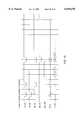
- DIMM 102is used to implement main computer memory only in pairs. Each DIMM of the pair provides half of a data word, such that the pair together is able to provide a very wide data word. This is illustrated in FIG. 3, in which a DIMM 102A and a DIMM 102B form a DIMM pair 302. As illustrated, DIMM 102A includes first memory bank portion 210A, second memory portion 212A, and first state memory 106A. Similarly, DIMM 102B includes first memory bank portion 210B, second memory bank portion 212B, and second state memory 106B.
- first memory bank portion 210A and second memory bank portion 212Bform a first memory bank, labeled bank 0. State information for data stored in bank 0 is maintained in state memory 106A. Second memory bank portion 212A and first memory bank portion 210B form a second memory bank, labeled bank 1. State memory 106B is configured to store state information corresponding to data stored in memory bank 1. As discussed in further detail below, a bank select signal is used to select one of bank 0 or bank 1 for data access operations. Memory bank 0 and memory bank 1 share common address and data lines.
- DIMM 102has a thirty-six (36) megabyte data storage capacity (including 32 megabytes of data and 4 megabytes of ECC) and a two (2) megabyte state information storage capacity. This embodiment yields a DIMM pair having sixty-four (64) megabytes of data storage capacity, eight (8) megabytes of ECC, and four (4) megabytes of state information storage capacity.
- DIMM 102has a seventy-two (72) megabyte data storage capacity (including 64 megabytes of data and 8 megabytes of ECC) and a four (4) megabyte state information storage capacity. This embodiment yields a DIMM pair having one hundred twenty-eight (128) megabytes of data storage capacity, sixteen (16) megabytes of ECC, and eight (8) megabytes of state information storage capacity.
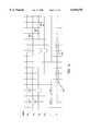
- FIG. 4is a block diagram illustrating interconnection of the components used to implement a DIMM 102 in accordance with the first preferred embodiment of the invention.
- Data memory 104is implemented using a plurality of synchronous, dynamic, random access memory (SDRAM) chips D0-D17.
- SDRAMs D0-D8represent memory chips of first memory bank portion 210
- SDRAMs D9-D17represent memory chips of second memory bank portion 212.
- each SDRAM D0-D17is a two megabit by eight bit (2M ⁇ 8) SDRAM chip.
- each memory bank portion 210,212is two (2) megabits deep by seventy-two (72) bits wide, yielding a total data capacity for data memory 104 of four (4) megabits deep by seventy-two (72) bits wide (i.e., 64 bits for data and 8 bits for ECC).
- State memory 106is implemented using a single one megabit by sixteen (1M ⁇ 16) bit SDRAM chip.
- Each DRAM chip D0-D17provides an 8-bit data word.
- data path 110provides an 8-bit data path DQ.
- one chip from each of memory bank portions 210,212is connected to an 8-bit data path DQ.
- SDRAM D0 and SDRAM D9are both connected to DQ[7:0]. Which chip is actually active on the data path is determined by an external chip or bank select signal (discussed below).
- Address and control buffers 214,216receive 20-bits of address and control signals, labeled A[19:0], buffers the address and control signals, and provides the address and control signal to SDRAMs D0-D17 as follows.
- Address and control buffer 214provides address and control signals (i.e., row address strobe, column address strobe, write enable and data mask) to left sides of bank portions 210,212 (i.e., SDRAMs D0-D3 and D9-D12) via bus 113.
- address and control buffer 214provides a bank select signal (CS0 -- ) and a clock enable signal (CKE0) to both the left and right sides of first bank portion 210 (i.e., SDRAMS D0-D8) via lines 117.
- CS0 --bank select signal
- CKE0clock enable signal
- Address and control buffer 216provides address and control signals (i.e., row address strobe, column address strobe, write enable and data mask) to right sides of bank portions 210,212 (i.e., SDRAMs D4-D8 and D13-D17) via bus 115.
- address and control buffer 216provides a bank select signal (CS1 -- ) and a clock enable signal (CKE1) to both the left and right sides of second bank portion 212 (i.e., SDRAMS D9-D17) via lines 119.
- Address and control signals A[19:0]are described further below in Table 1.
- Clock driver circuit 218provides clock signal 222 to each of SDRAMs D0-D17 and to the SDRAM of state memory 106.
- Clock driver circuit 218generates clock signal 222 based on clock control signals C[5:0].
- the clock control signals C[5:0]are described in further detail below.
- the data path 114 and address and control path 116 of state memory 106are illustrated by lines DIR -- DQ[15:0] and B[17:0], respectively. These signals are also described in further detail below.
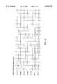
- the 72 megabyte embodiment of DIMM 102is depicted in FIG. 5.
- the DIMMis implemented using thirty-six (36) four megabit by 4 bit (4M ⁇ 4) SDRAMs.
- a second circuit board 500is used. Eighteen of the 4M ⁇ 4 SDRAMs (D0-D17) are mounted on a first circuit board 103. The other eighteen 4M ⁇ 4 SDRAMs (D18-D35) are mounted on second circuit board 500.
- Circuit board 500is mounted on circuit board 103 in a piggy-back fashion. Only circuit board 103 includes edge connector 108 (not shown in FIG. 5).
- All electrical connections to the SDRAM chips of circuit board 500occur through the edge connector of circuit board 103. Signals are shared by the two boards using a plurality of interconnecting pins. Each end of each pin is located in a plated through hole to provide electrical connections between the boards. These pins also physically attach the second board to the first board.
- An example of a piggy-back mounted circuit board(not using plated through holes) is provided in U.S. Pat. No. 5,200,917 to Shaffer et al.
- first memory bank portion 210is formed from the front side of each of circuit boards 103,500.
- SDRAM chips D0-D8 and D27-D35can be used to implement first memory bank portion 210.
- the back side of each circuit board 103,500can be used to implement second memory bank portion 212.
- the chips on each circuit board 103 and 500include on-board clocking and buffering via clock drivers 218A,218B and address and control buffers 214A,214B,216A,216B.
- each SDRAM chipis coupled to a 4-bit data path rather than an 8-bit data path.
- a bank select signal(one of signals A[19:0]) is used to select between memory bank portion 210 and memory bank portion 212.
- FIGS. 6A and 6BA preferred implementation of the 32 megabyte DIMM embodiment is depicted in FIGS. 6A and 6B.
- FIG. 6Ashows front side 202 of DIMM 102.
- FIG. 6Bshows back side 204 of DIMM 102.
- circuit board 103is approximately 1.34 inches high by 6.6 inches long and includes a 122 pad long by 2 pad wide edge connector along one longitudinal edge of the circuit board.
- SDRAMs D0-D8, SDRAM DIR0 (for state memory 106), data and control buffers 214A and clock driver 218Aare mounted on the front side 202 of circuit board 103.
- SDRAMs D9-D17 and data and control buffer 216Aare mounted on the back side 204 of circuit board 103.
- FIGS. 6A and 6Bare representative of the 72 megabyte embodiment of the invention as well as the 32 megabyte embodiment with the following differences.
- SDRAMs D0-D17are 4M ⁇ 4 devices instead of 2M ⁇ 8 bit devices.
- the directory memory chip(indicated as DIR 0) is a 2M ⁇ 8 bit device instead of a 1M ⁇ 16 bit device.
- a second 2M ⁇ 8 bit SDRAM chip(indicated by dashed lines in FIG. 6B as DIR 1) is used with DIR 0 to implement state memory 106.
- FIGS. 7A and 7BA preferred implementation of the piggy-backed second circuit board 500 of the 72 megabyte DIMM embodiment is depicted in FIGS. 7A and 7B.
- FIG. 7Ashows a front side 702 of second circuit board 500.
- FIG. 7Bshows a back side 704 of second circuit board 500.
- circuit board 500is approximately 1.16 inches high by 6.6 inches long and includes 116 interconnecting pins (not shown) providing electrical connections with circuit board 103.
- SDRAMs D18-D26, data and control buffer 214B and clock driver 218Bare mounted on the front side 702 of circuit board 500.
- SDRAMs D27-D35 and data and control buffer 216Bare mounted on the back side 704 of circuit board 500.
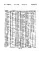
- Table 1lists the pad name and functions for the edge connector's pads according to a preferred embodiment of the present invention.
- the left-hand columnlists the abbreviated pad names and the right-hand column lists the function of the pads listed in the associated row of the table.
- the first pad descriptionis for the address pads and is abbreviated A[11:0].
- A[11:0]During row addressing the eleven least significant bits are used.
- the nine least significant bitsare used in the 36 MB DIMM embodiment, and the ten least significant bits are used in the 72 MB DIMM embodiment.
- the most significant bit (A11)is used to select between internal SDRAM banks. (These "internal banks” are different banks than banks zero and bank one of SDRAM DIMM 102 described above. Therefore, banks zero and one will hereafter be referred to as “external” banks that are selected via external back chip select signals CS1 and CS0, to distinguish them from the "internal SDRAM bank select" signal A11. This naming convention applies for SDRAMs used for data, as well as those used to store state information.)
- Datais input to, and output from the data memory of the SDRAM DIMM via 72 data input/output (I/O) paths abbreviated DQ[71:0]. Since the SDRAM DIMMs are used in pairs, a single access of the data memory on a single DIMM provides 72 bits, which when concatenated with 72 bits of the paired DIMM, yields a 144 bit data word that includes 128 bits of data an 16 bits of ECC.
- Two external bank chip select pads abbreviated CS1 -- and CS0 -- , a row address strobe command pad abbreviated RE -- , a column address strobe command pad abbreviated CE -- and a write-enable command pad abbreviated WE --are standard signals used for selecting, addressing, and write-enabling SDRAM chips, as would be apparent to a person skilled in the relevant art.
- two padsare provided for memory clock enable for the two banks of SDRAMs, respectively, and are abbreviated CKE1 and CKE0.
- a single input/output mask pathis also provided, and is abbreviated DQM. The function of the DQM mask pad will be described below in connection with the waveform diagrams.
- DIR -- A[11:0]The pads for the state memory of the SDRAM DIMM will now be described.
- the collection of directory address padsare abbreviated DIR -- A[11:0].
- Row addressing for the state memoryuses directory address bits A[10:0] and column addressing utilizes directory address bits A[7:0] for a 32 MB DIMM and bits A[8:0] for a 72 MB DIMM.
- a twelfth directory address pad (A11)is used for internal SDRAM bank selection.
- the next five pads listed in Table 1have similar functionalities as described above in connection with the analogous paths for the data memory section of the SDRAM DIMM.
- the directory chip select padis abbreviated DIR -- CS -- .
- a directory row address strobe command padis abbreviated DIR -- RE -- .
- a directory column address strobe command padis abbreviated DIR -- CE -- .
- a directory write-enable command padis abbreviated DIR -- WE -- .
- a directory input/output mask padis abbreviated DIR -- DQM.
- An additional directory clock-enable pad, abbreviated DIR -- CKEis provided for enabling the state memory clock.
- a Motorola, Inc.(Phoenix, Ariz.) MPC931 PLL chip, is used as a clock driver circuit. Because this specific integrated circuit supports both low voltage transistor-transistor-logic (LVTTL) or low voltage positive emitter coupled logic (LVPECL) respectively, the SDRAM DIMM of the present invention can include pads to facilitate either type of logic level for the clock driver circuit. Therefore, differential LVPECL clock pads abbreviated PCLK and PCLK -- are provided. Additionally, a LVTTL clock pad abbreviated TCLK is also provided. To select between the two possible power pad inputs, a select pad abbreviated TCLK -- SEL is provided.
- the logical voltage value applied to the TCLK -- SEL padwill select which voltage pads that the clock driver circuit will use. For example, the TCLK can be selected when the TCLK -- SEL pad is a logic high and the PCLK pad can be used for powering the clock driver circuit when the TCLK -- SEL pad is at a low logic level.
- Another padenables the phase lock loop portion of the clock driver circuit, and is abbreviated PLL -- EN. Reset and tri-state clock driver circuit outputs for this manufacturers' chip can be selected via another pad abbreviated PLL -- CLR.
- PLL -- CLRPhase locked loop
- a power supply voltagee.g., 3.3 V.D.C.
- groundare supplied via pads abbreviated V3 and GND respectively. If implemented, a single additional pad is used to read the contents of the serial programmable read-only memory (PROM), which is labeled SERIAL -- DAT.
- PROMserial programmable read-only memory
- FIG. 15illustrates a preferred exemplary pad assignment for the entire 244 connector pad edge connector 108. This figure is broken-down into 6 columns in order to show all 244 pad assignments on a single page. 14 pads are unassigned. Each column shows the pad number assignment followed by the abbreviation of the pad description corresponding to the pad names listed in Table 1. The pad assignments are made taking trace lengths on the PCB 103 into consideration to minimize signal skew and loading.
- Table 2shows representative timing requirements for an exemplary SDRAM DIMM pair using NEC Corporation (Japan) part numbers uPD4516421GS-A12-TJF (4M ⁇ 4), uPD4516421GS-A12-TJF (2M ⁇ 8) or uPD45161GS-A12-TJF (1M ⁇ 16).
- the timing requirements listed in Table 2are for nominal temperatures between 0 and 70° C. and a power supply voltage of between 3.3 volts and 3.6 V.D.C., with all clock references to PCLK.
- the timing requirements of Table 2include clock jitter and skew of approximately 1.5 nanoseconds.
- the timing parameters shown in Table 2generally represent time periods as measured at the edge connector, ignoring any small effects the connector itself will have on the signals. These times would appear different if measured at a location on the SDRAMs themselves.
- the row and column addressesare set by a memory system into which the SDRAM DIMMs are connected and as required by the specific SDRAM devices employed on the DIMMs.
- FIGS. 8-13The timing diagrams for reading and writing information for the SDRAM DIMM are shown in FIGS. 8-13.
- FIG. 8shows a representative "data read” timing diagram according to the present invention.
- FIG. 9shows a representative "data write” timing diagram according to the present invention.
- FIG. 10shows a representative "read modify write” (RMW) timing diagram according to the present invention.
- the vertical barsrepresent clock edges, at which the control and address signals are sampled by the SDRAM parts.
- FIG. 8a total of six timing traces are illustrate, including: chip select (CS -- ) 802; row address strobe (RE -- ) 804; column address strobe (CE -- ) 806; write-enable (WE -- ) 808; address (A) inputs 810; and, data (DQ) inputs/outputs 812.
- the SDRAM DIMMs data output 812represents the timing of an output based on application of the row and column addresses and assertion of the RE_ CE -- and WE -- control signals.
- the data memoryis arranged so that a single row access can be followed by four column addresses (C0, C2, C4 and C6) to access a block of data from a DIMM pair.
- a block of data(not including parity/ECC data) is 8 words by 16 bytes, or a total of 128 bytes (which is 64 bits per DIMM or a total of 128 bits per location access, since the pair is accessed in parallel). So for 4 consecutive location accesses per RA, a total of 8 data words D0-D7 by 16 bytes are output.
- the SDRAM DIMM pairis written to in block writes as illustrated by trace 902 in FIG. 9.
- Table 3shows representative cycle latency for various timing parameters of FIGS. 8-10. These parameter latencies are listed in nanosecond and are nominal.
- Read modify writescan also be done on data, as shown in FIG. 10.
- a locationis accessed by a single RE -- and CE -- (traces 1002 and 1004 respectively) and the data is read at the first D0/D1 pair 1006. After the data is modified it is written back as shown by the second D0/D1 pair (1008) to the DIMM pair by asserting the CE -- and the WE -- (trace 1010) signals.
- the state memoryis accessed in parallel with the data memory.
- a state memorycomprises two reads and two writes, since each directory entry is 32 bits wide, and each state memory in the preferred embodiment implements SDRAMs that are only 16 bits deep.
- page migration incrementingrequires reading the location that corresponds to the block being accessed for both the node making the request and the home node, and a write to increment the count for the node making the request.
- the page migration countskeep track of the number of times a node accesses a particular page of memory. Thus, that count must be incremented each time a page is accessed.
- the pageis migrated to the memory associated with that node.
- a more detailed description of page migrationis found in the co-pending application (Attorney Docket No. 1452.0690000) noted above.
- the corresponding state memoryis read a total of 4 times and written to a total of 3 times, so that accesses to the data and state information is balanced.
- FIGS. 11, 12 and 13show three separate waveform diagrams involving data masking, including reads, writes, and revisions, respectively.
- the following signalsare shown: chip select (DIR -- CS -- ), row address strobe (DIR -- RE -- ), column address strobe (DIR -- CE -- ), write enable (DIR -- WE -- ), input/output data masks (DIR -- DQM), address A inputs and data (DIR -- DQ) input/outputs.
- the directory cycle for a readstarts by reading the first half of the directory word (D0), the page migration count for the requesting node (S), the second half of the directory word (D1), the home node's page migration count (H), then after a dead cycle on DIR -- DQ, the new page migration count (S) and the new directory information (D0 and D1) are written into the state memory.
- the informationis read out in the listed order due to requirements of the memory controller that lead to the quickest memory response time.
- FIG. 12is a slight permutation of the waveforms shown in FIG. 11. The order of S and D0 are switched in this figure in contrast to FIG. 11.
- FIG. 13shows the state access for a state revision operation, which is a state-only access and does not require a memory access. To minimize the overhead of these revisions operations only the directory information is accessed.
- the DIMM pairs of the inventionare used to implement main memory.
- Each processor node of the DSM multiprocessorincludes a portion of main memory.
- the state memory configurations discussedprovide sufficient capacity to accommodate the state information required for a system having 16 nodes.
- each state memory described aboveincludes 16 bit wide words of state information.
- additional state memoryis required at each node to accommodate more state information about caching, because more cache memories are likely added to the system.
- the additional state memorycan be provided by using a state memory-only DIMM. According to a preferred embodiment of this aspect of the present invention, this state memory-only DIMM adds 32 bits of additional state memory. The resulting total state memory provides 48 bit wide words of state information (16 original bits on the SDRAM data/state memory DIMM plus 32 bits from the state memory-only DIMM).
- the DSM multiprocessorcan accommodate up to 64 nodes using conventional bit-vectors and up to 512 nodes using flexible directory bit vectors. The specific number of additional state information bits can vary and is extendable, as would be apparent to a person of ordinary skill in the relevant art.
- FIG. 14The organization of DIMM pairs 302 and state memory-only DIMMs 1406 in a main memory portion 1400 of a node of a DSM multiprocessor is illustrated in FIG. 14.
- a memory/directory controller 1402 at the node of the DSM multiprocessorperforms all memory management functions for the data and state memory on the DIMMs 302 and 1406.
- a memory address and control buffer 1410buffers all address and control lines 1420 going to the data memories of the DIMM pairs 302 from the controller 1402.
- a state (directory) address and control buffer 1412buffers all address and control signals on lines 1422 going to the state memories of the state memory-only DIMM pairs 1406 from the controller 1402.
- Each state memory-only DIMM 1406can be implemented using a single PCB.
- the PCBcan be populated with SDRAM chips of similar or dissimilar capacity chips as the SDRAMs of the DIMMs 302.
- the SDRAMs of the state memory-only DIMMs 1406are organized with two banks of state memory so that state information and addressing of the state information is consistent with the directory (DIR)/state memories on the DIMMs 302.
- a bus exchanger 1408passes the 144 bit data word to/from each DIMM pair 302 via bidirectional buses 1409.
- the bus exchange 1408takes 144 bits data at the memory speed and converts it to 72 bits at twice the memory speed.
- the bus exchanger 1408is implemented with a part number SN74ALVC16282 (manufactured by Texas Instruments, Dallas Tex.) that converts 144 bits at 50 MHz to 72 bits at 100 MHz, and vice versa for bidirectional transfer of the data between the DIMMS 302 and the controller 1402, via bidirectonal bus 1411. Directory data is not buffered, and is transferred between the state memory-only DIMMs 1406 and the controller 1402 via bidirectional bus 1424.
- DIMM of the inventionmay be produced in other data capacities. For example, using 64 megabit (i.e., 8M ⁇ 8) SDRAM chips, a single board DIMM may be produced having 128 megabyte data and 16 megabyte ECC (18 chips ⁇ 8 megabytes per chip) storage capacity (including data and ECC). This would yield a DIMM pair having 256 megabytes of data storage capacity.
- the 64 megabyte SDRAM chipscan be used to implement a 256 megabyte data and 32 megabyte ECC DIMM and a 512 megabyte data, 64 megabyte ECC DIMM pair.
- a piggy-back boardis used to allow the DIMM to accommodate 36 SDRAMs for the data memory.
- chip stacking techniquesmay also be used to accommodate 36 SDRAM chips. If chip stacking techniques are used, the piggy-board may be eliminated.
- 4 megabit (i.e., 1M ⁇ 1) SDRAM chipscan be combined to produce DIMMs with lower storage capacity, or the above-described stacking and/or piggy-back techniques can be used for higher storage capacity.
Landscapes
- Engineering & Computer Science (AREA)
- Theoretical Computer Science (AREA)
- Physics & Mathematics (AREA)
- General Engineering & Computer Science (AREA)
- General Physics & Mathematics (AREA)
- Dram (AREA)
- Memory System (AREA)
- Memory System Of A Hierarchy Structure (AREA)
- Multi Processors (AREA)
Abstract
Description
TABLE 1 ______________________________________ Pad Description Pad Name Function ______________________________________ A[11:0].sup.A Data Memory Address (Row:A[10:0]; Col:A[9:0]; Bank select: A11) DQ[71:0] Data I/O Pads for Data Memory CS1.sub.--, CS0.sub.-- .sup.A Chip select for Data Memory SDRAMs RE.sub.-- .sup.A Row address stobe (RAS) command for Data Memory CE.sub.-- .sup.A Column address strobe (CAS) command for Data Memory WE.sub.-- .sup.A Write enable command for Data Memory DQM.sup.A Input/Output mask for Data Memory CKE1, CKE0.sup.A Memory clock enable for CS1 and CS0 SDRAM's respectively DIR.sub.-- A[11:0].sup.B State Memory Address (Row:A[10:0]; Col:A[7:0]; Bank select: A11) DIR.sub.-- DQ[15:0] Directory data (i.e., state information) I/O for State Memory DIR.sub.-- CS.sup.B Directory chip select for State Memory DIR.sub.-- RE.sup.B Directory row address strobe command for State Memory DIR.sub.-- CE.sup.B Directory column address strobe command for State Memory DIR.sub.-- WE.sub.-- .sup.B Directory write enable command for State Memory DIR.sub.-- DQM.sup.B Directory input/output mask for State Memory DIR.sub.-- CKE.sup.B Directory clock enable for State Memory PCLK, PCLK.sub.-- .sup.C Differential LVPECL clock inputs TCLK.sup.C LVTTL clock inputs TCLK.sub.-- SEL.sup.C Selects TCLK when high and PCLK when low PLL.sub.-- EN.sup.C Enables PLL on clock driver PLL.sub.-- CLR.sup.C PLL reset and tri-state clock driver outputs V3 Power supply (3.3VD.C.) GND Ground SERIAL.sub.-- DAT Line to read contents of serial prom ______________________________________ .sup.A = These pads are shown collectively on FIGS. 4 and 5 as A [19:0 .sup.B = These pads are shown collectively on FIGS. 4 and 5 as B [17:0 .sup.C = These pads are shown collectively on FIGS. 4 and 5 as C [5:0
TABLE 2 ______________________________________ Timing Requirements ______________________________________ (Ta = 0 to 70C, VDD, VDDQ = 3.15VDC to 3.6VDC) All clock references (Ref) are to PCLK. The timings include a clock jitter + skew of 1.5 nsmax 1. Clock cycle time = 20 nsmax 2. Clock to data in setup = 4.5 nsmin 3. Clock to data in hold = 2.5 nsmin 4. Set up time input address = 12.0 nsmin 5. Hold time input address = 1.0 nsmin 6. Set up time input command = 12.0 nsmin 7. Hold time input command = 1 nsmin 8. Access time from clock (CAS latency = 2) = 15 ns max, load 80pf 9. Hold time output data = 1.5 nsmin 10. Clock to data out, high impendance = 16.5 ns max, load 80pf 11. Clock to CKE setup (power down exit) = 12.0 nsmax 12. Clock CKE hold = 1.0 nsmin 13. Ref/active to Ref/active command period = 110 nsmin 14. Active to precharge command period = 75 ns min - 10000 nsmax 15. Active command to column command (same bank) = 38 nsmin 16. Precharge to active command period = 38 nsmin 17. Last data in to precharge lead time = 18 nsmin 18. Refresh period = 64 ms max ______________________________________
TABLE 3 ______________________________________ Cycle Latency at 50 MHZ ______________________________________ 1. CAS latency = 2 (number of clock between CE.sub.-- command and data is available). 2. tRCD = 2 (minimum number of clocks between RE.sub.-- and CE.sub.-- commands). 3. RAS latency = 4 (minimum number of clocks between RE.sub.-- and data is available). 4. tRC = 6 (minimum number of clocks between refresh and RE.sub.-- command). 5. tRAS = 4 (minimum number of clocks between RE.sub.-- and precharging). 6. tRRD = 2 (minimum number of clocks between RE.sub.-- commands). 7. tRP = 2 (minimum number of clocks between precharging and RE.sub.-- command). 8. tDPL = 1 (minimum number of clocks between data in the pre- charging command). 9. tDAL = 3 (minimum number of clocks between data in and RE.sub.-- for auto-precharging). ______________________________________
Claims (8)
Priority Applications (1)
| Application Number | Priority Date | Filing Date | Title |
|---|---|---|---|
| US09/126,944US6049476A (en) | 1995-05-15 | 1998-07-31 | High memory capacity DIMM with data and state memory |
Applications Claiming Priority (3)
| Application Number | Priority Date | Filing Date | Title |
|---|---|---|---|
| US44021495A | 1995-05-15 | 1995-05-15 | |
| US08/747,975US5790447A (en) | 1995-05-15 | 1996-11-12 | High-memory capacity DIMM with data and state memory |
| US09/126,944US6049476A (en) | 1995-05-15 | 1998-07-31 | High memory capacity DIMM with data and state memory |
Related Parent Applications (1)
| Application Number | Title | Priority Date | Filing Date |
|---|---|---|---|
| US08/747,975ContinuationUS5790447A (en) | 1995-05-15 | 1996-11-12 | High-memory capacity DIMM with data and state memory |
Publications (1)
| Publication Number | Publication Date |
|---|---|
| US6049476Atrue US6049476A (en) | 2000-04-11 |
Family
ID=23747896
Family Applications (2)
| Application Number | Title | Priority Date | Filing Date |
|---|---|---|---|
| US08/747,975Expired - LifetimeUS5790447A (en) | 1995-05-15 | 1996-11-12 | High-memory capacity DIMM with data and state memory |
| US09/126,944Expired - LifetimeUS6049476A (en) | 1995-05-15 | 1998-07-31 | High memory capacity DIMM with data and state memory |
Family Applications Before (1)
| Application Number | Title | Priority Date | Filing Date |
|---|---|---|---|
| US08/747,975Expired - LifetimeUS5790447A (en) | 1995-05-15 | 1996-11-12 | High-memory capacity DIMM with data and state memory |
Country Status (10)
| Country | Link |
|---|---|
| US (2) | US5790447A (en) |
| EP (2) | EP0744748B1 (en) |
| JP (2) | JP4020271B2 (en) |
| KR (1) | KR100215267B1 (en) |
| CN (1) | CN1142635A (en) |
| AU (1) | AU707453B2 (en) |
| CA (1) | CA2176642A1 (en) |
| DE (2) | DE69610662T2 (en) |
| IN (1) | IN188196B (en) |
| TW (1) | TW303433B (en) |
Cited By (89)
| Publication number | Priority date | Publication date | Assignee | Title |
|---|---|---|---|---|
| US6266265B1 (en)* | 1999-05-17 | 2001-07-24 | Nec Corporation | Memory module using a vacant pin terminal for balancing parasitic capacitive loads |
| WO2002008910A1 (en)* | 2000-07-20 | 2002-01-31 | Silicon Graphics, Inc. | Memory device storing data and directory information thereon, and method for providing the directory information and the data in the memory device |
| US6347367B1 (en)* | 1999-01-29 | 2002-02-12 | International Business Machines Corp. | Data bus structure for use with multiple memory storage and driver receiver technologies and a method of operating such structures |
| US6349050B1 (en)* | 2000-10-10 | 2002-02-19 | Rambus, Inc. | Methods and systems for reducing heat flux in memory systems |
| US6362997B1 (en)* | 2000-10-16 | 2002-03-26 | Nvidia | Memory system for use on a circuit board in which the number of loads are minimized |
| US6407940B1 (en)* | 2000-09-29 | 2002-06-18 | Kabushiki Kaisha Toshiba | Memory card device including a clock generator |
| US6415364B1 (en)* | 1997-12-31 | 2002-07-02 | Unisys Corporation | High-speed memory storage unit for a multiprocessor system having integrated directory and data storage subsystems |
| US6549420B2 (en)* | 1996-10-31 | 2003-04-15 | Hewlett-Packard Development Company, L.P. | Method and apparatus for increasing memory capacity |
| US20030090879A1 (en)* | 2001-06-14 | 2003-05-15 | Doblar Drew G. | Dual inline memory module |
| US20030163543A1 (en)* | 2002-02-28 | 2003-08-28 | Silicon Graphics, Inc. | Method and system for cache coherence in DSM multiprocessor system without growth of the sharing vector |
| US20030161198A1 (en)* | 2002-02-26 | 2003-08-28 | Peddle Charles I. | Method and apparatus for implementing a selectively operable clock booster for DDR memory or other logic modules which utilize partially-defective memory parts, or a combination of partially-defective and flawless memory parts |
| US20040100812A1 (en)* | 2002-11-22 | 2004-05-27 | Wu Chung-Hsiao R. | Circuit topology for high speed memory access |
| US20040136229A1 (en)* | 2002-03-07 | 2004-07-15 | Bhakta Jayesh R. | Arrangement of integrated circuits in a memory module |
| US20040225853A1 (en)* | 2003-05-08 | 2004-11-11 | Lee Terry R. | Apparatus and methods for a physical layout of simultaneously sub-accessible memory modules |
| US20050018495A1 (en)* | 2004-01-29 | 2005-01-27 | Netlist, Inc. | Arrangement of integrated circuits in a memory module |
| US6868485B1 (en)* | 2002-09-27 | 2005-03-15 | Advanced Micro Devices, Inc. | Computer system with integrated directory and processor cache |
| US20050071580A1 (en)* | 2003-09-30 | 2005-03-31 | Intel Corporation | Distributed memory initialization and test methods and apparatus |
| US20050097264A1 (en)* | 2003-10-31 | 2005-05-05 | Park Kwang-Soo | Memory module with registers |
| US20050144383A1 (en)* | 2003-12-25 | 2005-06-30 | Seiichi Higaki | Memory control device and method for controlling the same |
| US20060023482A1 (en)* | 2004-07-30 | 2006-02-02 | International Business Machines Corporation | 276-Pin buffered memory module with enhanced fault tolerance |
| US20060036827A1 (en)* | 2004-07-30 | 2006-02-16 | International Business Machines Corporation | System, method and storage medium for providing segment level sparing |
| US20060095629A1 (en)* | 2004-10-29 | 2006-05-04 | International Business Machines Corporation | System, method and storage medium for providing a service interface to a memory system |
| US20060095620A1 (en)* | 2004-10-29 | 2006-05-04 | International Business Machines Corporation | System, method and storage medium for merging bus data in a memory subsystem |
| US20060095646A1 (en)* | 2004-10-29 | 2006-05-04 | International Business Machines Corporation | System, method and storage medium for a memory subsystem command interface |
| US20060095703A1 (en)* | 2004-10-29 | 2006-05-04 | International Business Machines Corporation | System, method and storage medium for bus calibration in a memory subsystem |
| US20060095701A1 (en)* | 2004-10-29 | 2006-05-04 | International Business Machines Corporation | System, method and storage medium for a memory subsystem with positional read data latency |
| US20060107175A1 (en)* | 2004-10-29 | 2006-05-18 | International Business Machines Corporation | System, method and storage medium for providing fault detection and correction in a memory subsystem |
| US20060107186A1 (en)* | 2004-10-29 | 2006-05-18 | International Business Machines Corporation | System, method and storage medium for providing a high speed test interface to a memory subsystem |
| US20060117233A1 (en)* | 2004-10-29 | 2006-06-01 | International Business Machines Corporation | System, Method and storage medium for testing a memory module |
| US20060118950A1 (en)* | 2003-07-03 | 2006-06-08 | Smart Modular Technologies, Inc., A California Corporation | Multi function module |
| US20060136618A1 (en)* | 2004-07-30 | 2006-06-22 | International Business Machines Corporation | System, method and storage medium for a multi-mode memory buffer device |
| US7096323B1 (en) | 2002-09-27 | 2006-08-22 | Advanced Micro Devices, Inc. | Computer system with processor cache that stores remote cache presence information |
| US20060190780A1 (en)* | 2003-04-14 | 2006-08-24 | Gower Kevin C | High reliability memory module with a fault tolerant address and command bus |
| US7117421B1 (en)* | 2002-05-31 | 2006-10-03 | Nvidia Corporation | Transparent error correction code memory system and method |
| US20070033490A1 (en)* | 2005-07-19 | 2007-02-08 | Karl-Heinz Moosrainer | Semiconductor memory module with error correction |
| US20070101086A1 (en)* | 2005-10-31 | 2007-05-03 | International Business Machines Corporation | System, method and storage medium for deriving clocks in a memory system |
| US20070160053A1 (en)* | 2005-11-28 | 2007-07-12 | Coteus Paul W | Method and system for providing indeterminate read data latency in a memory system |
| US20070223159A1 (en)* | 2000-05-03 | 2007-09-27 | Belgacem Haba | Semiconductor Module with Serial Bus Connection to Multiple Dies |
| US7277988B2 (en) | 2004-10-29 | 2007-10-02 | International Business Machines Corporation | System, method and storage medium for providing data caching and data compression in a memory subsystem |
| US20070255902A1 (en)* | 2004-07-30 | 2007-11-01 | International Business Machines Corporation | System, method and storage medium for providing a serialized memory interface with a bus repeater |
| US20070276976A1 (en)* | 2006-05-24 | 2007-11-29 | International Business Machines Corporation | Systems and methods for providing distributed technology independent memory controllers |
| US20070276977A1 (en)* | 2006-05-24 | 2007-11-29 | International Business Machines Corporation | Systems and methods for providing memory modules with multiple hub devices |
| US20080002447A1 (en)* | 2006-06-29 | 2008-01-03 | Smart Modular Technologies, Inc. | Memory supermodule utilizing point to point serial data links |
| US20080034148A1 (en)* | 2006-08-01 | 2008-02-07 | International Business Machines Corporation | Systems and methods for providing performance monitoring in a memory system |
| US20080040563A1 (en)* | 2006-08-10 | 2008-02-14 | International Business Machines Corporation | Systems and methods for memory module power management |
| US20080094811A1 (en)* | 2006-10-23 | 2008-04-24 | International Business Machines Corporation | High density high reliability memory module with a fault tolerant address and command bus |
| US20080115137A1 (en)* | 2006-08-02 | 2008-05-15 | International Business Machines Corporation | Systems and methods for providing collision detection in a memory system |
| US20080133939A1 (en)* | 2002-08-07 | 2008-06-05 | Radoslav Danilak | System and method for transparent disk encryption |
| US20080162991A1 (en)* | 2007-01-02 | 2008-07-03 | International Business Machines Corporation | Systems and methods for improving serviceability of a memory system |
| US20080183903A1 (en)* | 2007-01-29 | 2008-07-31 | International Business Machines Corporation | Systems and methods for providing dynamic memory pre-fetch |
| US7490217B2 (en) | 2006-08-15 | 2009-02-10 | International Business Machines Corporation | Design structure for selecting memory busses according to physical memory organization information stored in virtual address translation tables |
| US20090063730A1 (en)* | 2007-08-31 | 2009-03-05 | Gower Kevin C | System for Supporting Partial Cache Line Write Operations to a Memory Module to Reduce Write Data Traffic on a Memory Channel |
| US20090063784A1 (en)* | 2007-08-31 | 2009-03-05 | Gower Kevin C | System for Enhancing the Memory Bandwidth Available Through a Memory Module |
| US20090063787A1 (en)* | 2007-08-31 | 2009-03-05 | Gower Kevin C | Buffered Memory Module with Multiple Memory Device Data Interface Ports Supporting Double the Memory Capacity |
| US20090063729A1 (en)* | 2007-08-31 | 2009-03-05 | Gower Kevin C | System for Supporting Partial Cache Line Read Operations to a Memory Module to Reduce Read Data Traffic on a Memory Channel |
| US20090063761A1 (en)* | 2007-08-31 | 2009-03-05 | Gower Kevin C | Buffered Memory Module Supporting Two Independent Memory Channels |
| US20090063923A1 (en)* | 2007-08-31 | 2009-03-05 | Gower Kevin C | System and Method for Performing Error Correction at a Memory Device Level that is Transparent to a Memory Channel |
| US20090063731A1 (en)* | 2007-09-05 | 2009-03-05 | Gower Kevin C | Method for Supporting Partial Cache Line Read and Write Operations to a Memory Module to Reduce Read and Write Data Traffic on a Memory Channel |
| US20090063922A1 (en)* | 2007-08-31 | 2009-03-05 | Gower Kevin C | System for Performing Error Correction Operations in a Memory Hub Device of a Memory Module |
| US20090119114A1 (en)* | 2007-11-02 | 2009-05-07 | David Alaniz | Systems and Methods for Enabling Customer Service |
| US7539842B2 (en) | 2006-08-15 | 2009-05-26 | International Business Machines Corporation | Computer memory system for selecting memory buses according to physical memory organization information stored in virtual address translation tables |
| US20090190427A1 (en)* | 2008-01-24 | 2009-07-30 | Brittain Mark A | System to Enable a Memory Hub Device to Manage Thermal Conditions at a Memory Device Level Transparent to a Memory Controller |
| US20090193315A1 (en)* | 2008-01-24 | 2009-07-30 | Gower Kevin C | System for a Combined Error Correction Code and Cyclic Redundancy Check Code for a Memory Channel |
| US20090193200A1 (en)* | 2008-01-24 | 2009-07-30 | Brittain Mark A | System to Support a Full Asynchronous Interface within a Memory Hub Device |
| US20090193290A1 (en)* | 2008-01-24 | 2009-07-30 | Arimilli Ravi K | System and Method to Use Cache that is Embedded in a Memory Hub to Replace Failed Memory Cells in a Memory Subsystem |
| US20090193201A1 (en)* | 2008-01-24 | 2009-07-30 | Brittain Mark A | System to Increase the Overall Bandwidth of a Memory Channel By Allowing the Memory Channel to Operate at a Frequency Independent from a Memory Device Frequency |
| US20090193203A1 (en)* | 2008-01-24 | 2009-07-30 | Brittain Mark A | System to Reduce Latency by Running a Memory Channel Frequency Fully Asynchronous from a Memory Device Frequency |
| US7581073B2 (en) | 2006-08-09 | 2009-08-25 | International Business Machines Corporation | Systems and methods for providing distributed autonomous power management in a memory system |
| US7584336B2 (en) | 2006-06-08 | 2009-09-01 | International Business Machines Corporation | Systems and methods for providing data modification operations in memory subsystems |
| US20090237970A1 (en)* | 2008-03-19 | 2009-09-24 | Samsung Electronics Co., Ltd. | Process variation compensated multi-chip memory package |
| US7606988B2 (en) | 2007-01-29 | 2009-10-20 | International Business Machines Corporation | Systems and methods for providing a dynamic memory bank page policy |
| US7636813B2 (en) | 2006-05-22 | 2009-12-22 | International Business Machines Corporation | Systems and methods for providing remote pre-fetch buffers |
| US20100125771A1 (en)* | 2008-11-18 | 2010-05-20 | Fujitsu Limited | Error judging circuit and shared memory system |
| US20100269012A1 (en)* | 2006-10-23 | 2010-10-21 | International Business Machines Corporation | High Density High Reliability Memory Module with Power Gating and a Fault Tolerant Address and Command Bus |
| US20110004709A1 (en)* | 2007-09-05 | 2011-01-06 | Gower Kevin C | Method for Enhancing the Memory Bandwidth Available Through a Memory Module |
| US7899983B2 (en) | 2007-08-31 | 2011-03-01 | International Business Machines Corporation | Buffered memory module supporting double the memory device data width in the same physical space as a conventional memory module |
| US7930469B2 (en) | 2008-01-24 | 2011-04-19 | International Business Machines Corporation | System to provide memory system power reduction without reducing overall memory system performance |
| US8290919B1 (en) | 2010-08-27 | 2012-10-16 | Disney Enterprises, Inc. | System and method for distributing and accessing files in a distributed storage system |
| US8392368B1 (en)* | 2010-08-27 | 2013-03-05 | Disney Enterprises, Inc. | System and method for distributing and accessing files in a distributed storage system |
| US20130271910A1 (en)* | 2008-11-13 | 2013-10-17 | Mosaid Technologies Incorporated | System including a plurality of encapsulated semiconductor chips |
| US8768981B1 (en) | 2010-08-27 | 2014-07-01 | Disney Enterprises, Inc. | System and method for distributing and accessing files in a distributed storage system |
| KR101463375B1 (en) | 2005-06-24 | 2014-11-18 | 구글 인코포레이티드 | An integrated memory core and memory interface circuit |
| US8947951B2 (en) | 2012-06-22 | 2015-02-03 | Samsung Electronics Co., Ltd. | Semiconductor memory devices |
| US9494740B2 (en) | 2012-01-31 | 2016-11-15 | Hewlett Packard Enterprise Development Lp | Optical architecture with riser cards a matrix and optic cables to carry outbound signals of the matrix to the riser cards |
| CN108292518A (en)* | 2015-11-25 | 2018-07-17 | 英特尔公司 | Method and apparatus for reading memory cells based on clock pulse count |
| US10216659B2 (en) | 2014-05-30 | 2019-02-26 | Hewlett Packard Enterprise Development Lp | Memory access signal detection utilizing a tracer DIMM |
| US10248418B2 (en) | 2015-06-30 | 2019-04-02 | International Business Machines Corporation | Cleared memory indicator |
| US10635307B2 (en) | 2015-06-30 | 2020-04-28 | International Business Machines Corporation | Memory state indicator |
| US10884946B2 (en) | 2015-06-30 | 2021-01-05 | International Business Machines Corporation | Memory state indicator check operations |
Families Citing this family (70)
| Publication number | Priority date | Publication date | Assignee | Title |
|---|---|---|---|---|
| US5991850A (en)* | 1996-08-15 | 1999-11-23 | Micron Technology, Inc. | Synchronous DRAM modules including multiple clock out signals for increasing processing speed |
| US6006238A (en)* | 1997-01-31 | 1999-12-21 | Network Computing Devices, Inc. | Method and apparatus for migrating/shadowing data between a server and its clients |
| US5953215A (en)* | 1997-12-01 | 1999-09-14 | Karabatsos; Chris | Apparatus and method for improving computer memory speed and capacity |
| US6108228A (en)* | 1997-12-02 | 2000-08-22 | Micron Technology, Inc. | Quad in-line memory module |
| US7007130B1 (en)* | 1998-02-13 | 2006-02-28 | Intel Corporation | Memory system including a memory module having a memory module controller interfacing between a system memory controller and memory devices of the memory module |
| DE69836437T2 (en) | 1997-12-05 | 2007-09-27 | Intel Corporation, Santa Clara | STORAGE SYSTEM WITH MEMORY MODULE WITH A MEMORY MODULE CONTROL UNIT |
| US7024518B2 (en)* | 1998-02-13 | 2006-04-04 | Intel Corporation | Dual-port buffer-to-memory interface |
| US6968419B1 (en)* | 1998-02-13 | 2005-11-22 | Intel Corporation | Memory module having a memory module controller controlling memory transactions for a plurality of memory devices |
| US6970968B1 (en)* | 1998-02-13 | 2005-11-29 | Intel Corporation | Memory module controller for providing an interface between a system memory controller and a plurality of memory devices on a memory module |
| US6154821A (en)* | 1998-03-10 | 2000-11-28 | Rambus Inc. | Method and apparatus for initializing dynamic random access memory (DRAM) devices by levelizing a read domain |
| US5982654A (en)* | 1998-07-20 | 1999-11-09 | Micron Technology, Inc. | System for connecting semiconductor devices |
| US6347394B1 (en)* | 1998-11-04 | 2002-02-12 | Micron Technology, Inc. | Buffering circuit embedded in an integrated circuit device module used for buffering clocks and other input signals |
| KR100308214B1 (en)* | 1998-12-30 | 2001-12-17 | 윤종용 | Dual chip semiconductor integrated circuit device |
| US6115278A (en)* | 1999-02-09 | 2000-09-05 | Silicon Graphics, Inc. | Memory system with switching for data isolation |
| US6338144B2 (en)* | 1999-02-19 | 2002-01-08 | Sun Microsystems, Inc. | Computer system providing low skew clock signals to a synchronous memory unit |
| US6414868B1 (en) | 1999-06-07 | 2002-07-02 | Sun Microsystems, Inc. | Memory expansion module including multiple memory banks and a bank control circuit |
| US6683372B1 (en) | 1999-11-18 | 2004-01-27 | Sun Microsystems, Inc. | Memory expansion module with stacked memory packages and a serial storage unit |
| US6772261B1 (en) | 2000-04-27 | 2004-08-03 | International Business Machines Corporation | Interface that allows testing and using memory modules in computer systems not designed for the modules |
| JP4480855B2 (en)* | 2000-06-08 | 2010-06-16 | 富士通マイクロエレクトロニクス株式会社 | Module including semiconductor device and system including module |
| KR100335504B1 (en)* | 2000-06-30 | 2002-05-09 | 윤종용 | 2 Channel memory system having shared control and address bus and memory modules used therein |
| US6487102B1 (en) | 2000-09-18 | 2002-11-26 | Intel Corporation | Memory module having buffer for isolating stacked memory devices |
| TW528948B (en)* | 2000-09-14 | 2003-04-21 | Intel Corp | Memory module having buffer for isolating stacked memory devices |
| US6530006B1 (en)* | 2000-09-18 | 2003-03-04 | Intel Corporation | System and method for providing reliable transmission in a buffered memory system |
| US6658530B1 (en)* | 2000-10-12 | 2003-12-02 | Sun Microsystems, Inc. | High-performance memory module |
| EP1466326A2 (en)* | 2001-01-17 | 2004-10-13 | Honeywell International Inc. | Enhanced memory module architecture |
| US6721185B2 (en) | 2001-05-01 | 2004-04-13 | Sun Microsystems, Inc. | Memory module having balanced data I/O contacts pads |
| US6714433B2 (en)* | 2001-06-15 | 2004-03-30 | Sun Microsystems, Inc. | Memory module with equal driver loading |
| DE10142361B4 (en)* | 2001-08-30 | 2011-05-05 | Qimonda Ag | memory module |
| DE10149031A1 (en)* | 2001-10-05 | 2003-04-24 | Infineon Technologies Ag | Dynamic random access memory has read clock generator which is arranged in memory module, so that data bus and read clock bus are substantially symmetric |
| US6956284B2 (en) | 2001-10-26 | 2005-10-18 | Staktek Group L.P. | Integrated circuit stacking system and method |
| US7202555B2 (en) | 2001-10-26 | 2007-04-10 | Staktek Group L.P. | Pitch change and chip scale stacking system and method |
| US7656678B2 (en) | 2001-10-26 | 2010-02-02 | Entorian Technologies, Lp | Stacked module systems |
| US7081373B2 (en) | 2001-12-14 | 2006-07-25 | Staktek Group, L.P. | CSP chip stack with flex circuit |
| US7096407B2 (en)* | 2003-02-18 | 2006-08-22 | Hewlett-Packard Development Company, L.P. | Technique for implementing chipkill in a memory system |
| US20040201968A1 (en)* | 2003-04-09 | 2004-10-14 | Eric Tafolla | Multi-bank memory module |
| DE60305006T2 (en)* | 2003-05-08 | 2006-11-02 | Infineon Technologies Ag | CIRCUIT MODULE WITH CLOSED GROUPS OF OVERLAPPING SEMICONDUCTOR CHIPS |
| US7392347B2 (en) | 2003-05-10 | 2008-06-24 | Hewlett-Packard Development Company, L.P. | Systems and methods for buffering data between a coherency cache controller and memory |
| JP4478922B2 (en)* | 2003-08-29 | 2010-06-09 | 旭有機材工業株式会社 | Joint port for working fluid and valve having the receptacle |
| US20060050492A1 (en) | 2004-09-03 | 2006-03-09 | Staktek Group, L.P. | Thin module system and method |
| US7468893B2 (en) | 2004-09-03 | 2008-12-23 | Entorian Technologies, Lp | Thin module system and method |
| US7616452B2 (en) | 2004-09-03 | 2009-11-10 | Entorian Technologies, Lp | Flex circuit constructions for high capacity circuit module systems and methods |
| US7606049B2 (en) | 2004-09-03 | 2009-10-20 | Entorian Technologies, Lp | Module thermal management system and method |
| US7511968B2 (en) | 2004-09-03 | 2009-03-31 | Entorian Technologies, Lp | Buffered thin module system and method |
| US7760513B2 (en) | 2004-09-03 | 2010-07-20 | Entorian Technologies Lp | Modified core for circuit module system and method |
| US7606050B2 (en) | 2004-09-03 | 2009-10-20 | Entorian Technologies, Lp | Compact module system and method |
| US7324352B2 (en) | 2004-09-03 | 2008-01-29 | Staktek Group L.P. | High capacity thin module system and method |
| US7606040B2 (en) | 2004-09-03 | 2009-10-20 | Entorian Technologies, Lp | Memory module system and method |
| US7423885B2 (en) | 2004-09-03 | 2008-09-09 | Entorian Technologies, Lp | Die module system |
| US7579687B2 (en) | 2004-09-03 | 2009-08-25 | Entorian Technologies, Lp | Circuit module turbulence enhancement systems and methods |
| US7443023B2 (en) | 2004-09-03 | 2008-10-28 | Entorian Technologies, Lp | High capacity thin module system |
| US7289327B2 (en) | 2006-02-27 | 2007-10-30 | Stakick Group L.P. | Active cooling methods and apparatus for modules |
| US7446410B2 (en) | 2004-09-03 | 2008-11-04 | Entorian Technologies, Lp | Circuit module with thermal casing systems |
| US7522421B2 (en) | 2004-09-03 | 2009-04-21 | Entorian Technologies, Lp | Split core circuit module |
| US7542297B2 (en) | 2004-09-03 | 2009-06-02 | Entorian Technologies, Lp | Optimized mounting area circuit module system and method |
| KR100585158B1 (en)* | 2004-09-13 | 2006-05-30 | 삼성전자주식회사 | ECC memory module |
| KR100723486B1 (en)* | 2005-05-12 | 2007-05-30 | 삼성전자주식회사 | Memory Module and Memory System with Shim / Dim Structure |
| US7033861B1 (en) | 2005-05-18 | 2006-04-25 | Staktek Group L.P. | Stacked module systems and method |
| US7511969B2 (en) | 2006-02-02 | 2009-03-31 | Entorian Technologies, Lp | Composite core circuit module system and method |
| DE102006051514B4 (en)* | 2006-10-31 | 2010-01-21 | Qimonda Ag | Memory module and method for operating a memory module |
| KR100834826B1 (en)* | 2007-01-25 | 2008-06-03 | 삼성전자주식회사 | Integrated circuit module structure with reduced handling damage and terminal resistor arrangement method |
| US8874831B2 (en) | 2007-06-01 | 2014-10-28 | Netlist, Inc. | Flash-DRAM hybrid memory module |
| US7984326B2 (en)* | 2009-05-14 | 2011-07-19 | International Business Machines Corporation | Memory downsizing in a computer memory subsystem |
| US8626997B2 (en) | 2009-07-16 | 2014-01-07 | Micron Technology, Inc. | Phase change memory in a dual inline memory module |
| JP5752686B2 (en)* | 2009-08-20 | 2015-07-22 | ラムバス・インコーポレーテッド | Atomic memory device |
| KR101456503B1 (en)* | 2013-05-15 | 2014-11-03 | (주)실리콘화일 | Stack Memory |
| KR101545952B1 (en)* | 2013-10-28 | 2015-08-21 | (주)실리콘화일 | Stack memory device and method for operating the same |
| US9916873B2 (en)* | 2015-02-12 | 2018-03-13 | Rambus Inc. | Extended capacity memory module with dynamic data buffers |
| US9298228B1 (en) | 2015-02-12 | 2016-03-29 | Rambus Inc. | Memory capacity expansion using a memory riser |
| KR102662417B1 (en)* | 2017-01-11 | 2024-04-30 | 에스케이하이닉스 주식회사 | Semiconductor device |
| US11328750B1 (en)* | 2021-01-22 | 2022-05-10 | Arm Limited | Bitcell architecture with buried ground rail |
Citations (25)
| Publication number | Priority date | Publication date | Assignee | Title |
|---|---|---|---|---|
| JPS5952483A (en)* | 1982-09-17 | 1984-03-27 | Fujitsu Ltd | main storage |
| US4610000A (en)* | 1984-10-23 | 1986-09-02 | Thomson Components-Mostek Corporation | ROM/RAM/ROM patch memory circuit |
| US4656605A (en)* | 1983-09-02 | 1987-04-07 | Wang Laboratories, Inc. | Single in-line memory module |
| US4727513A (en)* | 1983-09-02 | 1988-02-23 | Wang Laboratories, Inc. | Signal in-line memory module |
| EP0266025A1 (en)* | 1986-10-28 | 1988-05-04 | Roy Mervyn Cuthbert | Variable orifice flow meter |
| US4802119A (en)* | 1987-03-17 | 1989-01-31 | Motorola, Inc. | Single chip microcomputer with patching and configuration controlled by on-board non-volatile memory |
| US5089993A (en)* | 1989-09-29 | 1992-02-18 | Texas Instruments Incorporated | Memory module arranged for data and parity bits |
| US5124948A (en)* | 1988-03-18 | 1992-06-23 | Makoto Takizawa | Mask ROM with spare memory cells |
| US5126910A (en)* | 1989-05-19 | 1992-06-30 | Compaq Computer Corporation | Modular computer memory circuit board |
| US5164916A (en)* | 1992-03-31 | 1992-11-17 | Digital Equipment Corporation | High-density double-sided multi-string memory module with resistor for insertion detection |
| US5200917A (en)* | 1991-11-27 | 1993-04-06 | Micron Technology, Inc. | Stacked printed circuit board device |
| US5214570A (en)* | 1992-04-03 | 1993-05-25 | Clearpoint Research Corporation | Compact memory module |
| EP0571092A2 (en)* | 1992-05-19 | 1993-11-24 | Sun Microsystems, Inc. | Single in-line memory module |
| US5272664A (en)* | 1993-04-21 | 1993-12-21 | Silicon Graphics, Inc. | High memory capacity DRAM SIMM |
| US5274788A (en)* | 1990-02-26 | 1993-12-28 | Nec Corporation | High speed memory access for a data processor |
| US5319591A (en)* | 1991-12-26 | 1994-06-07 | Oki Electric Industry Co., Ltd. | Memory module |
| US5367494A (en)* | 1991-05-20 | 1994-11-22 | Motorola, Inc. | Randomly accessible memory having time overlapping memory accesses |
| US5477553A (en)* | 1994-07-22 | 1995-12-19 | Professional Computer Systems, Inc. | Compressed memory address parity checking apparatus and method |
| US5513135A (en)* | 1994-12-02 | 1996-04-30 | International Business Machines Corporation | Synchronous memory packaged in single/dual in-line memory module and method of fabrication |
| US5526320A (en)* | 1994-12-23 | 1996-06-11 | Micron Technology Inc. | Burst EDO memory device |
| US5634110A (en)* | 1995-05-05 | 1997-05-27 | Silicon Graphics, Inc. | Cache coherency using flexible directory bit vectors |
| US5680576A (en)* | 1995-05-05 | 1997-10-21 | Silicon Graphics, Inc. | Directory-based coherence protocol allowing efficient dropping of clean-exclusive data |
| US5682479A (en)* | 1995-05-05 | 1997-10-28 | Silicon Graphics, Inc. | System and method for network exploration and access |
| US5727150A (en)* | 1995-05-05 | 1998-03-10 | Silicon Graphics, Inc. | Apparatus and method for page migration in a non-uniform memory access (NUMA) system |
| US5787476A (en)* | 1995-05-05 | 1998-07-28 | Silicon Graphics, Inc. | System and method for maintaining coherency of virtual-to-physical memory translations in a multiprocessor computer |
Family Cites Families (1)
| Publication number | Priority date | Publication date | Assignee | Title |
|---|---|---|---|---|
| JPS62260244A (en)* | 1986-05-06 | 1987-11-12 | Nintendo Co Ltd | Memory cartridge |
- 1996
- 1996-05-13ININ870CA1996patent/IN188196B/enunknown
- 1996-05-14EPEP96303385Apatent/EP0744748B1/ennot_activeExpired - Lifetime
- 1996-05-14EPEP00107135Apatent/EP1020864B1/ennot_activeExpired - Lifetime
- 1996-05-14DEDE69610662Tpatent/DE69610662T2/ennot_activeExpired - Fee Related
- 1996-05-14DEDE69620650Tpatent/DE69620650T2/ennot_activeExpired - Fee Related
- 1996-05-15CNCN96107419Apatent/CN1142635A/enactivePending
- 1996-05-15JPJP12050296Apatent/JP4020271B2/ennot_activeExpired - Fee Related
- 1996-05-15CACA002176642Apatent/CA2176642A1/ennot_activeAbandoned
- 1996-05-15AUAU52269/96Apatent/AU707453B2/ennot_activeCeased
- 1996-05-15KRKR1019960016091Apatent/KR100215267B1/ennot_activeExpired - Fee Related
- 1996-06-14TWTW085107180Apatent/TW303433B/zhactive
- 1996-11-12USUS08/747,975patent/US5790447A/ennot_activeExpired - Lifetime
- 1998
- 1998-07-31USUS09/126,944patent/US6049476A/ennot_activeExpired - Lifetime
- 2007
- 2007-08-01JPJP2007201321Apatent/JP2007280435A/ennot_activeWithdrawn
Patent Citations (26)
| Publication number | Priority date | Publication date | Assignee | Title |
|---|---|---|---|---|
| JPS5952483A (en)* | 1982-09-17 | 1984-03-27 | Fujitsu Ltd | main storage |
| US4656605A (en)* | 1983-09-02 | 1987-04-07 | Wang Laboratories, Inc. | Single in-line memory module |
| US4727513A (en)* | 1983-09-02 | 1988-02-23 | Wang Laboratories, Inc. | Signal in-line memory module |
| US4610000A (en)* | 1984-10-23 | 1986-09-02 | Thomson Components-Mostek Corporation | ROM/RAM/ROM patch memory circuit |
| EP0266025A1 (en)* | 1986-10-28 | 1988-05-04 | Roy Mervyn Cuthbert | Variable orifice flow meter |
| US4802119A (en)* | 1987-03-17 | 1989-01-31 | Motorola, Inc. | Single chip microcomputer with patching and configuration controlled by on-board non-volatile memory |
| US5124948A (en)* | 1988-03-18 | 1992-06-23 | Makoto Takizawa | Mask ROM with spare memory cells |
| US5126910A (en)* | 1989-05-19 | 1992-06-30 | Compaq Computer Corporation | Modular computer memory circuit board |
| US5089993A (en)* | 1989-09-29 | 1992-02-18 | Texas Instruments Incorporated | Memory module arranged for data and parity bits |
| US5089993B1 (en)* | 1989-09-29 | 1998-12-01 | Texas Instruments Inc | Memory module arranged for data and parity bits |
| US5274788A (en)* | 1990-02-26 | 1993-12-28 | Nec Corporation | High speed memory access for a data processor |
| US5367494A (en)* | 1991-05-20 | 1994-11-22 | Motorola, Inc. | Randomly accessible memory having time overlapping memory accesses |
| US5200917A (en)* | 1991-11-27 | 1993-04-06 | Micron Technology, Inc. | Stacked printed circuit board device |
| US5319591A (en)* | 1991-12-26 | 1994-06-07 | Oki Electric Industry Co., Ltd. | Memory module |
| US5164916A (en)* | 1992-03-31 | 1992-11-17 | Digital Equipment Corporation | High-density double-sided multi-string memory module with resistor for insertion detection |
| US5214570A (en)* | 1992-04-03 | 1993-05-25 | Clearpoint Research Corporation | Compact memory module |
| EP0571092A2 (en)* | 1992-05-19 | 1993-11-24 | Sun Microsystems, Inc. | Single in-line memory module |
| US5272664A (en)* | 1993-04-21 | 1993-12-21 | Silicon Graphics, Inc. | High memory capacity DRAM SIMM |
| US5477553A (en)* | 1994-07-22 | 1995-12-19 | Professional Computer Systems, Inc. | Compressed memory address parity checking apparatus and method |
| US5513135A (en)* | 1994-12-02 | 1996-04-30 | International Business Machines Corporation | Synchronous memory packaged in single/dual in-line memory module and method of fabrication |
| US5526320A (en)* | 1994-12-23 | 1996-06-11 | Micron Technology Inc. | Burst EDO memory device |
| US5634110A (en)* | 1995-05-05 | 1997-05-27 | Silicon Graphics, Inc. | Cache coherency using flexible directory bit vectors |
| US5680576A (en)* | 1995-05-05 | 1997-10-21 | Silicon Graphics, Inc. | Directory-based coherence protocol allowing efficient dropping of clean-exclusive data |
| US5682479A (en)* | 1995-05-05 | 1997-10-28 | Silicon Graphics, Inc. | System and method for network exploration and access |
| US5727150A (en)* | 1995-05-05 | 1998-03-10 | Silicon Graphics, Inc. | Apparatus and method for page migration in a non-uniform memory access (NUMA) system |
| US5787476A (en)* | 1995-05-05 | 1998-07-28 | Silicon Graphics, Inc. | System and method for maintaining coherency of virtual-to-physical memory translations in a multiprocessor computer |
Non-Patent Citations (6)
| Title |
|---|
| D. Chaiken et al., "LimitLESS Directories: A Scanable Cache Coherence Scheme," 1991 ACM, pp. 224-234. |
| D. Chaiken et al., LimitLESS Directories: A Scanable Cache Coherence Scheme, 1991 ACM, pp. 224 234.* |
| D. Lenoski et al., "The Standford Dash Multiprocessor," IEEE, Mar. 1992, pp 63-79. |
| D. Lenoski et al., The Standford Dash Multiprocessor, IEEE, Mar. 1992, pp 63 79.* |
| T. Brewer, "A Highly Scalable System Utilizing Up to 128 PA-RISC Processors," IEEE, 1995, pp. 133-140. |
| T. Brewer, A Highly Scalable System Utilizing Up to 128 PA RISC Processors, IEEE, 1995, pp. 133 140.* |
Cited By (215)
| Publication number | Priority date | Publication date | Assignee | Title |
|---|---|---|---|---|
| US6549420B2 (en)* | 1996-10-31 | 2003-04-15 | Hewlett-Packard Development Company, L.P. | Method and apparatus for increasing memory capacity |
| US6415364B1 (en)* | 1997-12-31 | 2002-07-02 | Unisys Corporation | High-speed memory storage unit for a multiprocessor system having integrated directory and data storage subsystems |
| US6347367B1 (en)* | 1999-01-29 | 2002-02-12 | International Business Machines Corp. | Data bus structure for use with multiple memory storage and driver receiver technologies and a method of operating such structures |
| SG87865A1 (en)* | 1999-01-29 | 2002-04-16 | Ibm | A data bus structure for use with multiple memory storage and driver receiver technologies and a method of operating such structures |
| US6266265B1 (en)* | 1999-05-17 | 2001-07-24 | Nec Corporation | Memory module using a vacant pin terminal for balancing parasitic capacitive loads |
| USRE42785E1 (en) | 2000-05-03 | 2011-10-04 | Rambus Inc. | Semiconductor module with serial bus connection to multiple dies |
| USRE42429E1 (en) | 2000-05-03 | 2011-06-07 | Rambus Inc. | Semiconductor module with serial bus connection to multiple dies |
| USRE42318E1 (en) | 2000-05-03 | 2011-05-03 | Rambus Inc. | Semiconductor module with serial bus connection to multiple dies |
| US20070223159A1 (en)* | 2000-05-03 | 2007-09-27 | Belgacem Haba | Semiconductor Module with Serial Bus Connection to Multiple Dies |
| US6775742B2 (en) | 2000-07-20 | 2004-08-10 | Silicon Graphics, Inc. | Memory device storing data and directory information thereon, and method for providing the directory information and the data in the memory device |
| WO2002008910A1 (en)* | 2000-07-20 | 2002-01-31 | Silicon Graphics, Inc. | Memory device storing data and directory information thereon, and method for providing the directory information and the data in the memory device |
| US6407940B1 (en)* | 2000-09-29 | 2002-06-18 | Kabushiki Kaisha Toshiba | Memory card device including a clock generator |
| USRE40147E1 (en)* | 2000-09-29 | 2008-03-11 | Kabushiki Kaisha Toshiba | Memory card device including a clock generator |
| US20040151042A1 (en)* | 2000-10-10 | 2004-08-05 | Woo Steven C. | Methods and systems for reducing heat flux in memory systems |
| US8018789B2 (en) | 2000-10-10 | 2011-09-13 | Rambus Inc. | Methods and systems for reducing heat flux in memory systems |
| US20030117876A1 (en)* | 2000-10-10 | 2003-06-26 | Woo Steven C. | Methods and systems for reducing heat flux in memory systems |
| US6721226B2 (en) | 2000-10-10 | 2004-04-13 | Rambus, Inc. | Methods and systems for reducing heat flux in memory systems |
| US8184497B2 (en) | 2000-10-10 | 2012-05-22 | Rambus Inc. | Methods and systems for reducing heat flux in memory systems |
| US6349050B1 (en)* | 2000-10-10 | 2002-02-19 | Rambus, Inc. | Methods and systems for reducing heat flux in memory systems |
| US7599239B2 (en)* | 2000-10-10 | 2009-10-06 | Rambus Inc. | Methods and systems for reducing heat flux in memory systems |
| US20090323386A1 (en)* | 2000-10-10 | 2009-12-31 | Woo Steven C | Methods and Systems for Reducing Heat Flux in Memory Systems |
| US6362997B1 (en)* | 2000-10-16 | 2002-03-26 | Nvidia | Memory system for use on a circuit board in which the number of loads are minimized |
| US6496404B1 (en)* | 2000-10-16 | 2002-12-17 | Nvidia Corporation | Memory system for use on a circuit board in which the number of loads is minimized |
| US20030090879A1 (en)* | 2001-06-14 | 2003-05-15 | Doblar Drew G. | Dual inline memory module |
| US20030161198A1 (en)* | 2002-02-26 | 2003-08-28 | Peddle Charles I. | Method and apparatus for implementing a selectively operable clock booster for DDR memory or other logic modules which utilize partially-defective memory parts, or a combination of partially-defective and flawless memory parts |
| US6877030B2 (en)* | 2002-02-28 | 2005-04-05 | Silicon Graphics, Inc. | Method and system for cache coherence in DSM multiprocessor system without growth of the sharing vector |
| US20030163543A1 (en)* | 2002-02-28 | 2003-08-28 | Silicon Graphics, Inc. | Method and system for cache coherence in DSM multiprocessor system without growth of the sharing vector |
| US20040136229A1 (en)* | 2002-03-07 | 2004-07-15 | Bhakta Jayesh R. | Arrangement of integrated circuits in a memory module |
| US7117421B1 (en)* | 2002-05-31 | 2006-10-03 | Nvidia Corporation | Transparent error correction code memory system and method |
| US8392727B2 (en) | 2002-08-07 | 2013-03-05 | Nvidia Corporation | System and method for transparent disk encryption |
| US8386797B1 (en) | 2002-08-07 | 2013-02-26 | Nvidia Corporation | System and method for transparent disk encryption |
| US8347115B2 (en) | 2002-08-07 | 2013-01-01 | Nvidia Corporation | System and method for transparent disk encryption |
| US20080130901A1 (en)* | 2002-08-07 | 2008-06-05 | Radoslav Danilak | System and method for transparent disk encryption |
| US20080133939A1 (en)* | 2002-08-07 | 2008-06-05 | Radoslav Danilak | System and method for transparent disk encryption |
| US7096323B1 (en) | 2002-09-27 | 2006-08-22 | Advanced Micro Devices, Inc. | Computer system with processor cache that stores remote cache presence information |
| US6868485B1 (en)* | 2002-09-27 | 2005-03-15 | Advanced Micro Devices, Inc. | Computer system with integrated directory and processor cache |
| US6930904B2 (en)* | 2002-11-22 | 2005-08-16 | Sun Microsystems, Inc. | Circuit topology for high-speed memory access |
| US20040100812A1 (en)* | 2002-11-22 | 2004-05-27 | Wu Chung-Hsiao R. | Circuit topology for high speed memory access |
| US7761771B2 (en) | 2003-04-14 | 2010-07-20 | International Business Machines Corporation | High reliability memory module with a fault tolerant address and command bus |
| US8489936B2 (en) | 2003-04-14 | 2013-07-16 | International Business Machines Corporation | High reliability memory module with a fault tolerant address and command bus |
| US7363533B2 (en) | 2003-04-14 | 2008-04-22 | International Business Machines Corporation | High reliability memory module with a fault tolerant address and command bus |
| US20060190780A1 (en)* | 2003-04-14 | 2006-08-24 | Gower Kevin C | High reliability memory module with a fault tolerant address and command bus |
| US7366947B2 (en) | 2003-04-14 | 2008-04-29 | International Business Machines Corporation | High reliability memory module with a fault tolerant address and command bus |
| US7380179B2 (en) | 2003-04-14 | 2008-05-27 | International Business Machines Corporation | High reliability memory module with a fault tolerant address and command bus |
| US20060236201A1 (en)* | 2003-04-14 | 2006-10-19 | Gower Kevin C | High reliability memory module with a fault tolerant address and command bus |
| US20060242541A1 (en)* | 2003-04-14 | 2006-10-26 | Gower Kevin C | High reliability memory module with a fault tolerant address and command bus |
| US20070250756A1 (en)* | 2003-04-14 | 2007-10-25 | Gower Kevin C | High reliability memory module with a fault tolerant address and command bus |
| US20070204200A1 (en)* | 2003-04-14 | 2007-08-30 | International Business Machines Corporation | High reliability memory module with a fault tolerant address and command bus |
| US20070204201A1 (en)* | 2003-04-14 | 2007-08-30 | International Business Machines Corporation | High reliability memory module with a fault tolerant address and command bus |
| US7234099B2 (en) | 2003-04-14 | 2007-06-19 | International Business Machines Corporation | High reliability memory module with a fault tolerant address and command bus |
| US9019779B2 (en) | 2003-05-08 | 2015-04-28 | Micron Technology, Inc. | Apparatus and methods for a physical layout of simultaneously sub-accessible memory modules |
| US7414875B2 (en)* | 2003-05-08 | 2008-08-19 | Mircon Technology, Inc. | Apparatus and methods for a physical layout of simultaneously sub-accessible memory modules |
| US8553470B2 (en) | 2003-05-08 | 2013-10-08 | Micron Technology, Inc. | Apparatus and methods for a physical layout of simultaneously sub-accessible memory modules |
| US6982892B2 (en)* | 2003-05-08 | 2006-01-03 | Micron Technology, Inc. | Apparatus and methods for a physical layout of simultaneously sub-accessible memory modules |
| US20110164446A1 (en)* | 2003-05-08 | 2011-07-07 | Micron Technology, Inc. | Apparatus and methods for a physical layout of simultaneously sub-accessible memory modules |
| US20060215434A1 (en)* | 2003-05-08 | 2006-09-28 | Lee Terry R | Apparatus and methods for a physical layout of simultaneously sub-accessible memory modules |
| US20040225853A1 (en)* | 2003-05-08 | 2004-11-11 | Lee Terry R. | Apparatus and methods for a physical layout of simultaneously sub-accessible memory modules |
| US7911819B2 (en) | 2003-05-08 | 2011-03-22 | Micron Technology, Inc. | Apparatus and methods for a physical layout of simultaneously sub-accessible memory modules |
| US20060118950A1 (en)* | 2003-07-03 | 2006-06-08 | Smart Modular Technologies, Inc., A California Corporation | Multi function module |
| US7539909B2 (en) | 2003-09-30 | 2009-05-26 | Intel Corporation | Distributed memory initialization and test methods and apparatus |
| US20050071580A1 (en)* | 2003-09-30 | 2005-03-31 | Intel Corporation | Distributed memory initialization and test methods and apparatus |
| US7818488B2 (en)* | 2003-10-31 | 2010-10-19 | Samsung Electronics Co., Ltd. | Memory module with registers |
| US20050097264A1 (en)* | 2003-10-31 | 2005-05-05 | Park Kwang-Soo | Memory module with registers |
| US20050144383A1 (en)* | 2003-12-25 | 2005-06-30 | Seiichi Higaki | Memory control device and method for controlling the same |
| US20050018495A1 (en)* | 2004-01-29 | 2005-01-27 | Netlist, Inc. | Arrangement of integrated circuits in a memory module |
| US7539810B2 (en) | 2004-07-30 | 2009-05-26 | International Business Machines Corporation | System, method and storage medium for a multi-mode memory buffer device |
| US20080133797A1 (en)* | 2004-07-30 | 2008-06-05 | International Business Machines Corporation | System, method and storage medium for a multi-mode memory buffer device |
| US20060023482A1 (en)* | 2004-07-30 | 2006-02-02 | International Business Machines Corporation | 276-Pin buffered memory module with enhanced fault tolerance |
| US20060036827A1 (en)* | 2004-07-30 | 2006-02-16 | International Business Machines Corporation | System, method and storage medium for providing segment level sparing |
| US7765368B2 (en) | 2004-07-30 | 2010-07-27 | International Business Machines Corporation | System, method and storage medium for providing a serialized memory interface with a bus repeater |
| US7729153B2 (en) | 2004-07-30 | 2010-06-01 | International Business Machines Corporation | 276-pin buffered memory module with enhanced fault tolerance |
| US20060136618A1 (en)* | 2004-07-30 | 2006-06-22 | International Business Machines Corporation | System, method and storage medium for a multi-mode memory buffer device |
| US7551468B2 (en) | 2004-07-30 | 2009-06-23 | International Business Machines Corporation | 276-pin buffered memory module with enhanced fault tolerance |
| US7539800B2 (en) | 2004-07-30 | 2009-05-26 | International Business Machines Corporation | System, method and storage medium for providing segment level sparing |
| US7224595B2 (en) | 2004-07-30 | 2007-05-29 | International Business Machines Corporation | 276-Pin buffered memory module with enhanced fault tolerance |
| US7529112B2 (en) | 2004-07-30 | 2009-05-05 | International Business Machines Corporation | 276-Pin buffered memory module with enhanced fault tolerance and a performance-optimized pin assignment |
| US20070288679A1 (en)* | 2004-07-30 | 2007-12-13 | International Business Machines Corporation | 276-pin buffered memory module with enhanced fault tolerance and a performance-optimized pin assignment |
| US20070195572A1 (en)* | 2004-07-30 | 2007-08-23 | International Business Machines Corporation | 276-pin buffered memory module with enhanced fault tolerance |
| US20070255902A1 (en)* | 2004-07-30 | 2007-11-01 | International Business Machines Corporation | System, method and storage medium for providing a serialized memory interface with a bus repeater |
| US7296129B2 (en) | 2004-07-30 | 2007-11-13 | International Business Machines Corporation | System, method and storage medium for providing a serialized memory interface with a bus repeater |
| US20080183957A1 (en)* | 2004-07-30 | 2008-07-31 | International Business Machines Corporation | 276-pin buffered memory module with enhanced fault tolerance |
| US7403409B2 (en) | 2004-07-30 | 2008-07-22 | International Business Machines Corporation | 276-pin buffered memory module with enhanced fault tolerance |
| US7389375B2 (en) | 2004-07-30 | 2008-06-17 | International Business Machines Corporation | System, method and storage medium for a multi-mode memory buffer device |
| US20060107186A1 (en)* | 2004-10-29 | 2006-05-18 | International Business Machines Corporation | System, method and storage medium for providing a high speed test interface to a memory subsystem |
| US20080040569A1 (en)* | 2004-10-29 | 2008-02-14 | International Business Machines Corporation | System, method and storage medium for bus calibration in a memory subsystem |
| US7299313B2 (en) | 2004-10-29 | 2007-11-20 | International Business Machines Corporation | System, method and storage medium for a memory subsystem command interface |
| US20070300129A1 (en)* | 2004-10-29 | 2007-12-27 | International Business Machines Corporation | System, method and storage medium for providing fault detection and correction in a memory subsystem |
| US7392337B2 (en) | 2004-10-29 | 2008-06-24 | International Business Machines Corporation | System, method and storage medium for a memory subsystem command interface |
| US7395476B2 (en) | 2004-10-29 | 2008-07-01 | International Business Machines Corporation | System, method and storage medium for providing a high speed test interface to a memory subsystem |
| US7844771B2 (en) | 2004-10-29 | 2010-11-30 | International Business Machines Corporation | System, method and storage medium for a memory subsystem command interface |
| US20060095629A1 (en)* | 2004-10-29 | 2006-05-04 | International Business Machines Corporation | System, method and storage medium for providing a service interface to a memory system |
| US20080177929A1 (en)* | 2004-10-29 | 2008-07-24 | International Business Machines Corporation | System, method and storage medium for a memory subsystem command interface |
| US20060095620A1 (en)* | 2004-10-29 | 2006-05-04 | International Business Machines Corporation | System, method and storage medium for merging bus data in a memory subsystem |
| US7305574B2 (en) | 2004-10-29 | 2007-12-04 | International Business Machines Corporation | System, method and storage medium for bus calibration in a memory subsystem |
| US20060095646A1 (en)* | 2004-10-29 | 2006-05-04 | International Business Machines Corporation | System, method and storage medium for a memory subsystem command interface |
| US7441060B2 (en) | 2004-10-29 | 2008-10-21 | International Business Machines Corporation | System, method and storage medium for providing a service interface to a memory system |
| US7451273B2 (en) | 2004-10-29 | 2008-11-11 | International Business Machines Corporation | System, method and storage medium for providing data caching and data compression in a memory subsystem |
| US20080313374A1 (en)* | 2004-10-29 | 2008-12-18 | International Business Machines Corporation | Service interface to a memory system |
| US7475316B2 (en) | 2004-10-29 | 2009-01-06 | International Business Machines Corporation | System, method and storage medium for providing a high speed test interface to a memory subsystem |
| US20080016281A1 (en)* | 2004-10-29 | 2008-01-17 | International Business Machines Corporation | System, method and storage medium for providing data caching and data compression in a memory subsystem |
| US20060095703A1 (en)* | 2004-10-29 | 2006-05-04 | International Business Machines Corporation | System, method and storage medium for bus calibration in a memory subsystem |
| US7480830B2 (en) | 2004-10-29 | 2009-01-20 | International Business Machines Corporation | System, method and storage medium for testing a memory module |
| US7480759B2 (en) | 2004-10-29 | 2009-01-20 | International Business Machines Corporation | System, method and storage medium for providing data caching and data compression in a memory subsystem |
| US7484161B2 (en) | 2004-10-29 | 2009-01-27 | International Business Machines Corporation | System, method and storage medium for providing fault detection and correction in a memory subsystem |
| US20060095701A1 (en)* | 2004-10-29 | 2006-05-04 | International Business Machines Corporation | System, method and storage medium for a memory subsystem with positional read data latency |
| US20060107175A1 (en)* | 2004-10-29 | 2006-05-18 | International Business Machines Corporation | System, method and storage medium for providing fault detection and correction in a memory subsystem |
| US7610423B2 (en) | 2004-10-29 | 2009-10-27 | International Business Machines Corporation | Service interface to a memory system |
| US7277988B2 (en) | 2004-10-29 | 2007-10-02 | International Business Machines Corporation | System, method and storage medium for providing data caching and data compression in a memory subsystem |
| US20070294466A1 (en)* | 2004-10-29 | 2007-12-20 | International Business Machines Corporation | System, method and storage medium for a memory subsystem command interface |
| US8589769B2 (en) | 2004-10-29 | 2013-11-19 | International Business Machines Corporation | System, method and storage medium for providing fault detection and correction in a memory subsystem |
| US7356737B2 (en) | 2004-10-29 | 2008-04-08 | International Business Machines Corporation | System, method and storage medium for testing a memory module |
| US20060117233A1 (en)* | 2004-10-29 | 2006-06-01 | International Business Machines Corporation | System, Method and storage medium for testing a memory module |
| US7590882B2 (en) | 2004-10-29 | 2009-09-15 | International Business Machines Corporation | System, method and storage medium for bus calibration in a memory subsystem |
| US8140942B2 (en) | 2004-10-29 | 2012-03-20 | International Business Machines Corporation | System, method and storage medium for providing fault detection and correction in a memory subsystem |
| US7512762B2 (en) | 2004-10-29 | 2009-03-31 | International Business Machines Corporation | System, method and storage medium for a memory subsystem with positional read data latency |
| US7331010B2 (en) | 2004-10-29 | 2008-02-12 | International Business Machines Corporation | System, method and storage medium for providing fault detection and correction in a memory subsystem |
| US20080046796A1 (en)* | 2004-10-29 | 2008-02-21 | International Business Machines Corporation | System, method and storage medium for providing fault detection and correction in a memory subsystem |
| US20080046795A1 (en)* | 2004-10-29 | 2008-02-21 | International Business Machines Corporation | System, method and storage medium for providing fault detection and correction in a memory subsystem |
| US8296541B2 (en) | 2004-10-29 | 2012-10-23 | International Business Machines Corporation | Memory subsystem with positional read data latency |
| US20090150636A1 (en)* | 2004-10-29 | 2009-06-11 | International Business Machines Corporation | Memory subsystem with positional read data latency |
| KR101463375B1 (en) | 2005-06-24 | 2014-11-18 | 구글 인코포레이티드 | An integrated memory core and memory interface circuit |
| US20070033490A1 (en)* | 2005-07-19 | 2007-02-08 | Karl-Heinz Moosrainer | Semiconductor memory module with error correction |
| US7681108B2 (en)* | 2005-07-19 | 2010-03-16 | Qimonda Ag | Semiconductor memory module with error correction |
| US20090094476A1 (en)* | 2005-10-31 | 2009-04-09 | International Business Machines Corporation | Deriving clocks in a memory system |
| US7478259B2 (en) | 2005-10-31 | 2009-01-13 | International Business Machines Corporation | System, method and storage medium for deriving clocks in a memory system |
| US20070101086A1 (en)* | 2005-10-31 | 2007-05-03 | International Business Machines Corporation | System, method and storage medium for deriving clocks in a memory system |
| US7934115B2 (en) | 2005-10-31 | 2011-04-26 | International Business Machines Corporation | Deriving clocks in a memory system |
| US8327105B2 (en) | 2005-11-28 | 2012-12-04 | International Business Machines Corporation | Providing frame start indication in a memory system having indeterminate read data latency |
| US8495328B2 (en) | 2005-11-28 | 2013-07-23 | International Business Machines Corporation | Providing frame start indication in a memory system having indeterminate read data latency |
| US8151042B2 (en) | 2005-11-28 | 2012-04-03 | International Business Machines Corporation | Method and system for providing identification tags in a memory system having indeterminate data response times |
| US8145868B2 (en) | 2005-11-28 | 2012-03-27 | International Business Machines Corporation | Method and system for providing frame start indication in a memory system having indeterminate read data latency |
| US20070286199A1 (en)* | 2005-11-28 | 2007-12-13 | International Business Machines Corporation | Method and system for providing identification tags in a memory system having indeterminate data response times |
| US20070160053A1 (en)* | 2005-11-28 | 2007-07-12 | Coteus Paul W | Method and system for providing indeterminate read data latency in a memory system |
| US7685392B2 (en) | 2005-11-28 | 2010-03-23 | International Business Machines Corporation | Providing indeterminate read data latency in a memory system |
| US20070183331A1 (en)* | 2005-11-28 | 2007-08-09 | International Business Machines Corporation | Method and system for providing indeterminate read data latency in a memory system |
| US7636813B2 (en) | 2006-05-22 | 2009-12-22 | International Business Machines Corporation | Systems and methods for providing remote pre-fetch buffers |
| US7594055B2 (en) | 2006-05-24 | 2009-09-22 | International Business Machines Corporation | Systems and methods for providing distributed technology independent memory controllers |
| US20070276976A1 (en)* | 2006-05-24 | 2007-11-29 | International Business Machines Corporation | Systems and methods for providing distributed technology independent memory controllers |
| US20070276977A1 (en)* | 2006-05-24 | 2007-11-29 | International Business Machines Corporation | Systems and methods for providing memory modules with multiple hub devices |
| US7640386B2 (en) | 2006-05-24 | 2009-12-29 | International Business Machines Corporation | Systems and methods for providing memory modules with multiple hub devices |
| US7584336B2 (en) | 2006-06-08 | 2009-09-01 | International Business Machines Corporation | Systems and methods for providing data modification operations in memory subsystems |
| US20080002447A1 (en)* | 2006-06-29 | 2008-01-03 | Smart Modular Technologies, Inc. | Memory supermodule utilizing point to point serial data links |
| US20080034148A1 (en)* | 2006-08-01 | 2008-02-07 | International Business Machines Corporation | Systems and methods for providing performance monitoring in a memory system |
| US7493439B2 (en) | 2006-08-01 | 2009-02-17 | International Business Machines Corporation | Systems and methods for providing performance monitoring in a memory system |
| US20080115137A1 (en)* | 2006-08-02 | 2008-05-15 | International Business Machines Corporation | Systems and methods for providing collision detection in a memory system |
| US7669086B2 (en) | 2006-08-02 | 2010-02-23 | International Business Machines Corporation | Systems and methods for providing collision detection in a memory system |
| US7581073B2 (en) | 2006-08-09 | 2009-08-25 | International Business Machines Corporation | Systems and methods for providing distributed autonomous power management in a memory system |
| US20080040563A1 (en)* | 2006-08-10 | 2008-02-14 | International Business Machines Corporation | Systems and methods for memory module power management |
| US7587559B2 (en) | 2006-08-10 | 2009-09-08 | International Business Machines Corporation | Systems and methods for memory module power management |
| US7490217B2 (en) | 2006-08-15 | 2009-02-10 | International Business Machines Corporation | Design structure for selecting memory busses according to physical memory organization information stored in virtual address translation tables |
| US7636833B2 (en) | 2006-08-15 | 2009-12-22 | International Business Machines Corporation | Method for selecting memory busses according to physical memory organization information associated with virtual address translation tables |
| US7539842B2 (en) | 2006-08-15 | 2009-05-26 | International Business Machines Corporation | Computer memory system for selecting memory buses according to physical memory organization information stored in virtual address translation tables |
| US7870459B2 (en) | 2006-10-23 | 2011-01-11 | International Business Machines Corporation | High density high reliability memory module with power gating and a fault tolerant address and command bus |
| US7477522B2 (en) | 2006-10-23 | 2009-01-13 | International Business Machines Corporation | High density high reliability memory module with a fault tolerant address and command bus |
| US20080094811A1 (en)* | 2006-10-23 | 2008-04-24 | International Business Machines Corporation | High density high reliability memory module with a fault tolerant address and command bus |
| US20100269012A1 (en)* | 2006-10-23 | 2010-10-21 | International Business Machines Corporation | High Density High Reliability Memory Module with Power Gating and a Fault Tolerant Address and Command Bus |
| US8381064B2 (en) | 2006-10-23 | 2013-02-19 | International Business Machines Corporation | High density high reliability memory module with power gating and a fault tolerant address and command bus |
| US7721140B2 (en) | 2007-01-02 | 2010-05-18 | International Business Machines Corporation | Systems and methods for improving serviceability of a memory system |
| US20080162991A1 (en)* | 2007-01-02 | 2008-07-03 | International Business Machines Corporation | Systems and methods for improving serviceability of a memory system |
| US20080183903A1 (en)* | 2007-01-29 | 2008-07-31 | International Business Machines Corporation | Systems and methods for providing dynamic memory pre-fetch |
| US7606988B2 (en) | 2007-01-29 | 2009-10-20 | International Business Machines Corporation | Systems and methods for providing a dynamic memory bank page policy |
| US7603526B2 (en) | 2007-01-29 | 2009-10-13 | International Business Machines Corporation | Systems and methods for providing dynamic memory pre-fetch |
| US20090063730A1 (en)* | 2007-08-31 | 2009-03-05 | Gower Kevin C | System for Supporting Partial Cache Line Write Operations to a Memory Module to Reduce Write Data Traffic on a Memory Channel |
| US8082482B2 (en) | 2007-08-31 | 2011-12-20 | International Business Machines Corporation | System for performing error correction operations in a memory hub device of a memory module |
| US7899983B2 (en) | 2007-08-31 | 2011-03-01 | International Business Machines Corporation | Buffered memory module supporting double the memory device data width in the same physical space as a conventional memory module |
| US7865674B2 (en) | 2007-08-31 | 2011-01-04 | International Business Machines Corporation | System for enhancing the memory bandwidth available through a memory module |
| US20090063923A1 (en)* | 2007-08-31 | 2009-03-05 | Gower Kevin C | System and Method for Performing Error Correction at a Memory Device Level that is Transparent to a Memory Channel |
| US20090063761A1 (en)* | 2007-08-31 | 2009-03-05 | Gower Kevin C | Buffered Memory Module Supporting Two Independent Memory Channels |
| US20090063729A1 (en)* | 2007-08-31 | 2009-03-05 | Gower Kevin C | System for Supporting Partial Cache Line Read Operations to a Memory Module to Reduce Read Data Traffic on a Memory Channel |
| US7584308B2 (en) | 2007-08-31 | 2009-09-01 | International Business Machines Corporation | System for supporting partial cache line write operations to a memory module to reduce write data traffic on a memory channel |
| US8086936B2 (en) | 2007-08-31 | 2011-12-27 | International Business Machines Corporation | Performing error correction at a memory device level that is transparent to a memory channel |
| US7861014B2 (en) | 2007-08-31 | 2010-12-28 | International Business Machines Corporation | System for supporting partial cache line read operations to a memory module to reduce read data traffic on a memory channel |
| US7840748B2 (en) | 2007-08-31 | 2010-11-23 | International Business Machines Corporation | Buffered memory module with multiple memory device data interface ports supporting double the memory capacity |
| US7818497B2 (en) | 2007-08-31 | 2010-10-19 | International Business Machines Corporation | Buffered memory module supporting two independent memory channels |
| US20090063922A1 (en)* | 2007-08-31 | 2009-03-05 | Gower Kevin C | System for Performing Error Correction Operations in a Memory Hub Device of a Memory Module |
| US20090063787A1 (en)* | 2007-08-31 | 2009-03-05 | Gower Kevin C | Buffered Memory Module with Multiple Memory Device Data Interface Ports Supporting Double the Memory Capacity |
| US20090063784A1 (en)* | 2007-08-31 | 2009-03-05 | Gower Kevin C | System for Enhancing the Memory Bandwidth Available Through a Memory Module |
| US20110004709A1 (en)* | 2007-09-05 | 2011-01-06 | Gower Kevin C | Method for Enhancing the Memory Bandwidth Available Through a Memory Module |
| US8019919B2 (en) | 2007-09-05 | 2011-09-13 | International Business Machines Corporation | Method for enhancing the memory bandwidth available through a memory module |
| US20090063731A1 (en)* | 2007-09-05 | 2009-03-05 | Gower Kevin C | Method for Supporting Partial Cache Line Read and Write Operations to a Memory Module to Reduce Read and Write Data Traffic on a Memory Channel |
| US7558887B2 (en) | 2007-09-05 | 2009-07-07 | International Business Machines Corporation | Method for supporting partial cache line read and write operations to a memory module to reduce read and write data traffic on a memory channel |
| US20090119114A1 (en)* | 2007-11-02 | 2009-05-07 | David Alaniz | Systems and Methods for Enabling Customer Service |
| US20090193290A1 (en)* | 2008-01-24 | 2009-07-30 | Arimilli Ravi K | System and Method to Use Cache that is Embedded in a Memory Hub to Replace Failed Memory Cells in a Memory Subsystem |
| US20090193203A1 (en)* | 2008-01-24 | 2009-07-30 | Brittain Mark A | System to Reduce Latency by Running a Memory Channel Frequency Fully Asynchronous from a Memory Device Frequency |
| US20090193201A1 (en)* | 2008-01-24 | 2009-07-30 | Brittain Mark A | System to Increase the Overall Bandwidth of a Memory Channel By Allowing the Memory Channel to Operate at a Frequency Independent from a Memory Device Frequency |
| US7930470B2 (en) | 2008-01-24 | 2011-04-19 | International Business Machines Corporation | System to enable a memory hub device to manage thermal conditions at a memory device level transparent to a memory controller |
| US7925825B2 (en) | 2008-01-24 | 2011-04-12 | International Business Machines Corporation | System to support a full asynchronous interface within a memory hub device |
| US7925826B2 (en) | 2008-01-24 | 2011-04-12 | International Business Machines Corporation | System to increase the overall bandwidth of a memory channel by allowing the memory channel to operate at a frequency independent from a memory device frequency |
| US20090193200A1 (en)* | 2008-01-24 | 2009-07-30 | Brittain Mark A | System to Support a Full Asynchronous Interface within a Memory Hub Device |
| US7925824B2 (en) | 2008-01-24 | 2011-04-12 | International Business Machines Corporation | System to reduce latency by running a memory channel frequency fully asynchronous from a memory device frequency |
| US20090193315A1 (en)* | 2008-01-24 | 2009-07-30 | Gower Kevin C | System for a Combined Error Correction Code and Cyclic Redundancy Check Code for a Memory Channel |
| US20090190427A1 (en)* | 2008-01-24 | 2009-07-30 | Brittain Mark A | System to Enable a Memory Hub Device to Manage Thermal Conditions at a Memory Device Level Transparent to a Memory Controller |
| US8140936B2 (en) | 2008-01-24 | 2012-03-20 | International Business Machines Corporation | System for a combined error correction code and cyclic redundancy check code for a memory channel |
| US7930469B2 (en) | 2008-01-24 | 2011-04-19 | International Business Machines Corporation | System to provide memory system power reduction without reducing overall memory system performance |
| US7770077B2 (en) | 2008-01-24 | 2010-08-03 | International Business Machines Corporation | Using cache that is embedded in a memory hub to replace failed memory cells in a memory subsystem |
| US20090237970A1 (en)* | 2008-03-19 | 2009-09-24 | Samsung Electronics Co., Ltd. | Process variation compensated multi-chip memory package |
| US8223524B2 (en) | 2008-03-19 | 2012-07-17 | Samsung Electronics Co., Ltd. | Process variation compensated multi-chip memory package |
| US8054663B2 (en)* | 2008-03-19 | 2011-11-08 | Samsung Electronics Co., Ltd. | Process variation compensated multi-chip memory package |
| US20130271910A1 (en)* | 2008-11-13 | 2013-10-17 | Mosaid Technologies Incorporated | System including a plurality of encapsulated semiconductor chips |
| US8908378B2 (en)* | 2008-11-13 | 2014-12-09 | Conversant Intellectual Property Management Inc. | System including a plurality of encapsulated semiconductor chips |
| US8327236B2 (en) | 2008-11-18 | 2012-12-04 | Fujitsu Limited | Error judging circuit and shared memory system |
| US20100125771A1 (en)* | 2008-11-18 | 2010-05-20 | Fujitsu Limited | Error judging circuit and shared memory system |
| US8290919B1 (en) | 2010-08-27 | 2012-10-16 | Disney Enterprises, Inc. | System and method for distributing and accessing files in a distributed storage system |
| US8768981B1 (en) | 2010-08-27 | 2014-07-01 | Disney Enterprises, Inc. | System and method for distributing and accessing files in a distributed storage system |
| US8392368B1 (en)* | 2010-08-27 | 2013-03-05 | Disney Enterprises, Inc. | System and method for distributing and accessing files in a distributed storage system |
| US9494740B2 (en) | 2012-01-31 | 2016-11-15 | Hewlett Packard Enterprise Development Lp | Optical architecture with riser cards a matrix and optic cables to carry outbound signals of the matrix to the riser cards |
| US8947951B2 (en) | 2012-06-22 | 2015-02-03 | Samsung Electronics Co., Ltd. | Semiconductor memory devices |
| US10216659B2 (en) | 2014-05-30 | 2019-02-26 | Hewlett Packard Enterprise Development Lp | Memory access signal detection utilizing a tracer DIMM |
| US10248418B2 (en) | 2015-06-30 | 2019-04-02 | International Business Machines Corporation | Cleared memory indicator |
| US10635307B2 (en) | 2015-06-30 | 2020-04-28 | International Business Machines Corporation | Memory state indicator |
| US10635308B2 (en) | 2015-06-30 | 2020-04-28 | International Business Machines Corporation | Memory state indicator |
| US10884946B2 (en) | 2015-06-30 | 2021-01-05 | International Business Machines Corporation | Memory state indicator check operations |
| US10884945B2 (en) | 2015-06-30 | 2021-01-05 | International Business Machines Corporation | Memory state indicator check operations |
| CN108292518A (en)* | 2015-11-25 | 2018-07-17 | 英特尔公司 | Method and apparatus for reading memory cells based on clock pulse count |
| CN108292518B (en)* | 2015-11-25 | 2022-06-21 | 英特尔公司 | Method and apparatus for reading memory cells based on clock pulse count |
Also Published As
| Publication number | Publication date |
|---|---|
| IN188196B (en) | 2002-08-31 |
| AU707453B2 (en) | 1999-07-08 |
| EP1020864B1 (en) | 2002-04-10 |
| CA2176642A1 (en) | 1996-11-16 |
| KR960042366A (en) | 1996-12-21 |
| JP2007280435A (en) | 2007-10-25 |
| AU5226996A (en) | 1996-11-28 |
| EP0744748B1 (en) | 2000-10-18 |
| EP1020864A1 (en) | 2000-07-19 |
| EP0744748A2 (en) | 1996-11-27 |
| JPH09120671A (en) | 1997-05-06 |
| JP4020271B2 (en) | 2007-12-12 |
| US5790447A (en) | 1998-08-04 |
| DE69610662D1 (en) | 2001-03-08 |
| DE69620650D1 (en) | 2002-05-16 |
| EP0744748A3 (en) | 1996-12-18 |
| TW303433B (en) | 1997-04-21 |
| DE69610662T2 (en) | 2001-04-12 |
| CN1142635A (en) | 1997-02-12 |
| KR100215267B1 (en) | 1999-08-16 |
| DE69620650T2 (en) | 2002-11-28 |
Similar Documents
| Publication | Publication Date | Title |
|---|---|---|
| US6049476A (en) | High memory capacity DIMM with data and state memory | |
| US5686730A (en) | Dimm pair with data memory and state memory | |
| US6078515A (en) | Memory system with multiple addressing and control busses | |
| EP1723526B1 (en) | Dynamic command and/or address mirroring system and method for memory modules | |
| EP1232439B1 (en) | A memory expansion module with stacked memory packages | |
| US6108745A (en) | Fast and compact address bit routing scheme that supports various DRAM bank sizes and multiple interleaving schemes | |
| US5513135A (en) | Synchronous memory packaged in single/dual in-line memory module and method of fabrication | |
| JP3550143B2 (en) | Semiconductor memory device | |
| US20030090879A1 (en) | Dual inline memory module | |
| JP2000090005A (en) | Bank bit allocating method | |
| US7167967B2 (en) | Memory module and memory-assist module | |
| US6256221B1 (en) | Arrays of two-transistor, one-capacitor dynamic random access memory cells with interdigitated bitlines | |
| US5265053A (en) | Main memory DRAM interface | |
| TWI224261B (en) | Mother board utilizing a single-channel memory controller to control multiple dynamic-random-access memories | |
| JP2004094785A (en) | Memory module and auxiliary module for memory | |
| KR20050050343A (en) | Memory module and memory-assist module | |
| GB2215498A (en) | Expandable reconfigurable memory circuit |
Legal Events
| Date | Code | Title | Description |
|---|---|---|---|
| AS | Assignment | Owner name:SILICON GRAPHICS, INC., CALIFORNIA Free format text:ASSIGNMENT OF ASSIGNORS INTEREST;ASSIGNOR:ANDERSON, MICHAEL E.;REEL/FRAME:009741/0946 Effective date:19981221 | |
| STCF | Information on status: patent grant | Free format text:PATENTED CASE | |
| AS | Assignment | Owner name:FOOTHILL CAPITAL CORPORATION, CALIFORNIA Free format text:SECURITY AGREEMENT;ASSIGNOR:SILICON GRAPHICS, INC.;REEL/FRAME:012428/0236 Effective date:20011109 | |
| FEPP | Fee payment procedure | Free format text:PAYOR NUMBER ASSIGNED (ORIGINAL EVENT CODE: ASPN); ENTITY STATUS OF PATENT OWNER: LARGE ENTITY | |
| FPAY | Fee payment | Year of fee payment:4 | |
| REMI | Maintenance fee reminder mailed | ||
| AS | Assignment | Owner name:U.S. BANK NATIONAL ASSOCIATION, AS TRUSTEE, CALIFO Free format text:SECURITY INTEREST;ASSIGNOR:SILICON GRAPHICS, INC.;REEL/FRAME:014805/0855 Effective date:20031223 | |
| AS | Assignment | Owner name:GENERAL ELECTRIC CAPITAL CORPORATION,CALIFORNIA Free format text:SECURITY INTEREST;ASSIGNOR:SILICON GRAPHICS, INC.;REEL/FRAME:018545/0777 Effective date:20061017 Owner name:GENERAL ELECTRIC CAPITAL CORPORATION, CALIFORNIA Free format text:SECURITY INTEREST;ASSIGNOR:SILICON GRAPHICS, INC.;REEL/FRAME:018545/0777 Effective date:20061017 | |
| FPAY | Fee payment | Year of fee payment:8 | |
| AS | Assignment | Owner name:MORGAN STANLEY & CO., INCORPORATED, NEW YORK Free format text:ASSIGNMENT OF ASSIGNORS INTEREST;ASSIGNOR:GENERAL ELECTRIC CAPITAL CORPORATION;REEL/FRAME:019995/0895 Effective date:20070926 Owner name:MORGAN STANLEY & CO., INCORPORATED,NEW YORK Free format text:ASSIGNMENT OF ASSIGNORS INTEREST;ASSIGNOR:GENERAL ELECTRIC CAPITAL CORPORATION;REEL/FRAME:019995/0895 Effective date:20070926 | |
| REMI | Maintenance fee reminder mailed | ||
| FPAY | Fee payment | Year of fee payment:12 | |
| AS | Assignment | Owner name:SILICON GRAPHICS INTERNATIONAL, CORP., CALIFORNIA Free format text:ASSIGNMENT OF ASSIGNORS INTEREST;ASSIGNORS:SILICON GRAPHICS, INC. ET AL.;SGI INTERNATIONAL, INC.;SIGNING DATES FROM 20090508 TO 20120208;REEL/FRAME:027717/0868 | |
| AS | Assignment | Owner name:SILICON GRAPHICS INTERNATIONAL CORP., CALIFORNIA Free format text:MERGER;ASSIGNOR:SGI INTERNATIONAL, INC.;REEL/FRAME:034804/0437 Effective date:20120808 Owner name:SILICON GRAPHICS INTERNATIONAL, INC., CALIFORNIA Free format text:ASSIGNMENT OF ASSIGNORS INTEREST;ASSIGNOR:SILICON GRAPHICS, INC.;REEL/FRAME:034804/0446 Effective date:20090508 Owner name:SGI INTERNATIONAL, INC., CALIFORNIA Free format text:CHANGE OF NAME;ASSIGNOR:SILICON GRAPHICS INTERNATIONAL, INC.;REEL/FRAME:034804/0661 Effective date:20090513 | |
| AS | Assignment | Owner name:SILICON GRAPHICS, INC., CALIFORNIA Free format text:ASSIGNMENT OF ASSIGNORS INTEREST;ASSIGNORS:LAUDON, JAMES P.;LENOSKI, DANIEL E.;MANTON, JOHN;REEL/FRAME:034823/0850 Effective date:19950713 | |
| AS | Assignment | Owner name:MORGAN STANLEY SENIOR FUNDING, INC., NEW YORK Free format text:SECURITY INTEREST;ASSIGNOR:SILICON GRAPHICS INTERNATIONAL CORP.;REEL/FRAME:035200/0722 Effective date:20150127 | |
| AS | Assignment | Owner name:SILICON GRAPHICS INTERNATIONAL CORP., CALIFORNIA Free format text:RELEASE BY SECURED PARTY;ASSIGNOR:MORGAN STANLEY SENIOR FUNDING, INC., AS AGENT;REEL/FRAME:040545/0362 Effective date:20161101 | |
| AS | Assignment | Owner name:HEWLETT PACKARD ENTERPRISE DEVELOPMENT LP, TEXAS Free format text:ASSIGNMENT OF ASSIGNORS INTEREST;ASSIGNOR:SILICON GRAPHICS INTERNATIONAL CORP.;REEL/FRAME:044128/0149 Effective date:20170501 |