US6049250A - Dittributed feed back distributed amplifier - Google Patents
Dittributed feed back distributed amplifierDownload PDFInfo
- Publication number
- US6049250A US6049250AUS09/054,934US5493498AUS6049250AUS 6049250 AUS6049250 AUS 6049250AUS 5493498 AUS5493498 AUS 5493498AUS 6049250 AUS6049250 AUS 6049250A
- Authority
- US
- United States
- Prior art keywords
- amplifier
- distributed
- distributed amplifier
- gate
- gain
- Prior art date
- Legal status (The legal status is an assumption and is not a legal conclusion. Google has not performed a legal analysis and makes no representation as to the accuracy of the status listed.)
- Expired - Lifetime
Links
- 230000005540biological transmissionEffects0.000claimsdescription15
- 239000003990capacitorSubstances0.000claimsdescription10
- 230000005669field effectEffects0.000claims4
- 238000000034methodMethods0.000description5
- 230000000903blocking effectEffects0.000description3
- 238000010586diagramMethods0.000description2
- 230000009977dual effectEffects0.000description2
- 230000003247decreasing effectEffects0.000description1
- 238000005516engineering processMethods0.000description1
- 238000012986modificationMethods0.000description1
- 230000004048modificationEffects0.000description1
- 230000010355oscillationEffects0.000description1
Images


Classifications
- H—ELECTRICITY
- H03—ELECTRONIC CIRCUITRY
- H03F—AMPLIFIERS
- H03F3/00—Amplifiers with only discharge tubes or only semiconductor devices as amplifying elements
- H03F3/60—Amplifiers in which coupling networks have distributed constants, e.g. with waveguide resonators
- H03F3/605—Distributed amplifiers
- H03F3/607—Distributed amplifiers using FET's
Definitions
- the present inventionrelates to a distributed amplifier topology and more particularly a distributed amplifier topology with distributed negative feedback which enables the gain of the distributed amplifier to be varied without affecting the bandwidth of the amplifier or significantly affecting the return loss, IP3 or noise figure performance.
- Distributed amplifiersare generally known in the art. Examples of such distributed amplifiers are provided in detail in U.S. Pat. Nos.: 4,918,401; 4,947,136; 5,274,339; 5,386,130; 5,412,347; and U.S. Pat. No. 5,414,387. Such distributed amplifiers are also fully discussed in the literature; "MESFET DISTRIBUTED AMPLIFIER DESIGN GUIDELINES"; by Beyer, et al., IEEE Transactions on Microwave Theory and Techniques, Vol. MTT-32, No. 3, March 1984, pp.
- the distributed amplifierincludes a plurality of cascaded amplifier stages 22-26, for example, n.
- Each amplifier stage 22-26includes a transistor which may be a FET, MESFET or HEMT (herein after referred to as FETS for simplicity) connected in a common source configuration. All of the gate terminals of the FETS are connected together forming a gate line 28. Similarly, all of the drain terminals of the FETS are connected together forming a drain line 30.
- each of the FETSis combined with lumped inductors formed, for example from microstrip lines, to form distributed impedances, 32-46, thereby forming artificial transmission lines.
- lumped inductorsformed, for example from microstrip lines, to form distributed impedances, 32-46, thereby forming artificial transmission lines.
- MMICmicrowave monolithic integrated circuit
- the artificial transmission linesare coupled together by the transconductance of the FETS.
- the drain line artificial transmission line 30is connected to A/C ground by way of a drain line termination impedance 48, selected to match the characteristic impedance of the drain line 30.
- the gate line artificial transmission line 28is terminated at a gate line termination impedance 50, selected to match the characteristic impedance of the gate line 28.
- Many factorsare known to influence the performance of such distributed amplifiers, such as the cutoff frequency of the selected FET, the cutoff frequency of the artificial transmission lines as well as the transconductance of the selected FET. Many attempts have been made to optimize these factors to provide an optimal gain bandwidth product characteristic of the device. For example, U.S. Pat. No.
- each gain cellincludes three or more bipolar transistors which increase the overall size, cost and complexity of the device.
- Another consideration in such distributed amplifiersis the ability to provide a distributed amplifier topology with variable gain for use in various broad band signal processing applications.
- the gain characteristic of the distributed amplifier topologies discussed aboveis fixed and determined by the transconductance of the FET device.
- variable gain distributed amplifier topologieshave been developed which enable the gain of the device to be varied. Examples of such variable gain distributed amplifier technologies are disclosed in U.S. Pat. Nos. 4,918,401 and 4,947,136.
- the '401 and '136 Patentsdisclose distributed amplifiers formed from a plurality of segmented dual gate FETS (SDG FETS). Such SDG FETS have an additional gate terminal divided into selectible segments of predetermined widths.
- the gain of the devicecan be varied by selection of the segments.
- the devices as disclosed aboveare known to provide adjustable gain, such devices require relatively complicated processing techniques and are also relatively large compared to known distributed amplifiers.
- the present inventionrelates to a distributed amplifier topology with distributed feedback.
- the distributed amplifier topologyincludes a plurality of amplifier stages, each of which includes a FET, MESFET or HEMT.
- a negative feedback networkis provided with each amplifier stage which enables the gain of the distributed amplifier to be reduced by varying the negative feedback.
- An important aspect of the inventionrelates to the fact that the gain can be varied with virtually no affect on the bandwidth performance of the product and without significantly affecting the return loss, IP3 and noise figure performance of the device.
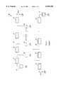
- FIG. 1is a schematic diagram of a known distributed amplifier.
- FIG. 2is a schematic diagram of a distributed amplifier topology with distributed feedback in accordance with the present invention.
- FIG. 3is a graphical illustration of the gain as a function of frequency for a conventional distributed amplifier with no feedback.
- FIG. 4is similar to FIG. 3 but for a distributed amplifier with distributed feedback in accordance with the present invention with a 5.5 dB gain reduction relative to FIG. 3.
- FIG. 5is similar to FIG. 4 but with a 3 dB gain reduction.
- FIG. 6is a graphical illustration of the gain as a function of frequency from 20 MHz to 12 GHz of a distributed amplifier in accordance with the present invention with distributed feedback with a 5.5 dB gain reduction relative to the conventional amplifier with no feedback illustrated in FIG. 3.
- FIG. 7is a graphical illustration of the IP3 performance as a function of frequency for a distributed amplifier with distributed feedback with a 5.5 dB gain reduction.
- FIG. 8is a graphical illustration of the noise figure performance for a distributed amplifier with distributed feedback with a 5.5 dB gain reduction relative to FIG. 3 for a frequency range of 20 MHz to 100 MHz.
- FIG. 9is similar to FIG. 8 but for a frequency range from 20 MHz to 12 GHz.
- the present inventionrelates to a distributed amplifier topology as illustrated in FIG. 2 and identified with the reference numeral 60.
- An important aspect of the inventionrelates to a distributed feedback network which forms a part of the topology which enables the gain of the distributed amplifier to be varied without significantly affecting the noise figure, IP3 and multi-octave frequency performance of the device.
- the distributed amplifier 60obviates the need for segmented dual gate FETS.
- distributed amplifier topology 60may be formed from HEMTs, MESFETS and FETS (herein after referred to as FETS) utilizing relatively less complex and known processing techniques to form a monolithic microwave integrated circuit (MMIC).
- MMICmonolithic microwave integrated circuit
- the distributed amplifier topology 60 in accordance with the present inventionincludes n amplifier stages 62, 64 and 66.
- Each amplifier stage 62, 64 and 66includes a FET, MESFET or HEMT 68, 70, 72.
- Each FET 68, 70, 72is configured in a common source configuration.
- the distributed amplifier topology 60 in accordance with the present inventionis configured such that the gate terminals G of each of the FETS 68, 70 and 72 are connected to a common gate line 74.
- the drain terminals D of each of the FETS 68, 70 and 72are coupled to a common drain line 76.
- the gate line 74 and drain line 76form artificial transmission lines.
- the effective input capacitance for each FET 68, 70 and 72is its respective gate to channel capacitance C GS .
- the effective output capacitance for each FET 68, 70 and 72is its drain to source capacitance C DS .
- the respective input and output capacitances for each stage 62, 64 and 66combined with lumped inductances formed from, for example micro-strip lines 63-73, to form the artificial transmission line 74 and 76.
- Input signalsare applied to a pair of input terminals 78, connected to the gate line 74 and AC ground.
- the output of the distributed amplifier 60is available at a pair of output terminals 80, connected to the drain line 76 and ground.
- a gate line termination impedance 82is connected between the gate line 74 and ground.
- a drain line termination impedance 84is connected between the drain line 76 and AC ground.
- the value of the gate line termination impedance 82is selected to match the characteristic impedance of the gate line 74.
- the value of the drain line termination impedance 84is selected to match the characteristic impedance of the drain line 76. Exemplary values of 50 ⁇ are illustrated in FIG. 2 for both the gate line termination impedance 82 and the drain line termination impedance 84. It is to be understood that other values for the termination impedance 82 and 84 are within the broad scope of the present invention.
- drain bias voltage V DDis applied to the drain line 76, for example by way of a drain bias inductance 86, which may be formed from a microstrip line.
- the value of the drain bias inductance 86is a combination of an on-chip U-strip spiral inductor and off-chip Toroid inductor.
- the inductance value of the on-chip spiralis large enough to reactively block rf-energy in the band of 3 GHz to 20 GHz, while not too large such that its resonant point interferes with circuit operation.
- the off chip toroid valueis chosen such that rf-energy is blocked down to 20 MHz.
- Gate biasingis coupled to the gate terminals G of each of the FETS 68, 70 and 72 and is resistively coupled to a gate bias voltage V GG by way of gate bias resistances 88, 90 and 92, respectively.
- the value of the gate bias resistors 88, 90 and 92is chosen to be larger than the reactance of the dc-block capacitor at 20 Mhz, 106, 108, and 110.
- the purpose of the resistoris to both reduce any rf-energy feeding into the gate of the device through the gate bias network, and reduce leakage of input signal through the bias network.
- each amplifier stage 62, 64 and 66 of the distributed amplifier topology 60includes a common source FET 68, 70 and 72 and a negative feedback network.
- the negative feedback networkenables the gain reduction to be distributed down the transmission lines 74 and 76.
- Each negative feedback networkincludes a source resistor 94, 96, 98, connected between the source terminal of each FETS 68, 70 and 72 and ground; a feedback resistor 100, 102 and 104 coupled between the drain terminal and the gate terminal for each FET 68, 70 and 72; and a gate dc blocking capacitor 106, 108 and 110, connected between the gate terminal and the feedback resistors 100, 102 and 104 for each FET 68, 70 and 72.
- the gate dc blocking capacitors 106, 108 and 110may be formed as distributed capacitors to provide dc blocking between the gate and drain bias voltages.
- the negative feedback networksprovide for wide band gain reduction down the artificial transmission lines 74 and 76 and also improve the stability of the device. Since the negative feedback networks are formed from resistive elements, the gain of the amplifier can be varied (reduced) without affecting the frequency operation of the device 60, since there are no capacitors in the gate-drain feedback path. More particularly, the gain of the device 60 can be varied by varying the values of the feedback resistors 100, 102, 104 and the source resistors 94, 96, 98 down to lower frequencies (10-20 MHz) without affecting the frequency performance of the device. Additional gain reduction at lower frequencies may be achieved through a distributed capacitor divider formed between the capacitors 106, 108 and 110 and the gate to channel capacitance C GS of the FETs 68, 70 and 72.
- FIG. 3represents a graphical illustration of gain as a function of frequency of a conventional distributed amplifier without feedback, such as a TRW Model No. AUH158C.
- the frequency range of the conventional distributed amplifieris about 20 MHz to about 14 GHz.
- FIG. 3illustrates the gain characteristics in the range from 3-20 GHz.
- the gainis relatively flat at about 13.5 dB between 3 and 14 GHz.
- the measured return lossesare 14 dB maximum while the IP3 performance is 28 dbm and the noise figure is 3 dbm maximum.
- FIGS. 4 and 5illustrate the performance characteristics of a distributed amplifier topology 60 in accordance with the present invention for different gain characteristics.
- FIG. 4illustrates a 5.5 dB gain reduction relative to the distributed amplifier without feedback illustrated in FIG. 3.
- the distributed amplifier characteristics illustrated in FIG. 3can be considered as a distributed amplifier topology in accordance with the present invention with infinite values for a feedback resistors 100, 102 and 104 while the source resistors 94, 96 and 98 are short circuited.
- values of 1.6 K ⁇ for the feedback resistors 100, 102 and 104are selected while exemplary values of 15 ⁇ for the resistors 94, 96 and 98.
- FIG. 5illustrates a 3 dB gain reduction relative to FIG. 3 with an exemplary values of 1.8 K ⁇ for the feedback resistors 100, 102 and 104 and exemplary values of 7.5 ⁇ for the source resistors 94, 96 and 98.
- FIGS. 6-9illustrate the gain, IP3 and noise figure performance of the distributed amplifier with 5.5 dB gain reduction relative to FIG. 3.
- the gain characteristic between 3 and 16 GHzis about 8.5 dB, which represents a 5.5 dB gain reduction relative to FIG. 2.
- the return loss, IP3 and noise figure performance of a distributed amplifier in accordance with the present inventionis similar to the return loss, IP3 and noise figure performance of the distributed amplifier without feedback illustrated in FIG. 3. More particularly, the return loss performance for a distributed amplifier in accordance with the present invention with a 5.5 dB gain reduction relative to FIG. 3 is about 12 dB while the IP performance is about 28 dBm. Over the operating range of the distributed amplifier, 20 MHz-16 GHz, the noise figure performance is about 4.5 dB.
- FIG. 5illustrates a distributed amplifier in accordance with the present invention with a 3 dB gain reduction relative to FIG. 3. As shown, over the frequency range from 3 to 16 GHz, the gain is about 10.5 dB while the return losses are 12 dB, the IP3 performance is 30 dBm and the noise figure is 4.5 dB.
- the distributed amplifier topology in accordance with the present inventionenables the gain characteristic to be varied independent of the frequency response while having little affect on the IP3, return loss and noise figure performance.
- the distributed amplifier topologyis amenable to conventional circuit processing techniques to form a microwave monolithic integrated circuit. Gain characteristics of the distributed amplifier are changed by merely changing the values of the feedback resistors 100, 102 and 104 as well as the source resistors 94, 96 and 98 to enable distributed amplifiers with various gain characteristics to be rather easily fabricated.
Landscapes
- Engineering & Computer Science (AREA)
- Power Engineering (AREA)
- Microwave Amplifiers (AREA)
Abstract
Description
Claims (7)
Priority Applications (1)
| Application Number | Priority Date | Filing Date | Title |
|---|---|---|---|
| US09/054,934US6049250A (en) | 1998-04-03 | 1998-04-03 | Dittributed feed back distributed amplifier |
Applications Claiming Priority (1)
| Application Number | Priority Date | Filing Date | Title |
|---|---|---|---|
| US09/054,934US6049250A (en) | 1998-04-03 | 1998-04-03 | Dittributed feed back distributed amplifier |
Publications (1)
| Publication Number | Publication Date |
|---|---|
| US6049250Atrue US6049250A (en) | 2000-04-11 |
Family
ID=21994481
Family Applications (1)
| Application Number | Title | Priority Date | Filing Date |
|---|---|---|---|
| US09/054,934Expired - LifetimeUS6049250A (en) | 1998-04-03 | 1998-04-03 | Dittributed feed back distributed amplifier |
Country Status (1)
| Country | Link |
|---|---|
| US (1) | US6049250A (en) |
Cited By (45)
| Publication number | Priority date | Publication date | Assignee | Title |
|---|---|---|---|---|
| US6342815B1 (en)* | 2000-10-04 | 2002-01-29 | Trw Inc. | Manufacturable HBT power distributed amplifier for wideband telecommunications |
| US6377125B1 (en)* | 2001-03-15 | 2002-04-23 | Motorola.Inc. | Distributed amplifier having separately biased sections |
| US6400226B2 (en)* | 1999-12-02 | 2002-06-04 | Fujitsu Limited | Distributed amplifier with improved flatness of frequency characteristic |
| US20030006846A1 (en)* | 2001-06-28 | 2003-01-09 | Alcatel | Broad-band biasing system for biasing an electronic circuit and an amplifier incorporating the system |
| US6566956B2 (en)* | 2000-07-14 | 2003-05-20 | Hitachi, Ltd. | High frequency power amplifier |
| US6597243B1 (en)* | 2001-12-31 | 2003-07-22 | Agere Systems, Inc. | Distributed amplifier having a tapered transconductance architecture |
| US20030184383A1 (en)* | 2002-03-29 | 2003-10-02 | Yasunori Ogawa | Distributed amplifier |
| US6650185B1 (en)* | 2002-04-26 | 2003-11-18 | Motorola, Inc | Frequency selective distributed amplifier |
| US20040070455A1 (en)* | 2002-10-11 | 2004-04-15 | Hong John H. | Wideband, variable-bandwidth distributed amplifier |
| US6727762B1 (en) | 2002-11-26 | 2004-04-27 | Sirenza Microdevices, Inc. | Direct coupled distributed amplifier |
| US6737933B2 (en)* | 2002-01-15 | 2004-05-18 | Nokia Corporation | Circuit topology for attenuator and switch circuits |
| EP1447906A3 (en)* | 2003-02-12 | 2004-11-17 | Northrop Grumman Corporation | Dual gate low noise amplifier |
| US20050014471A1 (en)* | 2003-07-15 | 2005-01-20 | Lockheed Martin Corporation | Method and apparatus for transmission and reception of signals |
| US20050248407A1 (en)* | 2004-04-29 | 2005-11-10 | Infineon Technologies Ag | Traveling wave amplifier |
| US20070216485A1 (en)* | 2006-03-17 | 2007-09-20 | Kohei Fujii | Linear variable gain traveling wave amplifier |
| US20080143443A1 (en)* | 2005-04-07 | 2008-06-19 | Analog Devices, Inc. | Vector modulator having attenuators with continuous input steering |
| US20090212869A1 (en)* | 2008-02-22 | 2009-08-27 | Endwave Corporation | Distributed amplifier with negative feedback |
| JP2009538051A (en)* | 2006-05-18 | 2009-10-29 | ザ リージェンツ オブ ザ ユニバーシティ オブ カリフォルニア | Power combiner using metamaterial right-handed / left-handed composite transmission line at infinite wavelength frequency |
| WO2009139814A3 (en)* | 2008-04-17 | 2010-01-14 | Hittite Microwave Corporation | Modified distributed amplifier to improve low frequency efficiency and noise figure |
| US20100033252A1 (en)* | 2008-08-05 | 2010-02-11 | Northrop Grumman Systems Corporation | Method and apparatus for josephson distributed output amplifier |
| US8451059B1 (en) | 2009-01-02 | 2013-05-28 | Rf Micro Devices, Inc. | Capacitively-coupled distributed amplifier with baseband performance |
| US8665022B2 (en) | 2011-04-28 | 2014-03-04 | Rf Micro Devices, Inc. | Low noise-linear power distributed amplifier |
| US8823455B2 (en) | 2011-09-13 | 2014-09-02 | Rf Micro Devices, Inc. | Matrix distributed power amplifier |
| US8988097B2 (en) | 2012-08-24 | 2015-03-24 | Rf Micro Devices, Inc. | Method for on-wafer high voltage testing of semiconductor devices |
| US9070761B2 (en) | 2012-08-27 | 2015-06-30 | Rf Micro Devices, Inc. | Field effect transistor (FET) having fingers with rippled edges |
| US9093420B2 (en) | 2012-04-18 | 2015-07-28 | Rf Micro Devices, Inc. | Methods for fabricating high voltage field effect transistor finger terminations |
| US9124221B2 (en) | 2012-07-16 | 2015-09-01 | Rf Micro Devices, Inc. | Wide bandwidth radio frequency amplier having dual gate transistors |
| US9129802B2 (en) | 2012-08-27 | 2015-09-08 | Rf Micro Devices, Inc. | Lateral semiconductor device with vertical breakdown region |
| US9142620B2 (en) | 2012-08-24 | 2015-09-22 | Rf Micro Devices, Inc. | Power device packaging having backmetals couple the plurality of bond pads to the die backside |
| US9147632B2 (en) | 2012-08-24 | 2015-09-29 | Rf Micro Devices, Inc. | Semiconductor device having improved heat dissipation |
| US9202874B2 (en) | 2012-08-24 | 2015-12-01 | Rf Micro Devices, Inc. | Gallium nitride (GaN) device with leakage current-based over-voltage protection |
| US9325281B2 (en) | 2012-10-30 | 2016-04-26 | Rf Micro Devices, Inc. | Power amplifier controller |
| US9425752B2 (en) | 2011-03-09 | 2016-08-23 | Hittite Microwave Llc | Distributed amplifier with improved stabilization |
| US9455327B2 (en) | 2014-06-06 | 2016-09-27 | Qorvo Us, Inc. | Schottky gated transistor with interfacial layer |
| US9536803B2 (en) | 2014-09-05 | 2017-01-03 | Qorvo Us, Inc. | Integrated power module with improved isolation and thermal conductivity |
| US9673759B1 (en) | 2015-12-21 | 2017-06-06 | Raytheon Company | Off-chip distributed drain biasing of high power distributed amplifier monolithic microwave integrated circuit (MMIC) chips |
| US9825603B2 (en) | 2015-10-05 | 2017-11-21 | Qorvo Us, Inc. | Active drain terminated distributed amplifier |
| US9917080B2 (en) | 2012-08-24 | 2018-03-13 | Qorvo US. Inc. | Semiconductor device with electrical overstress (EOS) protection |
| US10014826B2 (en) | 2015-12-10 | 2018-07-03 | Analog Devices, Inc. | Apparatus and methods for power enhancement of self-biased distributed amplifiers with gate bias networks |
| US10062684B2 (en) | 2015-02-04 | 2018-08-28 | Qorvo Us, Inc. | Transition frequency multiplier semiconductor device |
| US10340858B2 (en) | 2016-07-12 | 2019-07-02 | Qorvo Us, Inc. | Linearized distributed amplifier architecture |
| US10615158B2 (en) | 2015-02-04 | 2020-04-07 | Qorvo Us, Inc. | Transition frequency multiplier semiconductor device |
| CN112865725A (en)* | 2021-01-13 | 2021-05-28 | 中电国基南方集团有限公司 | Ultra-wideband high-power high-efficiency monolithic integrated power amplifier circuit structure |
| US11139790B2 (en) | 2019-11-14 | 2021-10-05 | Industrial Technology Research Institute | Distributed amplifier with low supply voltage and low power consumption for full-chip high-speed communication |
| JP7625154B1 (en) | 2024-04-24 | 2025-01-31 | 三菱電機株式会社 | Distributed Amplifier |
Citations (13)
| Publication number | Priority date | Publication date | Assignee | Title |
|---|---|---|---|---|
| US3222611A (en)* | 1962-03-01 | 1965-12-07 | Jr Charles W Norton | Distributed amplifier |
| US4103245A (en)* | 1975-08-29 | 1978-07-25 | Nippon Gakki Seizo Kabushiki Kaisha | Transistor amplifier for low level signal |
| US4631493A (en)* | 1985-03-18 | 1986-12-23 | Eaton Corporation | Circuit for DC biasing |
| US4918401A (en)* | 1985-09-30 | 1990-04-17 | Siemens Aktiengesellschaft | Step adjustable distributed amplifier network structure |
| US4947136A (en)* | 1989-09-18 | 1990-08-07 | General Electric Company | Variable gain distributed amplifier |
| US5208547A (en)* | 1991-06-06 | 1993-05-04 | Raytheon Company | Distributed amplifier having negative feedback |
| US5274339A (en)* | 1992-08-27 | 1993-12-28 | Raytheon Company | Gain compensation circuit |
| US5386130A (en)* | 1992-11-04 | 1995-01-31 | U.S. Philips Corporation | Semiconductor device comprising a broadband and high-gain monolithic integrated circuit for a distributed amplifier |
| US5412347A (en)* | 1992-12-03 | 1995-05-02 | U.S. Philips Corporation | Compact cascadable microwave amplifier circuits |
| US5414387A (en)* | 1993-07-14 | 1995-05-09 | Mitsubishi Denki Kabushiki Kaisha | Distributed amplifier and bidirectional amplifier |
| US5559472A (en)* | 1995-05-02 | 1996-09-24 | Trw Inc. | Loss compensated gain cell for distributed amplifiers |
| US5694085A (en)* | 1996-02-14 | 1997-12-02 | Glenayre Electronics, Inc. | High-power amplifier using parallel transistors |
| US5751190A (en)* | 1996-08-22 | 1998-05-12 | Northern Telecom Limited | Gain-controlled amplifier and distributed amplifier |
- 1998
- 1998-04-03USUS09/054,934patent/US6049250A/ennot_activeExpired - Lifetime
Patent Citations (13)
| Publication number | Priority date | Publication date | Assignee | Title |
|---|---|---|---|---|
| US3222611A (en)* | 1962-03-01 | 1965-12-07 | Jr Charles W Norton | Distributed amplifier |
| US4103245A (en)* | 1975-08-29 | 1978-07-25 | Nippon Gakki Seizo Kabushiki Kaisha | Transistor amplifier for low level signal |
| US4631493A (en)* | 1985-03-18 | 1986-12-23 | Eaton Corporation | Circuit for DC biasing |
| US4918401A (en)* | 1985-09-30 | 1990-04-17 | Siemens Aktiengesellschaft | Step adjustable distributed amplifier network structure |
| US4947136A (en)* | 1989-09-18 | 1990-08-07 | General Electric Company | Variable gain distributed amplifier |
| US5208547A (en)* | 1991-06-06 | 1993-05-04 | Raytheon Company | Distributed amplifier having negative feedback |
| US5274339A (en)* | 1992-08-27 | 1993-12-28 | Raytheon Company | Gain compensation circuit |
| US5386130A (en)* | 1992-11-04 | 1995-01-31 | U.S. Philips Corporation | Semiconductor device comprising a broadband and high-gain monolithic integrated circuit for a distributed amplifier |
| US5412347A (en)* | 1992-12-03 | 1995-05-02 | U.S. Philips Corporation | Compact cascadable microwave amplifier circuits |
| US5414387A (en)* | 1993-07-14 | 1995-05-09 | Mitsubishi Denki Kabushiki Kaisha | Distributed amplifier and bidirectional amplifier |
| US5559472A (en)* | 1995-05-02 | 1996-09-24 | Trw Inc. | Loss compensated gain cell for distributed amplifiers |
| US5694085A (en)* | 1996-02-14 | 1997-12-02 | Glenayre Electronics, Inc. | High-power amplifier using parallel transistors |
| US5751190A (en)* | 1996-08-22 | 1998-05-12 | Northern Telecom Limited | Gain-controlled amplifier and distributed amplifier |
Non-Patent Citations (4)
| Title |
|---|
| "Mesfet Distributed Amplifier Design Guidelines"; by Beyer, et al., IEEE Transactions on Microwave Theory and Techniques, vol. MTT-32, No. 3, Mar. 1984, pp. 268-275. |
| "On Gain-Bandwidth Product for Distributed Amplifiers"; by Becker, et al., IEEE Transactions on Microwave Theory and Techniques, vol. MTT-34, No. 6, Jun. 1986, pp. 736-738. |
| Mesfet Distributed Amplifier Design Guidelines ; by Beyer, et al., IEEE Transactions on Microwave Theory and Techniques, vol. MTT 32, No. 3, Mar. 1984, pp. 268 275.* |
| On Gain Bandwidth Product for Distributed Amplifiers ; by Becker, et al., IEEE Transactions on Microwave Theory and Techniques, vol. MTT 34, No. 6, Jun. 1986, pp. 736 738.* |
Cited By (63)
| Publication number | Priority date | Publication date | Assignee | Title |
|---|---|---|---|---|
| US6400226B2 (en)* | 1999-12-02 | 2002-06-04 | Fujitsu Limited | Distributed amplifier with improved flatness of frequency characteristic |
| US6566956B2 (en)* | 2000-07-14 | 2003-05-20 | Hitachi, Ltd. | High frequency power amplifier |
| US6342815B1 (en)* | 2000-10-04 | 2002-01-29 | Trw Inc. | Manufacturable HBT power distributed amplifier for wideband telecommunications |
| US6377125B1 (en)* | 2001-03-15 | 2002-04-23 | Motorola.Inc. | Distributed amplifier having separately biased sections |
| US20030006846A1 (en)* | 2001-06-28 | 2003-01-09 | Alcatel | Broad-band biasing system for biasing an electronic circuit and an amplifier incorporating the system |
| US6788149B2 (en)* | 2001-06-28 | 2004-09-07 | Avanex Corporation | Broad-band biasing system for biasing an electronic circuit and an amplifier incorporating the system |
| US6597243B1 (en)* | 2001-12-31 | 2003-07-22 | Agere Systems, Inc. | Distributed amplifier having a tapered transconductance architecture |
| US6737933B2 (en)* | 2002-01-15 | 2004-05-18 | Nokia Corporation | Circuit topology for attenuator and switch circuits |
| US6778015B2 (en)* | 2002-03-29 | 2004-08-17 | Oki Electric Industry Co., Ltd. | Distributed amplifier |
| US20030184383A1 (en)* | 2002-03-29 | 2003-10-02 | Yasunori Ogawa | Distributed amplifier |
| US6650185B1 (en)* | 2002-04-26 | 2003-11-18 | Motorola, Inc | Frequency selective distributed amplifier |
| US20040070455A1 (en)* | 2002-10-11 | 2004-04-15 | Hong John H. | Wideband, variable-bandwidth distributed amplifier |
| US6768380B2 (en) | 2002-10-11 | 2004-07-27 | Caldera Micro Technology, Inc. | Wideband, variable-bandwidth distributed amplifier |
| US6727762B1 (en) | 2002-11-26 | 2004-04-27 | Sirenza Microdevices, Inc. | Direct coupled distributed amplifier |
| EP1447906A3 (en)* | 2003-02-12 | 2004-11-17 | Northrop Grumman Corporation | Dual gate low noise amplifier |
| US20050014471A1 (en)* | 2003-07-15 | 2005-01-20 | Lockheed Martin Corporation | Method and apparatus for transmission and reception of signals |
| US8107893B2 (en)* | 2003-07-15 | 2012-01-31 | Lockheed Martin Corporation | Method and apparatus for transmission and reception of signals |
| US20050248407A1 (en)* | 2004-04-29 | 2005-11-10 | Infineon Technologies Ag | Traveling wave amplifier |
| DE102004021155B3 (en)* | 2004-04-29 | 2005-12-29 | Infineon Technologies Ag | Traveling wave amplifier |
| US7271657B2 (en) | 2004-04-29 | 2007-09-18 | Infineon Technologies Ag | Traveling wave amplifier |
| US7915956B2 (en)* | 2005-04-07 | 2011-03-29 | Analog Devices, Inc. | Vector modulator having attenuators with continuous input steering |
| US8497735B2 (en) | 2005-04-07 | 2013-07-30 | Analog Devices, Inc. | Vector modulator having attenuators with continuous input steering |
| US20080143443A1 (en)* | 2005-04-07 | 2008-06-19 | Analog Devices, Inc. | Vector modulator having attenuators with continuous input steering |
| US7400200B2 (en)* | 2006-03-17 | 2008-07-15 | Avago Technologies Wireless Ip Pte Ltd | Linear variable gain traveling wave amplifier |
| US20070216485A1 (en)* | 2006-03-17 | 2007-09-20 | Kohei Fujii | Linear variable gain traveling wave amplifier |
| JP2009538051A (en)* | 2006-05-18 | 2009-10-29 | ザ リージェンツ オブ ザ ユニバーシティ オブ カリフォルニア | Power combiner using metamaterial right-handed / left-handed composite transmission line at infinite wavelength frequency |
| US7804362B2 (en) | 2008-02-22 | 2010-09-28 | Microsemi Corporation | Distributed amplifier with negative feedback |
| US20090212869A1 (en)* | 2008-02-22 | 2009-08-27 | Endwave Corporation | Distributed amplifier with negative feedback |
| US20100019851A1 (en)* | 2008-04-17 | 2010-01-28 | Keith Benson | Modified distributed amplifier to improve low frequency efficiency and noise figure |
| US7843268B2 (en) | 2008-04-17 | 2010-11-30 | Hittite Microwave Corporation | Modified distributed amplifier to improve low frequency efficiency and noise figure |
| WO2009139814A3 (en)* | 2008-04-17 | 2010-01-14 | Hittite Microwave Corporation | Modified distributed amplifier to improve low frequency efficiency and noise figure |
| US7724083B2 (en)* | 2008-08-05 | 2010-05-25 | Northrop Grumman Systems Corporation | Method and apparatus for Josephson distributed output amplifier |
| US20100033252A1 (en)* | 2008-08-05 | 2010-02-11 | Northrop Grumman Systems Corporation | Method and apparatus for josephson distributed output amplifier |
| US8451059B1 (en) | 2009-01-02 | 2013-05-28 | Rf Micro Devices, Inc. | Capacitively-coupled distributed amplifier with baseband performance |
| US10164579B2 (en) | 2011-03-09 | 2018-12-25 | Hittite Microwave Llc | Distributed amplifier |
| US10122325B2 (en) | 2011-03-09 | 2018-11-06 | Hittite Microwave Llc | Distributed amplifier with improved stabilization |
| US9425752B2 (en) | 2011-03-09 | 2016-08-23 | Hittite Microwave Llc | Distributed amplifier with improved stabilization |
| US8665022B2 (en) | 2011-04-28 | 2014-03-04 | Rf Micro Devices, Inc. | Low noise-linear power distributed amplifier |
| US8823455B2 (en) | 2011-09-13 | 2014-09-02 | Rf Micro Devices, Inc. | Matrix distributed power amplifier |
| US9136341B2 (en) | 2012-04-18 | 2015-09-15 | Rf Micro Devices, Inc. | High voltage field effect transistor finger terminations |
| US9093420B2 (en) | 2012-04-18 | 2015-07-28 | Rf Micro Devices, Inc. | Methods for fabricating high voltage field effect transistor finger terminations |
| US9564497B2 (en) | 2012-04-18 | 2017-02-07 | Qorvo Us, Inc. | High voltage field effect transitor finger terminations |
| US9124221B2 (en) | 2012-07-16 | 2015-09-01 | Rf Micro Devices, Inc. | Wide bandwidth radio frequency amplier having dual gate transistors |
| US9917080B2 (en) | 2012-08-24 | 2018-03-13 | Qorvo US. Inc. | Semiconductor device with electrical overstress (EOS) protection |
| US9142620B2 (en) | 2012-08-24 | 2015-09-22 | Rf Micro Devices, Inc. | Power device packaging having backmetals couple the plurality of bond pads to the die backside |
| US9147632B2 (en) | 2012-08-24 | 2015-09-29 | Rf Micro Devices, Inc. | Semiconductor device having improved heat dissipation |
| US9202874B2 (en) | 2012-08-24 | 2015-12-01 | Rf Micro Devices, Inc. | Gallium nitride (GaN) device with leakage current-based over-voltage protection |
| US8988097B2 (en) | 2012-08-24 | 2015-03-24 | Rf Micro Devices, Inc. | Method for on-wafer high voltage testing of semiconductor devices |
| US9640632B2 (en) | 2012-08-24 | 2017-05-02 | Qorvo Us, Inc. | Semiconductor device having improved heat dissipation |
| US9129802B2 (en) | 2012-08-27 | 2015-09-08 | Rf Micro Devices, Inc. | Lateral semiconductor device with vertical breakdown region |
| US9070761B2 (en) | 2012-08-27 | 2015-06-30 | Rf Micro Devices, Inc. | Field effect transistor (FET) having fingers with rippled edges |
| US9325281B2 (en) | 2012-10-30 | 2016-04-26 | Rf Micro Devices, Inc. | Power amplifier controller |
| US9455327B2 (en) | 2014-06-06 | 2016-09-27 | Qorvo Us, Inc. | Schottky gated transistor with interfacial layer |
| US9536803B2 (en) | 2014-09-05 | 2017-01-03 | Qorvo Us, Inc. | Integrated power module with improved isolation and thermal conductivity |
| US10062684B2 (en) | 2015-02-04 | 2018-08-28 | Qorvo Us, Inc. | Transition frequency multiplier semiconductor device |
| US10615158B2 (en) | 2015-02-04 | 2020-04-07 | Qorvo Us, Inc. | Transition frequency multiplier semiconductor device |
| US9825603B2 (en) | 2015-10-05 | 2017-11-21 | Qorvo Us, Inc. | Active drain terminated distributed amplifier |
| US10014826B2 (en) | 2015-12-10 | 2018-07-03 | Analog Devices, Inc. | Apparatus and methods for power enhancement of self-biased distributed amplifiers with gate bias networks |
| US9673759B1 (en) | 2015-12-21 | 2017-06-06 | Raytheon Company | Off-chip distributed drain biasing of high power distributed amplifier monolithic microwave integrated circuit (MMIC) chips |
| US10340858B2 (en) | 2016-07-12 | 2019-07-02 | Qorvo Us, Inc. | Linearized distributed amplifier architecture |
| US11139790B2 (en) | 2019-11-14 | 2021-10-05 | Industrial Technology Research Institute | Distributed amplifier with low supply voltage and low power consumption for full-chip high-speed communication |
| CN112865725A (en)* | 2021-01-13 | 2021-05-28 | 中电国基南方集团有限公司 | Ultra-wideband high-power high-efficiency monolithic integrated power amplifier circuit structure |
| JP7625154B1 (en) | 2024-04-24 | 2025-01-31 | 三菱電機株式会社 | Distributed Amplifier |
Similar Documents
| Publication | Publication Date | Title |
|---|---|---|
| US6049250A (en) | Dittributed feed back distributed amplifier | |
| US4788511A (en) | Distributed power amplifier | |
| US4975604A (en) | Automatic return-loss optimization of a variable fet attenuator | |
| US6472941B2 (en) | Distributed amplifier with terminating circuit capable of improving gain flatness at low frequencies | |
| US4540954A (en) | Singly terminated distributed amplifier | |
| US5208547A (en) | Distributed amplifier having negative feedback | |
| US5986518A (en) | Distributed MMIC active quadrature hybrid and method for providing in-phase and quadrature-phase signals | |
| US20160134244A1 (en) | High-frequency amplifier | |
| US7245186B2 (en) | Bandpass amplifier | |
| US4967169A (en) | FET monolithic microwave integrated circuit variable slope gain-equalizer | |
| US5012203A (en) | Distributed amplifier with attenuation compensation | |
| US6630861B2 (en) | Variable gain amplifier | |
| US5072199A (en) | Broadband N-way active power splitter | |
| JP2000124709A (en) | Microwave variable attenuation circuit | |
| KR930011384B1 (en) | Microwave integrated circuits | |
| US5099155A (en) | Active element filter network | |
| JPH0575357A (en) | Low noise amplifier | |
| US5017887A (en) | High frequency IC power amplifier | |
| JP3886642B2 (en) | High frequency gain variable amplifier circuit | |
| JP2841724B2 (en) | Semiconductor device | |
| KR100375678B1 (en) | Matrix distributed amplifier having higher gain-bandwith-product | |
| JPH08321726A (en) | Amplifier circuit | |
| JP3150806B2 (en) | Microwave filter circuit | |
| JPH01188007A (en) | Negative feedback amplifier circuit | |
| Maeda et al. | Microwave variable-gain amplifier with dual-gate GaAs FET |
Legal Events
| Date | Code | Title | Description |
|---|---|---|---|
| AS | Assignment | Owner name:TRW INC., CALIFORNIA Free format text:ASSIGNMENT OF ASSIGNORS INTEREST;ASSIGNORS:KINTIS, MARK;TOMASEVIC, PETAR;REEL/FRAME:009176/0484 Effective date:19980401 | |
| STCF | Information on status: patent grant | Free format text:PATENTED CASE | |
| FEPP | Fee payment procedure | Free format text:PAYOR NUMBER ASSIGNED (ORIGINAL EVENT CODE: ASPN); ENTITY STATUS OF PATENT OWNER: LARGE ENTITY | |
| AS | Assignment | Owner name:NORTHROP GRUMMAN CORPORATION, CALIFORNIA Free format text:ASSIGNMENT OF ASSIGNORS INTEREST;ASSIGNOR:TRW, INC. N/K/A NORTHROP GRUMMAN SPACE AND MISSION SYSTEMS CORPORATION, AN OHIO CORPORATION;REEL/FRAME:013751/0849 Effective date:20030122 Owner name:NORTHROP GRUMMAN CORPORATION,CALIFORNIA Free format text:ASSIGNMENT OF ASSIGNORS INTEREST;ASSIGNOR:TRW, INC. N/K/A NORTHROP GRUMMAN SPACE AND MISSION SYSTEMS CORPORATION, AN OHIO CORPORATION;REEL/FRAME:013751/0849 Effective date:20030122 | |
| FPAY | Fee payment | Year of fee payment:4 | |
| FPAY | Fee payment | Year of fee payment:8 | |
| REMI | Maintenance fee reminder mailed | ||
| FEPP | Fee payment procedure | Free format text:PAYER NUMBER DE-ASSIGNED (ORIGINAL EVENT CODE: RMPN); ENTITY STATUS OF PATENT OWNER: LARGE ENTITY Free format text:PAYOR NUMBER ASSIGNED (ORIGINAL EVENT CODE: ASPN); ENTITY STATUS OF PATENT OWNER: LARGE ENTITY | |
| AS | Assignment | Owner name:NORTHROP GRUMMAN SPACE & MISSION SYSTEMS CORP.,CAL Free format text:ASSIGNMENT OF ASSIGNORS INTEREST;ASSIGNOR:NORTHROP GRUMMAN CORPORTION;REEL/FRAME:023699/0551 Effective date:20091125 Owner name:NORTHROP GRUMMAN SPACE & MISSION SYSTEMS CORP., CA Free format text:ASSIGNMENT OF ASSIGNORS INTEREST;ASSIGNOR:NORTHROP GRUMMAN CORPORTION;REEL/FRAME:023699/0551 Effective date:20091125 | |
| AS | Assignment | Owner name:NORTHROP GRUMMAN SYSTEMS CORPORATION,CALIFORNIA Free format text:ASSIGNMENT OF ASSIGNORS INTEREST;ASSIGNOR:NORTHROP GRUMMAN SPACE & MISSION SYSTEMS CORP.;REEL/FRAME:023915/0446 Effective date:20091210 Owner name:NORTHROP GRUMMAN SYSTEMS CORPORATION, CALIFORNIA Free format text:ASSIGNMENT OF ASSIGNORS INTEREST;ASSIGNOR:NORTHROP GRUMMAN SPACE & MISSION SYSTEMS CORP.;REEL/FRAME:023915/0446 Effective date:20091210 | |
| FPAY | Fee payment | Year of fee payment:12 |