US6049124A - Semiconductor package - Google Patents
Semiconductor packageDownload PDFInfo
- Publication number
- US6049124A US6049124AUS08/988,231US98823197AUS6049124AUS 6049124 AUS6049124 AUS 6049124AUS 98823197 AUS98823197 AUS 98823197AUS 6049124 AUS6049124 AUS 6049124A
- Authority
- US
- United States
- Prior art keywords
- semiconductor chip
- package substrate
- semiconductor
- package
- thermal expansion
- Prior art date
- Legal status (The legal status is an assumption and is not a legal conclusion. Google has not performed a legal analysis and makes no representation as to the accuracy of the status listed.)
- Expired - Lifetime
Links
Images


Classifications
- H—ELECTRICITY
- H01—ELECTRIC ELEMENTS
- H01L—SEMICONDUCTOR DEVICES NOT COVERED BY CLASS H10
- H01L24/00—Arrangements for connecting or disconnecting semiconductor or solid-state bodies; Methods or apparatus related thereto
- H01L24/01—Means for bonding being attached to, or being formed on, the surface to be connected, e.g. chip-to-package, die-attach, "first-level" interconnects; Manufacturing methods related thereto
- H01L24/26—Layer connectors, e.g. plate connectors, solder or adhesive layers; Manufacturing methods related thereto
- H01L24/31—Structure, shape, material or disposition of the layer connectors after the connecting process
- H01L24/32—Structure, shape, material or disposition of the layer connectors after the connecting process of an individual layer connector
- H—ELECTRICITY
- H01—ELECTRIC ELEMENTS
- H01L—SEMICONDUCTOR DEVICES NOT COVERED BY CLASS H10
- H01L21/00—Processes or apparatus adapted for the manufacture or treatment of semiconductor or solid state devices or of parts thereof
- H01L21/02—Manufacture or treatment of semiconductor devices or of parts thereof
- H01L21/04—Manufacture or treatment of semiconductor devices or of parts thereof the devices having potential barriers, e.g. a PN junction, depletion layer or carrier concentration layer
- H01L21/50—Assembly of semiconductor devices using processes or apparatus not provided for in a single one of the groups H01L21/18 - H01L21/326 or H10D48/04 - H10D48/07 e.g. sealing of a cap to a base of a container
- H01L21/56—Encapsulations, e.g. encapsulation layers, coatings
- H01L21/563—Encapsulation of active face of flip-chip device, e.g. underfilling or underencapsulation of flip-chip, encapsulation preform on chip or mounting substrate
- H—ELECTRICITY
- H01—ELECTRIC ELEMENTS
- H01L—SEMICONDUCTOR DEVICES NOT COVERED BY CLASS H10
- H01L24/00—Arrangements for connecting or disconnecting semiconductor or solid-state bodies; Methods or apparatus related thereto
- H01L24/01—Means for bonding being attached to, or being formed on, the surface to be connected, e.g. chip-to-package, die-attach, "first-level" interconnects; Manufacturing methods related thereto
- H01L24/26—Layer connectors, e.g. plate connectors, solder or adhesive layers; Manufacturing methods related thereto
- H01L24/28—Structure, shape, material or disposition of the layer connectors prior to the connecting process
- H01L24/29—Structure, shape, material or disposition of the layer connectors prior to the connecting process of an individual layer connector
- H—ELECTRICITY
- H10—SEMICONDUCTOR DEVICES; ELECTRIC SOLID-STATE DEVICES NOT OTHERWISE PROVIDED FOR
- H10D—INORGANIC ELECTRIC SEMICONDUCTOR DEVICES
- H10D62/00—Semiconductor bodies, or regions thereof, of devices having potential barriers
- H10D62/10—Shapes, relative sizes or dispositions of the regions of the semiconductor bodies; Shapes of the semiconductor bodies
- H10D62/117—Shapes of semiconductor bodies
- H—ELECTRICITY
- H01—ELECTRIC ELEMENTS
- H01L—SEMICONDUCTOR DEVICES NOT COVERED BY CLASS H10
- H01L2224/00—Indexing scheme for arrangements for connecting or disconnecting semiconductor or solid-state bodies and methods related thereto as covered by H01L24/00
- H01L2224/01—Means for bonding being attached to, or being formed on, the surface to be connected, e.g. chip-to-package, die-attach, "first-level" interconnects; Manufacturing methods related thereto
- H01L2224/10—Bump connectors; Manufacturing methods related thereto
- H01L2224/15—Structure, shape, material or disposition of the bump connectors after the connecting process
- H01L2224/16—Structure, shape, material or disposition of the bump connectors after the connecting process of an individual bump connector
- H01L2224/161—Disposition
- H01L2224/16151—Disposition the bump connector connecting between a semiconductor or solid-state body and an item not being a semiconductor or solid-state body, e.g. chip-to-substrate, chip-to-passive
- H01L2224/16221—Disposition the bump connector connecting between a semiconductor or solid-state body and an item not being a semiconductor or solid-state body, e.g. chip-to-substrate, chip-to-passive the body and the item being stacked
- H01L2224/16225—Disposition the bump connector connecting between a semiconductor or solid-state body and an item not being a semiconductor or solid-state body, e.g. chip-to-substrate, chip-to-passive the body and the item being stacked the item being non-metallic, e.g. insulating substrate with or without metallisation
- H—ELECTRICITY
- H01—ELECTRIC ELEMENTS
- H01L—SEMICONDUCTOR DEVICES NOT COVERED BY CLASS H10
- H01L2224/00—Indexing scheme for arrangements for connecting or disconnecting semiconductor or solid-state bodies and methods related thereto as covered by H01L24/00
- H01L2224/01—Means for bonding being attached to, or being formed on, the surface to be connected, e.g. chip-to-package, die-attach, "first-level" interconnects; Manufacturing methods related thereto
- H01L2224/26—Layer connectors, e.g. plate connectors, solder or adhesive layers; Manufacturing methods related thereto
- H01L2224/31—Structure, shape, material or disposition of the layer connectors after the connecting process
- H01L2224/32—Structure, shape, material or disposition of the layer connectors after the connecting process of an individual layer connector
- H01L2224/321—Disposition
- H01L2224/32151—Disposition the layer connector connecting between a semiconductor or solid-state body and an item not being a semiconductor or solid-state body, e.g. chip-to-substrate, chip-to-passive
- H01L2224/32221—Disposition the layer connector connecting between a semiconductor or solid-state body and an item not being a semiconductor or solid-state body, e.g. chip-to-substrate, chip-to-passive the body and the item being stacked
- H01L2224/32225—Disposition the layer connector connecting between a semiconductor or solid-state body and an item not being a semiconductor or solid-state body, e.g. chip-to-substrate, chip-to-passive the body and the item being stacked the item being non-metallic, e.g. insulating substrate with or without metallisation
- H—ELECTRICITY
- H01—ELECTRIC ELEMENTS
- H01L—SEMICONDUCTOR DEVICES NOT COVERED BY CLASS H10
- H01L2224/00—Indexing scheme for arrangements for connecting or disconnecting semiconductor or solid-state bodies and methods related thereto as covered by H01L24/00
- H01L2224/73—Means for bonding being of different types provided for in two or more of groups H01L2224/10, H01L2224/18, H01L2224/26, H01L2224/34, H01L2224/42, H01L2224/50, H01L2224/63, H01L2224/71
- H01L2224/732—Location after the connecting process
- H01L2224/73201—Location after the connecting process on the same surface
- H01L2224/73203—Bump and layer connectors
- H01L2224/73204—Bump and layer connectors the bump connector being embedded into the layer connector
- H—ELECTRICITY
- H01—ELECTRIC ELEMENTS
- H01L—SEMICONDUCTOR DEVICES NOT COVERED BY CLASS H10
- H01L2224/00—Indexing scheme for arrangements for connecting or disconnecting semiconductor or solid-state bodies and methods related thereto as covered by H01L24/00
- H01L2224/80—Methods for connecting semiconductor or other solid state bodies using means for bonding being attached to, or being formed on, the surface to be connected
- H01L2224/83—Methods for connecting semiconductor or other solid state bodies using means for bonding being attached to, or being formed on, the surface to be connected using a layer connector
- H01L2224/831—Methods for connecting semiconductor or other solid state bodies using means for bonding being attached to, or being formed on, the surface to be connected using a layer connector the layer connector being supplied to the parts to be connected in the bonding apparatus
- H01L2224/83102—Methods for connecting semiconductor or other solid state bodies using means for bonding being attached to, or being formed on, the surface to be connected using a layer connector the layer connector being supplied to the parts to be connected in the bonding apparatus using surface energy, e.g. capillary forces
- H—ELECTRICITY
- H01—ELECTRIC ELEMENTS
- H01L—SEMICONDUCTOR DEVICES NOT COVERED BY CLASS H10
- H01L2224/00—Indexing scheme for arrangements for connecting or disconnecting semiconductor or solid-state bodies and methods related thereto as covered by H01L24/00
- H01L2224/80—Methods for connecting semiconductor or other solid state bodies using means for bonding being attached to, or being formed on, the surface to be connected
- H01L2224/83—Methods for connecting semiconductor or other solid state bodies using means for bonding being attached to, or being formed on, the surface to be connected using a layer connector
- H01L2224/83909—Post-treatment of the layer connector or bonding area
- H01L2224/83951—Forming additional members, e.g. for reinforcing, fillet sealant
- H—ELECTRICITY
- H01—ELECTRIC ELEMENTS
- H01L—SEMICONDUCTOR DEVICES NOT COVERED BY CLASS H10
- H01L2224/00—Indexing scheme for arrangements for connecting or disconnecting semiconductor or solid-state bodies and methods related thereto as covered by H01L24/00
- H01L2224/91—Methods for connecting semiconductor or solid state bodies including different methods provided for in two or more of groups H01L2224/80 - H01L2224/90
- H01L2224/92—Specific sequence of method steps
- H01L2224/921—Connecting a surface with connectors of different types
- H01L2224/9212—Sequential connecting processes
- H01L2224/92122—Sequential connecting processes the first connecting process involving a bump connector
- H01L2224/92125—Sequential connecting processes the first connecting process involving a bump connector the second connecting process involving a layer connector
- H—ELECTRICITY
- H01—ELECTRIC ELEMENTS
- H01L—SEMICONDUCTOR DEVICES NOT COVERED BY CLASS H10
- H01L2924/00—Indexing scheme for arrangements or methods for connecting or disconnecting semiconductor or solid-state bodies as covered by H01L24/00
- H01L2924/0001—Technical content checked by a classifier
- H01L2924/00014—Technical content checked by a classifier the subject-matter covered by the group, the symbol of which is combined with the symbol of this group, being disclosed without further technical details
- H—ELECTRICITY
- H01—ELECTRIC ELEMENTS
- H01L—SEMICONDUCTOR DEVICES NOT COVERED BY CLASS H10
- H01L2924/00—Indexing scheme for arrangements or methods for connecting or disconnecting semiconductor or solid-state bodies as covered by H01L24/00
- H01L2924/01—Chemical elements
- H01L2924/01006—Carbon [C]
- H—ELECTRICITY
- H01—ELECTRIC ELEMENTS
- H01L—SEMICONDUCTOR DEVICES NOT COVERED BY CLASS H10
- H01L2924/00—Indexing scheme for arrangements or methods for connecting or disconnecting semiconductor or solid-state bodies as covered by H01L24/00
- H01L2924/01—Chemical elements
- H01L2924/01023—Vanadium [V]
- H—ELECTRICITY
- H01—ELECTRIC ELEMENTS
- H01L—SEMICONDUCTOR DEVICES NOT COVERED BY CLASS H10
- H01L2924/00—Indexing scheme for arrangements or methods for connecting or disconnecting semiconductor or solid-state bodies as covered by H01L24/00
- H01L2924/01—Chemical elements
- H01L2924/01033—Arsenic [As]
- H—ELECTRICITY
- H01—ELECTRIC ELEMENTS
- H01L—SEMICONDUCTOR DEVICES NOT COVERED BY CLASS H10
- H01L2924/00—Indexing scheme for arrangements or methods for connecting or disconnecting semiconductor or solid-state bodies as covered by H01L24/00
- H01L2924/01—Chemical elements
- H01L2924/01079—Gold [Au]
- H—ELECTRICITY
- H01—ELECTRIC ELEMENTS
- H01L—SEMICONDUCTOR DEVICES NOT COVERED BY CLASS H10
- H01L2924/00—Indexing scheme for arrangements or methods for connecting or disconnecting semiconductor or solid-state bodies as covered by H01L24/00
- H01L2924/10—Details of semiconductor or other solid state devices to be connected
- H01L2924/1015—Shape
- H01L2924/10155—Shape being other than a cuboid
- H01L2924/10157—Shape being other than a cuboid at the active surface
- H—ELECTRICITY
- H01—ELECTRIC ELEMENTS
- H01L—SEMICONDUCTOR DEVICES NOT COVERED BY CLASS H10
- H01L2924/00—Indexing scheme for arrangements or methods for connecting or disconnecting semiconductor or solid-state bodies as covered by H01L24/00
- H01L2924/10—Details of semiconductor or other solid state devices to be connected
- H01L2924/1015—Shape
- H01L2924/10155—Shape being other than a cuboid
- H01L2924/10158—Shape being other than a cuboid at the passive surface
- H—ELECTRICITY
- H01—ELECTRIC ELEMENTS
- H01L—SEMICONDUCTOR DEVICES NOT COVERED BY CLASS H10
- H01L2924/00—Indexing scheme for arrangements or methods for connecting or disconnecting semiconductor or solid-state bodies as covered by H01L24/00
- H01L2924/10—Details of semiconductor or other solid state devices to be connected
- H01L2924/11—Device type
- H01L2924/14—Integrated circuits
- H—ELECTRICITY
- H01—ELECTRIC ELEMENTS
- H01L—SEMICONDUCTOR DEVICES NOT COVERED BY CLASS H10
- H01L2924/00—Indexing scheme for arrangements or methods for connecting or disconnecting semiconductor or solid-state bodies as covered by H01L24/00
- H01L2924/30—Technical effects
- H01L2924/301—Electrical effects
- H01L2924/30105—Capacitance
- H—ELECTRICITY
- H01—ELECTRIC ELEMENTS
- H01L—SEMICONDUCTOR DEVICES NOT COVERED BY CLASS H10
- H01L2924/00—Indexing scheme for arrangements or methods for connecting or disconnecting semiconductor or solid-state bodies as covered by H01L24/00
- H01L2924/30—Technical effects
- H01L2924/35—Mechanical effects
- H01L2924/351—Thermal stress
- H01L2924/3511—Warping
Definitions
- This inventionrelates to a semiconductor chip, a semiconductor package and to a method of assembling a semiconductor package, and to a method of producing a semiconductor chip.
- frontside of a semiconductor wafer or semiconductor chipdenotes the side of the semiconductor wafer or semiconductor chip which carries integrated circuitry
- backsidedenotes a side of the semiconductor wafer or the semiconductor chip opposing the frontside
- a semiconductor packageusually includes a package substrate and a semiconductor chip located on or in the package substrate.
- Semiconductor chipsare commonly produced with C4 (controlled collapse chip connect) solder connections, on a frontside thereof, for purposes of electrically contacting the integrated circuit on the frontside of the chip to contact pads on the package substrate, electronically connecting the chip to the package substrate.
- An epoxyis typically introduced under capillary action into a space between the semiconductor chip and the package substrate and is subsequently cured. The epoxy acts to bond the semiconductor chip to the package substrate and to protect the C4 solder connections during the temperature cycling it will experience during the product's lifetime.
- the semiconductor chipis made primarily of silicon which has a coefficient of thermal expansion (CTE) of about 3.3 ppm/° C. (parts per million per ° C.).
- the package substratewas generally made of a ceramic material, which has a coefficient of thermal expansion that is typically below 6 ppm/° C. During heating or cooling of the semiconductor package, the coefficients of thermal expansion of the semiconductor chip and the ceramic package substrate, respectively, were not of a magnitude which caused substantial deformation caused by stress buildup in the package.
- Ceramichas a relatively high dielectric constant which causes stray capacitance to build up within the package substrate, resulting in resistance-capacitance (RC) delay.
- RCresistance-capacitance
- Alternative materialssuch as plastics or other organic materials, which have lower dielectric constants.
- a problem with these alternative materials, on the other hand,is that they usually have relatively high coefficients of thermal expansion, compared to the coefficient of thermal expansion of the semiconductor chip.
- Plastic substratesoften have coefficients of thermal expansion on the order of 17 ppm/° C. Heating or cooling of the semiconductor package thus results in substantial stress and deformation in the semiconductor chip.
- an epoxy material 102is provided within the space between the semiconductor chip 104 and the package substrate 106 and cured.
- the step of curing the epoxyinvolves elevating the temperature of the semiconductor package 108 to a given temperature for a specific period of time. Once the curing procedure is complete, the semiconductor package is then cooled to ambient temperature.
- FIG. 1illustrates an organic semiconductor package 108 after being cured and cooled to ambient temperature. Since the CTE of the organic package substrate 106 is much greater than the CTE of the semiconductor chip 104, the package substrate 106 tends to reduce in size during cooling at a much faster rate than the semiconductor chip 104. This causes the semiconductor package 108 to warp in a manner that results in an outward bowing or bending of the semiconductor chip 104.
- Bending or bowing of the semiconductor chipis problematic, in that it induces greater stresses along the backside 109 of the semiconductor chip.
- Surface defects 114such as nicks and scratches, are generally present along the backside edges of the semiconductor chip as a result of the sawing procedure used to separate the chip from a wafer. Since stress concentrations along the backside edge of the chip are particularly high, bending of the chip causes the cracks to develop rapidly into longer cracks which propagate through the semiconductor chip. Propagation of the defects can cause severe damage to the chip, and can eventually cut through active circuitry on a frontside 111 of the semiconductor chip, resulting in electrical failure of the semiconductor chip.
- the difference in the CTE of the semiconductor chip 104 and organic package substrate 106also produces tensile stresses 110 and sheer stresses 112 that act upon the epoxy interface 102 that joins the two components. These stresses tend to delaminate the epoxy interface material from the semiconductor chip, particularly at the frontside edges of the chip where higher stress concentrations reside.
- a semiconductor chipwhich has a backside with a beveled edge.
- FIG. 1is a side view of a prior art semiconductor package.
- FIG. 2is a side view of a semiconductor chip according to one embodiment of the invention.
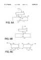
- FIG. 3Ais a side view of a package substrate with the semiconductor chip of FIG. 2 located thereon;
- FIG. 3Billustrates the semiconductor package of FIG. 3A with an epoxy provided between the semiconductor chip and the package substrate;
- FIG. 3Cillustrates the semiconductor package of FIG. 3B with an epoxy fillet located about the periphery of the semiconductor chip.
- FIG. 4is a side view of a semiconductor chip according to another embodiment of the invention.
- FIG. 5is a side view of a package substrate with the semiconductor chip of FIG. 4 located thereon;
- FIG. 6Ais a view illustrating the formation of grooves in a semiconductor wafer
- FIG. 6Bis a view of the semiconductor wafer of FIG. 6A being cut.
- FIG. 6Cis a view of the semiconductor wafer of FIG. 6B after the semiconductor wafer has been cut.
- a semiconductor chip, a semiconductor package, a method of assembling a semiconductor package, and a method of producing a semiconductor chipare described.
- numerous specific detailsare set forth in order to provide a thorough understanding of the present invention. It will be evident, however, to one skilled in the art that the present invention may be practiced without these specific details. In other instances well known semiconductor processes and methods have not been described in order to not obscure the present invention.
- FIG. 2 of the accompanying drawingsillustrates a semiconductor chip 310, according to one embodiment of the invention, that has a backside 312 having a beveled edge 314.
- the semiconductor chip 310is about 29 mils thick and the bevel is about 25% of the thickness of the semiconductor chip 310. It is to be understood, however, that the present invention is not limited by the depth or size of beveled edge.
- the semiconductor chip 310also has a frontside 316 with a plurality of C4 solder connections 318 thereon.
- the solder connections 318may be substituted by solder columns, gold solder connections, or any other connecting means that is capable of providing electrical interconnect between the chip 310 and a host device, such as a package substrate, motherboard, or the like.
- Cornered backside edgesare problematic in that stress concentrations are at their highest along the pointed edges.
- nicks, scratches, or other surface defectsoften exist on such edges because of the sawing operation used in cutting the chips.
- the beveled edge 314 of the backside 312 of the semiconductor chip 310thus firstly serves to reduce stress concentrations which develop along edges of the backside 312 of the semiconductor chip 310 and, secondly, provides the backside 312 of the semiconductor chip 310 with an edge which is finished off so as to reduce the number of small nicks, scratches or other surface defects which can propagate through the semiconductor chip 310 causing severe damage thereto.
- the cornered edges of the chipare particularly susceptible to the formation of surface defects from sawing procedures and other manufacturing processes.
- beveled edge 314is not limited to any specific geometric configuration.
- the beveled edge 314can take on any form, such as rounded or angular configurations.
- FIG. 3Aillustrates a semiconductor package 410 having a package substrate 412 supporting a semiconductor chip 310 that has a backside 312 with a beveled edge 314.
- the package substrate 412has a surface 414 having a plurality of electrical contact pads 416 thereon.
- the semiconductor chip 310is located on the package substrate 412 so that the C4 solder connections 318 on the frontside 316 of the semiconductor chip 310 electrically contact the contact pads 416.
- Mechanical and electrical connection between chip 310 and package substrate 412is achieved by passing package 410 through a reflow furnace to cause the C4 solder connection 318 to be wetted onto contact pads 416.
- FIG. 3Billustrates the semiconductor package 410 of FIG. 3A wherein an epoxy underfill 418 is applied in a space provided between the semiconductor chip 310 and the package substrate 412.
- the epoxy underfill 418is introduced on a side of the semiconductor chip 310 and flows under capillary action into the space provided between the semiconductor chip 310 and the package substrate 412.
- the epoxy 418provides protection for the C4 solder connections 318 during temperature cycles and is preferably of a substance which has a coefficient of thermal expansion which is similar to the coefficient of thermal expansion of the C4 solder connections.
- the epoxyalso acts to bond chip 310 to package substrate 412.
- the epoxycontains spherical silicon dioxide particles in order to provide the epoxy with a coefficient of thermal expansion which closely matches the coefficient of thermal expansion of the C4 solder balls.
- the solder ballstypically have a coefficient of thermal expansion of about 23 ppm/° C. and the epoxy of about 20-30 ppm/° C.
- FIG. 3Cillustrates the semiconductor package 410 of FIG. 3B after application of additional epoxy fillet 420.
- the epoxy fillet 420is applied on the package substrate 412 about a periphery of the semiconductor chip 310 so as to cover a side of the semiconductor chip 310 up to a position 422 on the beveled edge 314.
- the epoxy fillet 420may be the same as or be different from the epoxy underfill 418.
- the semiconductor package 410is then heated to about 120° C. for about 30 minutes and then to about 150° C. for about 3 hours, causing the epoxy underfill 418 and fillet 420 to cure.
- the semiconductor package 410is then allowed to cool down to room temperature.
- the semiconductor chip 310is made of silicon which has a coefficient of thermal expansion of about 3.3 ppm/° C.
- the package substrate 412could have a coefficient of thermal expansion which differs from the coefficient of thermal expansion of the semiconductor chip 310 by a relatively large amount.
- the package substrate 412may have a coefficient of thermal expansion of more than 6 ppm/° C., thus differing from the coefficient of thermal expansion of the semiconductor chip 310 by at least 2.7 ppm/° C.
- the package substrate 412may, for example, be made of a plastic or other organic material with a coefficient of thermal expansion of about 17 ppm/° C.
- the buckling or bowinginduces greater stresses along the edges of the backside 312 of the semiconductor chip 310 where stress concentrations and surface defects are the most prominent.
- the stresses induced by the coefficient of thermal expansion mismatch between the package substrate 412 and the semiconductor chip 310can cause the surface defects to propagate through the semiconductor chip 310, resulting in severe damage thereto and, eventually, in electrical failure of the semiconductor chip 310.
- the problem of stress concentrations and of surface defectsare dealt with by providing the beveled edge 314 on the backside 312 of the semiconductor chip 310.
- the stress concentrationsmay be further reduced by applying the epoxy fillet 420 so as to at least partially cover the beveled edge 314 on the backside 312 of the semiconductor chip 310.
- Tensile and sheer stresseswhich tend to delaminate the semiconductor chip 310 from the package substrate 412 are reduced by the epoxy fillet 420 acting to distribute these stresses over a larger surface area.
- a further advantage of the epoxy fillet 420is that it covers and seals minor defects that remain on the surface of the beveled edge 314, thus reducing the chances that these defects will propagate through the semiconductor chip 310.
- FIG. 4illustrates a semiconductor chip 510, according to an alternative embodiment of the invention, which is similar to the semiconductor chip 310 of FIG. 2, except that the frontside 316 also has a beveled edge 512.
- the beveled edge 512serves as a funnel to assist in the introduction of an underfill epoxy around the C4 solder connections after the chip has been attached to a package substrate, motherboard, or the like, about the semiconductor chip 510.
- the semiconductor chip 510 of FIG. 4is the same as the semiconductor chip 310 of FIG. 2 in all other respects.
- FIG. 5shows semiconductor chip 510 attached to package substrate 412.
- FIGS. 6A to 6Cillustrate a method of producing the semiconductor chip 510 of FIG. 5.
- FIG. 6Aillustrates a semiconductor wafer 710 and a first wheel 712 which is used for cutting a groove into the wafer 710.
- the wafer 710has a frontside 714 and a backside 716.
- a plurality of C4 solder connections 318are provided on the frontside 714 of the wafer 710.
- the first wheel 712has an angular tip 720 which cuts generally "V" shaped grooves.
- a first "V” shaped groove 722is first cut in the frontside 714 of the wafer 710 and a second "V” shaped groove 724 is then cut parallel to the first groove 722 on the backside 716 of the wafer 710.
- FIG. 6Billustrates the use of a second wheel 726 with a disk shaped cutting edge 728 for cutting from the second "V" shaped groove 724 to the first "V" shaped groove 722 through the wafer 710.
- the wafer 710may be cut in this way in a conventional crisscross manner to sever respective semiconductor chips.
- FIG. 6Cillustrates two semiconductor chips 510, such as in FIG. 4, which have been severed in the manner as described with reference to FIG. 6b.
- the grooves 722 and 724are wider than the disk shaped cutting edge 728 so that each semiconductor chip 510 has a frontside 316 which is left with a beveled edge 512 and a backside 312 which is also left with beveled edge 314.
Landscapes
- Engineering & Computer Science (AREA)
- Computer Hardware Design (AREA)
- Microelectronics & Electronic Packaging (AREA)
- Power Engineering (AREA)
- Physics & Mathematics (AREA)
- Condensed Matter Physics & Semiconductors (AREA)
- General Physics & Mathematics (AREA)
- Manufacturing & Machinery (AREA)
- Wire Bonding (AREA)
Abstract
Description
1. Field of the Invention
This invention relates to a semiconductor chip, a semiconductor package and to a method of assembling a semiconductor package, and to a method of producing a semiconductor chip.
2. Discussion of Related Art
The term "frontside" of a semiconductor wafer or semiconductor chip, as used herein, denotes the side of the semiconductor wafer or semiconductor chip which carries integrated circuitry, and the term "backside", as used herein, denotes a side of the semiconductor wafer or the semiconductor chip opposing the frontside.
A semiconductor package usually includes a package substrate and a semiconductor chip located on or in the package substrate. Semiconductor chips are commonly produced with C4 (controlled collapse chip connect) solder connections, on a frontside thereof, for purposes of electrically contacting the integrated circuit on the frontside of the chip to contact pads on the package substrate, electronically connecting the chip to the package substrate. An epoxy is typically introduced under capillary action into a space between the semiconductor chip and the package substrate and is subsequently cured. The epoxy acts to bond the semiconductor chip to the package substrate and to protect the C4 solder connections during the temperature cycling it will experience during the product's lifetime.
The semiconductor chip is made primarily of silicon which has a coefficient of thermal expansion (CTE) of about 3.3 ppm/° C. (parts per million per ° C.). In the past, the package substrate was generally made of a ceramic material, which has a coefficient of thermal expansion that is typically below 6 ppm/° C. During heating or cooling of the semiconductor package, the coefficients of thermal expansion of the semiconductor chip and the ceramic package substrate, respectively, were not of a magnitude which caused substantial deformation caused by stress buildup in the package.
Ceramic has a relatively high dielectric constant which causes stray capacitance to build up within the package substrate, resulting in resistance-capacitance (RC) delay. The move in recent years has therefore been away from ceramic as a package substrate material to alternative materials, such as plastics or other organic materials, which have lower dielectric constants. A problem with these alternative materials, on the other hand, is that they usually have relatively high coefficients of thermal expansion, compared to the coefficient of thermal expansion of the semiconductor chip. Plastic substrates often have coefficients of thermal expansion on the order of 17 ppm/° C. Heating or cooling of the semiconductor package thus results in substantial stress and deformation in the semiconductor chip.
As discussed above and in reference to FIG. 1, anepoxy material 102, generally a glass-filled epoxy, is provided within the space between thesemiconductor chip 104 and thepackage substrate 106 and cured. The step of curing the epoxy involves elevating the temperature of thesemiconductor package 108 to a given temperature for a specific period of time. Once the curing procedure is complete, the semiconductor package is then cooled to ambient temperature. FIG. 1 illustrates anorganic semiconductor package 108 after being cured and cooled to ambient temperature. Since the CTE of theorganic package substrate 106 is much greater than the CTE of thesemiconductor chip 104, thepackage substrate 106 tends to reduce in size during cooling at a much faster rate than thesemiconductor chip 104. This causes thesemiconductor package 108 to warp in a manner that results in an outward bowing or bending of thesemiconductor chip 104.
Bending or bowing of the semiconductor chip is problematic, in that it induces greater stresses along thebackside 109 of the semiconductor chip.Surface defects 114, such as nicks and scratches, are generally present along the backside edges of the semiconductor chip as a result of the sawing procedure used to separate the chip from a wafer. Since stress concentrations along the backside edge of the chip are particularly high, bending of the chip causes the cracks to develop rapidly into longer cracks which propagate through the semiconductor chip. Propagation of the defects can cause severe damage to the chip, and can eventually cut through active circuitry on afrontside 111 of the semiconductor chip, resulting in electrical failure of the semiconductor chip.
The difference in the CTE of thesemiconductor chip 104 andorganic package substrate 106 also producestensile stresses 110 andsheer stresses 112 that act upon theepoxy interface 102 that joins the two components. These stresses tend to delaminate the epoxy interface material from the semiconductor chip, particularly at the frontside edges of the chip where higher stress concentrations reside.
According to one aspect of the invention there is provided a semiconductor chip which has a backside with a beveled edge.
The present invention is illustrated by way of example and not limitation in the figures of the accompanying drawings, in which like references indicate similar elements and in which:
FIG. 1 is a side view of a prior art semiconductor package.
FIG. 2 is a side view of a semiconductor chip according to one embodiment of the invention.
FIG. 3A is a side view of a package substrate with the semiconductor chip of FIG. 2 located thereon;
FIG. 3B illustrates the semiconductor package of FIG. 3A with an epoxy provided between the semiconductor chip and the package substrate;
FIG. 3C illustrates the semiconductor package of FIG. 3B with an epoxy fillet located about the periphery of the semiconductor chip.
FIG. 4 is a side view of a semiconductor chip according to another embodiment of the invention.
FIG. 5 is a side view of a package substrate with the semiconductor chip of FIG. 4 located thereon;
FIG. 6A is a view illustrating the formation of grooves in a semiconductor wafer;
FIG. 6B is a view of the semiconductor wafer of FIG. 6A being cut; and
FIG. 6C is a view of the semiconductor wafer of FIG. 6B after the semiconductor wafer has been cut.
A semiconductor chip, a semiconductor package, a method of assembling a semiconductor package, and a method of producing a semiconductor chip are described. In the following description, for purposes of explanation, numerous specific details are set forth in order to provide a thorough understanding of the present invention. It will be evident, however, to one skilled in the art that the present invention may be practiced without these specific details. In other instances well known semiconductor processes and methods have not been described in order to not obscure the present invention.
FIG. 2 of the accompanying drawings illustrates asemiconductor chip 310, according to one embodiment of the invention, that has abackside 312 having abeveled edge 314. In one embodiment, thesemiconductor chip 310 is about 29 mils thick and the bevel is about 25% of the thickness of thesemiconductor chip 310. It is to be understood, however, that the present invention is not limited by the depth or size of beveled edge. Thesemiconductor chip 310 also has afrontside 316 with a plurality ofC4 solder connections 318 thereon. Thesolder connections 318 may be substituted by solder columns, gold solder connections, or any other connecting means that is capable of providing electrical interconnect between thechip 310 and a host device, such as a package substrate, motherboard, or the like.
Cornered backside edges are problematic in that stress concentrations are at their highest along the pointed edges. In addition, nicks, scratches, or other surface defects often exist on such edges because of the sawing operation used in cutting the chips. Thebeveled edge 314 of thebackside 312 of thesemiconductor chip 310 thus firstly serves to reduce stress concentrations which develop along edges of thebackside 312 of thesemiconductor chip 310 and, secondly, provides thebackside 312 of thesemiconductor chip 310 with an edge which is finished off so as to reduce the number of small nicks, scratches or other surface defects which can propagate through thesemiconductor chip 310 causing severe damage thereto. As previously discussed, the cornered edges of the chip are particularly susceptible to the formation of surface defects from sawing procedures and other manufacturing processes.
It should be noted that the shape of thebeveled edge 314 is not limited to any specific geometric configuration. Thebeveled edge 314 can take on any form, such as rounded or angular configurations.
FIG. 3A illustrates asemiconductor package 410 having apackage substrate 412 supporting asemiconductor chip 310 that has abackside 312 with abeveled edge 314. Thepackage substrate 412 has asurface 414 having a plurality ofelectrical contact pads 416 thereon. Thesemiconductor chip 310 is located on thepackage substrate 412 so that theC4 solder connections 318 on the frontside 316 of thesemiconductor chip 310 electrically contact thecontact pads 416. Mechanical and electrical connection betweenchip 310 andpackage substrate 412 is achieved by passingpackage 410 through a reflow furnace to cause theC4 solder connection 318 to be wetted ontocontact pads 416.
FIG. 3B illustrates thesemiconductor package 410 of FIG. 3A wherein anepoxy underfill 418 is applied in a space provided between thesemiconductor chip 310 and thepackage substrate 412. Theepoxy underfill 418 is introduced on a side of thesemiconductor chip 310 and flows under capillary action into the space provided between thesemiconductor chip 310 and thepackage substrate 412. The epoxy 418 provides protection for theC4 solder connections 318 during temperature cycles and is preferably of a substance which has a coefficient of thermal expansion which is similar to the coefficient of thermal expansion of the C4 solder connections. The epoxy also acts tobond chip 310 to packagesubstrate 412. In one embodiment the epoxy contains spherical silicon dioxide particles in order to provide the epoxy with a coefficient of thermal expansion which closely matches the coefficient of thermal expansion of the C4 solder balls. The solder balls typically have a coefficient of thermal expansion of about 23 ppm/° C. and the epoxy of about 20-30 ppm/° C.
FIG. 3C illustrates thesemiconductor package 410 of FIG. 3B after application of additionalepoxy fillet 420. Theepoxy fillet 420 is applied on thepackage substrate 412 about a periphery of thesemiconductor chip 310 so as to cover a side of thesemiconductor chip 310 up to aposition 422 on thebeveled edge 314. Theepoxy fillet 420 may be the same as or be different from theepoxy underfill 418.
Thesemiconductor package 410 is then heated to about 120° C. for about 30 minutes and then to about 150° C. for about 3 hours, causing theepoxy underfill 418 andfillet 420 to cure. Thesemiconductor package 410 is then allowed to cool down to room temperature.
Thesemiconductor chip 310 is made of silicon which has a coefficient of thermal expansion of about 3.3 ppm/° C. Thepackage substrate 412 could have a coefficient of thermal expansion which differs from the coefficient of thermal expansion of thesemiconductor chip 310 by a relatively large amount. For example, thepackage substrate 412 may have a coefficient of thermal expansion of more than 6 ppm/° C., thus differing from the coefficient of thermal expansion of thesemiconductor chip 310 by at least 2.7 ppm/° C. Thepackage substrate 412 may, for example, be made of a plastic or other organic material with a coefficient of thermal expansion of about 17 ppm/° C. These differences in coefficients of thermal expansion result in buckling or bowing of thesemiconductor chip 310 when thesemiconductor package 410 is being heated or cooled. The buckling or bowing induces greater stresses along the edges of thebackside 312 of thesemiconductor chip 310 where stress concentrations and surface defects are the most prominent. The stresses induced by the coefficient of thermal expansion mismatch between thepackage substrate 412 and thesemiconductor chip 310 can cause the surface defects to propagate through thesemiconductor chip 310, resulting in severe damage thereto and, eventually, in electrical failure of thesemiconductor chip 310. As hereinbefore described, the problem of stress concentrations and of surface defects are dealt with by providing thebeveled edge 314 on thebackside 312 of thesemiconductor chip 310.
The stress concentrations may be further reduced by applying theepoxy fillet 420 so as to at least partially cover thebeveled edge 314 on thebackside 312 of thesemiconductor chip 310. Tensile and sheer stresses which tend to delaminate thesemiconductor chip 310 from thepackage substrate 412 are reduced by theepoxy fillet 420 acting to distribute these stresses over a larger surface area. A further advantage of theepoxy fillet 420 is that it covers and seals minor defects that remain on the surface of thebeveled edge 314, thus reducing the chances that these defects will propagate through thesemiconductor chip 310.
It is therefore possible to use asemiconductor chip 310 on apackage substrate 412 wherein thesemiconductor chip 310 and thepackage substrate 412 have coefficients of thermal expansion which differ by a relatively large amount, without surface defects and cracks propagating from the area of the edge of thebackside 312 of thesemiconductor chip 310 during heating or cooling of thesemiconductor package 410, and without thesemiconductor chip 310 delaminating from thesubstrate package 412.
FIG. 4 illustrates asemiconductor chip 510, according to an alternative embodiment of the invention, which is similar to thesemiconductor chip 310 of FIG. 2, except that the frontside 316 also has abeveled edge 512. Thebeveled edge 512 serves as a funnel to assist in the introduction of an underfill epoxy around the C4 solder connections after the chip has been attached to a package substrate, motherboard, or the like, about thesemiconductor chip 510. Thesemiconductor chip 510 of FIG. 4 is the same as thesemiconductor chip 310 of FIG. 2 in all other respects.
FIG. 5 showssemiconductor chip 510 attached to packagesubstrate 412.
FIGS. 6A to 6C illustrate a method of producing thesemiconductor chip 510 of FIG. 5.
FIG. 6A illustrates asemiconductor wafer 710 and afirst wheel 712 which is used for cutting a groove into thewafer 710.
Thewafer 710 has a frontside 714 and abackside 716. A plurality ofC4 solder connections 318 are provided on the frontside 714 of thewafer 710.
Thefirst wheel 712 has anangular tip 720 which cuts generally "V" shaped grooves. A first "V" shapedgroove 722 is first cut in the frontside 714 of thewafer 710 and a second "V" shapedgroove 724 is then cut parallel to thefirst groove 722 on thebackside 716 of thewafer 710.
FIG. 6B illustrates the use of asecond wheel 726 with a disk shapedcutting edge 728 for cutting from the second "V" shapedgroove 724 to the first "V" shapedgroove 722 through thewafer 710. Thewafer 710 may be cut in this way in a conventional crisscross manner to sever respective semiconductor chips.
FIG. 6C illustrates twosemiconductor chips 510, such as in FIG. 4, which have been severed in the manner as described with reference to FIG. 6b. Thegrooves cutting edge 728 so that eachsemiconductor chip 510 has a frontside 316 which is left with abeveled edge 512 and abackside 312 which is also left withbeveled edge 314.
Thus, a semiconductor chip, a semiconductor package, a method of assembling a semiconductor package, and a method of producing a semiconductor chip have been described. Although the present invention has been described with reference to specific exemplary embodiments, it will be evident that various modifications and changes may be made to these embodiments without departing from the broader spirit and scope of the invention. Accordingly, the specification and drawings are to be regarded in an illustrative rather than a restrictive sense.
Claims (10)
1. A semiconductor package which includes:
a package substrate of an organic material having a coefficient of thermal expansion of at least 15 ppm/° C., the package substrate having a plurality of contact pads;
a semiconductor chip having a coefficient of thermal expansion which is at least 2.7 ppm/° C. less than the coefficient of thermal expansion of the package substrate, a backside with a beveled edge on at least two sides thereof, and a frontside with a beveled edge, the frontside having a plurality of solder connections thereon, the semiconductor chip being located on the package substrate with the solder connections contacting the contact pads and electrically coupling the semiconductor chip to the package substrate; and
an epoxy located between the semiconductor chip and the package substrate around the solder connections, the epoxy bonding the semiconductor chip to the package substrate, the epoxy further being located about a periphery of the semiconductor chip and at least partially covering the beveled edge on the frontside, and the beveled edge on the backside, the epoxy having a coefficient of thermal expansion which is similar to a coefficient of thermal expansion of the solder connections, the semiconductor package being capable of being heated to about 120° C. for about 30 minutes and then to about 150° C. for about 3 hours, and then being cooled to room temperature without defects propagating from the edge of the backside and without the semiconductor chip delaminating from the package substrate.
2. A semiconductor package which includes:
a package substrate of an organic material having a first coefficient of thermal expansion;
a semiconductor chip having a coefficient of thermal expansion which is at least 2.7 ppm/° C. less than the first coefficient of thermal expansion, the semiconductor chip having a frontside with a plurality of solder connections thereon and being located on the package substrate with the solder connections contacting the contact pads and electrically coupling the semiconductor chip to the package substrate, the semiconductor package the semiconductor package being capable of being heated to about 120° C. for about 30 minutes and then to about 150° C. for about 3 hours, and then being cooled to room temperature without defects propagating from the edge of the backside and without the semiconductor chip delaminating from the package substrate.
3. The semiconductor package of claim 2 wherein the semiconductor chip has a backside that is beveled on at least two opposing edges, and due to being beveled, is capable of being heated to about 120° C. for about 30 minutes and then to about 150° C. for about 3 hours, and then being cooled to room temperature without defects propagating from the edge of the backside and without the semiconductor chip delaminating from the package substrate.
4. The semiconductor chip of claim 2 wherein a frontside of the semiconductor chip is beveled on at least two opposing edges.
5. The semiconductor package of claim 3 which includes an epoxy located between the semiconductor chip and the package substrate around the solder connections, the epoxy bonding the semiconductor chip to the package substrate, the epoxy being further being located about a periphery of the semiconductor chip and at least partially covering the beveled edge on the backside.
6. The semiconductor package of claim 5 wherein the epoxy has a coefficient of thermal expansion which is similar to a coefficient of thermal expansion of the solder connections.
7. The semiconductor package of claim 6 wherein the frontside of the semiconductor chip is beveled on at least two opposing edges.
8. A semiconductor package which includes:
a package substrate of an organic material having a first coefficient of thermal expansion, the package substrate having a plurality of contact pads;
a semiconductor chip having a second coefficient of thermal expansion which is at least 2.7 ppm/° C. less than the first coefficient of thermal expansion, a backside which is beveled on at least two opposing edges, the semiconductor chip being located on the package substrate with the solder connections contacting the contact pads and electrically coupling the semiconductor chip to the package substrate, the semiconductor chip, due to being beveled, being capable of being heated to about 120° C. for about 30 minutes and then to about 150° C. for about 3 hours, and then being cooled to room temperature without defects propagating from the edge of the backside and without the semiconductor chip delamination from the package substrate.
9. The semiconductor chip of claim 8 which includes an epoxy located between the semiconductor chip and the package substrate around the solder connections, the epoxy bonding the semiconductor chip to the package substrate, the epoxy being further being located about a periphery of the semiconductor chip and at least partially covering the beveled edge on the backside.
10. The semiconductor chip of claim 9 wherein the epoxy has a coefficient of thermal expansion which is similar to a coefficient of thermal expansion of the solder connections.
Priority Applications (1)
| Application Number | Priority Date | Filing Date | Title |
|---|---|---|---|
| US08/988,231US6049124A (en) | 1997-12-10 | 1997-12-10 | Semiconductor package |
Applications Claiming Priority (1)
| Application Number | Priority Date | Filing Date | Title |
|---|---|---|---|
| US08/988,231US6049124A (en) | 1997-12-10 | 1997-12-10 | Semiconductor package |
Publications (1)
| Publication Number | Publication Date |
|---|---|
| US6049124Atrue US6049124A (en) | 2000-04-11 |
Family
ID=25533950
Family Applications (1)
| Application Number | Title | Priority Date | Filing Date |
|---|---|---|---|
| US08/988,231Expired - LifetimeUS6049124A (en) | 1997-12-10 | 1997-12-10 | Semiconductor package |
Country Status (1)
| Country | Link |
|---|---|
| US (1) | US6049124A (en) |
Cited By (69)
| Publication number | Priority date | Publication date | Assignee | Title |
|---|---|---|---|---|
| US6303992B1 (en)* | 1999-07-06 | 2001-10-16 | Visteon Global Technologies, Inc. | Interposer for mounting semiconductor dice on substrates |
| US6331446B1 (en) | 1999-03-03 | 2001-12-18 | Intel Corporation | Process for underfilling a controlled collapse chip connection (C4) integrated circuit package with an underfill material that is heated to a partial gel state |
| US6376915B1 (en)* | 1999-02-26 | 2002-04-23 | Rohm Co., Ltd | Semiconductor device and semiconductor chip |
| US20020089040A1 (en)* | 1998-02-27 | 2002-07-11 | Fijitsu Limited | Semiconductor device having a ball grid array and a fabrication process thereof |
| US20030001281A1 (en)* | 2001-06-29 | 2003-01-02 | Kwon Yong Hwan | Stacked chip package having upper chip provided with trenches and method of manufacturing the same |
| US6502926B2 (en) | 2001-01-30 | 2003-01-07 | Lexmark International, Inc. | Ink jet semiconductor chip structure |
| US20030006493A1 (en)* | 2001-07-04 | 2003-01-09 | Matsushita Electric Industrial Co., Ltd. | Semiconductor device and manufacturing method thereof |
| US20030025183A1 (en)* | 2001-08-01 | 2003-02-06 | Fairchild Semiconductor Corporation | Packaged semiconductor device and method of manufacture using shaped die |
| US6528345B1 (en) | 1999-03-03 | 2003-03-04 | Intel Corporation | Process line for underfilling a controlled collapse |
| US6580152B2 (en)* | 2001-08-21 | 2003-06-17 | Oki Electric Industry Co., Ltd. | Semiconductor with plural side faces |
| US20030116860A1 (en)* | 2001-12-21 | 2003-06-26 | Biju Chandran | Semiconductor package with low resistance package-to-die interconnect scheme for reduced die stresses |
| US6600213B2 (en)* | 1998-02-27 | 2003-07-29 | International Business Machines Corporation | Semiconductor structure and package including a chip having chamfered edges |
| US20030159278A1 (en)* | 2002-02-26 | 2003-08-28 | Peddle Charles I. | Methods and apparatus for fabricating Chip-on-Board modules |
| US6635963B2 (en)* | 1999-04-01 | 2003-10-21 | Oki Electric Industry Co., Ltd. | Semiconductor package with a chip connected to a wiring substrate using bump electrodes and underfilled with sealing resin |
| US6646325B2 (en) | 2001-08-21 | 2003-11-11 | Oki Electric Industry Co, Ltd. | Semiconductor device having a step-like section on the back side of the substrate, and method for manufacturing the same |
| US20040035606A1 (en)* | 2001-11-16 | 2004-02-26 | Deeney Jeffrey L. | Method and apparatus for supporting a circuit component having solder column interconnects using an external support |
| US6700178B2 (en)* | 2001-03-09 | 2004-03-02 | Advanced Semiconductor Engineering, Inc. | Package of a chip with beveled edges |
| US6731012B1 (en)* | 1999-12-23 | 2004-05-04 | International Business Machines Corporation | Non-planar surface for semiconductor chips |
| US20040104486A1 (en)* | 2000-02-16 | 2004-06-03 | Micron Technology, Inc. | Electronic apparatus having an adhesive layer from wafer level packaging |
| US6759745B2 (en)* | 2001-09-13 | 2004-07-06 | Texas Instruments Incorporated | Semiconductor device and manufacturing method thereof |
| EP1283551A3 (en)* | 2001-08-08 | 2004-07-28 | Shin-Etsu Chemical Co., Ltd. | Angular substrates |
| US6791197B1 (en)* | 2002-08-26 | 2004-09-14 | Integrated Device Technology, Inc. | Reducing layer separation and cracking in semiconductor devices |
| US6790709B2 (en) | 2001-11-30 | 2004-09-14 | Intel Corporation | Backside metallization on microelectronic dice having beveled sides for effective thermal contact with heat dissipation devices |
| US20050001219A1 (en)* | 2003-07-01 | 2005-01-06 | Matsushita Electric Industrial Co., Ltd. | Solid-state imaging device and method for manufacturing the same |
| US20050239269A1 (en)* | 2004-04-27 | 2005-10-27 | Phoenix Precision Technology Corporation | Method for releasing stress of embedded chip and chip embedded structure |
| US6995476B2 (en)* | 1998-07-01 | 2006-02-07 | Seiko Epson Corporation | Semiconductor device, circuit board and electronic instrument that include an adhesive with conductive particles therein |
| WO2006043122A1 (en)* | 2004-10-21 | 2006-04-27 | Infineon Technologies Ag | Semiconductor package and method to produce the same |
| US20060197203A1 (en)* | 2005-03-03 | 2006-09-07 | Advanced Semiconductor Engineering, Inc. | Die structure of package and method of manufacturing the same |
| US20060214294A1 (en)* | 2005-03-28 | 2006-09-28 | Fujitsu Limited | Semiconductor device and a semiconductor device manufacturing method |
| US7141448B2 (en) | 1999-03-03 | 2006-11-28 | Intel Corporation | Controlled collapse chip connection (C4) integrated circuit package which has two dissimilar underfill materials |
| US7235886B1 (en) | 2001-12-21 | 2007-06-26 | Intel Corporation | Chip-join process to reduce elongation mismatch between the adherents and semiconductor package made thereby |
| US20070228532A1 (en)* | 2006-03-28 | 2007-10-04 | Seagate Technology Llc | Edge Coating a Microelectronic Device |
| US20080061312A1 (en)* | 2006-09-12 | 2008-03-13 | Gelcore Llc | Underfill for light emitting device |
| US20090152683A1 (en)* | 2007-12-18 | 2009-06-18 | National Semiconductor Corporation | Rounded die configuration for stress minimization and enhanced thermo-mechanical reliability |
| US20090200684A1 (en)* | 2007-12-28 | 2009-08-13 | Naomi Masuda | Flip chip package with shelf and method of manufactguring there of |
| US20090242256A1 (en)* | 2008-03-31 | 2009-10-01 | Tdk Corporation | Electronic component and electronic component module |
| US20090302427A1 (en)* | 2008-06-04 | 2009-12-10 | Michael Su | Semiconductor Chip with Reinforcement Structure |
| US7679200B2 (en) | 2007-09-11 | 2010-03-16 | Globalfoundries Inc. | Semiconductor chip with crack stop |
| US20100102435A1 (en)* | 2008-10-28 | 2010-04-29 | Advanced Micro Devices, Inc. | Method and apparatus for reducing semiconductor package tensile stress |
| US20100207281A1 (en)* | 2009-02-18 | 2010-08-19 | Michael Su | Semiconductor Chip with Reinforcement Layer |
| US20100207250A1 (en)* | 2009-02-18 | 2010-08-19 | Su Michael Z | Semiconductor Chip with Protective Scribe Structure |
| US20100314718A1 (en)* | 2009-06-14 | 2010-12-16 | Terepac | Processes and structures for IC fabrication |
| US20110068435A1 (en)* | 2009-09-18 | 2011-03-24 | Russell Hudson | Semiconductor Chip with Crack Deflection Structure |
| US20110108997A1 (en)* | 2009-04-24 | 2011-05-12 | Panasonic Corporation | Mounting method and mounting structure for semiconductor package component |
| US20110175124A1 (en)* | 2010-01-15 | 2011-07-21 | Bae Jung Hyeok | Light emitting device, method of manufacturing the same, and light emitting device package |
| US20110180897A1 (en)* | 2008-06-26 | 2011-07-28 | Nxp B.V. | Packaged semiconductor product and method for manufacture thereof |
| US20110221065A1 (en)* | 2010-03-10 | 2011-09-15 | Topacio Roden R | Methods of forming semiconductor chip underfill anchors |
| WO2012044398A1 (en)* | 2010-09-27 | 2012-04-05 | Xilinx, Inc. | Corner structure for ic die |
| US20130241044A1 (en)* | 2012-03-16 | 2013-09-19 | Samsung Electronics Co., Ltd. | Semiconductor package having protective layer and method of forming the same |
| CN103489797A (en)* | 2012-06-12 | 2014-01-01 | 星科金朋有限公司 | Integrated circuit packaging system with film assist and method of manufacture thereof |
| US8912448B2 (en) | 2012-11-30 | 2014-12-16 | Industrial Technology Research Institute | Stress relief structure |
| US9281238B2 (en)* | 2014-07-11 | 2016-03-08 | United Microelectronics Corp. | Method for fabricating interlayer dielectric layer |
| US20160181127A1 (en)* | 2014-12-22 | 2016-06-23 | United Microelectronics Corporation | Method for coupling circuit element and package structure |
| US20180374718A1 (en)* | 2017-06-23 | 2018-12-27 | Applied Materials, Inc. | Method of reconstituted substrate formation for advanced packaging applications |
| US10354934B2 (en)* | 2014-06-08 | 2019-07-16 | UTAC Headquarters Pte. Ltd. | Semiconductor packages and methods of packaging semiconductor devices |
| US20200343290A1 (en)* | 2017-01-11 | 2020-10-29 | Sony Semiconductor Solutions Corporation | Imaging element, imaging device, electronic device, and method of manufacturing imaging element |
| US20210210464A1 (en)* | 2017-11-13 | 2021-07-08 | Taiwan Semiconductor Manufacturing Company, Ltd. | Package structure and method of manufacturing the same |
| US20210233852A1 (en)* | 2020-01-29 | 2021-07-29 | Taiwan Semiconductor Manufacturing Co., Ltd. | Semiconductor Package and Method |
| US20210358823A1 (en)* | 2020-05-18 | 2021-11-18 | Advanced Semiconductor Engineering, Inc. | Semiconductor package structure and method for manufacturing the same |
| US20220293567A1 (en)* | 2019-06-26 | 2022-09-15 | Invensas Bonding Technologies, Inc. | Direct bonded stack structures for increased reliability and improved yield in microelectronics |
| US20230082912A1 (en)* | 2021-09-15 | 2023-03-16 | Samsung Electronics Co., Ltd. | Semiconductor package |
| US11791282B2 (en) | 2020-07-10 | 2023-10-17 | Samsung Electronics Co., Ltd. | Semiconductor package including part of underfill on portion of a molding material surrounding sides of logic chip and memory stack on interposer and method for manufacturing the same |
| US11824032B2 (en)* | 2021-03-18 | 2023-11-21 | Taiwan Semiconductor Manufacturing Company Limited | Die corner removal for underfill crack suppression in semiconductor die packaging |
| US20240055385A1 (en)* | 2022-08-09 | 2024-02-15 | Wistron Neweb Corporation | Package structure and method for fabricating the same |
| US12046482B2 (en) | 2018-07-06 | 2024-07-23 | Adeia Semiconductor Bonding Technologies, Inc. | Microelectronic assemblies |
| US12046569B2 (en) | 2020-06-30 | 2024-07-23 | Adeia Semiconductor Bonding Technologies Inc. | Integrated device packages with integrated device die and dummy element |
| US12113056B2 (en) | 2016-05-19 | 2024-10-08 | Adeia Semiconductor Bonding Technologies Inc. | Stacked dies and methods for forming bonded structures |
| US12266640B2 (en) | 2018-07-06 | 2025-04-01 | Adeia Semiconductor Bonding Technologies Inc. | Molded direct bonded and interconnected stack |
| US12347820B2 (en) | 2018-05-15 | 2025-07-01 | Adeia Semiconductor Bonding Technologies Inc. | Stacked devices and methods of fabrication |
Citations (10)
| Publication number | Priority date | Publication date | Assignee | Title |
|---|---|---|---|---|
| US5093708A (en)* | 1990-08-20 | 1992-03-03 | Grumman Aerospace Corporation | Multilayer integrated circuit module |
| US5311059A (en)* | 1992-01-24 | 1994-05-10 | Motorola, Inc. | Backplane grounding for flip-chip integrated circuit |
| US5319242A (en)* | 1992-03-18 | 1994-06-07 | Motorola, Inc. | Semiconductor package having an exposed die surface |
| US5450283A (en)* | 1992-11-03 | 1995-09-12 | Motorola, Inc. | Thermally enhanced semiconductor device having exposed backside and method for making the same |
| US5554887A (en)* | 1993-06-01 | 1996-09-10 | Mitsubishi Denki Kabushiki Kaisha | Plastic molded semiconductor package |
| US5641996A (en)* | 1995-01-30 | 1997-06-24 | Matsushita Electric Industrial Co., Ltd. | Semiconductor unit package, semiconductor unit packaging method, and encapsulant for use in semiconductor unit packaging |
| US5706176A (en)* | 1996-07-22 | 1998-01-06 | Xerox Corporation | Butted chip array with beveled chips |
| US5751055A (en)* | 1994-02-12 | 1998-05-12 | Shin-Etsu Handotai Co., Ltd. | Semiconductor single crystalline substrate and method for production thereof |
| US5844320A (en)* | 1996-03-06 | 1998-12-01 | Matsushita Electric Industrial Co., Ltd. | Semiconductor unit with semiconductor device mounted with conductive adhesive |
| US5898224A (en)* | 1997-01-24 | 1999-04-27 | Micron Technology, Inc. | Apparatus for packaging flip chip bare die on printed circuit boards |
- 1997
- 1997-12-10USUS08/988,231patent/US6049124A/ennot_activeExpired - Lifetime
Patent Citations (10)
| Publication number | Priority date | Publication date | Assignee | Title |
|---|---|---|---|---|
| US5093708A (en)* | 1990-08-20 | 1992-03-03 | Grumman Aerospace Corporation | Multilayer integrated circuit module |
| US5311059A (en)* | 1992-01-24 | 1994-05-10 | Motorola, Inc. | Backplane grounding for flip-chip integrated circuit |
| US5319242A (en)* | 1992-03-18 | 1994-06-07 | Motorola, Inc. | Semiconductor package having an exposed die surface |
| US5450283A (en)* | 1992-11-03 | 1995-09-12 | Motorola, Inc. | Thermally enhanced semiconductor device having exposed backside and method for making the same |
| US5554887A (en)* | 1993-06-01 | 1996-09-10 | Mitsubishi Denki Kabushiki Kaisha | Plastic molded semiconductor package |
| US5751055A (en)* | 1994-02-12 | 1998-05-12 | Shin-Etsu Handotai Co., Ltd. | Semiconductor single crystalline substrate and method for production thereof |
| US5641996A (en)* | 1995-01-30 | 1997-06-24 | Matsushita Electric Industrial Co., Ltd. | Semiconductor unit package, semiconductor unit packaging method, and encapsulant for use in semiconductor unit packaging |
| US5844320A (en)* | 1996-03-06 | 1998-12-01 | Matsushita Electric Industrial Co., Ltd. | Semiconductor unit with semiconductor device mounted with conductive adhesive |
| US5706176A (en)* | 1996-07-22 | 1998-01-06 | Xerox Corporation | Butted chip array with beveled chips |
| US5898224A (en)* | 1997-01-24 | 1999-04-27 | Micron Technology, Inc. | Apparatus for packaging flip chip bare die on printed circuit boards |
Cited By (147)
| Publication number | Priority date | Publication date | Assignee | Title |
|---|---|---|---|---|
| US20060030127A1 (en)* | 1998-02-17 | 2006-02-09 | Fujitsu Limited | Method of fabricating semiconductor device |
| US6600213B2 (en)* | 1998-02-27 | 2003-07-29 | International Business Machines Corporation | Semiconductor structure and package including a chip having chamfered edges |
| US20040259346A1 (en)* | 1998-02-27 | 2004-12-23 | Fujitsu Limited | Semiconductor device having a ball grid array and a fabrication process thereof |
| US6915795B2 (en)* | 1998-02-27 | 2005-07-12 | International Business Machines Corporation | Method and system for dicing wafers, and semiconductor structures incorporating the products thereof |
| US20020089040A1 (en)* | 1998-02-27 | 2002-07-11 | Fijitsu Limited | Semiconductor device having a ball grid array and a fabrication process thereof |
| US6455920B2 (en)* | 1998-02-27 | 2002-09-24 | Fujitsu Limited | Semiconductor device having a ball grid array and a fabrication process thereof |
| US6987054B2 (en)* | 1998-02-27 | 2006-01-17 | Fujitsu Limited | Method of fabricating a semiconductor device having a groove formed in a resin layer |
| US6784542B2 (en)* | 1998-02-27 | 2004-08-31 | Fujitsu Limited | Semiconductor device having a ball grid array and a fabrication process thereof |
| US7556985B2 (en) | 1998-02-27 | 2009-07-07 | Fujitsu Microelectronics Limited | Method of fabricating semiconductor device |
| US20040012088A1 (en)* | 1998-02-27 | 2004-01-22 | Fujitsu Limited, | Semiconductor device having a ball grid array and a fabrication process thereof |
| US6657282B2 (en) | 1998-02-27 | 2003-12-02 | Fujitsu Limited | Semiconductor device having a ball grid array and a fabrication process thereof |
| US7064047B2 (en) | 1998-02-27 | 2006-06-20 | Fujitsu Limited | Semiconductor device having a ball grid array and a fabrication process thereof |
| US6995476B2 (en)* | 1998-07-01 | 2006-02-07 | Seiko Epson Corporation | Semiconductor device, circuit board and electronic instrument that include an adhesive with conductive particles therein |
| US20060099739A1 (en)* | 1998-07-01 | 2006-05-11 | Seiko Epson Corporation | Semiconductor device and method of manufacture thereof, circuit board and electronic instrument |
| US7198984B2 (en) | 1998-07-01 | 2007-04-03 | Seiko Epson Corporation | Semiconductor device and method of manufacture thereof, circuit board and electronic instrument |
| US20070132099A1 (en)* | 1998-07-01 | 2007-06-14 | Seiko Epson Corporation | Semiconductor device and method of manufacture thereof, circuit board and electronic instrument |
| US7560819B2 (en) | 1998-07-01 | 2009-07-14 | Seiko Epson Corporation | Semiconductor device and method of manufacture thereof, circuit board and electronic instrument |
| US6376915B1 (en)* | 1999-02-26 | 2002-04-23 | Rohm Co., Ltd | Semiconductor device and semiconductor chip |
| US7141448B2 (en) | 1999-03-03 | 2006-11-28 | Intel Corporation | Controlled collapse chip connection (C4) integrated circuit package which has two dissimilar underfill materials |
| US6528345B1 (en) | 1999-03-03 | 2003-03-04 | Intel Corporation | Process line for underfilling a controlled collapse |
| US6331446B1 (en) | 1999-03-03 | 2001-12-18 | Intel Corporation | Process for underfilling a controlled collapse chip connection (C4) integrated circuit package with an underfill material that is heated to a partial gel state |
| US6867069B2 (en) | 1999-04-01 | 2005-03-15 | Oki Electric Industry Co., Ltd. | Semiconductor package with a chip connected to a wiring substrate using bump electrodes and underfilled with sealing resin |
| US6635963B2 (en)* | 1999-04-01 | 2003-10-21 | Oki Electric Industry Co., Ltd. | Semiconductor package with a chip connected to a wiring substrate using bump electrodes and underfilled with sealing resin |
| US20040023438A1 (en)* | 1999-04-01 | 2004-02-05 | Yoshimi Egawa | Semiconductor package with a chip connected to a wiring substrate using bump electrodes and underfilled with sealing resin |
| US6303992B1 (en)* | 1999-07-06 | 2001-10-16 | Visteon Global Technologies, Inc. | Interposer for mounting semiconductor dice on substrates |
| US7037753B2 (en)* | 1999-12-23 | 2006-05-02 | International Business Machines Corporation | Non-planar surface for semiconductor chips |
| US20040142508A1 (en)* | 1999-12-23 | 2004-07-22 | Brodsky William L. | Non-planar surface for semiconductor chips |
| US6731012B1 (en)* | 1999-12-23 | 2004-05-04 | International Business Machines Corporation | Non-planar surface for semiconductor chips |
| US20060258052A1 (en)* | 2000-02-16 | 2006-11-16 | Micron Technology, Inc. | Wafer level pre-packaged flip chip |
| US20040104486A1 (en)* | 2000-02-16 | 2004-06-03 | Micron Technology, Inc. | Electronic apparatus having an adhesive layer from wafer level packaging |
| US7812447B2 (en) | 2000-02-16 | 2010-10-12 | Micron Technology, Inc. | Wafer level pre-packaged flip chip |
| US7943422B2 (en) | 2000-02-16 | 2011-05-17 | Micron Technology, Inc. | Wafer level pre-packaged flip chip |
| US7808112B2 (en) | 2000-02-16 | 2010-10-05 | Micron Technology, Inc. | Wafer level pre-packaged flip chip system |
| US20060255475A1 (en)* | 2000-02-16 | 2006-11-16 | Micron Technology, Inc. | Wafer level pre-packaged flip chip system |
| US20060261493A1 (en)* | 2000-02-16 | 2006-11-23 | Micron Technology, Inc. | Wafer level pre-packaged flip chip systems |
| US20060261475A1 (en)* | 2000-02-16 | 2006-11-23 | Micron Technology, Inc. | Wafer level pre-packaged flip chip |
| US7646102B2 (en) | 2000-02-16 | 2010-01-12 | Micron Technology, Inc. | Wafer level pre-packaged flip chip systems |
| US20040113246A1 (en)* | 2000-02-16 | 2004-06-17 | Micron Technology, Inc. | Method of packaging at a wafer level |
| US6502926B2 (en) | 2001-01-30 | 2003-01-07 | Lexmark International, Inc. | Ink jet semiconductor chip structure |
| US6700178B2 (en)* | 2001-03-09 | 2004-03-02 | Advanced Semiconductor Engineering, Inc. | Package of a chip with beveled edges |
| US20050051882A1 (en)* | 2001-06-29 | 2005-03-10 | Kwon Yong Hwan | Stacked chip package having upper chip provided with trenches and method of manufacturing the same |
| US7115483B2 (en)* | 2001-06-29 | 2006-10-03 | Samsung Electronics Co., Ltd. | Stacked chip package having upper chip provided with trenches and method of manufacturing the same |
| US20030001281A1 (en)* | 2001-06-29 | 2003-01-02 | Kwon Yong Hwan | Stacked chip package having upper chip provided with trenches and method of manufacturing the same |
| US6818998B2 (en)* | 2001-06-29 | 2004-11-16 | Samsung Electronics Co., Ltd. | Stacked chip package having upper chip provided with trenches and method of manufacturing the same |
| US7595222B2 (en) | 2001-07-04 | 2009-09-29 | Panasonic Corporation | Semiconductor device and manufacturing method thereof |
| US20050146005A1 (en)* | 2001-07-04 | 2005-07-07 | Matsushita Electric Industrial Co., Ltd. | Semiconductor device and manufacturing method thereof |
| US20030006493A1 (en)* | 2001-07-04 | 2003-01-09 | Matsushita Electric Industrial Co., Ltd. | Semiconductor device and manufacturing method thereof |
| US7084488B2 (en)* | 2001-08-01 | 2006-08-01 | Fairchild Semiconductor Corporation | Packaged semiconductor device and method of manufacture using shaped die |
| US20030025183A1 (en)* | 2001-08-01 | 2003-02-06 | Fairchild Semiconductor Corporation | Packaged semiconductor device and method of manufacture using shaped die |
| EP1283551A3 (en)* | 2001-08-08 | 2004-07-28 | Shin-Etsu Chemical Co., Ltd. | Angular substrates |
| US7122280B2 (en) | 2001-08-08 | 2006-10-17 | Shin-Etsu Chemical Co., Ltd. | Angular substrates |
| US6646325B2 (en) | 2001-08-21 | 2003-11-11 | Oki Electric Industry Co, Ltd. | Semiconductor device having a step-like section on the back side of the substrate, and method for manufacturing the same |
| US20030207496A1 (en)* | 2001-08-21 | 2003-11-06 | Oki Electric Industry Co., Ltd. | Semiconductor device and method for manufacturing the same |
| US6885109B2 (en) | 2001-08-21 | 2005-04-26 | Oki Electric Industry Co., Ltd. | Semiconductor device having a step-like section on the back side of the substrate, and method for manufacturing the same |
| US6580152B2 (en)* | 2001-08-21 | 2003-06-17 | Oki Electric Industry Co., Ltd. | Semiconductor with plural side faces |
| US6759745B2 (en)* | 2001-09-13 | 2004-07-06 | Texas Instruments Incorporated | Semiconductor device and manufacturing method thereof |
| US20040035606A1 (en)* | 2001-11-16 | 2004-02-26 | Deeney Jeffrey L. | Method and apparatus for supporting a circuit component having solder column interconnects using an external support |
| US7434309B2 (en)* | 2001-11-16 | 2008-10-14 | Hewlett-Packard Development Company, L.P. | Method and apparatus for supporting a circuit component having solder column interconnects using an external support |
| US6790709B2 (en) | 2001-11-30 | 2004-09-14 | Intel Corporation | Backside metallization on microelectronic dice having beveled sides for effective thermal contact with heat dissipation devices |
| US7122403B2 (en) | 2001-12-21 | 2006-10-17 | Intel Corporation | Method of interconnecting die and substrate |
| US20050116329A1 (en)* | 2001-12-21 | 2005-06-02 | Intel Corporation | Semiconductor package with low resistance package-to-die interconnect scheme for reduced die stresses |
| US20030116860A1 (en)* | 2001-12-21 | 2003-06-26 | Biju Chandran | Semiconductor package with low resistance package-to-die interconnect scheme for reduced die stresses |
| US7235886B1 (en) | 2001-12-21 | 2007-06-26 | Intel Corporation | Chip-join process to reduce elongation mismatch between the adherents and semiconductor package made thereby |
| US7238550B2 (en)* | 2002-02-26 | 2007-07-03 | Tandon Group Ltd. | Methods and apparatus for fabricating Chip-on-Board modules |
| US20030159278A1 (en)* | 2002-02-26 | 2003-08-28 | Peddle Charles I. | Methods and apparatus for fabricating Chip-on-Board modules |
| US6791197B1 (en)* | 2002-08-26 | 2004-09-14 | Integrated Device Technology, Inc. | Reducing layer separation and cracking in semiconductor devices |
| US7294907B2 (en)* | 2003-07-01 | 2007-11-13 | Matsushita Electric Industrial Co., Ltd. | Solid-state imaging device and method for manufacturing the same |
| US20050001219A1 (en)* | 2003-07-01 | 2005-01-06 | Matsushita Electric Industrial Co., Ltd. | Solid-state imaging device and method for manufacturing the same |
| US20050239269A1 (en)* | 2004-04-27 | 2005-10-27 | Phoenix Precision Technology Corporation | Method for releasing stress of embedded chip and chip embedded structure |
| US20080006900A1 (en)* | 2004-10-21 | 2008-01-10 | Infineon Technologies Ag | Semiconductor Package and Method for Producing the Same |
| US20100314721A1 (en)* | 2004-10-21 | 2010-12-16 | Infineon Technologies Ag | Semiconductor Package and Method for Producing the Same |
| US7816235B2 (en) | 2004-10-21 | 2010-10-19 | Infineon Technologies Ag | Semiconductor package and method for producing the same |
| US8003448B2 (en)* | 2004-10-21 | 2011-08-23 | Infineon Technologies, Ag | Semiconductor package and method for producing the same |
| WO2006043122A1 (en)* | 2004-10-21 | 2006-04-27 | Infineon Technologies Ag | Semiconductor package and method to produce the same |
| US20060197203A1 (en)* | 2005-03-03 | 2006-09-07 | Advanced Semiconductor Engineering, Inc. | Die structure of package and method of manufacturing the same |
| US7586185B2 (en)* | 2005-03-28 | 2009-09-08 | Fujitsu Microelectronics Limited | Semiconductor device having a functional surface |
| US20090291515A1 (en)* | 2005-03-28 | 2009-11-26 | Fujitsu Microelectronics Limited | Semiconductor device and a semiconductor device manufacturing method |
| US20060214294A1 (en)* | 2005-03-28 | 2006-09-28 | Fujitsu Limited | Semiconductor device and a semiconductor device manufacturing method |
| US7682879B2 (en)* | 2006-03-28 | 2010-03-23 | Seagate Technology Llc | Edge coating a microelectronic device |
| US20070228532A1 (en)* | 2006-03-28 | 2007-10-04 | Seagate Technology Llc | Edge Coating a Microelectronic Device |
| US7843074B2 (en)* | 2006-09-12 | 2010-11-30 | Lumination Llc | Underfill for light emitting device |
| US20080061312A1 (en)* | 2006-09-12 | 2008-03-13 | Gelcore Llc | Underfill for light emitting device |
| US7679200B2 (en) | 2007-09-11 | 2010-03-16 | Globalfoundries Inc. | Semiconductor chip with crack stop |
| US20090152683A1 (en)* | 2007-12-18 | 2009-06-18 | National Semiconductor Corporation | Rounded die configuration for stress minimization and enhanced thermo-mechanical reliability |
| US8796864B2 (en)* | 2007-12-28 | 2014-08-05 | Spansion Llc | Flip chip bonded semiconductor device with shelf |
| US20090200684A1 (en)* | 2007-12-28 | 2009-08-13 | Naomi Masuda | Flip chip package with shelf and method of manufactguring there of |
| US8486756B2 (en)* | 2007-12-28 | 2013-07-16 | Spansion Llc | Flip chip bonded semiconductor device with shelf and method of manufacturing thereof |
| US20130277834A1 (en)* | 2007-12-28 | 2013-10-24 | Spansion Llc | Flip chip package with shelf and method of manufacturing thereof |
| US20090242256A1 (en)* | 2008-03-31 | 2009-10-01 | Tdk Corporation | Electronic component and electronic component module |
| US8149584B2 (en)* | 2008-03-31 | 2012-04-03 | Tdk Corporation | Electronic component and electronic component module |
| US7737563B2 (en)* | 2008-06-04 | 2010-06-15 | Globalfoundries Inc. | Semiconductor chip with reinforcement structure |
| US20090302427A1 (en)* | 2008-06-04 | 2009-12-10 | Michael Su | Semiconductor Chip with Reinforcement Structure |
| US20110180897A1 (en)* | 2008-06-26 | 2011-07-28 | Nxp B.V. | Packaged semiconductor product and method for manufacture thereof |
| US8963314B2 (en)* | 2008-06-26 | 2015-02-24 | Nxp B.V. | Packaged semiconductor product and method for manufacture thereof |
| US20100102435A1 (en)* | 2008-10-28 | 2010-04-29 | Advanced Micro Devices, Inc. | Method and apparatus for reducing semiconductor package tensile stress |
| US8212346B2 (en)* | 2008-10-28 | 2012-07-03 | Global Foundries, Inc. | Method and apparatus for reducing semiconductor package tensile stress |
| US20100207281A1 (en)* | 2009-02-18 | 2010-08-19 | Michael Su | Semiconductor Chip with Reinforcement Layer |
| US7897433B2 (en) | 2009-02-18 | 2011-03-01 | Advanced Micro Devices, Inc. | Semiconductor chip with reinforcement layer and method of making the same |
| US20100207250A1 (en)* | 2009-02-18 | 2010-08-19 | Su Michael Z | Semiconductor Chip with Protective Scribe Structure |
| US8293581B2 (en) | 2009-02-18 | 2012-10-23 | Globalfoundries Inc. | Semiconductor chip with protective scribe structure |
| US20110108997A1 (en)* | 2009-04-24 | 2011-05-12 | Panasonic Corporation | Mounting method and mounting structure for semiconductor package component |
| US9331047B2 (en) | 2009-04-24 | 2016-05-03 | Panasonic Intellectual Property Management Co., Ltd. | Mounting method and mounting structure for semiconductor package component |
| US8513110B2 (en)* | 2009-06-14 | 2013-08-20 | Jayna Sheats | Processes and structures for beveled slope integrated circuits for interconnect fabrication |
| US20100314718A1 (en)* | 2009-06-14 | 2010-12-16 | Terepac | Processes and structures for IC fabrication |
| US8124448B2 (en) | 2009-09-18 | 2012-02-28 | Advanced Micro Devices, Inc. | Semiconductor chip with crack deflection structure |
| US20110068435A1 (en)* | 2009-09-18 | 2011-03-24 | Russell Hudson | Semiconductor Chip with Crack Deflection Structure |
| US8368107B2 (en)* | 2010-01-15 | 2013-02-05 | Lg Innotek Co., Ltd. | Light emitting device, method of manufacturing the same, and light emitting device package |
| US20110175124A1 (en)* | 2010-01-15 | 2011-07-21 | Bae Jung Hyeok | Light emitting device, method of manufacturing the same, and light emitting device package |
| US20110221065A1 (en)* | 2010-03-10 | 2011-09-15 | Topacio Roden R | Methods of forming semiconductor chip underfill anchors |
| US8389340B2 (en) | 2010-03-10 | 2013-03-05 | Ati Technologies Ulc | Methods of forming semiconductor chip underfill anchors |
| US8633599B2 (en) | 2010-03-10 | 2014-01-21 | Ati Technologies Ulc | Semiconductor chip with underfill anchors |
| US8058108B2 (en) | 2010-03-10 | 2011-11-15 | Ati Technologies Ulc | Methods of forming semiconductor chip underfill anchors |
| CN103229285A (en)* | 2010-09-27 | 2013-07-31 | 吉林克斯公司 | Corner structure for IC chip |
| WO2012044398A1 (en)* | 2010-09-27 | 2012-04-05 | Xilinx, Inc. | Corner structure for ic die |
| US8659169B2 (en) | 2010-09-27 | 2014-02-25 | Xilinx, Inc. | Corner structure for IC die |
| CN103229285B (en)* | 2010-09-27 | 2016-03-09 | 吉林克斯公司 | For the corner structure of integrated circuit (IC) chip |
| US20130241044A1 (en)* | 2012-03-16 | 2013-09-19 | Samsung Electronics Co., Ltd. | Semiconductor package having protective layer and method of forming the same |
| CN103489797A (en)* | 2012-06-12 | 2014-01-01 | 星科金朋有限公司 | Integrated circuit packaging system with film assist and method of manufacture thereof |
| US8912448B2 (en) | 2012-11-30 | 2014-12-16 | Industrial Technology Research Institute | Stress relief structure |
| US10354934B2 (en)* | 2014-06-08 | 2019-07-16 | UTAC Headquarters Pte. Ltd. | Semiconductor packages and methods of packaging semiconductor devices |
| US9564507B2 (en) | 2014-07-11 | 2017-02-07 | United Microelectronics Corp. | Interlayer dielectric layer with two tensile dielectric layers |
| US9281238B2 (en)* | 2014-07-11 | 2016-03-08 | United Microelectronics Corp. | Method for fabricating interlayer dielectric layer |
| US20160181127A1 (en)* | 2014-12-22 | 2016-06-23 | United Microelectronics Corporation | Method for coupling circuit element and package structure |
| US12266650B2 (en) | 2016-05-19 | 2025-04-01 | Adeia Semiconductor Bonding Technologies Inc. | Stacked dies and methods for forming bonded structures |
| US12113056B2 (en) | 2016-05-19 | 2024-10-08 | Adeia Semiconductor Bonding Technologies Inc. | Stacked dies and methods for forming bonded structures |
| US20200343290A1 (en)* | 2017-01-11 | 2020-10-29 | Sony Semiconductor Solutions Corporation | Imaging element, imaging device, electronic device, and method of manufacturing imaging element |
| US11605662B2 (en)* | 2017-01-11 | 2023-03-14 | Sony Semiconductor Solutions Corporation | Imaging element, imaging device, electronic device, and method of manufacturing imaging element |
| US10211072B2 (en)* | 2017-06-23 | 2019-02-19 | Applied Materials, Inc. | Method of reconstituted substrate formation for advanced packaging applications |
| US20180374718A1 (en)* | 2017-06-23 | 2018-12-27 | Applied Materials, Inc. | Method of reconstituted substrate formation for advanced packaging applications |
| US20210210464A1 (en)* | 2017-11-13 | 2021-07-08 | Taiwan Semiconductor Manufacturing Company, Ltd. | Package structure and method of manufacturing the same |
| US12347820B2 (en) | 2018-05-15 | 2025-07-01 | Adeia Semiconductor Bonding Technologies Inc. | Stacked devices and methods of fabrication |
| US12401011B2 (en) | 2018-05-15 | 2025-08-26 | Adeia Semiconductor Bonding Technologies Inc. | Stacked devices and methods of fabrication |
| US12046482B2 (en) | 2018-07-06 | 2024-07-23 | Adeia Semiconductor Bonding Technologies, Inc. | Microelectronic assemblies |
| US12341025B2 (en) | 2018-07-06 | 2025-06-24 | Adeia Semiconductor Bonding Technologies Inc. | Microelectronic assemblies |
| US12266640B2 (en) | 2018-07-06 | 2025-04-01 | Adeia Semiconductor Bonding Technologies Inc. | Molded direct bonded and interconnected stack |
| US20220293567A1 (en)* | 2019-06-26 | 2022-09-15 | Invensas Bonding Technologies, Inc. | Direct bonded stack structures for increased reliability and improved yield in microelectronics |
| US11955463B2 (en)* | 2019-06-26 | 2024-04-09 | Adeia Semiconductor Bonding Technologies Inc. | Direct bonded stack structures for increased reliability and improved yield in microelectronics |
| US12272677B2 (en) | 2019-06-26 | 2025-04-08 | Adeia Semiconductor Bonding Technologies Inc. | Direct bonded stack structures for increased reliability and improved yield in microelectronics |
| US20210233852A1 (en)* | 2020-01-29 | 2021-07-29 | Taiwan Semiconductor Manufacturing Co., Ltd. | Semiconductor Package and Method |
| US11854986B2 (en) | 2020-01-29 | 2023-12-26 | Taiwan Semiconductor Manufacturing Co., Ltd. | Chamfered die of semiconductor package and method for forming the same |
| US11682626B2 (en)* | 2020-01-29 | 2023-06-20 | Taiwan Semiconductor Manufacturing Co., Ltd. | Chamfered die of semiconductor package and method for forming the same |
| US20210358823A1 (en)* | 2020-05-18 | 2021-11-18 | Advanced Semiconductor Engineering, Inc. | Semiconductor package structure and method for manufacturing the same |
| US12046569B2 (en) | 2020-06-30 | 2024-07-23 | Adeia Semiconductor Bonding Technologies Inc. | Integrated device packages with integrated device die and dummy element |
| US11791282B2 (en) | 2020-07-10 | 2023-10-17 | Samsung Electronics Co., Ltd. | Semiconductor package including part of underfill on portion of a molding material surrounding sides of logic chip and memory stack on interposer and method for manufacturing the same |
| US11824032B2 (en)* | 2021-03-18 | 2023-11-21 | Taiwan Semiconductor Manufacturing Company Limited | Die corner removal for underfill crack suppression in semiconductor die packaging |
| US20230082912A1 (en)* | 2021-09-15 | 2023-03-16 | Samsung Electronics Co., Ltd. | Semiconductor package |
| US20240055385A1 (en)* | 2022-08-09 | 2024-02-15 | Wistron Neweb Corporation | Package structure and method for fabricating the same |
Similar Documents
| Publication | Publication Date | Title |
|---|---|---|
| US6049124A (en) | Semiconductor package | |
| US5936304A (en) | C4 package die backside coating | |
| US7148560B2 (en) | IC chip package structure and underfill process | |
| US6818550B2 (en) | Method of cutting a wafer into individual chips | |
| US7329598B2 (en) | Method of manufacturing a semiconductor device | |
| JP2921953B2 (en) | Method for manufacturing semiconductor device | |
| US7372137B2 (en) | Semiconductor device and manufacturing method thereof | |
| US20020047199A1 (en) | Semiconductor device, manufacturing method of semiconductor device, stack type semiconductor device, and manufacturing method of stack type semiconductor device | |
| US20020056927A1 (en) | Method of making semiconductor device having first and second sealing resins | |
| US20120244664A1 (en) | Reducing warpage for fan-out wafer level packaging | |
| KR20010049481A (en) | Semiconductor device and method of making the same | |
| JP6649308B2 (en) | Semiconductor device and manufacturing method thereof | |
| US10593607B2 (en) | Build-up package for integrated circuit devices, and methods of making same | |
| JP3262728B2 (en) | Semiconductor device and manufacturing method thereof | |
| US6734092B2 (en) | Semiconductor device and manufacturing method thereof | |
| US7037753B2 (en) | Non-planar surface for semiconductor chips | |
| JP2003124431A (en) | Wafer-form sheet, a chip-form electronic part, and their manufacturing method | |
| US11551973B2 (en) | Semiconductor device manufacturing method and semiconductor device | |
| US20010018233A1 (en) | Method of manufacturing semiconductor device | |
| US20050126686A1 (en) | Combination back grind tape and underfill for flip chips | |
| JP4107896B2 (en) | Semiconductor device and manufacturing method thereof | |
| JP3330890B2 (en) | Resin-sealed semiconductor device and method of manufacturing the same | |
| JP2002299547A (en) | Stacked semiconductor device and method of manufacturing the same | |
| KR100484888B1 (en) | Flip chip mounting method using a solderfill | |
| JP3415501B2 (en) | Method for manufacturing semiconductor device |
Legal Events
| Date | Code | Title | Description |
|---|---|---|---|
| AS | Assignment | Owner name:INTEL CORPORATION, CALIFORNIA Free format text:ASSIGNMENT OF ASSIGNORS INTEREST;ASSIGNORS:RAISER, GEORGE F.;TURTURRO, GREGORY;REEL/FRAME:008930/0516 Effective date:19971014 | |
| STCF | Information on status: patent grant | Free format text:PATENTED CASE | |
| FPAY | Fee payment | Year of fee payment:4 | |
| FPAY | Fee payment | Year of fee payment:8 | |
| FPAY | Fee payment | Year of fee payment:12 |