US6049055A - Method of producing a smart card - Google Patents
Method of producing a smart cardDownload PDFInfo
- Publication number
- US6049055A US6049055AUS08/952,318US95231897AUS6049055AUS 6049055 AUS6049055 AUS 6049055AUS 95231897 AUS95231897 AUS 95231897AUS 6049055 AUS6049055 AUS 6049055A
- Authority
- US
- United States
- Prior art keywords
- laser beam
- contacts
- applying
- forming
- laser
- Prior art date
- Legal status (The legal status is an assumption and is not a legal conclusion. Google has not performed a legal analysis and makes no representation as to the accuracy of the status listed.)
- Expired - Lifetime
Links
Images


Classifications
- H—ELECTRICITY
- H05—ELECTRIC TECHNIQUES NOT OTHERWISE PROVIDED FOR
- H05K—PRINTED CIRCUITS; CASINGS OR CONSTRUCTIONAL DETAILS OF ELECTRIC APPARATUS; MANUFACTURE OF ASSEMBLAGES OF ELECTRICAL COMPONENTS
- H05K1/00—Printed circuits
- H05K1/02—Details
- G—PHYSICS
- G06—COMPUTING OR CALCULATING; COUNTING
- G06K—GRAPHICAL DATA READING; PRESENTATION OF DATA; RECORD CARRIERS; HANDLING RECORD CARRIERS
- G06K1/00—Methods or arrangements for marking the record carrier in digital fashion
- G06K1/12—Methods or arrangements for marking the record carrier in digital fashion otherwise than by punching
- G06K1/126—Methods or arrangements for marking the record carrier in digital fashion otherwise than by punching by photographic or thermographic registration
- G—PHYSICS
- G06—COMPUTING OR CALCULATING; COUNTING
- G06K—GRAPHICAL DATA READING; PRESENTATION OF DATA; RECORD CARRIERS; HANDLING RECORD CARRIERS
- G06K19/00—Record carriers for use with machines and with at least a part designed to carry digital markings
- G06K19/06—Record carriers for use with machines and with at least a part designed to carry digital markings characterised by the kind of the digital marking, e.g. shape, nature, code
- G06K19/067—Record carriers with conductive marks, printed circuits or semiconductor circuit elements, e.g. credit or identity cards also with resonating or responding marks without active components
- G06K19/07—Record carriers with conductive marks, printed circuits or semiconductor circuit elements, e.g. credit or identity cards also with resonating or responding marks without active components with integrated circuit chips
- G06K19/077—Constructional details, e.g. mounting of circuits in the carrier
- G06K19/07743—External electrical contacts
- H—ELECTRICITY
- H05—ELECTRIC TECHNIQUES NOT OTHERWISE PROVIDED FOR
- H05K—PRINTED CIRCUITS; CASINGS OR CONSTRUCTIONAL DETAILS OF ELECTRIC APPARATUS; MANUFACTURE OF ASSEMBLAGES OF ELECTRICAL COMPONENTS
- H05K1/00—Printed circuits
- H05K1/02—Details
- H05K1/0266—Marks, test patterns or identification means
- H—ELECTRICITY
- H05—ELECTRIC TECHNIQUES NOT OTHERWISE PROVIDED FOR
- H05K—PRINTED CIRCUITS; CASINGS OR CONSTRUCTIONAL DETAILS OF ELECTRIC APPARATUS; MANUFACTURE OF ASSEMBLAGES OF ELECTRICAL COMPONENTS
- H05K1/00—Printed circuits
- H05K1/02—Details
- H05K1/11—Printed elements for providing electric connections to or between printed circuits
- H—ELECTRICITY
- H05—ELECTRIC TECHNIQUES NOT OTHERWISE PROVIDED FOR
- H05K—PRINTED CIRCUITS; CASINGS OR CONSTRUCTIONAL DETAILS OF ELECTRIC APPARATUS; MANUFACTURE OF ASSEMBLAGES OF ELECTRICAL COMPONENTS
- H05K2203/00—Indexing scheme relating to apparatus or processes for manufacturing printed circuits covered by H05K3/00
- H05K2203/10—Using electric, magnetic and electromagnetic fields; Using laser light
- H05K2203/107—Using laser light
- H—ELECTRICITY
- H05—ELECTRIC TECHNIQUES NOT OTHERWISE PROVIDED FOR
- H05K—PRINTED CIRCUITS; CASINGS OR CONSTRUCTIONAL DETAILS OF ELECTRIC APPARATUS; MANUFACTURE OF ASSEMBLAGES OF ELECTRICAL COMPONENTS
- H05K2203/00—Indexing scheme relating to apparatus or processes for manufacturing printed circuits covered by H05K3/00
- H05K2203/16—Inspection; Monitoring; Aligning
- H05K2203/161—Using chemical substances, e.g. colored or fluorescent, for facilitating optical or visual inspection
- H—ELECTRICITY
- H05—ELECTRIC TECHNIQUES NOT OTHERWISE PROVIDED FOR
- H05K—PRINTED CIRCUITS; CASINGS OR CONSTRUCTIONAL DETAILS OF ELECTRIC APPARATUS; MANUFACTURE OF ASSEMBLAGES OF ELECTRICAL COMPONENTS
- H05K3/00—Apparatus or processes for manufacturing printed circuits
- H05K3/22—Secondary treatment of printed circuits
- H05K3/24—Reinforcing the conductive pattern
- H05K3/244—Finish plating of conductors, especially of copper conductors, e.g. for pads or lands
Definitions
- the inventionrelates to a method for producing smart cards having contacts with visible information on the contacts.
- Smart cardscontain a chip module, which is a carrier element for a chip/IC module, having electrically conductive contacts. These contacts are conductively connected to corresponding connection points of the chip, thus enabling the smart card to communicate with appropriate appliances (smart card terminals).
- the chip moduleis fixed in a cutout in the smart card body which is open towards the front side of the card.
- Such smart cardshave already become very widespread in the form of phone cards, health insurance cards, GSM cards, bank cards and credit cards,
- a method for marking the metal contacts (applying visible information) of a smart card by laser engravingis described in EP 0 589 732.
- the gold layeris completely removed locally for the purpose of marking, the nickel layer situated therebelow, which is also partially removed as well, being visible.
- the associated damage to the gold layerimpairs the protection of the metal contact surfaces against corrosion and oxidation.
- the layer thicknessesare not illustrated true to scale.
- the copper layertypically has a thickness of approximately 70 ⁇ m, the nickel layer a thickness of approximately 1-5 ⁇ m, and the noble-metal layer located thereon a thickness of ⁇ 2 ⁇ m.
- FIG. 5--A wide pallet of possibilities for inscriptions of different colors is provided by further metal layers--compare FIG. 5--and an appropriate selection of the metals with regard to the reflective and absorptive properties of the pure metals as well as of the alloys between these metals.
- These layerscan be applied to a substrate electrically, by vapor deposition or by sputtering.
- the laser beam (LS)is applied to the contacts (20, 20A) in such a way that the laser beam (LS) is guided over the contacts (20, 20A) using the raster or vector method.
- the laser system designed for this purposeis shown in FIG. 2, and has a deflecting unit for the laser beam (LS) which can be driven electronically.
- Such systemsare already in use in so-called card personalization, where a laser is used to apply a number, for example, to the plastic body of the card.
- the laser used for this purposeis typically a neodymium YAG laser.
- the method according to the inventioncan thus be integrated in a simple way into the existing process of personalization.
- the most varied types of informationcan be represented visibly on the contacts (20, 20A).
- Carrying out the inscription of the contact surfaces according to the invention by means of such a systemcan be done very flexibly without reequipping; for example, application of a serial number, application of different logos for various batches of smart cards in production.
- the intensity of the laser beam (LS), the speed with which the latter is guided over the contacts, and the size of a laser spot (LF) on the contacts, which effect the local dwell time and the local radiative energy input,can be set in a simple way in this process in order to achieve an optimum result of inscription in each case.
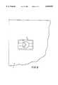
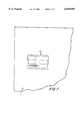
- FIG. 1shows a top view of a smart card with a chip module having contacts
- FIG. 2shows a diagrammatic view of a laser system for applying a laser beam to the contacts of the chip module of FIG. 1;
- FIG. 3is a sectional view through line III--III of the smart card of FIG. 1;
- FIG. 4is a sectional view of an embodiment of the chip module of the smart card of FIG. 1;
- FIG. 5is a sectional view of another embodiment of the chip module of the smart card of FIG. 1;
- FIGS. 6-10each show a portion of the top of the smart card of FIG. 1 with various types of visual elements applied to the contact surfaces of the chip module.
- a smart card (1) having contactsis represented in FIG. 1.
- Located in the smart card (1)is a chip module (2) fixed in a cutout which is open towards the front side of the card.
- the inventionspecifies a method for configuring the metal contacts (20A), which form the surface (20) of the chip module (2). Visible information can be produced on the contacts (20, 20A) using this method.
- laser beam (LS)is applied to the contacts (20, 20A), which comprise at least two metal layers arranged one above the other,--see FIG. 2.
- two or more layersare fused locally in each case (corresponding to the information to be represented) under the influence of the laser beam (LS) to form an alloy.
- the alloyed zonediffers in its color, that is to say in its reflection and absorption spectra, from the surrounding region of the contact.
- FIG. 3a section through the smart card (1) in the region of the chip module (2) having the contacts (20, 20A) is represented in FIG. 3. Different layered structures of the contacts (20, 20A) are represented in FIGS. 4 and 5.
- the laser beamIn order for the laser radiation not to damage the plastic substrate exposed in the insulating, metal-free interspaces between the contacts, during guidance of the laser beam (LS) over two or more contacts (20, 20A) and beyond, the laser beam is switched off, swivelled, dimmed or attenuated on its path over the insulating interspaces.
- the laser radiationis applied to the contacts (20, 20A) using the method of mask technology (not represented).
- a mask designed in accordance with information to be appliedis arranged in the beam path of the laser radiation.
- This methodis particularly advantageous in the case of large batch numbers when identical information (a mask, a mask set) is to be repeatedly applied.
- the maskis advantageously designed in such a way that it shades the laser radiation at the insulating interspaces.
- the intensity and the irradiation periodare in this case tuned to the metals to be alloyed with one another and to the number of the layers to be fused.
- the present inventionprovides, on the one hand, for inscribing smart cards already provided with contacts, both using the raster and vector methods and using the mask method. Moreover, the present invention also provides for inscribing the contacts (20, 20A) as early as on an intermediate product (not represented) for producing chip modules (2).
- the intermediate productincludes the plastic substrate and the contacts and may include the chips to be conductively connected to the contacts.
- the intermediate productmay also include a plurality of chip modules. It is the case here of so-called substrate strips to which the contacts (20, 20A) are applied to produce a multiplicity of chip modules.
- FIGS. 6 to 10show how a logo was applied by means of laser radiation on the contacts (20, 20A).
- FIG. 7shows contacts (20, 20A) with a serial number applied.
- FIG. 8shows an applied guilloche pattern,
- FIGS. 9 and 10show applied currency symbols.
Landscapes
- Engineering & Computer Science (AREA)
- Microelectronics & Electronic Packaging (AREA)
- Physics & Mathematics (AREA)
- General Physics & Mathematics (AREA)
- Theoretical Computer Science (AREA)
- Computer Hardware Design (AREA)
- Credit Cards Or The Like (AREA)
- Laser Beam Processing (AREA)
- Thermal Transfer Or Thermal Recording In General (AREA)
Abstract
Description
Claims (26)
Applications Claiming Priority (3)
| Application Number | Priority Date | Filing Date | Title |
|---|---|---|---|
| DE19606782 | 1996-02-23 | ||
| DE19606782ADE19606782C1 (en) | 1996-02-23 | 1996-02-23 | Method for producing a chip card and chip card produced therewith |
| PCT/DE1997/000318WO1997031323A1 (en) | 1996-02-23 | 1997-02-21 | Method of producing a smart card |
Publications (1)
| Publication Number | Publication Date |
|---|---|
| US6049055Atrue US6049055A (en) | 2000-04-11 |
Family
ID=7786223
Family Applications (1)
| Application Number | Title | Priority Date | Filing Date |
|---|---|---|---|
| US08/952,318Expired - LifetimeUS6049055A (en) | 1996-02-23 | 1997-02-21 | Method of producing a smart card |
Country Status (7)
| Country | Link |
|---|---|
| US (1) | US6049055A (en) |
| EP (1) | EP0823096B1 (en) |
| CN (1) | CN1180365C (en) |
| DE (2) | DE19606782C1 (en) |
| ES (1) | ES2206700T3 (en) |
| RU (1) | RU2236039C2 (en) |
| WO (1) | WO1997031323A1 (en) |
Cited By (25)
| Publication number | Priority date | Publication date | Assignee | Title |
|---|---|---|---|---|
| WO2001080160A3 (en)* | 2000-04-18 | 2002-07-04 | Laserink | Printing a code on a product |
| US20030183695A1 (en)* | 2001-12-18 | 2003-10-02 | Brian Labrec | Multiple image security features for identification documents and methods of making same |
| US6641050B2 (en) | 2001-11-06 | 2003-11-04 | International Business Machines Corporation | Secure credit card |
| US20030206227A1 (en)* | 2000-04-18 | 2003-11-06 | Laserink, A California Corporation | Printing a code on a product |
| US20050088510A1 (en)* | 2003-10-24 | 2005-04-28 | Shlomo Assa | Low angle optics and reversed optics |
| US20050134678A1 (en)* | 2003-12-19 | 2005-06-23 | Kevin Franklin | Striping and clipping correction |
| US20070119924A1 (en)* | 2001-12-31 | 2007-05-31 | Digital Data Research Company | Security Clearance Card, System And Method Of Reading A Security Clearance Card |
| EP1818851A1 (en)* | 2006-02-09 | 2007-08-15 | Axalto S.A. | Portable object having a contact interface, and personalisation of contact interface |
| US7394479B2 (en) | 2005-03-02 | 2008-07-01 | Marken Corporation | Pulsed laser printing |
| US7661600B2 (en) | 2001-12-24 | 2010-02-16 | L-1 Identify Solutions | Laser etched security features for identification documents and methods of making same |
| US7694887B2 (en) | 2001-12-24 | 2010-04-13 | L-1 Secure Credentialing, Inc. | Optically variable personalized indicia for identification documents |
| US7744002B2 (en) | 2004-03-11 | 2010-06-29 | L-1 Secure Credentialing, Inc. | Tamper evident adhesive and identification document including same |
| US7789311B2 (en) | 2003-04-16 | 2010-09-07 | L-1 Secure Credentialing, Inc. | Three dimensional data storage |
| US7793846B2 (en) | 2001-12-24 | 2010-09-14 | L-1 Secure Credentialing, Inc. | Systems, compositions, and methods for full color laser engraving of ID documents |
| US7798413B2 (en) | 2001-12-24 | 2010-09-21 | L-1 Secure Credentialing, Inc. | Covert variable information on ID documents and methods of making same |
| US7804982B2 (en) | 2002-11-26 | 2010-09-28 | L-1 Secure Credentialing, Inc. | Systems and methods for managing and detecting fraud in image databases used with identification documents |
| US7815124B2 (en) | 2002-04-09 | 2010-10-19 | L-1 Secure Credentialing, Inc. | Image processing techniques for printing identification cards and documents |
| US7824029B2 (en) | 2002-05-10 | 2010-11-02 | L-1 Secure Credentialing, Inc. | Identification card printer-assembler for over the counter card issuing |
| US7866559B2 (en) | 2004-12-28 | 2011-01-11 | L-1 Secure Credentialing, Inc. | ID document structure with pattern coating providing variable security features |
| US20110108629A1 (en)* | 2009-11-06 | 2011-05-12 | Andreas Mueller-Hipper | Smart card module with flip-chip-mounted semiconductor chip |
| US20110163167A1 (en)* | 2008-06-20 | 2011-07-07 | Smart Packaging Solutions (Sps) | Contactless card with security logo |
| US20140234572A1 (en)* | 2013-02-18 | 2014-08-21 | Nagraid S.A. | Plastic layer for a smart card |
| EP3127047A4 (en)* | 2014-04-04 | 2017-11-08 | Visa International Service Association | Payment device with holographic security element |
| US10583668B2 (en) | 2018-08-07 | 2020-03-10 | Markem-Imaje Corporation | Symbol grouping and striping for wide field matrix laser marking |
| EP3726432A1 (en)* | 2019-04-18 | 2020-10-21 | MK Smart JSC | Patterned smart card module |
Families Citing this family (8)
| Publication number | Priority date | Publication date | Assignee | Title |
|---|---|---|---|---|
| DE19606782C1 (en)* | 1996-02-23 | 1998-01-08 | Orga Kartensysteme Gmbh | Method for producing a chip card and chip card produced therewith |
| US7366690B1 (en) | 2000-06-23 | 2008-04-29 | Ebs Group Limited | Architecture for anonymous trading system |
| DE102010036057A1 (en)* | 2010-09-01 | 2012-03-01 | Giesecke & Devrient Gmbh | Chip module with marking |
| DE102012014604A1 (en)* | 2012-07-24 | 2014-05-15 | Giesecke & Devrient Gmbh | Method for producing a chip module |
| DE102015015201A1 (en)* | 2015-11-24 | 2017-05-24 | Giesecke & Devrient Gmbh | Method for individualizing a chip module together with an individualized chip module |
| DE102017003977B4 (en)* | 2017-04-25 | 2025-05-15 | e.solutions GmbH | Housing component for an electronic device, method for producing the housing component and electronic device with the housing component |
| EP3889839A1 (en)* | 2020-03-31 | 2021-10-06 | Thales Dis France Sa | Method for optimised graphic customisation of smart card modules and module obtained |
| FR3125347B1 (en) | 2021-07-16 | 2024-05-24 | Linxens Holding | Process for manufacturing multi-colored printed circuits for smart card modules |
Citations (9)
| Publication number | Priority date | Publication date | Assignee | Title |
|---|---|---|---|---|
| US4477819A (en)* | 1982-06-14 | 1984-10-16 | International Business Machines Corporation | Optical recording medium |
| US4564739A (en)* | 1983-09-15 | 1986-01-14 | Siemens Aktiengesellschaft | Apparatus for labeling parts with a laser |
| JPS61166050A (en)* | 1984-12-07 | 1986-07-26 | Fujitsu Ltd | How to stamp the IC package |
| US4849615A (en)* | 1986-04-11 | 1989-07-18 | Flonic | Apparatus for processing "smart" cards |
| EP0463930A1 (en)* | 1990-06-29 | 1992-01-02 | Thomson-Csf | Means for marking objects, method for carrying out and device for reading |
| US5198843A (en)* | 1988-06-30 | 1993-03-30 | Kabushiki Kaisha Toshiba | Optical marking system having marking mode selecting function |
| EP0653791A1 (en)* | 1993-11-12 | 1995-05-17 | Carl Baasel Lasertechnik GmbH | Device for inscribing workpieces |
| US5552574A (en)* | 1992-08-26 | 1996-09-03 | Gemplus Card International | Method for the marking of a connector of a chip card with a laser beam |
| WO1997031323A1 (en)* | 1996-02-23 | 1997-08-28 | Orga Kartensysteme Gmbh | Method of producing a smart card |
Family Cites Families (5)
| Publication number | Priority date | Publication date | Assignee | Title |
|---|---|---|---|---|
| DE3324551A1 (en)* | 1983-07-07 | 1985-01-17 | Wacker-Chemitronic Gesellschaft für Elektronik-Grundstoffe mbH, 8263 Burghausen | METHOD FOR LABELING SEMICONDUCTOR SURFACES BY LASER RADIATION |
| JPS61108195A (en)* | 1984-11-01 | 1986-05-26 | インタ−ナショナル ビジネス マシ−ンズ コ−ポレ−ション | Formation of electrically continued layers on substrate |
| DE4312095C2 (en)* | 1992-09-08 | 1996-02-01 | Borus Spezialverfahren | Process for permanent marking of an object |
| FI92112C (en)* | 1992-11-09 | 1994-09-26 | Partek Cargotec Oy | Method of designing on a glossy metal surface differs from darker from its background and a thus colored areas exhibiting metal surface |
| RU2035067C1 (en)* | 1993-05-24 | 1995-05-10 | Юрий Александрович Дьяков | Device for performing accounting operations by means of electronic card |
- 1996
- 1996-02-23DEDE19606782Apatent/DE19606782C1/ennot_activeExpired - Fee Related
- 1997
- 1997-02-21EPEP97917235Apatent/EP0823096B1/ennot_activeExpired - Lifetime
- 1997-02-21DEDE59710644Tpatent/DE59710644D1/ennot_activeExpired - Fee Related
- 1997-02-21USUS08/952,318patent/US6049055A/ennot_activeExpired - Lifetime
- 1997-02-21ESES97917235Tpatent/ES2206700T3/ennot_activeExpired - Lifetime
- 1997-02-21RURU97119057/09Apatent/RU2236039C2/ennot_activeIP Right Cessation
- 1997-02-21CNCNB97190104XApatent/CN1180365C/ennot_activeExpired - Fee Related
- 1997-02-21WOPCT/DE1997/000318patent/WO1997031323A1/enactiveIP Right Grant
Patent Citations (9)
| Publication number | Priority date | Publication date | Assignee | Title |
|---|---|---|---|---|
| US4477819A (en)* | 1982-06-14 | 1984-10-16 | International Business Machines Corporation | Optical recording medium |
| US4564739A (en)* | 1983-09-15 | 1986-01-14 | Siemens Aktiengesellschaft | Apparatus for labeling parts with a laser |
| JPS61166050A (en)* | 1984-12-07 | 1986-07-26 | Fujitsu Ltd | How to stamp the IC package |
| US4849615A (en)* | 1986-04-11 | 1989-07-18 | Flonic | Apparatus for processing "smart" cards |
| US5198843A (en)* | 1988-06-30 | 1993-03-30 | Kabushiki Kaisha Toshiba | Optical marking system having marking mode selecting function |
| EP0463930A1 (en)* | 1990-06-29 | 1992-01-02 | Thomson-Csf | Means for marking objects, method for carrying out and device for reading |
| US5552574A (en)* | 1992-08-26 | 1996-09-03 | Gemplus Card International | Method for the marking of a connector of a chip card with a laser beam |
| EP0653791A1 (en)* | 1993-11-12 | 1995-05-17 | Carl Baasel Lasertechnik GmbH | Device for inscribing workpieces |
| WO1997031323A1 (en)* | 1996-02-23 | 1997-08-28 | Orga Kartensysteme Gmbh | Method of producing a smart card |
Non-Patent Citations (1)
| Title |
|---|
| International Search Report for PCT/DE97/00318 dated Aug. 4, 1997.* |
Cited By (46)
| Publication number | Priority date | Publication date | Assignee | Title |
|---|---|---|---|---|
| WO2001080160A3 (en)* | 2000-04-18 | 2002-07-04 | Laserink | Printing a code on a product |
| US20030206227A1 (en)* | 2000-04-18 | 2003-11-06 | Laserink, A California Corporation | Printing a code on a product |
| US6791592B2 (en) | 2000-04-18 | 2004-09-14 | Laserink | Printing a code on a product |
| US6829000B2 (en) | 2000-04-18 | 2004-12-07 | Laserink | Printing a code on a product |
| EP2273420A3 (en)* | 2000-04-18 | 2015-06-10 | Laserink | Printing a code on a product |
| US7167194B2 (en) | 2000-04-18 | 2007-01-23 | Laserink | Printing a code on a product |
| US6641050B2 (en) | 2001-11-06 | 2003-11-04 | International Business Machines Corporation | Secure credit card |
| US20030183695A1 (en)* | 2001-12-18 | 2003-10-02 | Brian Labrec | Multiple image security features for identification documents and methods of making same |
| US6817530B2 (en)* | 2001-12-18 | 2004-11-16 | Digimarc Id Systems | Multiple image security features for identification documents and methods of making same |
| US7744001B2 (en) | 2001-12-18 | 2010-06-29 | L-1 Secure Credentialing, Inc. | Multiple image security features for identification documents and methods of making same |
| US8025239B2 (en) | 2001-12-18 | 2011-09-27 | L-1 Secure Credentialing, Inc. | Multiple image security features for identification documents and methods of making same |
| US8083152B2 (en) | 2001-12-24 | 2011-12-27 | L-1 Secure Credentialing, Inc. | Laser etched security features for identification documents and methods of making same |
| US7798413B2 (en) | 2001-12-24 | 2010-09-21 | L-1 Secure Credentialing, Inc. | Covert variable information on ID documents and methods of making same |
| US7793846B2 (en) | 2001-12-24 | 2010-09-14 | L-1 Secure Credentialing, Inc. | Systems, compositions, and methods for full color laser engraving of ID documents |
| US7661600B2 (en) | 2001-12-24 | 2010-02-16 | L-1 Identify Solutions | Laser etched security features for identification documents and methods of making same |
| US7694887B2 (en) | 2001-12-24 | 2010-04-13 | L-1 Secure Credentialing, Inc. | Optically variable personalized indicia for identification documents |
| US20070119924A1 (en)* | 2001-12-31 | 2007-05-31 | Digital Data Research Company | Security Clearance Card, System And Method Of Reading A Security Clearance Card |
| US7344068B2 (en)* | 2001-12-31 | 2008-03-18 | Digital Data Research Company | Security clearance card, system and method of reading a security clearance card |
| US7762456B2 (en) | 2001-12-31 | 2010-07-27 | Digital Data Research Company | Systems and methods for reading a security clearance card |
| US20100252625A1 (en)* | 2001-12-31 | 2010-10-07 | Digital Data Research Company | Systems and methods for reading a security clearance card |
| US20080156872A1 (en)* | 2001-12-31 | 2008-07-03 | Digital Data Research Company | Systems and Methods For Reading a Security Clearance Card |
| US7815124B2 (en) | 2002-04-09 | 2010-10-19 | L-1 Secure Credentialing, Inc. | Image processing techniques for printing identification cards and documents |
| US7824029B2 (en) | 2002-05-10 | 2010-11-02 | L-1 Secure Credentialing, Inc. | Identification card printer-assembler for over the counter card issuing |
| US7804982B2 (en) | 2002-11-26 | 2010-09-28 | L-1 Secure Credentialing, Inc. | Systems and methods for managing and detecting fraud in image databases used with identification documents |
| US7789311B2 (en) | 2003-04-16 | 2010-09-07 | L-1 Secure Credentialing, Inc. | Three dimensional data storage |
| US20050088510A1 (en)* | 2003-10-24 | 2005-04-28 | Shlomo Assa | Low angle optics and reversed optics |
| US7046267B2 (en) | 2003-12-19 | 2006-05-16 | Markem Corporation | Striping and clipping correction |
| US20050134678A1 (en)* | 2003-12-19 | 2005-06-23 | Kevin Franklin | Striping and clipping correction |
| US7744002B2 (en) | 2004-03-11 | 2010-06-29 | L-1 Secure Credentialing, Inc. | Tamper evident adhesive and identification document including same |
| US7963449B2 (en) | 2004-03-11 | 2011-06-21 | L-1 Secure Credentialing | Tamper evident adhesive and identification document including same |
| US7866559B2 (en) | 2004-12-28 | 2011-01-11 | L-1 Secure Credentialing, Inc. | ID document structure with pattern coating providing variable security features |
| US7394479B2 (en) | 2005-03-02 | 2008-07-01 | Marken Corporation | Pulsed laser printing |
| EP1818851A1 (en)* | 2006-02-09 | 2007-08-15 | Axalto S.A. | Portable object having a contact interface, and personalisation of contact interface |
| WO2007091158A1 (en)* | 2006-02-09 | 2007-08-16 | Axalto Sa | Portable object having a contact interface, and coloration of contact interface |
| US20110163167A1 (en)* | 2008-06-20 | 2011-07-07 | Smart Packaging Solutions (Sps) | Contactless card with security logo |
| US20110108629A1 (en)* | 2009-11-06 | 2011-05-12 | Andreas Mueller-Hipper | Smart card module with flip-chip-mounted semiconductor chip |
| US8448868B2 (en)* | 2009-11-06 | 2013-05-28 | Infineon Technologies Ag | Smart card module with flip-chip-mounted semiconductor chip |
| US20170341290A1 (en)* | 2013-02-18 | 2017-11-30 | Nagravision S.A. | Plastic layer for a smart card |
| US20140234572A1 (en)* | 2013-02-18 | 2014-08-21 | Nagraid S.A. | Plastic layer for a smart card |
| US9944011B2 (en)* | 2013-02-18 | 2018-04-17 | Nagravision S.A. | Plastic layer for a smart card |
| TWI647621B (en)* | 2013-02-18 | 2019-01-11 | 納格維遜股份有限公司 | Plastic layer for a smart card |
| EP3127047A4 (en)* | 2014-04-04 | 2017-11-08 | Visa International Service Association | Payment device with holographic security element |
| US9916580B2 (en) | 2014-04-04 | 2018-03-13 | Visa International Service Association | Payment device with holographic security element |
| US10583668B2 (en) | 2018-08-07 | 2020-03-10 | Markem-Imaje Corporation | Symbol grouping and striping for wide field matrix laser marking |
| EP3726432A1 (en)* | 2019-04-18 | 2020-10-21 | MK Smart JSC | Patterned smart card module |
| US11068767B2 (en) | 2019-04-18 | 2021-07-20 | Mk Smart Jsc | Patterned smart card module, smart card including the patterned smart card module, method for manufacturing the patterned smart card module, and method of verifying authentication of the patterned smart card module |
Also Published As
| Publication number | Publication date |
|---|---|
| ES2206700T3 (en) | 2004-05-16 |
| DE19606782C1 (en) | 1998-01-08 |
| EP0823096B1 (en) | 2003-08-27 |
| WO1997031323A1 (en) | 1997-08-28 |
| CN1180365C (en) | 2004-12-15 |
| DE59710644D1 (en) | 2003-10-02 |
| RU2236039C2 (en) | 2004-09-10 |
| CN1180433A (en) | 1998-04-29 |
| EP0823096A1 (en) | 1998-02-11 |
Similar Documents
| Publication | Publication Date | Title |
|---|---|---|
| US6049055A (en) | Method of producing a smart card | |
| RU97119057A (en) | METHOD FOR PRODUCING A CARD WITH A BUILT-IN MICROPROCESSOR AND A CARD MANUFACTURED BY THIS METHOD | |
| EP0835497B1 (en) | Chip card | |
| US5681491A (en) | Chip card having information elements etched in a metal contact of a chip card connector | |
| US4898650A (en) | Laser cleaning of metal stock | |
| JP4680999B2 (en) | Value bearing document and method for creating value bearing document | |
| DE102014106062A1 (en) | Chip card module, chip card body, chip card and smart card production method | |
| WO2007020047A2 (en) | Card-shaped data carrier | |
| CA2659902C (en) | Security elements for antennas | |
| DE19523242A1 (en) | Chip card for integrated circuit mfr. | |
| EP0733316B1 (en) | Coins and methods for producing coins | |
| CN111465721A (en) | Circuit, electronic module of a chip card implemented on said circuit and method for implementing such a circuit | |
| US11915082B2 (en) | Optimized process for graphic personalization of chip-card modules and obtained module | |
| US10223629B2 (en) | Multicolored logo on smart card modules | |
| EP2839413B1 (en) | Method of marking a chip card module by electrodeposition | |
| EP2839412B1 (en) | Method for marking a chip card module by etching | |
| US20250139397A1 (en) | RFID-Enabled Transaction Cards Of Metal And Plastic | |
| DE19604319B4 (en) | smart card | |
| WO2003038748A1 (en) | Rotary screen printing method for manufacturing an antenna |
Legal Events
| Date | Code | Title | Description |
|---|---|---|---|
| AS | Assignment | Owner name:ORGA KARTENSYSTEME GMBH, GERMANY Free format text:ASSIGNMENT OF ASSIGNORS INTEREST;ASSIGNORS:FANNASH, LOTHAR;TRUGGELMANN, UWE;REEL/FRAME:009110/0602;SIGNING DATES FROM 19971010 TO 19971012 | |
| STCF | Information on status: patent grant | Free format text:PATENTED CASE | |
| FPAY | Fee payment | Year of fee payment:4 | |
| FEPP | Fee payment procedure | Free format text:PAYOR NUMBER ASSIGNED (ORIGINAL EVENT CODE: ASPN); ENTITY STATUS OF PATENT OWNER: LARGE ENTITY | |
| FPAY | Fee payment | Year of fee payment:8 | |
| AS | Assignment | Owner name:BOEWE CARDTEC GMBH, GERMANY Free format text:ASSIGNMENT OF ASSIGNORS INTEREST;ASSIGNOR:SAGEM ORGA GMBH;REEL/FRAME:021316/0562 Effective date:20080218 Owner name:SAGEM ORGA GMBH, GERMANY Free format text:CHANGE OF NAME;ASSIGNOR:ORGA KARTENSYSTEME GMBH;REEL/FRAME:021316/0544 Effective date:20060228 | |
| AS | Assignment | Owner name:ATLANTIC ZEISER GMBH, GERMANY Free format text:ASSIGNMENT OF ASSIGNORS INTEREST;ASSIGNOR:BOEWE CARDTEC GMBH;REEL/FRAME:026784/0229 Effective date:20110323 | |
| FPAY | Fee payment | Year of fee payment:12 |